US8400082B2 - Power-saving LED lighting apparatus - Google Patents
Power-saving LED lighting apparatus Download PDFInfo
- Publication number
- US8400082B2 US8400082B2 US13/212,043 US201113212043A US8400082B2 US 8400082 B2 US8400082 B2 US 8400082B2 US 201113212043 A US201113212043 A US 201113212043A US 8400082 B2 US8400082 B2 US 8400082B2
- Authority
- US
- United States
- Prior art keywords
- led
- voltage
- lighting apparatus
- rectifier circuit
- leds
- Prior art date
- Legal status (The legal status is an assumption and is not a legal conclusion. Google has not performed a legal analysis and makes no representation as to the accuracy of the status listed.)
- Active
Links
Images


Classifications
-
- H—ELECTRICITY
- H05—ELECTRIC TECHNIQUES NOT OTHERWISE PROVIDED FOR
- H05B—ELECTRIC HEATING; ELECTRIC LIGHT SOURCES NOT OTHERWISE PROVIDED FOR; CIRCUIT ARRANGEMENTS FOR ELECTRIC LIGHT SOURCES, IN GENERAL
- H05B45/00—Circuit arrangements for operating light-emitting diodes [LED]
- H05B45/40—Details of LED load circuits
- H05B45/44—Details of LED load circuits with an active control inside an LED matrix
- H05B45/48—Details of LED load circuits with an active control inside an LED matrix having LEDs organised in strings and incorporating parallel shunting devices
Definitions
- the present invention relates to a power-saving LED lighting apparatus, and more particularly, to a power-saving LED lighting apparatus which can be driven with a full-wave rectified wave form of commercial power as a supply voltage.
- SMPS Switching Mode Power Supply
- an electric power loss of at least 15% or more occurs according to power conversion. That is, since the LED lighting apparatus having the SMPS coverts commercial power into DC voltage, and then uses the DC voltage as a driving voltage, the power efficiency is deteriorated. Further, it is necessary to establish countermeasures against noise such as EMI (Electro-Magnetic Interference) generated by switching.
- EMI Electro-Magnetic Interference
- FIG. 8 shows the principle of generating a DC voltage using a general full-wave rectifier circuit
- FIG. 9 shows wave forms of current and commercial power supplied to the full-wave rectifier circuit of FIG. 8 .
- a rectifier circuit part 610 is to full-wave rectify the commercial power, and comprised of a diode D 62 612 , a diode D 64 614 , a diode D 66 616 and a diode D 68 618 .
- a DC voltage generating part 620 is to drive a circuit of the LED lighting apparatus, and comprised of a resistor R 62 622 , a zener diode ZD 62 624 , a condenser C 62 626 and a condenser C 64 628 .
- the commercial power shown in FIG. 9 a is supplied to the rectifier circuit part 610 .
- a voltage Vcc generated from the DC voltage generating part 620 is 6V due to the rated voltage of the zener diode ZD 62 624 .
- a value of current flowing through the resistor R 62 622 and the condenser C 64 628 can be calculated from the current wave form shown in FIG. 9 b.
- an electric power consumed by the resistor R 62 622 is about 214V ⁇ 20 mA, i.e., about 4.28 W.
- An object of an embodiment of the present invention is to provide a power-saving LED lighting apparatus which can be driven with a pulsating state of full-wave rectified wave form of commercial power source as a supply voltage which is not converted into a DC voltage using a condenser.
- Another object of an embodiment of the present invention is to provide a power-saving LED lighting apparatus which can generate a DC voltage from the full-wave rectified wave form with minimum power consumption.
- an embodiment of the present invention provides a power-saving LED lighting apparatus, including a rectifier circuit part which full-wave rectifies commercial power and outputs a rectified voltage; an LED part in which a plurality of LED arrays having a plurality of LEDs are connected in series and the rectified voltage of the rectifier circuit part is supplied to an anode of the uppermost LED array; a driving part in which one terminal of each switching device for supplying or blocking a driving current to the plurality of LED arrays is connected to each anode of the plurality of LED arrays, and the other terminal thereof is connected to a cathode of the lowermost LED array; and a control part which outputs a control signal for turning on and off the switching devices of the driving part according to a level of the rectified voltage of the rectifier circuit part.
- the LED lighting apparatus further includes a constant current circuit part which is connected between the rectifier circuit part and the anode of the uppermost LED array of the LED part.
- the driving part further comprises a level shift circuit which shifts the control signal output from the control part to control the switching devices.
- the driving part may be comprised of transistors in which the switching devices are connected in parallel.
- control part has a plurality of comparators which output a control signal for turning on and off the switching devices of the driving part according to a level of the rectified voltage of the rectifier circuit part.
- each of the comparators comprises an operational amplifier having an inverting terminal and a non-inverting terminal, and a constant reference voltage is provided at the non-inverting terminal of the operational amplifier, and the rectified voltage of the rectifier circuit part is distributed to the inverting terminal.
- the voltage supplied to the non-inverting terminal of the operational amplifier is a distributed voltage obtained using resistors which are connected in series between the rectified voltage of the rectifier circuit part and the ground terminal.
- each of the LED arrays has a plurality of LEDs which are connected in the form of columns and rows of a matrix.
- a zener diode is further connected to each column of the LEDs, which are connected in the form of columns and rows of the matrix, in a reverse direction.
- an embodiment of the present invention provides a power-saving LED lighting apparatus, including an LED part in which a plurality of LED arrays having a plurality of LEDs are connected in series; a rectifier circuit part which full-wave rectifies commercial power and supplied a full-wave rectified voltage to an anode of the uppermost LED array with a ground terminal as a reference point; a DC voltage generating part which generates a DC voltage using one or more voltage-forming LEDs connected between the ground terminal and a cathode of the lowermost LED array of the LED part; a driving part which is provided with switching devices for supplying or blocking a driving current to the plurality of LED arrays; and a control part which outputs a control signal for turning on and off the switching devices of the driving part according to a level of the rectified voltage of the rectifier circuit part.
- the DC voltage generating part is further provided with a zener diode and a condenser so as to constantly maintain the DC voltage.
- the DC voltage generating part is further provided with a diode between the condenser and one or more voltage-forming LEDs in order to prevent a charged voltage of the condenser from being discharged by the one or more voltage-forming LEDs.
- each of the LED arrays has a plurality of LEDs which are connected in the form of columns and rows of a matrix, and a further voltage-forming LED is parallelly connected to the one or more voltage-forming LEDs, and the number of the parallelly connected one or more voltage-forming LEDs is smaller than the number of the parallelly connected LEDs of the LED part.
- an embodiment of the present invention does not need the high capacity condenser and transformer, it is easy to achieve the IC integration, and since there is not the high frequency generating circuit, it is not necessary for the EMI filter as a countermeasure against the noise, and thus it is possible to reduce the manufacturing cost.
- the loss of electric power is occurred only by a both-end voltage (a voltage between the emitter and the collector) of the switching devices when the switching devices are turned on, thereby minimizing the loss of electric power.
- the plurality of LEDs in the LED array are arranged in the form of a matrix, it is possible to prevent reduction in the illumination intensity which may be occurred by the disconnection of the LED or the like. And since the zener diode is applied to each column, the driving current can flow, even through all of the LEDs connected in parallel are opened.
- the level shift circuit is used in the driving part, it is possible to prevent the problem which may occur due to the voltage difference between the control part and the driving part.
- the reference voltage is supplied to the non-inverting terminal of the operational amplifier and the voltage depending on the level of rectified voltage is supplied to the inverting terminal, it is easy to detect the level according to the change in the rectified voltage.
- the present invention is provided with a separate DC power supply, or the DC power is generated from a typical AC power supply, it is possible to prevent the problem of the inherent power factor and the irrationality in the aspect of power consumption.
- FIG. 1 is a schematic view showing an operation of an LED lighting apparatus according to one embodiment of the present invention.
- FIG. 2 is a view of a wave form of a full-wave rectified voltage to explain FIG. 1 .
- FIG. 3 is a view showing a principle of generating a DC voltage in the LED lighting apparatus according to one embodiment of the present invention.
- FIG. 4 is a view showing a wave form of a full-wave rectified voltage to explain FIG. 3 .
- FIG. 5 is a view showing a detailed configuration of the LED lighting apparatus according to one embodiment of the present invention.
- FIG. 6 is a view showing a detailed configuration of an LED array used in the LED lighting apparatus of FIG. 5 .
- FIG. 7 is a view showing a detailed configuration of a constant current circuit part used in the LED lighting apparatus of FIG. 5 .
- FIG. 8 is a view showing a principle of generating a DC voltage using a general full-wave rectifier circuit.
- FIG. 9 shows wave forms of current and commercial power supplied to the full-wave rectifier circuit of FIG. 8 .
- FIG. 1 is a schematic view showing an operation of an LED lighting apparatus according to one embodiment of the present invention
- FIG. 2 is a view of a wave form of a full-wave rectified voltage to explain FIG. 1 .
- an LED lighting apparatus 100 includes an LED part 110 , a driving part 120 and a control part 130 .
- the LED part 110 includes an LED 1 112 , an LED 2 114 and an LED 3 116 which are connected in series.
- a driving voltage V 1 is supplied to an anode of the LED 3 116 , and a cathode of the LED 1 112 is connected to a ground terminal.
- the driving voltage V 1 has a wave form of full-wave rectified voltage as shown in FIG. 2 .
- the driving part 120 includes a first switching device SW 1 122 , a second switching device SW 2 124 and a third switching device SW 3 126 which supplies or blocks, in turn, a light emitting current to the LED 1 112 , the LED 2 114 and the LED 3 116 of the LED part 110 .
- the first switching device SW 1 122 is connected with the anode of the LED 1 112 and the ground terminal
- the second switching device SW 2 124 is connected with the anode of the LED 2 114 and the ground terminal
- the third switching device SW 3 126 is connected with an anode of the LED 3 116 and the ground terminal.
- the control part 130 outputs control signal which turns on or off the first switching device SW 1 122 , the second switching device SW 2 124 and the third switching device SW 3 126 , respectively.
- LED 1 112 , LED 2 114 and LED 3 116 of the LED part 110 are regarded as a single LED.
- the driving voltage V 1 supplied to the anode of the LED 3 116 has to be 10.5V or more in order to turn on all of the LED 1 112 , LED 2 114 and LED 3 116 .
- the control part 130 outputs an off signal to the first switching device SW 1 122 , the second switching device SW 2 124 and the third switching device SW 3 126 so that all of the first switching device SW 1 122 , the second switching device SW 2 124 and the third switching device SW 3 126 are switched off.
- the driving voltage V 1 supplied to the anode of the LED 3 116 is 10.5V or less, for example in a section of 7V ⁇ 10.5V in FIG. 2 , all of the LED 1 112 , LED 2 114 and LED 3 116 cannot be turned on, and thus the control part 130 outputs an on signal to the first switching device SW 1 122 so that the first switching device SW 1 122 is switched on.
- a both-end voltage of the first switching device SW 1 122 is 0V, and thus a voltage applied to the anode of the LED 1 112 is also 0V.
- the driving voltage V 1 larger than the light-emitting voltage is supplied to the LED 2 114 and the LED 3 116 , the LED 2 114 and the LED 3 116 can be continuously turned on.
- both of the LED 2 114 and the LED 3 116 cannot be turned on, and thus the control part 130 outputs an on signal to the second switching device SW 2 124 of the driving part 120 so that the second switching device SW 2 124 is switched on.
- a both-end voltage of the second switching device SW 2 124 is 0V, and thus a voltage applied to the anode of the LED 2 114 is also 0V.
- the driving voltage V 1 larger than the light-emitting voltage is supplied to the LED 3 116 , the LED 3 116 can be continuously turned on.
- the driving voltage supplied to the anode of the LED 3 116 is further lowered and thus it is 3.5V or less, for example in a section of 3.5 or less, the LED 3 116 cannot be turned on, and thus the control part 130 outputs an on signal to the third switching device SW 3 126 of the driving part 120 so that the third switching device SW 3 126 is switched on. Therefore, the driving current supplied to the LED 3 116 is blocked and all of the LED 1 112 , the LED 2 114 and the LED 3 116 are turned off.
- the control part 130 If the driving voltage supplied to the anode of the LED 3 116 is increased from 0V, the control part 130 outputs the on signal so as to switch on, in turn, the third switching device SW 3 126 , the second switching device SW 2 124 and the first switching device SW 1 122 , thereby turning on, in turn, the LED 3 116 , the LED 2 114 and the LED 1 112 .
- FIG. 3 is a view showing a principle of generating a DC voltage in the LED lighting apparatus according to one embodiment of the present invention
- FIG. 4 is a view showing a wave form of a full-wave rectified voltage to explain FIG. 3 .
- the LED lighting apparatus 100 includes a rectifier circuit part 200 , an LED part 210 , a driving part 220 and a DC voltage generating part 250 .
- the rectifier circuit part 200 is to full-wave rectify a commercial power and comprised of a diode D 12 202 , a diode D 14 204 , a diode D 16 206 and a diode D 18 208 .
- a plurality of LEDs 11 ⁇ 73 are electrically connected in the form of columns and rows of a matrix.
- the driving part 220 includes a switching device SW 1 221 for turning on or off the LED 11 , the LED 12 and the LED 13 , a switching device SW 2 222 for turning on or off the LED 21 , the LED 22 and the LED 23 , a switching device SW 6 226 for turning on or off the LED 61 , the LED 62 and the LED 63 , and a switching device SW 7 227 for turning on or off the LED 71 , the LED 72 and the LED 73 .
- the switching devices SW 1 221 , SW 2 222 , SW 6 226 and SW 7 227 are connected to each of both ends of the LEDs connected in parallel, but they may be connected in the type shown in FIG. 1 .
- the DC voltage generating part 250 is provided with a voltage-forming LED circuit 251 which is used to emit light and also to obtain a DC voltage, a zener diode ZD 1 255 for generating a desired voltage Vcc, and a condenser C 1 254 for maintaining a rated voltage of the zener diode ZD 1 255 . Further, the DC voltage generating part 250 is also provided with a resistor R 1 252 which is disposed between the voltage-forming LED circuit 251 and the zener diode ZD 1 255 so as to eliminate a difference between the both-end voltage of the voltage-forming LED circuit 251 and the rated voltage of the zener diode ZD 1 255 .
- the voltage-forming LED circuit 251 is comprised of an LED 81 , an LED 82 , an LED 91 and an LED 92 which are connected in the form of a matrix.
- the DC voltage generating part 250 may further include a diode D 1 253 between the voltage-forming LED circuit 251 and the condenser C 1 254 .
- the number (two) of voltage-forming LEDs which are connected in parallel in the DC voltage generating part 250 is smaller than the number (three) of LEDs which are connected in parallel in the LED part 210 .
- the combination of the numbers is varied according to a kind of used current.
- a proper current can flow through the voltage-forming LEDs, and at the same time, the DC voltage generating part 250 can obtain a necessary current.
- the rectifier circuit part 200 If an AC voltage is continuously supplied to the rectifier circuit part 200 , the rectifier circuit part 200 outputs a full-wave rectified voltage rectified by the diodes 202 , 204 , 206 and 208 , and the rated voltage (e.g., 6V) of the zener diode ZD 1 255 is maintained at both ends of the condenser C 1 254 by the full-wave rectified voltage.
- the rated voltage e.g., 6V
- the switching devices of the driving part 220 are switched on within a full-wave rectified voltage range of 0V ⁇ 7V and the voltage-forming LEDs (LED 81 , LED 91 and LED 92 ) of the DC voltage generating part 250 cannot be driven, the plurality of LEDs of the LED part 210 and the voltage-forming LEDs of the DC voltage generating part 250 are all turned off.
- the full-wave rectified voltage is 7V or more, the voltage-forming LEDs of the DC voltage generating part 250 , and a charging current for replenishing a discharged voltage in the condenser C 1 254 is supplied through the resistor R 1 252 and the diode D 1 253 in the meantime. Therefore, the rated voltage of the zener diode ZD 1 255 , i.e., 6V is maintained at both ends of the condenser C 1 254 .
- the switching device SW 1 221 is switched off, and the LED 11 , LED 12 and LED 13 of the LED part 210 are turned on.
- the rectified voltage is risen, more LEDs of the LED part 210 can be turned on.
- the electric power may be unnecessarily consumed by the resistor R 1 252 .
- the voltage applied to the resistor R 1 is about 1V, the consumed power is only 0.02 W (1V ⁇ 20 mA).
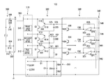
- FIG. 5 is a view showing a detailed configuration of the LED lighting apparatus according to one embodiment of the present invention.
- the LED lighting apparatus using the commercial power such as AC 220V includes a rectifier circuit part 300 , an LED part 310 , a driving part 320 , a control part 330 , a DC voltage generating part 350 and a constant current circuit part 360 .
- the rectifier circuit part 300 is to full-wave rectify the commercial power and comprised of a diode D 12 302 , a diode D 14 304 , a diode D 16 306 and a diode D 18 308 .
- the LED part 310 is comprised of a plurality of LED arrays. For convenience of explanation, it is regarded that the LED part 310 is comprised of a first LED array 312 , a second LED array 314 and a third LED array 316 .
- FIG. 6 is a view showing a detailed configuration of an LED array used in the LED lighting apparatus of FIG. 5 .
- Each of the LED arrays 312 , 314 and 316 is comprised of a plurality of LEDs, or may be comprised of white LEDs. However, as shown in FIG. 6 , it is preferable that the LED arrays 312 , 314 and 316 are comprised of the plurality of LEDs 11 ⁇ 53 which are electrically connected in the form of columns and rows of a matrix.
- LEDs 11 ⁇ 53 in a connecting method of the plurality of LEDs 11 ⁇ 53 , five LEDs, i.e., the LED 11 , LED 21 , LED 31 , LED 41 and LED 51 are electrically connected in series, and anodes of the LED 51 , LED 52 and LED 53 in a first line are electrically connected with each other, and cathodes of the LED 11 , LED 12 and LED 13 of a last line are electrically connected with each other.
- the line cannot emit the light. Therefore, in a preferable embodiment a shown in FIG. 6 , it is preferable that the nodes of the five LEDs connected in series are connected again in parallel in the form of columns and rows of a matrix. In this case, even though one of the five LEDs, e.g., the LED 32 is disconnected, other LEDs are not affected and thus the illumination intensity is not lowered remarkably.
- the zener diode is connected to every column of the LED matrix in a reverse direction. That is, the cathode of the zener diode ZD 51 is connected to the anode of the LED 51 in parallel, and the anode of the zener diode ZD 51 is connected to the cathode of the LED 51 in parallel.
- a breakdown voltage of the zener diode is slightly larger than the light-emitting voltage of the LED.
- the LED arrays 312 , 314 and 316 are arranged in a 5 ⁇ 3 matrix, but the present invention is not limited to this embodiment. Further, the number of the LED arrays 312 , 314 and 316 may be appropriately selected according to an input voltage of the commercial power.
- the driving part 320 includes a first switching circuit 322 , a second switching circuit 324 and a third switching circuit 326 which supplies or blocks, in turn, a driving current to the first, second and third LED arrays 312 , 314 and 316 of the LED part 310 .
- the first switching circuit 322 is connected with an anode terminal of the first LED array 312 and a relative ground terminal
- the second switching circuit 324 is connected with an anode terminal of the second LED array 314 and the relative ground terminal
- the third switching circuit 326 is connected with an anode terminal of the third LED array 316 and the relative ground terminal.
- the relative ground terminal is a voltage which is increased from an absolute ground point of an actual circuit due to the DC voltage generating part 350 , and indicates an area to which one ends of the first, second and third switching circuits 322 , 324 and 326 are commonly connected.
- each emitter of a first, second and third switching transistors Q 1 , Q 2 and Q 3 is connected to the cathode of the first LED array 312 .
- each collector of the switching transistors may be connected with each anode of the LED arrays 312 , 314 and 316 , and each emitter of the switching transistors may be connected with each cathode of the LED arrays 312 , 314 and 316 .
- the switching transistors which are respectively connected with the LED arrays 312 , 314 and 316 in parallel, since the switching transistors are connected in series, the unnecessary power consumption is occurred due to a sum of on-voltages applied to both ends of each switching transistor and a driving current Io, whenever the switching transistors are turned on.
- connection of the first, second and third switching transistors Q 1 , Q 2 and Q 3 shown in FIG. 5 can prevent the unnecessary power consumption which may be occurred at the connection of the switching devices of FIG. 3 . That is, in case of the first, second and third switching transistors Q 1 , Q 2 and Q 3 shown in FIG. 5 , the power consumption is occurred only by the on-voltage applied to both ends of one switching transistor and the driving current Io, and thus the unnecessary power consumption which may be occurred in FIG. 3 is prevented.
- Each switching circuit 322 , 324 , 326 is the same in FIG. 5 , and thus the first switching circuit 322 will be described as an example.
- the first switching circuit 322 is comprised of a level shift circuit including the first switching transistor Q 1 which is a semiconductor device as an example of the switching device of FIG. 1 , and a transistor TR 12 , a resistor R 12 , a resistor R 21 , a resistor 22 and a diode D 21 which turn on the first switching transistor Q 1 and shift a voltage level.
- FIG. 5 shows only the first switching transistor Q 1 as the switching device 122 of FIG. 1 , but the same switching transistor (not shown) may be further connected to be parallel with the first switching transistor Q 1 .
- a DMOS (Double Diffused MOS) transistor having low on-resistance is used as the switching transistors Q 1 , Q 2 and Q 3 .
- the control part 330 outputs control signal which switches on or off the first, second and third switching circuits 322 , 324 and 326 of the driving part 320 , respectively. That is, the control part 330 includes a first comparator 331 and a transistor TR 22 332 which control the first switching circuit 322 , a second comparator 333 and a transistor TR 24 334 which control the second switching circuit 324 , and a third comparator 335 and a transistor TR 26 336 which control the third switching circuit 326 .
- the comparators 331 , 333 and 335 have the same configuration, and the first comparator 331 is comprised of an operational amplifier OP 1 and a resistor R 31 , R 32 .
- control part 330 may include a level detecting circuit 340 .
- the level detecting circuit 340 detects a full-wave rectified voltage level, i.e., a phase value of the rectifier circuit part 300 so as to turn on or off each of the LED arrays 312 , 314 and 316 .
- the level detecting circuit 340 is comprised of the resistors R 42 , R 44 , R 46 and R 48 so as to detect the full-wave rectified voltage level. Therefore, in the level detecting circuit 340 , the voltage is distributed and applied to each node among the resistors R 42 , R 44 , R 46 and R 48 according to the rectified voltage level. The distributed voltage is supplied to the inverting terminals of the operational amplifiers.
- the DC voltage generating part 350 is connected between the absolute ground terminal and the first LED array 212 of the LED part 210 .
- the DC voltage generating part 350 is provided with an LED 81 and an LED 91 which can emit the light together with the plurality of LEDs of the LED part 210 and also can obtain the distributed voltage as the full-wave rectified voltage.
- the DC voltage generating part 350 may include the zener diode ZD 1 and the condenser C 1 so as to generate the constant voltage Vcc. Further, the DC voltage generating part 350 generates a reference voltage Vref through the resistors R 52 and R 54 and then supplies the reference voltage Vref to the non-inverting terminals of the operational amplifiers of the control part 330 .
- the constant current circuit part 360 functions to constantly maintain the current flowing through the LED arrays 312 , 314 and 316 of the LED part 360 and also to protect from an excess current.
- the constant current circuit part 360 is connected to the rectifier circuit part 300 and the anode of the third LED array 316 as the uppermost LED array of the LED part 310 .
- FIG. 7 is a view showing a detailed configuration of a constant current circuit part used in the LED lighting apparatus of FIG. 5 .
- the constant current circuit part 360 is comprised of a transistor TR 32 502 , a transistor TR 34 504 , a transistor TR 36 506 and resistors R 62 512 , R 64 514 , R 66 516 and R 68 518 .
- One end of the resistor R 62 512 is connected to collectors of the transistors TR 32 502 and TR 34 504 , and the other end thereof is connected to a base of the transistor TR 34 504 and a collector of the transistor TR 36 506 .
- one end of the resistor R 64 514 is connected to the collectors of the transistors TR 32 502 and TR 34 504 , and the other end thereof is connected to a base of the transistor TR 36 506 .
- an emitter of the transistor TR 34 504 is connected to a base of the transistor TR 32 502 .
- the resistor R 66 516 is connected between the emitter of the transistor TR 32 502 and the base of the transistor TR 36 506
- the resistor R 68 518 is connected between the emitter of the transistor TR 36 506 and the emitter of the transistor TR 32 502 .
- the transistor TR 34 504 is turned on, and thus the transistor TR 36 506 is turned on. Meanwhile, since the transistors TR 34 504 and TR 36 506 are connected in Darlington connection, an amplification degree is high.
- the full-wave rectified voltage output from the rectifier circuit part 300 is connected to the base of the transistor TR 36 506 through the resistor R 64 514 . Therefore, if the full-wave rectified voltage is increased, the voltage Vbe between the base and the emitter of the transistor TR 36 506 through the resistor R 64 506 is increased, thereby reducing the driving current Io. Accordingly, the constant current circuit part 360 can supply the constant current to the LED part 310 , even though the full-wave rectified voltage output from the rectifier circuit part 300 is increased.
- the current flowing through the resistor R 68 518 is further increased due to excess current, the voltage Vbe between the base and the emitter of the transistor TR 36 506 is also increased, and the transistor TR 34 504 is turned off, and thus the transistor TR 32 502 is turned off. Therefore, the current flowing through the LED part 310 is restricted, and thus the LED lighting apparatus 100 can be protected from the excess current.
- the commercial power e.g., 220V
- the commercial power is full-wave rectified.
- a full-wave rectified voltage of 0V is output with the ground terminal as a reference point, it is impossible to turn on the plurality of LEDs provided at the LED arrays 312 , 314 and 316 with the driving voltage supplied to each of the LED arrays 312 , 314 and 316 . Therefore, the switching transistors Q 1 , Q 2 and Q 3 of the driving part 330 should be turned on.
- each comparator 331 , 333 , 335 outputs H signal
- L signal is output to each collector of the transistors TR 22 332 , TR 24 334 and TR 36 336 .
- the transistors TR 12 , TR 14 and TR 16 of the driving part 330 are turned on by the L signal, and thus the switching transistors Q 1 , Q 2 and Q 3 are turned on.
- the full-wave rectified voltage is larger than the driving voltage, which can turn on one of the LED arrays 312 , 314 and 316 , with the ground terminal as the reference point.
- the full-wave rectified voltage is larger than the driving voltage which can turn on one of the LED arrays 312 , 314 and 316 , a distributed voltage is formed at each node point of the resistors R 42 , R 44 , R 46 and R 48 of the level detecting circuit in proportion to the resistant value and then provided at the non-inverting terminals of the operational amplifiers of the control part 330 .
- the comparator 335 since a higher voltage than the reference voltage Vref is provided at the non-inverting terminal of the operational amplifier of the comparator 335 in which the highest distributed voltage is provided, the comparator 335 outputs the L signal, and the H signal is output to the transistor TR 26 336 .
- the transistor TR 16 of the driving part 330 is turned off by the L signal, and thus the switching transistor Q 3 is also turned off. Therefore, the plurality of LEDs of the third LED array 316 of the LED part 310 is turned on.
- the full-wave rectified voltage is larger than the driving voltage, which can turn on the two of the LED arrays 312 , 314 and 316 , with the ground terminal as the reference point.
- a distributed voltage is formed at each node point of the resistors R 42 , R 44 , R 46 and R 48 of the level detecting circuit in proportion to the resistant value and then provided at the non-inverting terminals of the operational amplifiers of the control part 330 .
- the comparator 333 since a higher voltage than the reference voltage Vref is provided at the non-inverting terminal of the operational amplifier of the comparator 333 in which the second highest distributed voltage is provided, the comparator 333 outputs the L signal, and the H signal is output to the transistor TR 24 334 .
- the transistor TR 14 of the driving part 330 is turned off by the L signal, and thus the switching transistor Q 2 is also turned off. Therefore, since the plurality of LEDs of the second LED array 314 of the LED part 310 is turned on, the illumination intensity is increased more than when only the third LED array 316 is turned on.
- the full-wave rectified voltage is larger than the driving voltage, which can turn on all of the LED arrays 312 , 314 and 316 , with the ground terminal as the reference point.
- the full-wave rectified voltage is larger than the driving voltage which can turn on all of the LED arrays 312 , 314 and 316 , a distributed voltage is formed at each node point of the resistors R 42 , R 44 , R 46 and R 48 of the level detecting circuit in proportion to the resistant value and then provided at the non-inverting terminals of the operational amplifiers of the control part 330 .
- the comparator 331 outputs the L signal, and the H signal is output to the transistor TR 26 336 .
- the transistor TR 12 of the driving part 330 is turned off by the L signal, and thus the switching transistor Q 1 is also turned off. Therefore, all of the first, second and third LED arrays 312 , 314 and 316 of the LED part 310 is turned on.
- the switching transistors Q 1 , Q 2 and Q 3 are turned on in reverse order of the above-mentioned process, and thus the first, second and third LED arrays 312 , 314 and 316 are turned on in turn.
- the present invention provides the LED lighting apparatus in which the full-wave rectified wave form of the commercial power is used as the driving voltage, it is possible to improve the power factor and also to reduce the power consumption.
Landscapes
- Circuit Arrangement For Electric Light Sources In General (AREA)
- Led Devices (AREA)
- Rectifiers (AREA)
Applications Claiming Priority (5)
| Application Number | Priority Date | Filing Date | Title |
|---|---|---|---|
| KR10-2009-0013056 | 2009-02-17 | ||
| KR1020090013056A KR100971757B1 (ko) | 2009-02-17 | 2009-02-17 | Led 조명장치 |
| KR1020090028436A KR100971759B1 (ko) | 2009-04-02 | 2009-04-02 | 절전형 led 조명장치 |
| KR10-2009-0028436 | 2009-04-02 | ||
| PCT/KR2010/000114 WO2010095813A2 (ko) | 2009-02-17 | 2010-01-08 | 절전형 led 조명장치 |
Related Parent Applications (1)
| Application Number | Title | Priority Date | Filing Date |
|---|---|---|---|
| PCT/KR2010/000114 Continuation WO2010095813A2 (ko) | 2009-02-17 | 2010-01-08 | 절전형 led 조명장치 |
Publications (2)
| Publication Number | Publication Date |
|---|---|
| US20110316432A1 US20110316432A1 (en) | 2011-12-29 |
| US8400082B2 true US8400082B2 (en) | 2013-03-19 |
Family
ID=42634293
Family Applications (1)
| Application Number | Title | Priority Date | Filing Date |
|---|---|---|---|
| US13/212,043 Active US8400082B2 (en) | 2009-02-17 | 2011-08-17 | Power-saving LED lighting apparatus |
Country Status (6)
| Country | Link |
|---|---|
| US (1) | US8400082B2 (ja) |
| EP (1) | EP2400819A4 (ja) |
| JP (2) | JP2012518264A (ja) |
| CN (1) | CN102349354A (ja) |
| BR (1) | BRPI1005916A2 (ja) |
| WO (1) | WO2010095813A2 (ja) |
Cited By (4)
| Publication number | Priority date | Publication date | Assignee | Title |
|---|---|---|---|---|
| US20130257298A1 (en) * | 2012-03-29 | 2013-10-03 | Jeong In Cheon | Power compensation device and light emitting diode illumination apparatus having the same |
| US9370063B2 (en) | 2014-06-24 | 2016-06-14 | Samsung Electronics Co., Ltd. | LED driving device and lighting device |
| US9781790B2 (en) | 2010-08-12 | 2017-10-03 | Fairchild Korea Semiconductor Ltd. | Phase shift circuit and dimming circuit including the same |
| US10111286B1 (en) * | 2014-02-27 | 2018-10-23 | Inter-Global, Inc. | Driver circuit for LED light |
Families Citing this family (18)
| Publication number | Priority date | Publication date | Assignee | Title |
|---|---|---|---|---|
| EP2609794A2 (en) * | 2010-08-27 | 2013-07-03 | American Bright Lighting, Inc. | Solid state lighting driver with thdi bypass circuit |
| CN102480825A (zh) * | 2010-11-30 | 2012-05-30 | 亚德光机股份有限公司 | 发光二极管的驱动方法及其装置 |
| JP5820062B2 (ja) | 2011-05-26 | 2015-11-24 | コリア エレクトロテクノロジー リサーチ インスティチュート | Led駆動制御装置及びその駆動電流制御方法 |
| GB2496017B (en) * | 2011-10-27 | 2016-06-08 | Diehl Aerospace Gmbh | Lighting device for an AC power supply |
| GB201201689D0 (en) * | 2012-01-30 | 2012-03-14 | Trundle Robert M | Ultra clean off line led driver |
| CN104244492B (zh) * | 2012-04-07 | 2016-11-23 | 吴槐 | Led工作模式控制装置 |
| DE102012207456B4 (de) | 2012-05-04 | 2013-11-28 | Osram Gmbh | Ansteuerung von Halbleiterleuchtelementen |
| CN103716935B (zh) * | 2012-09-29 | 2016-01-13 | 钰瀚科技股份有限公司 | 基于发光二极管的多数个照明单位的驱动装置 |
| US9131567B2 (en) | 2012-10-22 | 2015-09-08 | Marvell World Trade Ltd. | Temperature foldback circuit for LED load control by constant current source |
| TWI477194B (zh) * | 2013-05-29 | 2015-03-11 | Richtek Technology Corp | Light emitting diode drive device |
| CN103596328B (zh) * | 2013-10-23 | 2015-11-25 | 浙江大学 | 一种led驱动电路 |
| WO2015141685A1 (ja) * | 2014-03-17 | 2015-09-24 | シチズンホールディングス株式会社 | Led照明装置 |
| JP6725173B2 (ja) * | 2016-08-12 | 2020-07-15 | アズビル株式会社 | インタフェース回路 |
| CN110621104A (zh) * | 2019-05-27 | 2019-12-27 | 广东明丰电源电器实业有限公司 | 一种降低待机功耗的电路及电子设备 |
| CN112135388B (zh) * | 2020-09-10 | 2022-06-10 | 无锡商业职业技术学院 | 一种led投光灯的驱动电路及其控制方法 |
| KR102316206B1 (ko) * | 2021-02-04 | 2021-10-25 | (주)알에프세미 | 다단 전류제어 발광다이오드 조명장치 |
| KR102429145B1 (ko) * | 2021-10-08 | 2022-08-05 | (주)알에프세미 | 플리커 감소 기능을 갖는 교류전원 발광다이오드 구동장치 |
| JP2023092798A (ja) * | 2021-12-22 | 2023-07-04 | 株式会社小糸製作所 | 点灯回路 |
Citations (11)
| Publication number | Priority date | Publication date | Assignee | Title |
|---|---|---|---|---|
| KR20010093337A (ko) | 1999-12-14 | 2001-10-27 | 오자키 고에이 | 전원장치 및 led 램프장치 |
| KR100453133B1 (ko) | 2001-12-14 | 2004-10-15 | 산요덴키가부시키가이샤 | 구동 회로 |
| JP2005142137A (ja) | 2003-10-15 | 2005-06-02 | Matsushita Electric Works Ltd | Led点灯装置 |
| KR200405272Y1 (ko) | 2005-10-28 | 2006-01-10 | 코디스 주식회사 | 엘이디 조명장치 |
| US20060232219A1 (en) * | 2003-05-07 | 2006-10-19 | Koninklijke Philips Electronics N.V. | Single driver for multiple light emitting diodes |
| US7265952B2 (en) * | 2005-06-09 | 2007-09-04 | Addtek Corp. | Two-terminal protecting circuit |
| US20070257623A1 (en) * | 2006-03-27 | 2007-11-08 | Texas Instruments, Incorporated | Highly efficient series string led driver with individual led control |
| JP2008059811A (ja) | 2006-08-29 | 2008-03-13 | Avago Technologies Ecbu Ip (Singapore) Pte Ltd | Ledを駆動するための装置及び方法 |
| US7521879B2 (en) * | 2005-12-22 | 2009-04-21 | Lg Display Co., Ltd. | Device for driving light emitting diode |
| US7638954B2 (en) * | 2006-01-20 | 2009-12-29 | Panasonic Corporation | Light emitting diode drive apparatus |
| US7741788B2 (en) * | 2007-02-22 | 2010-06-22 | Koito Manufacturing Co., Ltd. | Light emitting apparatus with current limiting |
Family Cites Families (6)
| Publication number | Priority date | Publication date | Assignee | Title |
|---|---|---|---|---|
| JP2004356000A (ja) * | 2003-05-30 | 2004-12-16 | Seiwa Electric Mfg Co Ltd | Led駆動回路 |
| JP4581646B2 (ja) * | 2004-11-22 | 2010-11-17 | パナソニック電工株式会社 | 発光ダイオード点灯装置 |
| JP4588494B2 (ja) * | 2005-03-03 | 2010-12-01 | 株式会社ジャムコ | 照明用発光ダイオード駆動回路 |
| JP5099661B2 (ja) * | 2005-10-28 | 2012-12-19 | 株式会社寺田電機製作所 | Led駆動回路およびled駆動方法 |
| JP5667361B2 (ja) * | 2006-09-20 | 2015-02-12 | コーニンクレッカ フィリップス エヌ ヴェ | 発光素子制御システム及び該システムを有する照明システム |
| WO2008129504A1 (en) * | 2007-04-24 | 2008-10-30 | Philips Intellectual Property & Standards Gmbh | Led string driver with shift register and level shifter |
-
2010
- 2010-01-08 BR BRPI1005916A patent/BRPI1005916A2/pt not_active IP Right Cessation
- 2010-01-08 CN CN2010800113279A patent/CN102349354A/zh active Pending
- 2010-01-08 JP JP2011550998A patent/JP2012518264A/ja active Pending
- 2010-01-08 EP EP10743888A patent/EP2400819A4/en not_active Withdrawn
- 2010-01-08 WO PCT/KR2010/000114 patent/WO2010095813A2/ko active Application Filing
-
2011
- 2011-08-17 US US13/212,043 patent/US8400082B2/en active Active
-
2013
- 2013-07-19 JP JP2013150431A patent/JP2013243147A/ja active Pending
Patent Citations (12)
| Publication number | Priority date | Publication date | Assignee | Title |
|---|---|---|---|---|
| KR20010093337A (ko) | 1999-12-14 | 2001-10-27 | 오자키 고에이 | 전원장치 및 led 램프장치 |
| KR100453133B1 (ko) | 2001-12-14 | 2004-10-15 | 산요덴키가부시키가이샤 | 구동 회로 |
| US20060232219A1 (en) * | 2003-05-07 | 2006-10-19 | Koninklijke Philips Electronics N.V. | Single driver for multiple light emitting diodes |
| JP2005142137A (ja) | 2003-10-15 | 2005-06-02 | Matsushita Electric Works Ltd | Led点灯装置 |
| US7265952B2 (en) * | 2005-06-09 | 2007-09-04 | Addtek Corp. | Two-terminal protecting circuit |
| KR200405272Y1 (ko) | 2005-10-28 | 2006-01-10 | 코디스 주식회사 | 엘이디 조명장치 |
| US7521879B2 (en) * | 2005-12-22 | 2009-04-21 | Lg Display Co., Ltd. | Device for driving light emitting diode |
| US7638954B2 (en) * | 2006-01-20 | 2009-12-29 | Panasonic Corporation | Light emitting diode drive apparatus |
| US20070257623A1 (en) * | 2006-03-27 | 2007-11-08 | Texas Instruments, Incorporated | Highly efficient series string led driver with individual led control |
| JP2008059811A (ja) | 2006-08-29 | 2008-03-13 | Avago Technologies Ecbu Ip (Singapore) Pte Ltd | Ledを駆動するための装置及び方法 |
| US7564198B2 (en) * | 2006-08-29 | 2009-07-21 | Avago Technologies Ecbu Ip (Singapore) Pte. Ltd. | Device and method for driving LED |
| US7741788B2 (en) * | 2007-02-22 | 2010-06-22 | Koito Manufacturing Co., Ltd. | Light emitting apparatus with current limiting |
Cited By (5)
| Publication number | Priority date | Publication date | Assignee | Title |
|---|---|---|---|---|
| US9781790B2 (en) | 2010-08-12 | 2017-10-03 | Fairchild Korea Semiconductor Ltd. | Phase shift circuit and dimming circuit including the same |
| US20130257298A1 (en) * | 2012-03-29 | 2013-10-03 | Jeong In Cheon | Power compensation device and light emitting diode illumination apparatus having the same |
| US8928247B2 (en) * | 2012-03-29 | 2015-01-06 | Lg Electronics Inc. | Power compensation device and light emitting diode illumination apparatus having the same |
| US10111286B1 (en) * | 2014-02-27 | 2018-10-23 | Inter-Global, Inc. | Driver circuit for LED light |
| US9370063B2 (en) | 2014-06-24 | 2016-06-14 | Samsung Electronics Co., Ltd. | LED driving device and lighting device |
Also Published As
| Publication number | Publication date |
|---|---|
| EP2400819A4 (en) | 2012-12-05 |
| CN102349354A (zh) | 2012-02-08 |
| WO2010095813A2 (ko) | 2010-08-26 |
| WO2010095813A3 (ko) | 2010-10-14 |
| BRPI1005916A2 (pt) | 2019-09-24 |
| US20110316432A1 (en) | 2011-12-29 |
| JP2012518264A (ja) | 2012-08-09 |
| EP2400819A2 (en) | 2011-12-28 |
| JP2013243147A (ja) | 2013-12-05 |
Similar Documents
| Publication | Publication Date | Title |
|---|---|---|
| US8400082B2 (en) | Power-saving LED lighting apparatus | |
| US9301353B2 (en) | Light emitting diode driving apparatus | |
| JP5720392B2 (ja) | 発光ダイオード駆動装置 | |
| JP5559264B2 (ja) | 高効率acled駆動回路 | |
| US8994289B2 (en) | LED drive circuit | |
| TWI428057B (zh) | 具有動態性負載與提升功率因素之發光驅動電路與相關的動態負載模組 | |
| US8395915B2 (en) | DC/DC converter | |
| KR101771718B1 (ko) | 발광 다이오드의 전류 구동 회로 및 이를 이용한 발광 장치, 전자 기기, 발광 다이오드의 구동 모드의 설정 방법 | |
| JP2007189004A (ja) | 直流電源装置、発光ダイオード用電源、及び照明装置 | |
| US8669709B2 (en) | Solid state lighting driver with THDi bypass circuit | |
| JP2013504175A (ja) | 定電流駆動ledモジュール装置 | |
| KR20110136537A (ko) | 과전압 보호와 정전류 구동을 위한 led 구동 회로 및 방법 | |
| US10542594B2 (en) | Direct AC driving circuit and luminaire | |
| JP2013135513A (ja) | 電力変換装置 | |
| JP2008052994A (ja) | 照明装置および制御回路 | |
| KR100971759B1 (ko) | 절전형 led 조명장치 | |
| US20140035477A1 (en) | Single stage forward-flyback converter and power supply apparatus | |
| US8981658B2 (en) | Apparatus for driving light emitting diode | |
| US9967929B1 (en) | High performance linear LED driving circuit | |
| KR20090056025A (ko) | 엘이디등 전원장치 | |
| KR101448655B1 (ko) | 조명용 역률 보상 회로 및 구동 방법 | |
| KR20100002474A (ko) | 발광 장치 | |
| KR102305838B1 (ko) | 발광 소자 구동 장치 | |
| KR102401003B1 (ko) | Led 조명용 전원 공급 장치 | |
| US11528788B1 (en) | Light-emitting diode lighting device which improves line regulation |
Legal Events
| Date | Code | Title | Description |
|---|---|---|---|
| AS | Assignment |
Owner name: LUMINATURE CO., LTD, KOREA, DEMOCRATIC PEOPLE'S RE Free format text: ASSIGNMENT OF ASSIGNORS INTEREST;ASSIGNOR:LEE, DAE YOUNG;REEL/FRAME:026845/0614 Effective date: 20110816 Owner name: KIM, JIN SOOK, KOREA, DEMOCRATIC PEOPLE'S REPUBLIC Free format text: ASSIGNMENT OF ASSIGNORS INTEREST;ASSIGNOR:LEE, DAE YOUNG;REEL/FRAME:026845/0614 Effective date: 20110816 |
|
| STCF | Information on status: patent grant |
Free format text: PATENTED CASE |
|
| AS | Assignment |
Owner name: LUMINATURE CO., LTD, KOREA, REPUBLIC OF Free format text: CORRECTIVE ASSIGNMENT TO CORRECT THE COUNTRY IN ASSIGNEE ADDRESS PREVIOUSLY RECORDED AT REEL: 026845 FRAME: 0614. ASSIGNOR(S) HEREBY CONFIRMS THE ASSIGNMENT;ASSIGNOR:LEE, DAE YOUNG;REEL/FRAME:034512/0361 Effective date: 20110816 Owner name: KIM, JIN SOOK, KOREA, REPUBLIC OF Free format text: CORRECTIVE ASSIGNMENT TO CORRECT THE COUNTRY IN ASSIGNEE ADDRESS PREVIOUSLY RECORDED AT REEL: 026845 FRAME: 0614. ASSIGNOR(S) HEREBY CONFIRMS THE ASSIGNMENT;ASSIGNOR:LEE, DAE YOUNG;REEL/FRAME:034512/0361 Effective date: 20110816 |
|
| FPAY | Fee payment |
Year of fee payment: 4 |
|
| SULP | Surcharge for late payment | ||
| MAFP | Maintenance fee payment |
Free format text: PAYMENT OF MAINTENANCE FEE, 8TH YEAR, LARGE ENTITY (ORIGINAL EVENT CODE: M1552); ENTITY STATUS OF PATENT OWNER: LARGE ENTITY Year of fee payment: 8 |