US8316866B2 - Method and apparatus for cleaning a semiconductor substrate - Google Patents
Method and apparatus for cleaning a semiconductor substrate Download PDFInfo
- Publication number
- US8316866B2 US8316866B2 US11/612,352 US61235206A US8316866B2 US 8316866 B2 US8316866 B2 US 8316866B2 US 61235206 A US61235206 A US 61235206A US 8316866 B2 US8316866 B2 US 8316866B2
- Authority
- US
- United States
- Prior art keywords
- substrate
- solid phase
- cleaning element
- cleaning
- phase cleaning
- Prior art date
- Legal status (The legal status is an assumption and is not a legal conclusion. Google has not performed a legal analysis and makes no representation as to the accuracy of the status listed.)
- Expired - Fee Related, expires
Links
Images




Classifications
-
- H—ELECTRICITY
- H10—SEMICONDUCTOR DEVICES; ELECTRIC SOLID-STATE DEVICES NOT OTHERWISE PROVIDED FOR
- H10P—GENERIC PROCESSES OR APPARATUS FOR THE MANUFACTURE OR TREATMENT OF DEVICES COVERED BY CLASS H10
- H10P50/00—Etching of wafers, substrates or parts of devices
-
- B—PERFORMING OPERATIONS; TRANSPORTING
- B08—CLEANING
- B08B—CLEANING IN GENERAL; PREVENTION OF FOULING IN GENERAL
- B08B3/00—Cleaning by methods involving the use or presence of liquid or steam
-
- H—ELECTRICITY
- H10—SEMICONDUCTOR DEVICES; ELECTRIC SOLID-STATE DEVICES NOT OTHERWISE PROVIDED FOR
- H10P—GENERIC PROCESSES OR APPARATUS FOR THE MANUFACTURE OR TREATMENT OF DEVICES COVERED BY CLASS H10
- H10P72/00—Handling or holding of wafers, substrates or devices during manufacture or treatment thereof
- H10P72/04—Apparatus for manufacture or treatment
- H10P72/0428—Apparatus for mechanical treatment or grinding or cutting
-
- B—PERFORMING OPERATIONS; TRANSPORTING
- B08—CLEANING
- B08B—CLEANING IN GENERAL; PREVENTION OF FOULING IN GENERAL
- B08B7/00—Cleaning by methods not provided for in a single other subclass or a single group in this subclass
-
- B—PERFORMING OPERATIONS; TRANSPORTING
- B08—CLEANING
- B08B—CLEANING IN GENERAL; PREVENTION OF FOULING IN GENERAL
- B08B7/00—Cleaning by methods not provided for in a single other subclass or a single group in this subclass
- B08B7/02—Cleaning by methods not provided for in a single other subclass or a single group in this subclass by distortion, beating, or vibration of the surface to be cleaned
-
- C—CHEMISTRY; METALLURGY
- C11—ANIMAL OR VEGETABLE OILS, FATS, FATTY SUBSTANCES OR WAXES; FATTY ACIDS THEREFROM; DETERGENTS; CANDLES
- C11D—DETERGENT COMPOSITIONS; USE OF SINGLE SUBSTANCES AS DETERGENTS; SOAP OR SOAP-MAKING; RESIN SOAPS; RECOVERY OF GLYCEROL
- C11D17/00—Detergent materials or soaps characterised by their shape or physical properties
- C11D17/0004—Non aqueous liquid compositions comprising insoluble particles
-
- C—CHEMISTRY; METALLURGY
- C11—ANIMAL OR VEGETABLE OILS, FATS, FATTY SUBSTANCES OR WAXES; FATTY ACIDS THEREFROM; DETERGENTS; CANDLES
- C11D—DETERGENT COMPOSITIONS; USE OF SINGLE SUBSTANCES AS DETERGENTS; SOAP OR SOAP-MAKING; RESIN SOAPS; RECOVERY OF GLYCEROL
- C11D17/00—Detergent materials or soaps characterised by their shape or physical properties
- C11D17/0008—Detergent materials or soaps characterised by their shape or physical properties aqueous liquid non soap compositions
- C11D17/0013—Liquid compositions with insoluble particles in suspension
-
- C—CHEMISTRY; METALLURGY
- C11—ANIMAL OR VEGETABLE OILS, FATS, FATTY SUBSTANCES OR WAXES; FATTY ACIDS THEREFROM; DETERGENTS; CANDLES
- C11D—DETERGENT COMPOSITIONS; USE OF SINGLE SUBSTANCES AS DETERGENTS; SOAP OR SOAP-MAKING; RESIN SOAPS; RECOVERY OF GLYCEROL
- C11D17/00—Detergent materials or soaps characterised by their shape or physical properties
- C11D17/0008—Detergent materials or soaps characterised by their shape or physical properties aqueous liquid non soap compositions
- C11D17/0017—Multi-phase liquid compositions
-
- C—CHEMISTRY; METALLURGY
- C11—ANIMAL OR VEGETABLE OILS, FATS, FATTY SUBSTANCES OR WAXES; FATTY ACIDS THEREFROM; DETERGENTS; CANDLES
- C11D—DETERGENT COMPOSITIONS; USE OF SINGLE SUBSTANCES AS DETERGENTS; SOAP OR SOAP-MAKING; RESIN SOAPS; RECOVERY OF GLYCEROL
- C11D3/00—Other compounding ingredients of detergent compositions covered in group C11D1/00
- C11D3/02—Inorganic compounds ; Elemental compounds
- C11D3/12—Water-insoluble compounds
- C11D3/14—Fillers; Abrasives ; Abrasive compositions; Suspending or absorbing agents not provided for in one single group of C11D3/12; Specific features concerning abrasives, e.g. granulometry or mixtures
-
- C—CHEMISTRY; METALLURGY
- C11—ANIMAL OR VEGETABLE OILS, FATS, FATTY SUBSTANCES OR WAXES; FATTY ACIDS THEREFROM; DETERGENTS; CANDLES
- C11D—DETERGENT COMPOSITIONS; USE OF SINGLE SUBSTANCES AS DETERGENTS; SOAP OR SOAP-MAKING; RESIN SOAPS; RECOVERY OF GLYCEROL
- C11D9/00—Compositions of detergents based essentially on soap
- C11D9/02—Compositions of detergents based essentially on soap on alkali or ammonium soaps
-
- C—CHEMISTRY; METALLURGY
- C23—COATING METALLIC MATERIAL; COATING MATERIAL WITH METALLIC MATERIAL; CHEMICAL SURFACE TREATMENT; DIFFUSION TREATMENT OF METALLIC MATERIAL; COATING BY VACUUM EVAPORATION, BY SPUTTERING, BY ION IMPLANTATION OR BY CHEMICAL VAPOUR DEPOSITION, IN GENERAL; INHIBITING CORROSION OF METALLIC MATERIAL OR INCRUSTATION IN GENERAL
- C23G—CLEANING OR DE-GREASING OF METALLIC MATERIAL BY CHEMICAL METHODS OTHER THAN ELECTROLYSIS
- C23G1/00—Cleaning or pickling metallic material with solutions or molten salts
-
- C—CHEMISTRY; METALLURGY
- C23—COATING METALLIC MATERIAL; COATING MATERIAL WITH METALLIC MATERIAL; CHEMICAL SURFACE TREATMENT; DIFFUSION TREATMENT OF METALLIC MATERIAL; COATING BY VACUUM EVAPORATION, BY SPUTTERING, BY ION IMPLANTATION OR BY CHEMICAL VAPOUR DEPOSITION, IN GENERAL; INHIBITING CORROSION OF METALLIC MATERIAL OR INCRUSTATION IN GENERAL
- C23G—CLEANING OR DE-GREASING OF METALLIC MATERIAL BY CHEMICAL METHODS OTHER THAN ELECTROLYSIS
- C23G1/00—Cleaning or pickling metallic material with solutions or molten salts
- C23G1/14—Cleaning or pickling metallic material with solutions or molten salts with alkaline solutions
- C23G1/16—Cleaning or pickling metallic material with solutions or molten salts with alkaline solutions using inhibitors
- C23G1/18—Organic inhibitors
-
- G—PHYSICS
- G03—PHOTOGRAPHY; CINEMATOGRAPHY; ANALOGOUS TECHNIQUES USING WAVES OTHER THAN OPTICAL WAVES; ELECTROGRAPHY; HOLOGRAPHY
- G03F—PHOTOMECHANICAL PRODUCTION OF TEXTURED OR PATTERNED SURFACES, e.g. FOR PRINTING, FOR PROCESSING OF SEMICONDUCTOR DEVICES; MATERIALS THEREFOR; ORIGINALS THEREFOR; APPARATUS SPECIALLY ADAPTED THEREFOR
- G03F7/00—Photomechanical, e.g. photolithographic, production of textured or patterned surfaces, e.g. printing surfaces; Materials therefor, e.g. comprising photoresists; Apparatus specially adapted therefor
- G03F7/26—Processing photosensitive materials; Apparatus therefor
- G03F7/42—Stripping or agents therefor
- G03F7/422—Stripping or agents therefor using liquids only
- G03F7/423—Stripping or agents therefor using liquids only containing mineral acids or salts thereof, containing mineral oxidizing substances, e.g. peroxy compounds
-
- H—ELECTRICITY
- H10—SEMICONDUCTOR DEVICES; ELECTRIC SOLID-STATE DEVICES NOT OTHERWISE PROVIDED FOR
- H10P—GENERIC PROCESSES OR APPARATUS FOR THE MANUFACTURE OR TREATMENT OF DEVICES COVERED BY CLASS H10
- H10P50/00—Etching of wafers, substrates or parts of devices
- H10P50/20—Dry etching; Plasma etching; Reactive-ion etching
- H10P50/28—Dry etching; Plasma etching; Reactive-ion etching of insulating materials
- H10P50/286—Dry etching; Plasma etching; Reactive-ion etching of insulating materials of organic materials
- H10P50/287—Dry etching; Plasma etching; Reactive-ion etching of insulating materials of organic materials by chemical means
-
- H—ELECTRICITY
- H10—SEMICONDUCTOR DEVICES; ELECTRIC SOLID-STATE DEVICES NOT OTHERWISE PROVIDED FOR
- H10P—GENERIC PROCESSES OR APPARATUS FOR THE MANUFACTURE OR TREATMENT OF DEVICES COVERED BY CLASS H10
- H10P70/00—Cleaning of wafers, substrates or parts of devices
- H10P70/10—Cleaning before device manufacture, i.e. Begin-Of-Line process
- H10P70/15—Cleaning before device manufacture, i.e. Begin-Of-Line process by wet cleaning only
-
- H—ELECTRICITY
- H10—SEMICONDUCTOR DEVICES; ELECTRIC SOLID-STATE DEVICES NOT OTHERWISE PROVIDED FOR
- H10P—GENERIC PROCESSES OR APPARATUS FOR THE MANUFACTURE OR TREATMENT OF DEVICES COVERED BY CLASS H10
- H10P70/00—Cleaning of wafers, substrates or parts of devices
- H10P70/20—Cleaning during device manufacture
-
- H—ELECTRICITY
- H10—SEMICONDUCTOR DEVICES; ELECTRIC SOLID-STATE DEVICES NOT OTHERWISE PROVIDED FOR
- H10P—GENERIC PROCESSES OR APPARATUS FOR THE MANUFACTURE OR TREATMENT OF DEVICES COVERED BY CLASS H10
- H10P70/00—Cleaning of wafers, substrates or parts of devices
- H10P70/60—Cleaning only by mechanical processes
-
- H—ELECTRICITY
- H10—SEMICONDUCTOR DEVICES; ELECTRIC SOLID-STATE DEVICES NOT OTHERWISE PROVIDED FOR
- H10P—GENERIC PROCESSES OR APPARATUS FOR THE MANUFACTURE OR TREATMENT OF DEVICES COVERED BY CLASS H10
- H10P72/00—Handling or holding of wafers, substrates or devices during manufacture or treatment thereof
- H10P72/04—Apparatus for manufacture or treatment
- H10P72/0402—Apparatus for fluid treatment
- H10P72/0406—Apparatus for fluid treatment for cleaning followed by drying, rinsing, stripping, blasting or the like
-
- H—ELECTRICITY
- H10—SEMICONDUCTOR DEVICES; ELECTRIC SOLID-STATE DEVICES NOT OTHERWISE PROVIDED FOR
- H10P—GENERIC PROCESSES OR APPARATUS FOR THE MANUFACTURE OR TREATMENT OF DEVICES COVERED BY CLASS H10
- H10P72/00—Handling or holding of wafers, substrates or devices during manufacture or treatment thereof
- H10P72/04—Apparatus for manufacture or treatment
- H10P72/0402—Apparatus for fluid treatment
- H10P72/0418—Apparatus for fluid treatment for etching
- H10P72/0422—Apparatus for fluid treatment for etching for wet etching
- H10P72/0424—Apparatus for fluid treatment for etching for wet etching using mainly spraying means, e.g. nozzles
-
- H—ELECTRICITY
- H10—SEMICONDUCTOR DEVICES; ELECTRIC SOLID-STATE DEVICES NOT OTHERWISE PROVIDED FOR
- H10P—GENERIC PROCESSES OR APPARATUS FOR THE MANUFACTURE OR TREATMENT OF DEVICES COVERED BY CLASS H10
- H10P72/00—Handling or holding of wafers, substrates or devices during manufacture or treatment thereof
- H10P72/04—Apparatus for manufacture or treatment
- H10P72/0402—Apparatus for fluid treatment
- H10P72/0418—Apparatus for fluid treatment for etching
- H10P72/0422—Apparatus for fluid treatment for etching for wet etching
- H10P72/0426—Apparatus for fluid treatment for etching for wet etching with the semiconductor substrates being dipped in baths or vessels
-
- H—ELECTRICITY
- H10—SEMICONDUCTOR DEVICES; ELECTRIC SOLID-STATE DEVICES NOT OTHERWISE PROVIDED FOR
- H10P—GENERIC PROCESSES OR APPARATUS FOR THE MANUFACTURE OR TREATMENT OF DEVICES COVERED BY CLASS H10
- H10P72/00—Handling or holding of wafers, substrates or devices during manufacture or treatment thereof
- H10P72/04—Apparatus for manufacture or treatment
- H10P72/0448—Apparatus for applying a liquid, a resin, an ink or the like
-
- B—PERFORMING OPERATIONS; TRANSPORTING
- B05—SPRAYING OR ATOMISING IN GENERAL; APPLYING FLUENT MATERIALS TO SURFACES, IN GENERAL
- B05D—PROCESSES FOR APPLYING FLUENT MATERIALS TO SURFACES, IN GENERAL
- B05D3/00—Pretreatment of surfaces to which liquids or other fluent materials are to be applied; After-treatment of applied coatings, e.g. intermediate treating of an applied coating preparatory to subsequent applications of liquids or other fluent materials
- B05D3/10—Pretreatment of surfaces to which liquids or other fluent materials are to be applied; After-treatment of applied coatings, e.g. intermediate treating of an applied coating preparatory to subsequent applications of liquids or other fluent materials by other chemical means
-
- C—CHEMISTRY; METALLURGY
- C11—ANIMAL OR VEGETABLE OILS, FATS, FATTY SUBSTANCES OR WAXES; FATTY ACIDS THEREFROM; DETERGENTS; CANDLES
- C11D—DETERGENT COMPOSITIONS; USE OF SINGLE SUBSTANCES AS DETERGENTS; SOAP OR SOAP-MAKING; RESIN SOAPS; RECOVERY OF GLYCEROL
- C11D2111/00—Cleaning compositions characterised by the objects to be cleaned; Cleaning compositions characterised by non-standard cleaning or washing processes
- C11D2111/10—Objects to be cleaned
- C11D2111/14—Hard surfaces
- C11D2111/22—Electronic devices, e.g. PCBs or semiconductors
-
- G—PHYSICS
- G03—PHOTOGRAPHY; CINEMATOGRAPHY; ANALOGOUS TECHNIQUES USING WAVES OTHER THAN OPTICAL WAVES; ELECTROGRAPHY; HOLOGRAPHY
- G03F—PHOTOMECHANICAL PRODUCTION OF TEXTURED OR PATTERNED SURFACES, e.g. FOR PRINTING, FOR PROCESSING OF SEMICONDUCTOR DEVICES; MATERIALS THEREFOR; ORIGINALS THEREFOR; APPARATUS SPECIALLY ADAPTED THEREFOR
- G03F7/00—Photomechanical, e.g. photolithographic, production of textured or patterned surfaces, e.g. printing surfaces; Materials therefor, e.g. comprising photoresists; Apparatus specially adapted therefor
- G03F7/26—Processing photosensitive materials; Apparatus therefor
- G03F7/42—Stripping or agents therefor
-
- H—ELECTRICITY
- H10—SEMICONDUCTOR DEVICES; ELECTRIC SOLID-STATE DEVICES NOT OTHERWISE PROVIDED FOR
- H10P—GENERIC PROCESSES OR APPARATUS FOR THE MANUFACTURE OR TREATMENT OF DEVICES COVERED BY CLASS H10
- H10P72/00—Handling or holding of wafers, substrates or devices during manufacture or treatment thereof
- H10P72/04—Apparatus for manufacture or treatment
- H10P72/0402—Apparatus for fluid treatment
- H10P72/0406—Apparatus for fluid treatment for cleaning followed by drying, rinsing, stripping, blasting or the like
- H10P72/0411—Apparatus for fluid treatment for cleaning followed by drying, rinsing, stripping, blasting or the like for wet cleaning or washing
- H10P72/0414—Apparatus for fluid treatment for cleaning followed by drying, rinsing, stripping, blasting or the like for wet cleaning or washing using mainly spraying means, e.g. nozzles
-
- Y—GENERAL TAGGING OF NEW TECHNOLOGICAL DEVELOPMENTS; GENERAL TAGGING OF CROSS-SECTIONAL TECHNOLOGIES SPANNING OVER SEVERAL SECTIONS OF THE IPC; TECHNICAL SUBJECTS COVERED BY FORMER USPC CROSS-REFERENCE ART COLLECTIONS [XRACs] AND DIGESTS
- Y10—TECHNICAL SUBJECTS COVERED BY FORMER USPC
- Y10T—TECHNICAL SUBJECTS COVERED BY FORMER US CLASSIFICATION
- Y10T137/00—Fluid handling
- Y10T137/4891—With holder for solid, flaky or pulverized material to be dissolved or entrained
Definitions
- the wafers include integrated circuit devices in the form of multi-level structures defined on a silicon substrate. At a substrate level, transistor devices with diffusion regions are formed. In subsequent levels, interconnected metallization lines are patterned and electrically connected to the transistor devices to define a desired integrated circuit device. Also, patterned conductive layers are insulated from other conductive layers by dielectric materials.
- any material present in a manufacturing operation is a potential source of contamination.
- sources of contamination may include process gases, chemicals, deposition materials, and liquids, among others.
- the various contaminants may deposit on the surface of a wafer as particulate matter. If the particulate contamination is not removed, the devices within the vicinity of the contamination will likely be inoperable. Thus, it is necessary to clean contamination from the wafer surface in a substantially complete manner without damaging the features defined on the wafer.
- the size of particulate contamination is often on the order of critical dimension size of the features being fabricated on the wafer. Removal of such small particulate contamination without adversely affecting the features on the wafer can be a challenge.
- the present invention fills these needs by providing an improved cleaning technique and cleaning solution. It should be appreciated that the present invention can be implemented in numerous ways, including as a system, an apparatus and a method. Several inventive embodiments of the present invention are described below.
- a method for cleaning a substrate begins with applying an activation solution to a surface of the substrate.
- the activation solution and the surface of the substrate are contacted with a surface of a solid cleaning surface.
- the activation solution is absorbed into a portion of the solid cleaning element and then the substrate or the solid cleaning surface is moved relative to each other to clean the surface of the substrate.
- a cleaning apparatus for cleaning a substrate includes a solid material having an outer surface, the outer surface configured to become softer relative to a remainder of the solid material when exposed to an activation solution disposed over a surface of the substrate.
- the cleaning apparatus includes a support structure configured to support the solid material and apply a force causing the outer surface to contact the surface of the substrate.
- a cleaning system for cleaning a substrate includes a support configured to support the substrate and a fluid delivery system configured to deliver an activation solution to a surface of the substrate.
- the cleaning system includes a solid phase cleaning element having an exposed surface, the exposed surface has a component that softens relative to a remaining portion of the solid phase cleaning element when the exposed surface interfaces with the activation solution.
- the cleaning system includes a support structure supporting the solid phase cleaning element. The support structure is configured to maintain the exposed surface against a surface of the substrate during a cleaning operation.
- a method for cleaning a substrate includes contacting a substrate surface with a surface of a solid cleaning element and forcing the solid cleaning element against the substrate surface.
- the method also includes moving one of the solid cleaning element or the substrate relative to each other, where the moving causes a plastic deformation of the surface of the solid cleaning element thereby depositing a layer of the solid cleaning element onto the substrate surface.
- the method further includes rinsing the layer of the solid cleaning element off of the substrate surface.
- a cleaning apparatus for cleaning a substrate in another embodiment, includes a solid material having an outer surface.
- the outer surface is configured to deform plastically to prevent damage to the substrate in response to a normal and/or a tangential force being applied to the solid material while one of the substrate or the solid material moves relative to each other.
- the cleaning apparatus includes a support structure configured to support the solid material and transfer the downward force.
- FIG. 1A is a simplified schematic diagram illustrating a high-level single phase cleaning operation in accordance with one embodiment of the invention.
- FIG. 1B is a simplified schematic diagram illustrating the plastic deformation of the solid cleaning element to deposit a layer on a substrate in accordance with one embodiment of the invention.
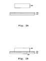
- FIG. 2A is a simplified schematic diagram illustrating a side view of a cleaning apparatus utilizing the single phase element in accordance with one embodiment of the invention.
- FIG. 2B is a simplified schematic diagram illustrating the lowering of the solid element to come into contact with the aqueous film and the substrate in accordance with one embodiment of the invention.
- FIG. 3A is a simplified schematic diagram illustrating a side view of a cleaning apparatus utilizing the single phase element in accordance with one embodiment of the invention.
- FIG. 3B is a top view of the cleaning apparatus of FIG. 3A in accordance with one embodiment of the invention.
- FIG. 4 is a simplified schematic diagram of an alternative embodiment for the single phase cleaning solid in accordance with one embodiment of the invention.
- FIG. 5A is another alternative embodiment where solid cleaning element is illustrated as a disc, in accordance with one embodiment of the invention.
- FIG. 5B is a simplified schematic diagram illustrating a side view of a element embodiment of the single phase cleaning element in accordance with one embodiment of the invention.
- FIG. 6 is a simplified schematic diagram illustrating further details on the activation layer for the single phase cleaning apparatus in accordance with one embodiment of the invention.
- FIG. 7 illustrates a more detailed schematic diagram of the ionization of region of FIG. 5 in accordance with one embodiment of the invention.
- FIG. 8 is a flow chart diagram illustrating the method operations for cleaning a substrate having surface contaminants in accordance with one embodiment of the invention.
- the embodiments described herein provide for a cleaning technique that reduces the abrasive contact and is efficient at cleaning contaminants from a semiconductor substrate which may contain high aspect ratio features. It should be appreciated that while the embodiments provide specific examples related to semiconductor cleaning applications, these cleaning applications may be extended to any technology requiring the removal of contaminants from a surface.
- the embodiments described herein move a single phase cleaning agent relative to a surface to be cleaned, where materials contained within the solid portion of the single phase cleaning agent provide lifting and removal of particles present on a wafer surface.
- a solid cleaning element is used as the single phase cleaning agent where the cleaning element has a substantially planar surface that is brought in contact with a surface of the substrate to be cleaned.
- the solid cleaning element may be referred to as a puck, bar, etc.
- the solid cleaning element is composed of a fatty acid, however, other materials may be used just as effectively. These other materials may include polymers, alkyl sulfonate, alkyl phosphate, alkyl phosphonate, biopolymers, proteins, etc.
- FIG. 1A is a simplified schematic diagram illustrating a high-level single phase cleaning operation in accordance with one embodiment of the invention.
- Solid cleaning element 100 is disposed over substrate 102 .
- Solid cleaning element 100 is composed of a carbon chain and may be selected from commonly known fatty acids, such as, myristic acid, palmitic acid, stearic acid, etc.
- the material for solid cleaning element 100 is a carbon chain having eight or more carbon atoms in the chain. It should be appreciated that with about ten or more carbon atoms, the chain will be a solid at room temperature.
- the solid cleaning element 100 may be composed of a carbon chain having less than eight carbons, and the solid cleaning element can be used in an environment lower than room temperature so that the composition is a solid.
- the mechanical properties of the solid cleaning element 100 are chosen such that the solid cleaning element has hardness less than the softest material on substrate 102 .
- the solid cleaning element 100 undergoes plastic deformation during contacting and relative motion between the solid cleaning element 100 and substrate 102 .
- plastic deformation refers to the point at which the solid cleaning element can no longer retain its shape and may also be referred to as plastic strain or plastic flow. Plastic deformation typically occurs under shear stress, as opposed to brittle fractures which occur under normal stress.
- Film 103 is then rinsed and removed. It should be appreciated that in one embodiment the solid cleaning element will interact with contaminants on the surface of substrate 102 and the contaminant are removed as thin film 103 is removed.
- FIG. 2A is a simplified schematic diagram illustrating a high-level single phase cleaning operation in accordance with one embodiment of the invention.
- Solid cleaning element 100 is disposed over substrate 102 .
- an activation layer 104 On a top surface of substrate 102 is an activation layer 104 .
- Activation layer 104 is a thin aqueous layer with a basic additive in one embodiment.
- the basic additive may be selected from the group consisting of ammonium hydroxide, sodium hydroxide, sodium hydroxide, potassium hydroxide, triethanol amine, or tetramethylammonium hydroxide in one embodiment. It should be appreciated that the basic additive is not limited to these compounds, as any base may be used to combine with the aqueous layer.
- Solid cleaning element 100 is composed of a carbon chain and may be selected from commonly known fatty acids, such as, myristic acid, palmitic acid, stearic acid, or alkysulphonates or alkyphosphonates, etc.
- the material for solid cleaning element 100 is a carbon chain having eight or more carbon atoms in the chain. It should be appreciated that with about ten or more carbon atoms, the chain will be a solid at room temperature.
- the solid cleaning element may be composed of a carbon chain having less than ten carbons, and the solid cleaning element can be used in an environment lower than room temperature so that the composition is a solid.
- activation layer 104 may be disposed over a top surface of substrate 102 through any commonly known means available. For example, activation layer can be poured onto substrate 102 , sprayed or other commonly available means.
- the element is a fatty acid
- the following are exemplary compounds that may be used to compose the element.
- aliphatic acids represent essentially any acid defined by organic compounds in which carbon atoms form open chains.
- a fatty acid is an example of an aliphatic acid that can be used as the solid cleaning material as discussed above.
- fatty acids examples include lauric, palmitic, stearic, oleic, linoleic, linolenic, arachidonic, gadoleic, eurcic, butyric, caproic, caprylic, myristic, margaric, behenic, lignoseric, myristoleic, palmitoleic, nervanic, parinaric, timnodonic, brassic, clupanodonic acid, lignoceric acid, cerotic acid, and mixtures thereof, among others.
- the solid cleaning element can represent a mixture of fatty acids defined by various carbon chain lengths extending from C-1 to about C-26.
- Carboxylic acids are defined by essentially any organic acid that includes one or more carboxyl groups (COOH).
- the carboxylic acids can include mixtures of various carbon chain lengths extending from C-1 through about C-100.
- the carboxylic acids can include other functional groups such as but not limited to methyl, vinyl, alkyne, amide, primary amine, secondary amine, tertiary amine, azo, nitrile, nitro, nitroso, pyridyl, peroxy, aldehyde, ketone, primary imine, secondary imine, ether, ester, halogen, isocyanate, isothiocyanate, phenyl, benzyl, phosphodiester, sulfhydryl.
- FIG. 2B is a simplified schematic diagram illustrating the lowering of the solid element to come into contact with the aqueous film and the substrate in accordance with one embodiment of the invention.
- Solid cleaning element 100 is lowered to contact activation layer 104 and a top surface of substrate 102 .
- the portion of solid cleaning element in contact with activation layer becomes ionized if the pH of activation layer is near the pKa of solid cleaning element.
- Activation layer 104 is at a pH above the pKa of the fatty acid in one embodiment. With regard to stearic acid, the pKa is approximately 10.2.
- activation layer 104 imbibes and diffuses into solid cleaning element swelling and changing the mechanical properties of solid cleaning element in region 106 relative to the remainder of solid cleaning element 100 .
- the dimensions of region 106 depend on the solid cleaning puck and activation layer material.
- region 106 is still considered as being a solid and element 100 may be thought of as a single phase, i.e., solid where region 106 is softer relative to a remainder of element 100 .
- a portion of region 106 is rubbed off and deposited on substrate 102 as a coating layer as discussed with regard to layer 103 of FIG. 1B .
- the coating layer is rinsed off substrate 102 removing the coating layer and any contamination on substrate 102 .
- activation layer 104 may be a surfactant/dispersant.
- the surfactant/dispersant will include ionic molecules.
- a surfactant such as ammonium dodecyl sulphate (ADS) is employed.
- ADS ammonium dodecyl sulphate
- any known nonionic, ionic or zwitterionic surfactant may be used.
- FIG. 3A is a simplified schematic diagram illustrating a side view of a cleaning apparatus utilizing the single phase element in accordance with one embodiment of the invention.
- Solid cleaning elements 118 a - 118 c are illustrated as elongated bars in this embodiment.
- Conveyor 110 which functions as a transport mechanism for the substrates is driven via rollers 112 and will support substrates to be cleaned with solid cleaning elements 118 a through 118 c .
- Activation layer 104 of FIG. 2 is provided for each substrate through reservoir 114 and delivered via nozzle 116 , although it is possible that the activation layer will not be applied. It should be appreciated that a nozzle and reservoir may correspond for each of solid cleaning elements 118 a through 118 c and is not shown for ease of illustration.
- Solid cleaning elements 118 a through 118 c can be translated in a vertical direction relative to substrate surfaces. It should be appreciated that a gimbaled technique may be used to support each of solid cleaning elements 118 a through 118 c.
- FIG. 3B is a top view of the cleaning apparatus of FIG. 3A in accordance with one embodiment of the invention.
- transport mechanism 110 supports substrates 102 a through 102 c .
- transport mechanism 110 is capable of clamping the substrate to support the substrate firmly and may also be capable of rotating the substrate.
- the element is lowered to contact the substrate.
- the activation layer has been applied to the substrate prior to contact, in order to clean the corresponding substrate.
- substrates 102 a through 102 c are cleaned as they traverse the path by the corresponding solid cleaning element 118 a through 118 c .
- each solid cleaning element may be different. That is, different fatty acids or other non-fatty acid material, and/or different activation agents may be used to provide sequential targeted cleaning. For example, a first element may target a certain type of contaminant, while the other elements can target other types of contaminants.
- FIG. 4 is a simplified schematic diagram of an alternative embodiment for the single phase cleaning solid in accordance with one embodiment of the invention.
- the single phase cleaning solid is a roller.
- the roller will rotate around axis 130 .
- roller 118 d may be applied to any of the embodiments described herein.
- support structure 131 may be used to force a surface of roller 118 d against a wafer surface.
- a shaft may traverse through roller 118 d along axis 130 .
- support structure 131 may be held at different angles relative to a planar surface of a wafer being cleaned.
- support structure 131 may be coupled to roller 118 d through known techniques that allows for free rotation of roller 118 d and accommodates the angular movement mentioned above.
- FIG. 5A is another alternative embodiment where solid cleaning element is illustrated as a disc.
- Disc 118 e rotates relative to the rotation of substrate 102 in order to clean the surface of substrate 102 .
- disc 118 e may be various diameters relative to the substrate 102 being cleaned and the relative diameters are exemplary illustrations not meant to be limiting.
- substrate 102 and disc 118 e may rotate in similar directions, or disc 118 e and substrate 102 may rotate in opposite directions.
- a gimbaled support structure may be incorporated with element 118 e.
- FIG. 5B is a simplified schematic diagram illustrating a side view of a element embodiment of the single phase cleaning element in accordance with one embodiment of the invention.
- Element 118 e is affixed to support structure 131 .
- Element 118 e may be affixed to support structure 131 through adhesive or mechanical means where the support structure is structurally integrated with the element through known means.
- element 118 e is defined around support 140 to provide the structural support.
- element 118 e can be thought of as being molded around support 140 .
- Support structure 131 provides rotational support of element 118 e .
- support 131 may be gimbaled as discussed above.
- Reservoir 114 provides activation fluid through delivery line 116 to form activation layer 104 on a top surface of wafer 102 .
- the activation layer is applied prior to contacting of element 118 e with the surface to be cleaned.
- the substrate and cleaning element in contact with the activation layer ionizes preventing adsorption of solid cleaning element to substrate.
- Element 118 e and/or wafer 102 are rotated to perform the cleaning operation. It should be appreciated that element 118 e remains as a solid however, the physical properties, i.e., the hardness of the top portion 118 e - 1 relative to the hardness of the bottom portion 118 e - 2 is altered by the activation layer 104 at the bottom surface of element 118 e .
- the embodiments described herein provide a solid surface that does not have the holes/cavities of a typical brush applied to clean the surface of wafer 102 .
- the embodiments described herein provide a contiguous uninterrupted cleaning layer that may conform to the surface of wafer 102 .
- the activation of bottom portion 118 e - 1 provides a softer interface in which pressure exerted on top portion 118 e - 2 is translated to provide the cleansing action.
- FIG. 6 is a simplified schematic diagram illustrating further details on the activation layer for the single phase cleaning apparatus in accordance with one embodiment of the invention.
- Substrate 102 has activation layer 104 disposed thereon, and as solid cleaning element 100 is brought into contact with activation layer 104 , water imbibes into solid cleaning element 100 . The water penetrates into the grain structure of the solid cleaning element 100 as illustrated in region 106 .
- activation layer 104 is an aqueous layer in one embodiment where the pH of the aqueous layer is basic in order to ionize and neutralize the fatty acid in region 106 . In essence, the penetration of the activation layer into region 106 alters the properties of solid cleaning element 100 in that region.
- region 106 solid cleaning element 100 may become gelatinous in nature but still in solid phase.
- FIG. 7 the ionization of region 106 is illustrated.
- the hydrogen atoms of the carboxylic acid groups dissociate resulting in a negative charged functional group at this interface in region 106 .
- absorption to a negatively charged interface will be prevented. That is, the solid cleaning element will not adhere to the wafer surface thereby ensuring efficient cleaning is achieved.
- the activation layer is a surfactant/dispersant, the effect described above with regard to FIG. 6 is achieved.
- the activation layer has chemical additives to enhance contamination removal. These chemical additives include hydrofluoric acid, sulfuric acid, hydrochloric acid, tetramethyl ammonium hydroxide, hydrogen peroxide, among others.
- FIG. 8 is a flow chart diagram illustrating the method operations for cleaning a substrate having surface contaminants in accordance with one embodiment of the invention.
- the method initiates with operation 200 where an activation solution is applied to the surface of the substrate through operation can proceed without application of the activation surface.
- the activation solution may be an aqueous solution which has a pH that is greater than a pKa of a cleaning apparatus.
- the activation solution may be a surfactant. It should be appreciated that the activation solution may be poured onto the substrate or sprayed or any other means currently available.
- the method then advances to operation 202 where a solid cleaning surface is brought into contact with the activation solution and the surface of the substrate.
- Bringing the solid cleaning surface into contact with the activation solution results in activating or ionizing/neutralizing a portion of the solid cleaning surface as illustrated with reference to FIGS. 6 and 7 and as specified in operation 204 .
- This ionization/neutralization or activation prevents absorption to ensure that the solid cleaning element will not leave behind any residue.
- the surfactant prevents absorption to ensure that the solid cleaning element will not leave behind any residue.
- the cleaning element is a disk, such as in FIGS. 5A and 5B
- one exemplary configuration of the element may be a disk with dimensions of 5 inches in diameter and a height or depth of one inch.
- the portion of the 1 inch depth is about 1 ⁇ 8 of an inch.
- the activation solution is absorbed into a portion of the solid cleaning element as described with reference to FIGS. 5 and 6 .
- the method of FIG. 8 advances to operation 206 where the substrate and/or the solid cleaning surface is moved relative to each other to clean the surface of the substrate.
- the solid cleaning surface may rotate, roll, slide, etc., relative to the surface of the substrate to be cleaned.
- the solid cleaning surface can be a disc, bar, puck, roller, or any other suitable apparatus for applying the functionality described herein to the surface of the wafer for cleaning.
- any geometric shape that may leave a layer on the surface of the substrate through plastic deformation or any geometric shape that may interact with the activation layer to remove surface contaminants may be employed with the embodiments described herein.
- the support structure provided for the solid cleaning surface may include a gimbaled structure to allow rotation of the solid cleaning surface in multiple dimensions, such as a two axis gimbal.
- a gimbal is typically made up of two or three pairs of pivots mounted on axes at right angles.
- the present invention has been described in the context of removing contaminants from a semiconductor wafer, it should be understood that the previously described principles and techniques of the present invention can be equally applied to cleaning surfaces other than semiconductor wafers.
- the present invention can be used to clean any equipment surface used in semiconductor manufacturing, wherein any equipment surface refers to any surface that is in environmental communication with the wafer, e.g., shares air space with the wafer.
- the present invention can also be used in other technology areas where contamination removal is important.
- the present invention can be used to remove contamination on parts used in the space program, or other high technology areas such as surface science, energy, optics, microelectronics, MEMS, flat-panel processing, solar cells, memory devices, etc.
- the aforementioned listing of exemplary areas where the present invention may be used is not intended to represent an inclusive listing.
- the wafer as used in the exemplary description herein can be generalized to represent essentially any other structure, such as a substrate, a part, a panel, etc.
Landscapes
- Chemical & Material Sciences (AREA)
- Organic Chemistry (AREA)
- Chemical Kinetics & Catalysis (AREA)
- Engineering & Computer Science (AREA)
- Oil, Petroleum & Natural Gas (AREA)
- Life Sciences & Earth Sciences (AREA)
- Wood Science & Technology (AREA)
- Mechanical Engineering (AREA)
- Metallurgy (AREA)
- Materials Engineering (AREA)
- General Chemical & Material Sciences (AREA)
- Inorganic Chemistry (AREA)
- Physics & Mathematics (AREA)
- General Physics & Mathematics (AREA)
- Cleaning Or Drying Semiconductors (AREA)
Priority Applications (11)
| Application Number | Priority Date | Filing Date | Title |
|---|---|---|---|
| US11/612,352 US8316866B2 (en) | 2003-06-27 | 2006-12-18 | Method and apparatus for cleaning a semiconductor substrate |
| EP06846809A EP1965933A2 (de) | 2005-12-30 | 2006-12-26 | Verfahren und vorrichtung zur reinigung eines halbleitersubstrats |
| PCT/US2006/062604 WO2007079373A2 (en) | 2005-12-30 | 2006-12-26 | Method and apparatus for cleaning a semiconductor substrate |
| CN2006800534252A CN101389414B (zh) | 2005-12-30 | 2006-12-26 | 清洁半导体基片的方法和装置 |
| KR1020137009228A KR20130042061A (ko) | 2005-12-30 | 2006-12-26 | 반도체 기판을 세정하는 방법 및 장치 |
| KR1020087018880A KR101401753B1 (ko) | 2005-12-30 | 2006-12-26 | 반도체 기판을 세정하는 방법 및 장치 |
| JP2008548829A JP5237825B2 (ja) | 2005-12-30 | 2006-12-26 | 半導体基板を洗浄する方法および装置 |
| TW096100024A TWI335247B (en) | 2005-12-30 | 2007-01-02 | Method and apparatus for cleaning a semiconductor substrate |
| US13/661,929 US8591662B2 (en) | 2005-12-30 | 2012-10-26 | Methods for cleaning a semiconductor substrate |
| JP2012242490A JP5518163B2 (ja) | 2005-12-30 | 2012-11-02 | 半導体基板を洗浄する方法および装置 |
| US14/055,850 US20140059789A1 (en) | 2005-12-30 | 2013-10-16 | Apparatus for Cleaning a Semiconductor Substrate |
Applications Claiming Priority (3)
| Application Number | Priority Date | Filing Date | Title |
|---|---|---|---|
| US10/608,871 US20040261823A1 (en) | 2003-06-27 | 2003-06-27 | Method and apparatus for removing a target layer from a substrate using reactive gases |
| US75537705P | 2005-12-30 | 2005-12-30 | |
| US11/612,352 US8316866B2 (en) | 2003-06-27 | 2006-12-18 | Method and apparatus for cleaning a semiconductor substrate |
Related Parent Applications (1)
| Application Number | Title | Priority Date | Filing Date |
|---|---|---|---|
| US10/608,871 Continuation-In-Part US20040261823A1 (en) | 2003-06-27 | 2003-06-27 | Method and apparatus for removing a target layer from a substrate using reactive gases |
Related Child Applications (1)
| Application Number | Title | Priority Date | Filing Date |
|---|---|---|---|
| US13/661,929 Division US8591662B2 (en) | 2005-12-30 | 2012-10-26 | Methods for cleaning a semiconductor substrate |
Publications (2)
| Publication Number | Publication Date |
|---|---|
| US20070084483A1 US20070084483A1 (en) | 2007-04-19 |
| US8316866B2 true US8316866B2 (en) | 2012-11-27 |
Family
ID=38228934
Family Applications (3)
| Application Number | Title | Priority Date | Filing Date |
|---|---|---|---|
| US11/612,352 Expired - Fee Related US8316866B2 (en) | 2003-06-27 | 2006-12-18 | Method and apparatus for cleaning a semiconductor substrate |
| US13/661,929 Expired - Fee Related US8591662B2 (en) | 2005-12-30 | 2012-10-26 | Methods for cleaning a semiconductor substrate |
| US14/055,850 Abandoned US20140059789A1 (en) | 2005-12-30 | 2013-10-16 | Apparatus for Cleaning a Semiconductor Substrate |
Family Applications After (2)
| Application Number | Title | Priority Date | Filing Date |
|---|---|---|---|
| US13/661,929 Expired - Fee Related US8591662B2 (en) | 2005-12-30 | 2012-10-26 | Methods for cleaning a semiconductor substrate |
| US14/055,850 Abandoned US20140059789A1 (en) | 2005-12-30 | 2013-10-16 | Apparatus for Cleaning a Semiconductor Substrate |
Country Status (5)
| Country | Link |
|---|---|
| US (3) | US8316866B2 (de) |
| EP (1) | EP1965933A2 (de) |
| JP (1) | JP5518163B2 (de) |
| KR (1) | KR20130042061A (de) |
| WO (1) | WO2007079373A2 (de) |
Cited By (3)
| Publication number | Priority date | Publication date | Assignee | Title |
|---|---|---|---|---|
| US20130037051A1 (en) * | 2011-08-04 | 2013-02-14 | Georg Eitelhuber | Apparatuses, Systems and Methods for Cleaning Photovoltaic Devices |
| US9919939B2 (en) | 2011-12-06 | 2018-03-20 | Delta Faucet Company | Ozone distribution in a faucet |
| US11458214B2 (en) | 2015-12-21 | 2022-10-04 | Delta Faucet Company | Fluid delivery system including a disinfectant device |
Families Citing this family (8)
| Publication number | Priority date | Publication date | Assignee | Title |
|---|---|---|---|---|
| US8316866B2 (en) * | 2003-06-27 | 2012-11-27 | Lam Research Corporation | Method and apparatus for cleaning a semiconductor substrate |
| US7981221B2 (en) * | 2008-02-21 | 2011-07-19 | Micron Technology, Inc. | Rheological fluids for particle removal |
| US8105997B2 (en) * | 2008-11-07 | 2012-01-31 | Lam Research Corporation | Composition and application of a two-phase contaminant removal medium |
| JP2013133458A (ja) * | 2011-12-27 | 2013-07-08 | Idemitsu Kosan Co Ltd | 水性洗浄剤 |
| JP5820404B2 (ja) * | 2013-02-05 | 2015-11-24 | 株式会社東芝 | 平坦化方法及び平坦化装置 |
| CN106605291B (zh) | 2014-09-11 | 2020-05-05 | 株式会社德山 | 氮化铝单结晶基板的洗净方法及层叠体 |
| US20170312791A1 (en) * | 2014-11-24 | 2017-11-02 | Corning Incorporated | Method and apparatus for substrate surface cleaning |
| US9570285B2 (en) * | 2015-04-17 | 2017-02-14 | Taiwan Semiconductor Manufacturing Company, Ltd. | Cleaning composition and methods thereof |
Citations (135)
| Publication number | Priority date | Publication date | Assignee | Title |
|---|---|---|---|---|
| US3037887A (en) | 1959-05-04 | 1962-06-05 | Dow Chemical Co | Foam cleaning of surfaces |
| US3212762A (en) | 1960-05-23 | 1965-10-19 | Dow Chemical Co | Foam generator |
| US3436262A (en) | 1964-09-25 | 1969-04-01 | Dow Chemical Co | Cleaning by foam contact,and foam regeneration method |
| US3617095A (en) | 1967-10-18 | 1971-11-02 | Petrolite Corp | Method of transporting bulk solids |
| US3978176A (en) | 1972-09-05 | 1976-08-31 | Minnesota Mining And Manufacturing Company | Sparger |
| US4085059A (en) | 1974-05-02 | 1978-04-18 | Bunker Ramo Corporation | Foam type coating remover |
| US4133773A (en) | 1977-07-28 | 1979-01-09 | The Dow Chemical Company | Apparatus for making foamed cleaning solutions and method of operation |
| US4156619A (en) | 1975-06-11 | 1979-05-29 | Wacker-Chemitronic Gesellschaft Fur Elektronik-Grundstoffe Mbh | Process for cleaning semi-conductor discs |
| US4238244A (en) | 1978-10-10 | 1980-12-09 | Halliburton Company | Method of removing deposits from surfaces with a gas agitated cleaning liquid |
| US4781764A (en) | 1986-07-28 | 1988-11-01 | U.S. Philips Corporation | Method of removing undesired particles from a surface of a substrate |
| US4817652A (en) | 1987-03-26 | 1989-04-04 | Regents Of The University Of Minnesota | System for surface and fluid cleaning |
| US4838289A (en) | 1982-08-03 | 1989-06-13 | Texas Instruments Incorporated | Apparatus and method for edge cleaning |
| US4849027A (en) | 1987-04-16 | 1989-07-18 | Simmons Bobby G | Method for recycling foamed solvents |
| US4911761A (en) | 1984-05-21 | 1990-03-27 | Cfm Technologies Research Associates | Process and apparatus for drying surfaces |
| US4962776A (en) | 1987-03-26 | 1990-10-16 | Regents Of The University Of Minnesota | Process for surface and fluid cleaning |
| US5000795A (en) | 1989-06-16 | 1991-03-19 | At&T Bell Laboratories | Semiconductor wafer cleaning method and apparatus |
| US5048549A (en) | 1988-03-02 | 1991-09-17 | General Dynamics Corp., Air Defense Systems Div. | Apparatus for cleaning and/or fluxing circuit card assemblies |
| US5102777A (en) | 1990-02-01 | 1992-04-07 | Ardrox Inc. | Resist stripping |
| US5105556A (en) | 1987-08-12 | 1992-04-21 | Hitachi, Ltd. | Vapor washing process and apparatus |
| US5113597A (en) | 1986-07-08 | 1992-05-19 | Kohlensaeurewerk Deutschland Gmbh | Process for drying of plant or animal material |
| DE4038587A1 (de) | 1990-12-04 | 1992-06-11 | Hamatech Halbleiter Maschinenb | Transportvorrichtung fuer substrate |
| US5175124A (en) | 1991-03-25 | 1992-12-29 | Motorola, Inc. | Process for fabricating a semiconductor device using re-ionized rinse water |
| US5181985A (en) | 1988-06-01 | 1993-01-26 | Wacker-Chemitronic Gesellschaft Fur Elektronik-Grundstoffe Mbh | Process for the wet-chemical surface treatment of semiconductor wafers |
| US5226969A (en) | 1990-03-07 | 1993-07-13 | Hitachi, Ltd. | Method for cleaning solid surface with a mixture of pure water and calcium carbonate particles |
| US5242669A (en) | 1992-07-09 | 1993-09-07 | The S. A. Day Mfg. Co., Inc. | High purity potassium tetrafluoroaluminate and method of making same |
| US5271774A (en) | 1990-03-01 | 1993-12-21 | U.S. Philips Corporation | Method for removing in a centrifuge a liquid from a surface of a substrate |
| US5288332A (en) | 1993-02-05 | 1994-02-22 | Honeywell Inc. | A process for removing corrosive by-products from a circuit assembly |
| US5306350A (en) | 1990-12-21 | 1994-04-26 | Union Carbide Chemicals & Plastics Technology Corporation | Methods for cleaning apparatus using compressed fluids |
| US5336371A (en) | 1993-03-18 | 1994-08-09 | At&T Bell Laboratories | Semiconductor wafer cleaning and rinsing techniques using re-ionized water and tank overflow |
| US5415191A (en) | 1991-01-28 | 1995-05-16 | Kabushiki Kaisha Toshiba | Arrangement for cleaning semiconductor wafers using mixer |
| US5417768A (en) | 1993-12-14 | 1995-05-23 | Autoclave Engineers, Inc. | Method of cleaning workpiece with solvent and then with liquid carbon dioxide |
| US5464480A (en) | 1993-07-16 | 1995-11-07 | Legacy Systems, Inc. | Process and apparatus for the treatment of semiconductor wafers in a fluid |
| US5472502A (en) | 1993-08-30 | 1995-12-05 | Semiconductor Systems, Inc. | Apparatus and method for spin coating wafers and the like |
| US5494526A (en) | 1994-04-08 | 1996-02-27 | Texas Instruments Incorporated | Method for cleaning semiconductor wafers using liquified gases |
| US5498293A (en) | 1994-06-23 | 1996-03-12 | Mallinckrodt Baker, Inc. | Cleaning wafer substrates of metal contamination while maintaining wafer smoothness |
| US5656097A (en) | 1993-10-20 | 1997-08-12 | Verteq, Inc. | Semiconductor wafer cleaning system |
| US5660642A (en) | 1995-05-26 | 1997-08-26 | The Regents Of The University Of California | Moving zone Marangoni drying of wet objects using naturally evaporated solvent vapor |
| US5674831A (en) | 1993-12-30 | 1997-10-07 | Ecolab Inc. | Method of making urea-based solid cleaning compositions |
| US5705223A (en) | 1994-07-26 | 1998-01-06 | International Business Machine Corp. | Method and apparatus for coating a semiconductor wafer |
| US5800626A (en) | 1997-02-18 | 1998-09-01 | International Business Machines Corporation | Control of gas content in process liquids for improved megasonic cleaning of semiconductor wafers and microelectronics substrates |
| US5858283A (en) | 1996-11-18 | 1999-01-12 | Burris; William Alan | Sparger |
| EP0905746A1 (de) | 1997-09-24 | 1999-03-31 | Interuniversitair Micro-Elektronica Centrum Vzw | Verfahren zum Entfernen einer Flüssigkeit von einer Oberfläche einer umlaufenden Substrat |
| US5900191A (en) | 1997-01-14 | 1999-05-04 | Stable Air, Inc. | Foam producing apparatus and method |
| US5904156A (en) | 1997-09-24 | 1999-05-18 | International Business Machines Corporation | Dry film resist removal in the presence of electroplated C4's |
| US5911837A (en) | 1993-07-16 | 1999-06-15 | Legacy Systems, Inc. | Process for treatment of semiconductor wafers in a fluid |
| US5932493A (en) | 1997-09-15 | 1999-08-03 | International Business Machines Corporaiton | Method to minimize watermarks on silicon substrates |
| US5945351A (en) | 1996-05-31 | 1999-08-31 | Siemens Aktiengesellschaft | Method for etching damaged zones on an edge of a semiconductor substrate, and etching system |
| US5944582A (en) | 1993-11-16 | 1999-08-31 | Applied Materials, Inc. | Chemical mechanical polishing with a small polishing pad |
| US5944581A (en) | 1998-07-13 | 1999-08-31 | Ford Motor Company | CO2 cleaning system and method |
| US5951779A (en) | 1997-07-09 | 1999-09-14 | Ses Co., Ltd. | Treatment method of semiconductor wafers and the like and treatment system for the same |
| US5964958A (en) | 1995-06-07 | 1999-10-12 | Gary W. Ferrell | Methods for drying and cleaning objects using aerosols |
| US5964954A (en) | 1993-11-05 | 1999-10-12 | Tokyo Electron Limited | Double-sided substrate cleaning apparatus and cleaning method using the same |
| US5968285A (en) | 1995-06-07 | 1999-10-19 | Gary W. Ferrell | Methods for drying and cleaning of objects using aerosols and inert gases |
| US5997653A (en) | 1996-10-07 | 1999-12-07 | Tokyo Electron Limited | Method for washing and drying substrates |
| US6048409A (en) | 1995-05-26 | 2000-04-11 | Mitsubishi Denki Kabushiki Kaisha | Washing apparatus and washing method |
| US6049996A (en) | 1998-07-10 | 2000-04-18 | Ball Semiconductor, Inc. | Device and fluid separator for processing spherical shaped devices |
| US6081650A (en) | 1994-06-30 | 2000-06-27 | Thomson Licensing S.A. | Transport processor interface and video recorder/playback apparatus in a field structured datastream suitable for conveying television information |
| US6090217A (en) | 1998-12-09 | 2000-07-18 | Kittle; Paul A. | Surface treatment of semiconductor substrates |
| US6092538A (en) | 1996-09-25 | 2000-07-25 | Shuzurifuresher Kaihatsukyodokumiai | Method for using high density compressed liquefied gases in cleaning applications |
| US6152805A (en) | 1997-07-17 | 2000-11-28 | Canon Kabushiki Kaisha | Polishing machine |
| US6158445A (en) | 1993-10-20 | 2000-12-12 | Olesen; Michael B. | Semiconductor wafer cleaning method |
| US6167583B1 (en) | 1997-05-15 | 2001-01-02 | Kabushiki Kaisha Toshiba | Double side cleaning apparatus for semiconductor substrate |
| JP2001064688A (ja) | 1999-06-23 | 2001-03-13 | Jsr Corp | 半導体部品用洗浄剤、半導体部品の洗浄方法、研磨用組成物、および研磨方法 |
| US6228563B1 (en) | 1999-09-17 | 2001-05-08 | Gasonics International Corporation | Method and apparatus for removing post-etch residues and other adherent matrices |
| US6267125B1 (en) | 1997-05-09 | 2001-07-31 | Semitool, Inc. | Apparatus and method for processing the surface of a workpiece with ozone |
| US6270584B1 (en) | 1997-12-03 | 2001-08-07 | Gary W. Ferrell | Apparatus for drying and cleaning objects using controlled aerosols and gases |
| US6272712B1 (en) | 1999-04-02 | 2001-08-14 | Lam Research Corporation | Brush box containment apparatus |
| US6276459B1 (en) | 2000-02-01 | 2001-08-21 | Bradford James Herrick | Compressed air foam generator |
| US6286231B1 (en) | 2000-01-12 | 2001-09-11 | Semitool, Inc. | Method and apparatus for high-pressure wafer processing and drying |
| US6290780B1 (en) | 1999-03-19 | 2001-09-18 | Lam Research Corporation | Method and apparatus for processing a wafer |
| US20010037818A1 (en) * | 2000-05-02 | 2001-11-08 | Riichiro Harano | Sherbet-like cleaning composition and method and system for cleaning substrate |
| US6319801B1 (en) | 1997-11-28 | 2001-11-20 | Nec Corporation | Method for cleaning a substrate and cleaning solution |
| US6352082B1 (en) | 1994-11-14 | 2002-03-05 | Scd Mountain View | Ultra-low particle semiconductor cleaner |
| US6386956B1 (en) | 1998-11-05 | 2002-05-14 | Sony Corporation | Flattening polishing device and flattening polishing method |
| US6398975B1 (en) | 1997-09-24 | 2002-06-04 | Interuniversitair Microelektronica Centrum (Imec) | Method and apparatus for localized liquid treatment of the surface of a substrate |
| US6401734B1 (en) | 1999-03-11 | 2002-06-11 | Hitachi Kokusai Electric Inc. | Substrate treating apparatus |
| US20020072482A1 (en) | 2000-12-07 | 2002-06-13 | Sachdev Krishna G. | Polycarboxylates-based aqueous compositions for cleaning of screening apparatus |
| US20020094684A1 (en) | 2000-11-27 | 2002-07-18 | Hirasaki George J. | Foam cleaning process in semiconductor manufacturing |
| US6423148B1 (en) | 1998-09-07 | 2002-07-23 | Nec Corporation | Substrate-cleaning method and substrate-cleaning solution |
| US20020121290A1 (en) | 1999-08-25 | 2002-09-05 | Applied Materials, Inc. | Method and apparatus for cleaning/drying hydrophobic wafers |
| JP2002280330A (ja) | 2001-03-21 | 2002-09-27 | Lintec Corp | チップ状部品のピックアップ方法 |
| US6457199B1 (en) | 2000-10-12 | 2002-10-01 | Lam Research Corporation | Substrate processing in an immersion, scrub and dry system |
| US6467897B1 (en) * | 2001-01-08 | 2002-10-22 | 3M Innovative Properties Company | Energy curable inks and other compositions incorporating surface modified, nanometer-sized particles |
| JP2002309638A (ja) | 2001-04-17 | 2002-10-23 | Takiron Co Ltd | 建物の排水管路における通気性掃除口 |
| US20020160608A1 (en) | 1998-10-07 | 2002-10-31 | Kabushiki Kaisha Toshiba | Copper-based metal polishing composition, method for manufacturing a semiconductor device, polishing composition, aluminum-based metal polishing composition, and tungsten-based metal polishing composition |
| US6491764B2 (en) | 1997-09-24 | 2002-12-10 | Interuniversitair Microelektronics Centrum (Imec) | Method and apparatus for removing a liquid from a surface of a rotating substrate |
| US20020185164A1 (en) | 2001-03-15 | 2002-12-12 | Nec Corporation | Apparatus for applying cleaning treatment to the surface of a processed member |
| US6493902B2 (en) | 2001-02-22 | 2002-12-17 | Chung-Yi Lin | Automatic wall cleansing apparatus |
| US6514921B1 (en) | 1996-06-05 | 2003-02-04 | Wako Pure Chemical Industries, Ltd. | Cleaning agent |
| US6513538B2 (en) | 2000-07-18 | 2003-02-04 | Samsung Electronics Co., Ltd. | Method of removing contaminants from integrated circuit substrates using cleaning solutions |
| US6527870B2 (en) | 2000-10-05 | 2003-03-04 | Lam Research Corporation | Wafer cleaning module and method for cleaning the surface of a substrate |
| US6532976B1 (en) | 1995-07-10 | 2003-03-18 | Lg Semicon Co., Ltd. | Semiconductor wafer cleaning apparatus |
| US6537915B2 (en) | 1999-09-02 | 2003-03-25 | Micron Technology, Inc. | Methods of treating surfaces of substrates |
| US20030075204A1 (en) | 2000-06-30 | 2003-04-24 | Lam Research Corporation | Methods for wafer proximity cleaning and drying |
| US6562726B1 (en) | 1999-06-29 | 2003-05-13 | Micron Technology, Inc. | Acid blend for removing etch residue |
| US6576066B1 (en) | 1999-12-06 | 2003-06-10 | Nippon Telegraph And Telephone Corporation | Supercritical drying method and supercritical drying apparatus |
| US6594847B1 (en) | 2000-03-28 | 2003-07-22 | Lam Research Corporation | Single wafer residue, thin film removal and clean |
| US6602111B1 (en) * | 1999-07-16 | 2003-08-05 | Seimi Chemical Co., Ltd. | Abrasive |
| US20030148903A1 (en) | 2001-11-19 | 2003-08-07 | Unilever Home & Personal Care Usa, Division Of Conopco, Inc. | Washing system |
| EP0989600A3 (de) | 1998-09-25 | 2003-09-10 | Sumitomo Electric Industries, Ltd. | Oberflächenreinigungsverfahren zur Herstellung von epitaktischen II-VI Verbindungshalbleiterscheiben |
| US20030171239A1 (en) | 2002-01-28 | 2003-09-11 | Patel Bakul P. | Methods and compositions for chemically treating a substrate using foam technology |
| EP0827188B1 (de) | 1996-08-09 | 2003-09-17 | Mitsubishi Gas Chemical Company, Inc. | Reinigungsflüssigkeit für die Herstellung von Halbleiter-Anordnungen und Verfahren zur Herstellung von Halbleiter-Anordnungen unter Verwendung derselben |
| JP2003282513A (ja) | 2002-03-26 | 2003-10-03 | Seiko Epson Corp | 有機物剥離方法及び有機物剥離装置 |
| US20030226577A1 (en) | 2002-04-16 | 2003-12-11 | Takehiko Orll | Liquid processing apparatus and liquid processing method |
| US20040002430A1 (en) | 2002-07-01 | 2004-01-01 | Applied Materials, Inc. | Using a time critical wafer cleaning solution by combining a chelating agent with an oxidizer at point-of-use |
| US20040053808A1 (en) | 2000-05-17 | 2004-03-18 | Wilfried Raehse | Washing or cleaning agent shaped bodies |
| US20040065352A1 (en) | 2002-07-11 | 2004-04-08 | Ryosuke Yonekura | Cleaning apparatus and cleaning method |
| US6733596B1 (en) | 2002-12-23 | 2004-05-11 | Lam Research Corporation | Substrate cleaning brush preparation sequence, method, and system |
| US20040099290A1 (en) | 2001-05-22 | 2004-05-27 | Mitsubishi Chemical Corporation | Method for cleaning a surface of a substrate |
| US20040134515A1 (en) | 1999-10-29 | 2004-07-15 | Castrucci Paul P. | Apparatus and method for semiconductor wafer cleaning |
| US20040159335A1 (en) | 2002-05-17 | 2004-08-19 | P.C.T. Systems, Inc. | Method and apparatus for removing organic layers |
| US20040163681A1 (en) | 2003-02-25 | 2004-08-26 | Applied Materials, Inc. | Dilute sulfuric peroxide at point-of-use |
| US6787473B2 (en) | 2001-03-27 | 2004-09-07 | Micron Technology, Inc. | Post-planarization clean-up |
| US6802911B2 (en) | 2001-09-19 | 2004-10-12 | Samsung Electronics Co., Ltd. | Method for cleaning damaged layers and polymer residue from semiconductor device |
| US20040223166A1 (en) | 1999-12-13 | 2004-11-11 | Toshifumi Kimba | Substrate film thickness measurement method, substrate film thickness measurement apparatus and substrate processing apparatus |
| US20040261823A1 (en) | 2003-06-27 | 2004-12-30 | Lam Research Corporation | Method and apparatus for removing a target layer from a substrate using reactive gases |
| US6846380B2 (en) | 2002-06-13 | 2005-01-25 | The Boc Group, Inc. | Substrate processing apparatus and related systems and methods |
| US20050045209A1 (en) | 2000-08-11 | 2005-03-03 | Samantha Tan | System and method for cleaning semicondutor fabrication equipment parts |
| US6874516B2 (en) | 2001-05-31 | 2005-04-05 | m•FSI Ltd. | Substrate cleaning apparatus |
| US6896826B2 (en) | 1997-01-09 | 2005-05-24 | Advanced Technology Materials, Inc. | Aqueous cleaning composition containing copper-specific corrosion inhibitor for cleaning inorganic residues on semiconductor substrate |
| US20050132515A1 (en) | 2003-12-18 | 2005-06-23 | Lam Research Corporation | Proximity brush unit apparatus and method |
| US20050133061A1 (en) | 2003-12-23 | 2005-06-23 | Lam Research Corporation | Apparatuses and methods for cleaning a substrate |
| JP2005194294A (ja) | 2003-12-26 | 2005-07-21 | Nec Electronics Corp | 洗浄液及び半導体装置の製造方法 |
| US20050159322A1 (en) | 2003-11-07 | 2005-07-21 | Chang-Sup Min | Aqueous cleaning solution for integrated circuit device and method of cleaning using the cleaning solution |
| US6927176B2 (en) | 2000-06-26 | 2005-08-09 | Applied Materials, Inc. | Cleaning method and solution for cleaning a wafer in a single wafer process |
| US20050176606A1 (en) | 2004-02-10 | 2005-08-11 | Jsr Corporation | Cleaning composition, method for cleaning semiconductor substrate, and process for manufacturing semiconductor device |
| US20050183740A1 (en) | 2004-02-19 | 2005-08-25 | Fulton John L. | Process and apparatus for removing residues from semiconductor substrates |
| US6946396B2 (en) | 2003-10-30 | 2005-09-20 | Nissan Chemical Indusries, Ltd. | Maleic acid and ethylene urea containing formulation for removing residue from semiconductor substrate and method for cleaning wafer |
| US6951042B1 (en) | 2003-02-28 | 2005-10-04 | Lam Research Corporation | Brush scrubbing-high frequency resonating wafer processing system and methods for making and implementing the same |
| US20060201267A1 (en) | 2005-01-25 | 2006-09-14 | Schukra Of North America, Ltd. | Multiple turn mechanism for manual lumbar support adjustment |
| US7122126B1 (en) | 2000-09-28 | 2006-10-17 | Materials And Technologies Corporation | Wet processing using a fluid meniscus, apparatus and method |
| US20060283486A1 (en) | 2005-06-15 | 2006-12-21 | Lam Research Corporation | Method and apparatus for cleaning a substrate using non-newtonian fluids |
| US20060285930A1 (en) | 2005-06-15 | 2006-12-21 | Lam Research Corporation | Method and apparatus for transporting a substrate using non-Newtonian fluid |
| US20070000518A1 (en) | 2005-06-30 | 2007-01-04 | Lam Research Corporation | Method for removing material from semiconductor wafer and apparatus for performing the same |
| US20070084483A1 (en) * | 2003-06-27 | 2007-04-19 | Freer Erik M | Method and apparatus for cleaning a semiconductor substrate |
Family Cites Families (2)
| Publication number | Priority date | Publication date | Assignee | Title |
|---|---|---|---|---|
| MY114512A (en) * | 1992-08-19 | 2002-11-30 | Rodel Inc | Polymeric substrate with polymeric microelements |
| US6091217A (en) * | 1998-01-29 | 2000-07-18 | Elite Access Systems, Inc. | Safety gate operator which prevents entrapment, and method of its operation |
-
2006
- 2006-12-18 US US11/612,352 patent/US8316866B2/en not_active Expired - Fee Related
- 2006-12-26 KR KR1020137009228A patent/KR20130042061A/ko not_active Abandoned
- 2006-12-26 WO PCT/US2006/062604 patent/WO2007079373A2/en not_active Ceased
- 2006-12-26 EP EP06846809A patent/EP1965933A2/de not_active Withdrawn
-
2012
- 2012-10-26 US US13/661,929 patent/US8591662B2/en not_active Expired - Fee Related
- 2012-11-02 JP JP2012242490A patent/JP5518163B2/ja not_active Expired - Fee Related
-
2013
- 2013-10-16 US US14/055,850 patent/US20140059789A1/en not_active Abandoned
Patent Citations (145)
| Publication number | Priority date | Publication date | Assignee | Title |
|---|---|---|---|---|
| US3037887A (en) | 1959-05-04 | 1962-06-05 | Dow Chemical Co | Foam cleaning of surfaces |
| US3212762A (en) | 1960-05-23 | 1965-10-19 | Dow Chemical Co | Foam generator |
| US3436262A (en) | 1964-09-25 | 1969-04-01 | Dow Chemical Co | Cleaning by foam contact,and foam regeneration method |
| US3617095A (en) | 1967-10-18 | 1971-11-02 | Petrolite Corp | Method of transporting bulk solids |
| US3978176A (en) | 1972-09-05 | 1976-08-31 | Minnesota Mining And Manufacturing Company | Sparger |
| US4085059A (en) | 1974-05-02 | 1978-04-18 | Bunker Ramo Corporation | Foam type coating remover |
| US4156619A (en) | 1975-06-11 | 1979-05-29 | Wacker-Chemitronic Gesellschaft Fur Elektronik-Grundstoffe Mbh | Process for cleaning semi-conductor discs |
| US4133773A (en) | 1977-07-28 | 1979-01-09 | The Dow Chemical Company | Apparatus for making foamed cleaning solutions and method of operation |
| US4238244A (en) | 1978-10-10 | 1980-12-09 | Halliburton Company | Method of removing deposits from surfaces with a gas agitated cleaning liquid |
| US4838289A (en) | 1982-08-03 | 1989-06-13 | Texas Instruments Incorporated | Apparatus and method for edge cleaning |
| US4911761A (en) | 1984-05-21 | 1990-03-27 | Cfm Technologies Research Associates | Process and apparatus for drying surfaces |
| US5113597A (en) | 1986-07-08 | 1992-05-19 | Kohlensaeurewerk Deutschland Gmbh | Process for drying of plant or animal material |
| US4781764A (en) | 1986-07-28 | 1988-11-01 | U.S. Philips Corporation | Method of removing undesired particles from a surface of a substrate |
| US4817652A (en) | 1987-03-26 | 1989-04-04 | Regents Of The University Of Minnesota | System for surface and fluid cleaning |
| US4962776A (en) | 1987-03-26 | 1990-10-16 | Regents Of The University Of Minnesota | Process for surface and fluid cleaning |
| US4849027A (en) | 1987-04-16 | 1989-07-18 | Simmons Bobby G | Method for recycling foamed solvents |
| US5105556A (en) | 1987-08-12 | 1992-04-21 | Hitachi, Ltd. | Vapor washing process and apparatus |
| US5048549A (en) | 1988-03-02 | 1991-09-17 | General Dynamics Corp., Air Defense Systems Div. | Apparatus for cleaning and/or fluxing circuit card assemblies |
| US5181985A (en) | 1988-06-01 | 1993-01-26 | Wacker-Chemitronic Gesellschaft Fur Elektronik-Grundstoffe Mbh | Process for the wet-chemical surface treatment of semiconductor wafers |
| US5000795A (en) | 1989-06-16 | 1991-03-19 | At&T Bell Laboratories | Semiconductor wafer cleaning method and apparatus |
| US5102777A (en) | 1990-02-01 | 1992-04-07 | Ardrox Inc. | Resist stripping |
| US5271774A (en) | 1990-03-01 | 1993-12-21 | U.S. Philips Corporation | Method for removing in a centrifuge a liquid from a surface of a substrate |
| US5226969A (en) | 1990-03-07 | 1993-07-13 | Hitachi, Ltd. | Method for cleaning solid surface with a mixture of pure water and calcium carbonate particles |
| DE4038587A1 (de) | 1990-12-04 | 1992-06-11 | Hamatech Halbleiter Maschinenb | Transportvorrichtung fuer substrate |
| US5306350A (en) | 1990-12-21 | 1994-04-26 | Union Carbide Chemicals & Plastics Technology Corporation | Methods for cleaning apparatus using compressed fluids |
| US5415191A (en) | 1991-01-28 | 1995-05-16 | Kabushiki Kaisha Toshiba | Arrangement for cleaning semiconductor wafers using mixer |
| US5175124A (en) | 1991-03-25 | 1992-12-29 | Motorola, Inc. | Process for fabricating a semiconductor device using re-ionized rinse water |
| US5242669A (en) | 1992-07-09 | 1993-09-07 | The S. A. Day Mfg. Co., Inc. | High purity potassium tetrafluoroaluminate and method of making same |
| US5288332A (en) | 1993-02-05 | 1994-02-22 | Honeywell Inc. | A process for removing corrosive by-products from a circuit assembly |
| US5336371A (en) | 1993-03-18 | 1994-08-09 | At&T Bell Laboratories | Semiconductor wafer cleaning and rinsing techniques using re-ionized water and tank overflow |
| US5911837A (en) | 1993-07-16 | 1999-06-15 | Legacy Systems, Inc. | Process for treatment of semiconductor wafers in a fluid |
| US5464480A (en) | 1993-07-16 | 1995-11-07 | Legacy Systems, Inc. | Process and apparatus for the treatment of semiconductor wafers in a fluid |
| US5472502A (en) | 1993-08-30 | 1995-12-05 | Semiconductor Systems, Inc. | Apparatus and method for spin coating wafers and the like |
| US5656097A (en) | 1993-10-20 | 1997-08-12 | Verteq, Inc. | Semiconductor wafer cleaning system |
| US5908509A (en) | 1993-10-20 | 1999-06-01 | Verteq, Inc. | Semiconductor wafer cleaning system |
| US6158445A (en) | 1993-10-20 | 2000-12-12 | Olesen; Michael B. | Semiconductor wafer cleaning method |
| US5964954A (en) | 1993-11-05 | 1999-10-12 | Tokyo Electron Limited | Double-sided substrate cleaning apparatus and cleaning method using the same |
| US5944582A (en) | 1993-11-16 | 1999-08-31 | Applied Materials, Inc. | Chemical mechanical polishing with a small polishing pad |
| US5417768A (en) | 1993-12-14 | 1995-05-23 | Autoclave Engineers, Inc. | Method of cleaning workpiece with solvent and then with liquid carbon dioxide |
| US5674831A (en) | 1993-12-30 | 1997-10-07 | Ecolab Inc. | Method of making urea-based solid cleaning compositions |
| US5494526A (en) | 1994-04-08 | 1996-02-27 | Texas Instruments Incorporated | Method for cleaning semiconductor wafers using liquified gases |
| US5498293A (en) | 1994-06-23 | 1996-03-12 | Mallinckrodt Baker, Inc. | Cleaning wafer substrates of metal contamination while maintaining wafer smoothness |
| US6081650A (en) | 1994-06-30 | 2000-06-27 | Thomson Licensing S.A. | Transport processor interface and video recorder/playback apparatus in a field structured datastream suitable for conveying television information |
| US5705223A (en) | 1994-07-26 | 1998-01-06 | International Business Machine Corp. | Method and apparatus for coating a semiconductor wafer |
| US6352082B1 (en) | 1994-11-14 | 2002-03-05 | Scd Mountain View | Ultra-low particle semiconductor cleaner |
| US6491043B2 (en) | 1994-11-14 | 2002-12-10 | Scd Mountain View, Inc. | Ultra-low particle semiconductor cleaner |
| US5660642A (en) | 1995-05-26 | 1997-08-26 | The Regents Of The University Of California | Moving zone Marangoni drying of wet objects using naturally evaporated solvent vapor |
| US6048409A (en) | 1995-05-26 | 2000-04-11 | Mitsubishi Denki Kabushiki Kaisha | Washing apparatus and washing method |
| US5964958A (en) | 1995-06-07 | 1999-10-12 | Gary W. Ferrell | Methods for drying and cleaning objects using aerosols |
| US5968285A (en) | 1995-06-07 | 1999-10-19 | Gary W. Ferrell | Methods for drying and cleaning of objects using aerosols and inert gases |
| US6532976B1 (en) | 1995-07-10 | 2003-03-18 | Lg Semicon Co., Ltd. | Semiconductor wafer cleaning apparatus |
| US5945351A (en) | 1996-05-31 | 1999-08-31 | Siemens Aktiengesellschaft | Method for etching damaged zones on an edge of a semiconductor substrate, and etching system |
| US6514921B1 (en) | 1996-06-05 | 2003-02-04 | Wako Pure Chemical Industries, Ltd. | Cleaning agent |
| EP0827188B1 (de) | 1996-08-09 | 2003-09-17 | Mitsubishi Gas Chemical Company, Inc. | Reinigungsflüssigkeit für die Herstellung von Halbleiter-Anordnungen und Verfahren zur Herstellung von Halbleiter-Anordnungen unter Verwendung derselben |
| US6092538A (en) | 1996-09-25 | 2000-07-25 | Shuzurifuresher Kaihatsukyodokumiai | Method for using high density compressed liquefied gases in cleaning applications |
| US5997653A (en) | 1996-10-07 | 1999-12-07 | Tokyo Electron Limited | Method for washing and drying substrates |
| US5858283A (en) | 1996-11-18 | 1999-01-12 | Burris; William Alan | Sparger |
| US6896826B2 (en) | 1997-01-09 | 2005-05-24 | Advanced Technology Materials, Inc. | Aqueous cleaning composition containing copper-specific corrosion inhibitor for cleaning inorganic residues on semiconductor substrate |
| US5900191A (en) | 1997-01-14 | 1999-05-04 | Stable Air, Inc. | Foam producing apparatus and method |
| US5800626A (en) | 1997-02-18 | 1998-09-01 | International Business Machines Corporation | Control of gas content in process liquids for improved megasonic cleaning of semiconductor wafers and microelectronics substrates |
| US6267125B1 (en) | 1997-05-09 | 2001-07-31 | Semitool, Inc. | Apparatus and method for processing the surface of a workpiece with ozone |
| US6167583B1 (en) | 1997-05-15 | 2001-01-02 | Kabushiki Kaisha Toshiba | Double side cleaning apparatus for semiconductor substrate |
| US5951779A (en) | 1997-07-09 | 1999-09-14 | Ses Co., Ltd. | Treatment method of semiconductor wafers and the like and treatment system for the same |
| US6152805A (en) | 1997-07-17 | 2000-11-28 | Canon Kabushiki Kaisha | Polishing machine |
| US5932493A (en) | 1997-09-15 | 1999-08-03 | International Business Machines Corporaiton | Method to minimize watermarks on silicon substrates |
| EP0905746A1 (de) | 1997-09-24 | 1999-03-31 | Interuniversitair Micro-Elektronica Centrum Vzw | Verfahren zum Entfernen einer Flüssigkeit von einer Oberfläche einer umlaufenden Substrat |
| US6851435B2 (en) | 1997-09-24 | 2005-02-08 | Interuniversitair Microelektronica Centrum (Imec, Vzw) | Method and apparatus for localized liquid treatment of the surface of a substrate |
| US6491764B2 (en) | 1997-09-24 | 2002-12-10 | Interuniversitair Microelektronics Centrum (Imec) | Method and apparatus for removing a liquid from a surface of a rotating substrate |
| US5904156A (en) | 1997-09-24 | 1999-05-18 | International Business Machines Corporation | Dry film resist removal in the presence of electroplated C4's |
| US6398975B1 (en) | 1997-09-24 | 2002-06-04 | Interuniversitair Microelektronica Centrum (Imec) | Method and apparatus for localized liquid treatment of the surface of a substrate |
| US6319801B1 (en) | 1997-11-28 | 2001-11-20 | Nec Corporation | Method for cleaning a substrate and cleaning solution |
| US6270584B1 (en) | 1997-12-03 | 2001-08-07 | Gary W. Ferrell | Apparatus for drying and cleaning objects using controlled aerosols and gases |
| US6049996A (en) | 1998-07-10 | 2000-04-18 | Ball Semiconductor, Inc. | Device and fluid separator for processing spherical shaped devices |
| US5944581A (en) | 1998-07-13 | 1999-08-31 | Ford Motor Company | CO2 cleaning system and method |
| US6423148B1 (en) | 1998-09-07 | 2002-07-23 | Nec Corporation | Substrate-cleaning method and substrate-cleaning solution |
| EP0989600A3 (de) | 1998-09-25 | 2003-09-10 | Sumitomo Electric Industries, Ltd. | Oberflächenreinigungsverfahren zur Herstellung von epitaktischen II-VI Verbindungshalbleiterscheiben |
| US20020160608A1 (en) | 1998-10-07 | 2002-10-31 | Kabushiki Kaisha Toshiba | Copper-based metal polishing composition, method for manufacturing a semiconductor device, polishing composition, aluminum-based metal polishing composition, and tungsten-based metal polishing composition |
| US6386956B1 (en) | 1998-11-05 | 2002-05-14 | Sony Corporation | Flattening polishing device and flattening polishing method |
| US6296715B1 (en) | 1998-12-09 | 2001-10-02 | Paul A. Kittle | Surface treatment of semiconductor substrates |
| US6439247B1 (en) | 1998-12-09 | 2002-08-27 | Paul A. Kittle | Surface treatment of semiconductor substrates |
| US20020195121A1 (en) | 1998-12-09 | 2002-12-26 | Kittle Paul A. | Surface treatment of semiconductor substrates |
| US6090217A (en) | 1998-12-09 | 2000-07-18 | Kittle; Paul A. | Surface treatment of semiconductor substrates |
| US6797071B2 (en) | 1998-12-09 | 2004-09-28 | Paul A. Kittle | Surface treatment of semiconductor substrates |
| US6401734B1 (en) | 1999-03-11 | 2002-06-11 | Hitachi Kokusai Electric Inc. | Substrate treating apparatus |
| US6290780B1 (en) | 1999-03-19 | 2001-09-18 | Lam Research Corporation | Method and apparatus for processing a wafer |
| US6272712B1 (en) | 1999-04-02 | 2001-08-14 | Lam Research Corporation | Brush box containment apparatus |
| JP2001064688A (ja) | 1999-06-23 | 2001-03-13 | Jsr Corp | 半導体部品用洗浄剤、半導体部品の洗浄方法、研磨用組成物、および研磨方法 |
| US6562726B1 (en) | 1999-06-29 | 2003-05-13 | Micron Technology, Inc. | Acid blend for removing etch residue |
| US6602111B1 (en) * | 1999-07-16 | 2003-08-05 | Seimi Chemical Co., Ltd. | Abrasive |
| US20020121290A1 (en) | 1999-08-25 | 2002-09-05 | Applied Materials, Inc. | Method and apparatus for cleaning/drying hydrophobic wafers |
| US6537915B2 (en) | 1999-09-02 | 2003-03-25 | Micron Technology, Inc. | Methods of treating surfaces of substrates |
| US6228563B1 (en) | 1999-09-17 | 2001-05-08 | Gasonics International Corporation | Method and apparatus for removing post-etch residues and other adherent matrices |
| US20040134515A1 (en) | 1999-10-29 | 2004-07-15 | Castrucci Paul P. | Apparatus and method for semiconductor wafer cleaning |
| US6576066B1 (en) | 1999-12-06 | 2003-06-10 | Nippon Telegraph And Telephone Corporation | Supercritical drying method and supercritical drying apparatus |
| US20040223166A1 (en) | 1999-12-13 | 2004-11-11 | Toshifumi Kimba | Substrate film thickness measurement method, substrate film thickness measurement apparatus and substrate processing apparatus |
| US6286231B1 (en) | 2000-01-12 | 2001-09-11 | Semitool, Inc. | Method and apparatus for high-pressure wafer processing and drying |
| US6276459B1 (en) | 2000-02-01 | 2001-08-21 | Bradford James Herrick | Compressed air foam generator |
| US6594847B1 (en) | 2000-03-28 | 2003-07-22 | Lam Research Corporation | Single wafer residue, thin film removal and clean |
| US20010037818A1 (en) * | 2000-05-02 | 2001-11-08 | Riichiro Harano | Sherbet-like cleaning composition and method and system for cleaning substrate |
| US20040053808A1 (en) | 2000-05-17 | 2004-03-18 | Wilfried Raehse | Washing or cleaning agent shaped bodies |
| US6927176B2 (en) | 2000-06-26 | 2005-08-09 | Applied Materials, Inc. | Cleaning method and solution for cleaning a wafer in a single wafer process |
| US20030075204A1 (en) | 2000-06-30 | 2003-04-24 | Lam Research Corporation | Methods for wafer proximity cleaning and drying |
| US6616772B2 (en) | 2000-06-30 | 2003-09-09 | Lam Research Corporation | Methods for wafer proximity cleaning and drying |
| US6513538B2 (en) | 2000-07-18 | 2003-02-04 | Samsung Electronics Co., Ltd. | Method of removing contaminants from integrated circuit substrates using cleaning solutions |
| US20050045209A1 (en) | 2000-08-11 | 2005-03-03 | Samantha Tan | System and method for cleaning semicondutor fabrication equipment parts |
| US7122126B1 (en) | 2000-09-28 | 2006-10-17 | Materials And Technologies Corporation | Wet processing using a fluid meniscus, apparatus and method |
| US6527870B2 (en) | 2000-10-05 | 2003-03-04 | Lam Research Corporation | Wafer cleaning module and method for cleaning the surface of a substrate |
| US6457199B1 (en) | 2000-10-12 | 2002-10-01 | Lam Research Corporation | Substrate processing in an immersion, scrub and dry system |
| US20020094684A1 (en) | 2000-11-27 | 2002-07-18 | Hirasaki George J. | Foam cleaning process in semiconductor manufacturing |
| US20020072482A1 (en) | 2000-12-07 | 2002-06-13 | Sachdev Krishna G. | Polycarboxylates-based aqueous compositions for cleaning of screening apparatus |
| US6467897B1 (en) * | 2001-01-08 | 2002-10-22 | 3M Innovative Properties Company | Energy curable inks and other compositions incorporating surface modified, nanometer-sized particles |
| US6493902B2 (en) | 2001-02-22 | 2002-12-17 | Chung-Yi Lin | Automatic wall cleansing apparatus |
| US20020185164A1 (en) | 2001-03-15 | 2002-12-12 | Nec Corporation | Apparatus for applying cleaning treatment to the surface of a processed member |
| JP2002280330A (ja) | 2001-03-21 | 2002-09-27 | Lintec Corp | チップ状部品のピックアップ方法 |
| US6787473B2 (en) | 2001-03-27 | 2004-09-07 | Micron Technology, Inc. | Post-planarization clean-up |
| JP2002309638A (ja) | 2001-04-17 | 2002-10-23 | Takiron Co Ltd | 建物の排水管路における通気性掃除口 |
| US20040099290A1 (en) | 2001-05-22 | 2004-05-27 | Mitsubishi Chemical Corporation | Method for cleaning a surface of a substrate |
| US6874516B2 (en) | 2001-05-31 | 2005-04-05 | m•FSI Ltd. | Substrate cleaning apparatus |
| US6802911B2 (en) | 2001-09-19 | 2004-10-12 | Samsung Electronics Co., Ltd. | Method for cleaning damaged layers and polymer residue from semiconductor device |
| US20030148903A1 (en) | 2001-11-19 | 2003-08-07 | Unilever Home & Personal Care Usa, Division Of Conopco, Inc. | Washing system |
| US20030171239A1 (en) | 2002-01-28 | 2003-09-11 | Patel Bakul P. | Methods and compositions for chemically treating a substrate using foam technology |
| JP2003282513A (ja) | 2002-03-26 | 2003-10-03 | Seiko Epson Corp | 有機物剥離方法及び有機物剥離装置 |
| US20030226577A1 (en) | 2002-04-16 | 2003-12-11 | Takehiko Orll | Liquid processing apparatus and liquid processing method |
| US20040159335A1 (en) | 2002-05-17 | 2004-08-19 | P.C.T. Systems, Inc. | Method and apparatus for removing organic layers |
| US6846380B2 (en) | 2002-06-13 | 2005-01-25 | The Boc Group, Inc. | Substrate processing apparatus and related systems and methods |
| US20040002430A1 (en) | 2002-07-01 | 2004-01-01 | Applied Materials, Inc. | Using a time critical wafer cleaning solution by combining a chelating agent with an oxidizer at point-of-use |
| US20040065352A1 (en) | 2002-07-11 | 2004-04-08 | Ryosuke Yonekura | Cleaning apparatus and cleaning method |
| US6733596B1 (en) | 2002-12-23 | 2004-05-11 | Lam Research Corporation | Substrate cleaning brush preparation sequence, method, and system |
| US20040163681A1 (en) | 2003-02-25 | 2004-08-26 | Applied Materials, Inc. | Dilute sulfuric peroxide at point-of-use |
| US6951042B1 (en) | 2003-02-28 | 2005-10-04 | Lam Research Corporation | Brush scrubbing-high frequency resonating wafer processing system and methods for making and implementing the same |
| US20070084483A1 (en) * | 2003-06-27 | 2007-04-19 | Freer Erik M | Method and apparatus for cleaning a semiconductor substrate |
| US20040261823A1 (en) | 2003-06-27 | 2004-12-30 | Lam Research Corporation | Method and apparatus for removing a target layer from a substrate using reactive gases |
| WO2005006424A1 (en) | 2003-06-27 | 2005-01-20 | Lam Research Corporation | Method and apparatus for removing a residual organic layer from a substrate using reactive gases |
| US6946396B2 (en) | 2003-10-30 | 2005-09-20 | Nissan Chemical Indusries, Ltd. | Maleic acid and ethylene urea containing formulation for removing residue from semiconductor substrate and method for cleaning wafer |
| US20050159322A1 (en) | 2003-11-07 | 2005-07-21 | Chang-Sup Min | Aqueous cleaning solution for integrated circuit device and method of cleaning using the cleaning solution |
| US20050132515A1 (en) | 2003-12-18 | 2005-06-23 | Lam Research Corporation | Proximity brush unit apparatus and method |
| US20050133060A1 (en) | 2003-12-23 | 2005-06-23 | Larios John M.D. | Method and apparatus for cleaning semiconductor wafers using compressed and/or pressurized foams, bubbles, and/or liquids |
| US20050133061A1 (en) | 2003-12-23 | 2005-06-23 | Lam Research Corporation | Apparatuses and methods for cleaning a substrate |
| JP2005194294A (ja) | 2003-12-26 | 2005-07-21 | Nec Electronics Corp | 洗浄液及び半導体装置の製造方法 |
| US20050176606A1 (en) | 2004-02-10 | 2005-08-11 | Jsr Corporation | Cleaning composition, method for cleaning semiconductor substrate, and process for manufacturing semiconductor device |
| US20050183740A1 (en) | 2004-02-19 | 2005-08-25 | Fulton John L. | Process and apparatus for removing residues from semiconductor substrates |
| US20060201267A1 (en) | 2005-01-25 | 2006-09-14 | Schukra Of North America, Ltd. | Multiple turn mechanism for manual lumbar support adjustment |
| US20060283486A1 (en) | 2005-06-15 | 2006-12-21 | Lam Research Corporation | Method and apparatus for cleaning a substrate using non-newtonian fluids |
| US20060285930A1 (en) | 2005-06-15 | 2006-12-21 | Lam Research Corporation | Method and apparatus for transporting a substrate using non-Newtonian fluid |
| US20070000518A1 (en) | 2005-06-30 | 2007-01-04 | Lam Research Corporation | Method for removing material from semiconductor wafer and apparatus for performing the same |
Non-Patent Citations (18)
| Title |
|---|
| Aubert, JM et al.; "Aqueous foams"; Scientific America; 1986, 74-82, 254. |
| Hunter; "Introduction to Modern Colloid Science"; Oxford University Press; Feb. 1, 1994. |
| Kirkpatrick et al.; "Advanced Wafer-Cleaning Evolution"; Solid State Technology; May 1, 2003; www.solid-state.com. |
| Kittle, et al. "Removing Particles with a Foam Medium" Internet http://www.aquafoam.com/paper/A2C2foamedium.pdf. |
| Kittle, et al.; "Aqueous Foam Drying and Cleaning of Semiconductor Wafers"; Internet; http://www.aquafoam.com/paper/SCCPresentation.pdf. |
| Kittle, et al.; "Foam Wafer Cleaning-Experimental Proof of Concept"; Internet; http://www.aquafoam.com/paper/Removalall.pdf. |
| Kittle, et al.; "Particulate Removal Using a Foam Medium"; Internet; http://www.aquafoam.com/paper/particulate.pdf. |
| Kittle, et al.; "Photoreisist Removal Using Aqueous Foam"; Internet; http://www.aquafoam.com/paper/SCCPresentation.pdf. |
| Kittle, et al.; "Photoresist Residue Removal Using Aqueous Foam Proof of Concept Experiments"; Internet; http://www.aquafoam.com/paper/Proof-11MB.pdf;; 13-17; May 1, 2002. |
| Kittle, et al.; "Photoresist Residue Removal Using Aqueous Foam Proof of Concept Experiments"; Internet; http://www.aquafoam.com/paper/Proof-11MB.pdf;<papers/A2C2photoresist.pdf>; 13-17; May 1, 2002. |
| Kittle, et al.; "Semiconductor Wafer Cleaning and Drying Using a Foam Medium"; ; Sematech Novel Wafer Cleans Working Group Meeting, Internet Presetation; Nov. 13, 2001. |
| Kittle, et al.; "Semiconductor Wafer Cleaning and Drying Using a Foam Medium"; <hhttp://www.aquafoam.com/papers;SCI0202.pdf>; Sematech Novel Wafer Cleans Working Group Meeting, Internet Presetation; Nov. 13, 2001. |
| Lester; "Is Foam 'Wafer Cleaning and Drying the Future?" ; Semiconductor International 25, #2; Feb. 1, 2002. |
| Lester; "Is Foam 'Wafer Cleaning and Drying the Future?" <http://www.aquafoam.com/papers/SCI0202.pdf>; Semiconductor International 25, #2; Feb. 1, 2002. |
| Lide; "Air Composition"; CRC handbook of Chemistry and Physics; 1997. |
| U.S. Appl. No. 11/639,752, filed Dec. 15, 2006, Boyd et al. |
| U.S. Appl. No. 11/743,283, filed May 2, 2007, Freer et al. |
| Weaire et al.; "The Physics of Foams"; Department of Physics; Trinity Colloge, Dublin; 1999. |
Cited By (6)
| Publication number | Priority date | Publication date | Assignee | Title |
|---|---|---|---|---|
| US20130037051A1 (en) * | 2011-08-04 | 2013-02-14 | Georg Eitelhuber | Apparatuses, Systems and Methods for Cleaning Photovoltaic Devices |
| US9355873B2 (en) * | 2011-08-04 | 2016-05-31 | King Abdullah University Of Science And Technology | Apparatuses, systems and methods for cleaning photovoltaic devices |
| US9919939B2 (en) | 2011-12-06 | 2018-03-20 | Delta Faucet Company | Ozone distribution in a faucet |
| US10947138B2 (en) | 2011-12-06 | 2021-03-16 | Delta Faucet Company | Ozone distribution in a faucet |
| US12162785B2 (en) | 2011-12-06 | 2024-12-10 | Delta Faucet Company | Ozone distribution in a faucet |
| US11458214B2 (en) | 2015-12-21 | 2022-10-04 | Delta Faucet Company | Fluid delivery system including a disinfectant device |
Also Published As
| Publication number | Publication date |
|---|---|
| US20140059789A1 (en) | 2014-03-06 |
| JP5518163B2 (ja) | 2014-06-11 |
| US20130048021A1 (en) | 2013-02-28 |
| KR20130042061A (ko) | 2013-04-25 |
| US20070084483A1 (en) | 2007-04-19 |
| JP2013042172A (ja) | 2013-02-28 |
| WO2007079373A2 (en) | 2007-07-12 |
| WO2007079373A3 (en) | 2008-01-10 |
| EP1965933A2 (de) | 2008-09-10 |
| US8591662B2 (en) | 2013-11-26 |
Similar Documents
| Publication | Publication Date | Title |
|---|---|---|
| US8591662B2 (en) | Methods for cleaning a semiconductor substrate | |
| KR101401753B1 (ko) | 반도체 기판을 세정하는 방법 및 장치 | |
| US8590550B2 (en) | Apparatus for cleaning contaminants from substrate | |
| US8535451B2 (en) | Method and apparatus for cleaning semiconductor wafers using compressed and/or pressurized foams, bubbles, and/or liquids | |
| TWI409862B (zh) | 在單晶圓製程中用於潔淨晶圓之潔淨方法及溶液 | |
| US8252119B2 (en) | Microelectronic substrate cleaning systems with polyelectrolyte and associated methods | |
| US8716210B2 (en) | Material for cleaning a substrate | |
| US20020094684A1 (en) | Foam cleaning process in semiconductor manufacturing | |
| US8522801B2 (en) | Method and apparatus for cleaning a semiconductor substrate | |
| US20150040947A1 (en) | Method and Systems for Cleaning A Substrate | |
| US20150040941A1 (en) | Method and Apparatus for Cleaning A Semiconductor Substrate |
Legal Events
| Date | Code | Title | Description |
|---|---|---|---|
| AS | Assignment |
Owner name: LAM RESEARCH CORPORATION, CALIFORNIA Free format text: ASSIGNMENT OF ASSIGNORS INTEREST;ASSIGNORS:FREER, ERIK M;DELARIOS, JOHN M;MIKHAYLICHENKO, KATRINA;AND OTHERS;REEL/FRAME:018738/0135 Effective date: 20061215 |
|
| REMI | Maintenance fee reminder mailed | ||
| LAPS | Lapse for failure to pay maintenance fees | ||
| STCH | Information on status: patent discontinuation |
Free format text: PATENT EXPIRED DUE TO NONPAYMENT OF MAINTENANCE FEES UNDER 37 CFR 1.362 |
|
| STCH | Information on status: patent discontinuation |
Free format text: PATENT EXPIRED DUE TO NONPAYMENT OF MAINTENANCE FEES UNDER 37 CFR 1.362 |
|
| FP | Lapsed due to failure to pay maintenance fee |
Effective date: 20161127 |