US8112880B2 - Method for manufacturing multilayer printed circuit boards - Google Patents
Method for manufacturing multilayer printed circuit boards Download PDFInfo
- Publication number
- US8112880B2 US8112880B2 US12/342,205 US34220508A US8112880B2 US 8112880 B2 US8112880 B2 US 8112880B2 US 34220508 A US34220508 A US 34220508A US 8112880 B2 US8112880 B2 US 8112880B2
- Authority
- US
- United States
- Prior art keywords
- pcb substrate
- adhesive layer
- pcb
- opening
- printed circuit
- Prior art date
- Legal status (The legal status is an assumption and is not a legal conclusion. Google has not performed a legal analysis and makes no representation as to the accuracy of the status listed.)
- Expired - Fee Related, expires
Links
- 238000000034 method Methods 0.000 title claims abstract description 21
- 238000004519 manufacturing process Methods 0.000 title claims abstract description 16
- 239000000758 substrate Substances 0.000 claims abstract description 98
- 239000012790 adhesive layer Substances 0.000 claims abstract description 38
- 238000010030 laminating Methods 0.000 claims abstract description 5
- 239000000463 material Substances 0.000 claims description 5
- 229920000515 polycarbonate Polymers 0.000 claims description 4
- 239000004417 polycarbonate Substances 0.000 claims description 4
- -1 polypropylene Polymers 0.000 claims description 4
- 239000004743 Polypropylene Substances 0.000 claims description 2
- 229920001971 elastomer Polymers 0.000 claims description 2
- 229920001155 polypropylene Polymers 0.000 claims description 2
- 239000005060 rubber Substances 0.000 claims description 2
- 229920002379 silicone rubber Polymers 0.000 claims description 2
- 239000004945 silicone rubber Substances 0.000 claims description 2
- 238000005520 cutting process Methods 0.000 abstract description 3
- 239000010410 layer Substances 0.000 description 36
- 229920002120 photoresistant polymer Polymers 0.000 description 6
- 238000005530 etching Methods 0.000 description 5
- RYGMFSIKBFXOCR-UHFFFAOYSA-N Copper Chemical compound [Cu] RYGMFSIKBFXOCR-UHFFFAOYSA-N 0.000 description 2
- 239000011230 binding agent Substances 0.000 description 2
- 229910052802 copper Inorganic materials 0.000 description 2
- 239000010949 copper Substances 0.000 description 2
- 238000001459 lithography Methods 0.000 description 2
- VGGSQFUCUMXWEO-UHFFFAOYSA-N Ethene Chemical compound C=C VGGSQFUCUMXWEO-UHFFFAOYSA-N 0.000 description 1
- 239000005977 Ethylene Substances 0.000 description 1
- 229920002845 Poly(methacrylic acid) Polymers 0.000 description 1
- 239000004642 Polyimide Substances 0.000 description 1
- 101001045744 Sus scrofa Hepatocyte nuclear factor 1-beta Proteins 0.000 description 1
- 238000007796 conventional method Methods 0.000 description 1
- 229920001577 copolymer Polymers 0.000 description 1
- 230000003247 decreasing effect Effects 0.000 description 1
- 125000000118 dimethyl group Chemical group [H]C([H])([H])* 0.000 description 1
- 239000003822 epoxy resin Substances 0.000 description 1
- 150000002148 esters Chemical class 0.000 description 1
- 239000004744 fabric Substances 0.000 description 1
- 239000011152 fibreglass Substances 0.000 description 1
- 150000003949 imides Chemical class 0.000 description 1
- 238000003698 laser cutting Methods 0.000 description 1
- 150000003071 polychlorinated biphenyls Chemical class 0.000 description 1
- 229920000647 polyepoxide Polymers 0.000 description 1
- 229920000728 polyester Polymers 0.000 description 1
- 229920001721 polyimide Polymers 0.000 description 1
- 229920001343 polytetrafluoroethylene Polymers 0.000 description 1
- 239000004810 polytetrafluoroethylene Substances 0.000 description 1
- 230000008054 signal transmission Effects 0.000 description 1
Images


Classifications
-
- H—ELECTRICITY
- H05—ELECTRIC TECHNIQUES NOT OTHERWISE PROVIDED FOR
- H05K—PRINTED CIRCUITS; CASINGS OR CONSTRUCTIONAL DETAILS OF ELECTRIC APPARATUS; MANUFACTURE OF ASSEMBLAGES OF ELECTRICAL COMPONENTS
- H05K3/00—Apparatus or processes for manufacturing printed circuits
- H05K3/46—Manufacturing multilayer circuits
- H05K3/4688—Composite multilayer circuits, i.e. comprising insulating layers having different properties
- H05K3/4691—Rigid-flexible multilayer circuits comprising rigid and flexible layers, e.g. having in the bending regions only flexible layers
-
- H—ELECTRICITY
- H05—ELECTRIC TECHNIQUES NOT OTHERWISE PROVIDED FOR
- H05K—PRINTED CIRCUITS; CASINGS OR CONSTRUCTIONAL DETAILS OF ELECTRIC APPARATUS; MANUFACTURE OF ASSEMBLAGES OF ELECTRICAL COMPONENTS
- H05K2201/00—Indexing scheme relating to printed circuits covered by H05K1/00
- H05K2201/01—Dielectrics
- H05K2201/0104—Properties and characteristics in general
- H05K2201/0133—Elastomeric or compliant polymer
-
- H—ELECTRICITY
- H05—ELECTRIC TECHNIQUES NOT OTHERWISE PROVIDED FOR
- H05K—PRINTED CIRCUITS; CASINGS OR CONSTRUCTIONAL DETAILS OF ELECTRIC APPARATUS; MANUFACTURE OF ASSEMBLAGES OF ELECTRICAL COMPONENTS
- H05K2201/00—Indexing scheme relating to printed circuits covered by H05K1/00
- H05K2201/09—Shape and layout
- H05K2201/09818—Shape or layout details not covered by a single group of H05K2201/09009 - H05K2201/09809
- H05K2201/09845—Stepped hole, via, edge, bump or conductor
-
- H—ELECTRICITY
- H05—ELECTRIC TECHNIQUES NOT OTHERWISE PROVIDED FOR
- H05K—PRINTED CIRCUITS; CASINGS OR CONSTRUCTIONAL DETAILS OF ELECTRIC APPARATUS; MANUFACTURE OF ASSEMBLAGES OF ELECTRICAL COMPONENTS
- H05K2203/00—Indexing scheme relating to apparatus or processes for manufacturing printed circuits covered by H05K3/00
- H05K2203/06—Lamination
- H05K2203/063—Lamination of preperforated insulating layer
-
- H—ELECTRICITY
- H05—ELECTRIC TECHNIQUES NOT OTHERWISE PROVIDED FOR
- H05K—PRINTED CIRCUITS; CASINGS OR CONSTRUCTIONAL DETAILS OF ELECTRIC APPARATUS; MANUFACTURE OF ASSEMBLAGES OF ELECTRICAL COMPONENTS
- H05K2203/00—Indexing scheme relating to apparatus or processes for manufacturing printed circuits covered by H05K3/00
- H05K2203/14—Related to the order of processing steps
- H05K2203/1476—Same or similar kind of process performed in phases, e.g. coarse patterning followed by fine patterning
-
- H—ELECTRICITY
- H05—ELECTRIC TECHNIQUES NOT OTHERWISE PROVIDED FOR
- H05K—PRINTED CIRCUITS; CASINGS OR CONSTRUCTIONAL DETAILS OF ELECTRIC APPARATUS; MANUFACTURE OF ASSEMBLAGES OF ELECTRICAL COMPONENTS
- H05K2203/00—Indexing scheme relating to apparatus or processes for manufacturing printed circuits covered by H05K3/00
- H05K2203/30—Details of processes not otherwise provided for in H05K2203/01 - H05K2203/17
- H05K2203/308—Sacrificial means, e.g. for temporarily filling a space for making a via or a cavity or for making rigid-flexible PCBs
-
- H—ELECTRICITY
- H05—ELECTRIC TECHNIQUES NOT OTHERWISE PROVIDED FOR
- H05K—PRINTED CIRCUITS; CASINGS OR CONSTRUCTIONAL DETAILS OF ELECTRIC APPARATUS; MANUFACTURE OF ASSEMBLAGES OF ELECTRICAL COMPONENTS
- H05K3/00—Apparatus or processes for manufacturing printed circuits
- H05K3/46—Manufacturing multilayer circuits
- H05K3/4611—Manufacturing multilayer circuits by laminating two or more circuit boards
-
- Y—GENERAL TAGGING OF NEW TECHNOLOGICAL DEVELOPMENTS; GENERAL TAGGING OF CROSS-SECTIONAL TECHNOLOGIES SPANNING OVER SEVERAL SECTIONS OF THE IPC; TECHNICAL SUBJECTS COVERED BY FORMER USPC CROSS-REFERENCE ART COLLECTIONS [XRACs] AND DIGESTS
- Y10—TECHNICAL SUBJECTS COVERED BY FORMER USPC
- Y10T—TECHNICAL SUBJECTS COVERED BY FORMER US CLASSIFICATION
- Y10T29/00—Metal working
- Y10T29/49—Method of mechanical manufacture
- Y10T29/49002—Electrical device making
- Y10T29/49117—Conductor or circuit manufacturing
- Y10T29/49124—On flat or curved insulated base, e.g., printed circuit, etc.
- Y10T29/49126—Assembling bases
Definitions
- the present invention relates to a method for manufacturing a printed circuit board, and particularly to a method for manufacturing a multilayer printed circuit board having different flexibility in different areas.
- FPCB Flexible printed circuit boards
- electronic products such as mobile phones, printing heads and hard disks.
- FPCBs are applied to provide electrical connections and signal transmissions between such parts and the main body due to their excellent flexibility.
- FPCBs are applied to provide electrical connections and signal transmissions between such parts and the main body due to their excellent flexibility.
- FIG. 1 shows a multilayer PCB structure 100 , which has a first PCB substrate 110 and a second PCB substrate 120 having different length thereby forming a thick area 101 and a thin area 102 within the same PCB structure 100 .
- the first and second PCB substrate 110 , 120 are both flexible PCB substrate. It is to be understood that the thick area 101 has a higher circuit density, whilst the thin area 102 exhibits higher flexibility.
- the PCB substrate 110 can also be a rigid PCB substrate.
- a first PCB substrate 110 , a second PCB substrate 120 , and an adhesive layer 130 having a preformed opening 131 formed therein are laminated.
- the first PCB substrate 110 bends at the opening 131 and produces a concave portion 141 in an outer surface of the first PCB substrate 110 .
- the concave portion 141 may cause a series of problems in sequential exposing, developing and etching step.
- the obtained conductive traces 143 may have non-uniform line width or over etched. A stability of the obtained PCB deteriorates greatly.
- a method for manufacturing a printed circuit board includes the steps of: providing a first PCB substrate, a second PCB substrate and an adhesive layer, the first PCB substrate having a first main portion and a first unwanted portion divided by a first imaginary boundary, the second PCB substrate including a second main portion and a second unwanted portion divided by a second imaginary boundary; forming an opening in the adhesive layer; filling an filling mass in the opening; laminating the first PCB substrate, the second PCB substrate and the adhesive layer such that the adhesive layer is sandwiched between the first PCB substrate and the second PCB substrate, and the first, second imaginary boundaries are misaligned, a projection of each of the first and second imaginary boundaries in the adhesive layer being within the opening; and cutting the first and second PCB substrates along the first and second imaginary boundaries respectively.
- FIGS. 1-5 are schematic views of a conventional method for manufacturing a multilayer printed circuit board having different layers in different areas.
- FIGS. 6-17 are schematic views showing sequential steps in a method for manufacturing a multilayer printed circuit board having different layers in different areas in accordance with a first embodiment.
- a method for manufacturing a multilayer printed circuit board having different layers in different areas is provided.
- a first PCB substrate 200 a second PCB substrate 300 , and an adhesive layer 400 are provided.
- the first PCB substrate 200 includes a first main portion 201 and a first unwanted portion 202 divided by a first imaginary boundary 203 .
- the second PCB substrate 300 includes a second main portion 301 and a second unwanted portion 302 divided by a second imaginary boundary 303 .
- the first imaginary boundary 203 and the second imaginary boundary 303 are planes.
- the first imaginary boundary 203 and the second imaginary boundary 303 can also be curved, for example, cylinder surface shaped.
- the first PCB substrate 200 and the second PCB substrate 300 could be single-sided PCB substrates (i.e. a PCB substrate includes an insulating layer and a metallic layer formed on a surface of the insulating layer), double-sided PCB substrates (i.e. a PCB substrate includes an insulating layer and two metallic layers formed on two opposite surfaces of the insulating layer), or multilayer PCB substrates (i.e. a PCB substrate made by laminating a number of single-sided PCB substrates, double-sided PCB substrates or combination thereof.
- a PCB substrate includes an insulating layer and a metallic layer formed on a surface of the insulating layer
- double-sided PCB substrates i.e. a PCB substrate includes an insulating layer and two metallic layers formed on two opposite surfaces of the insulating layer
- multilayer PCB substrates i.e. a PCB substrate made by laminating a number of single-sided PCB substrates, double-sided PCB substrates or combination thereof.
- the first PCB substrate 200 is a double-sided PCB substrate
- the second PCB substrate 300 is a single-sided PCB substrate.
- the first PCB substrate 200 includes a first insulating layer 210 , a first metallic layer 220 and a second metallic layer 230 formed on two opposite surfaces of the first insulating layer 210 .
- the second PCB substrate 300 includes a second insulating layer 310 and a third metallic layer 320 formed on a surface of the second insulating layer 310 .
- the first PCB substrate 200 and the second PCB substrate 300 may be rigid PCB substrates or flexible PCB substrates.
- rigid PCB substrates includes insulating layers made of a relative rigid material such as fiber glass cloth
- flexible PCB substrates includes flexible insulating layers made of a flexible material such as polyimide, polytetrafluoroethylene, polythiamine, polymethacrylic acid, polycarbonate, polycarbonate ester, polyester, copolymer of imide, ethylene and dimethyl terephthate.
- roll-annealed copper is usually employed in flexible PCB substrate.
- the first PCB substrate 200 is flexible PCB substrate
- the second PCB substrate 300 is rigid PCB substrate.
- the first metallic layer 220 and the second metallic layer 230 are made of roll-annealed copper.
- the adhesive layer 400 is configured for bonding the first PCB substrate 200 and the second PCB substrate 300 together.
- the adhesive layer 400 is selected from common binders used in manufacturing of PCBs such as epoxy resin binder.
- a number of first conductive traces 221 are formed in the first metallic layer 220 .
- the conductive traces 221 are made using a wet process. Specifically, a photoresist is applied on the metallic layer 200 . A lithography process is performed on the photoresist so as to obtain a predetermined photoresist pattern and the metallic layer 220 is etched in an etchant to form the conductive traces 221 .
- an opening 410 is defined in the adhesive layer 400 .
- the adhesive layer 400 includes a first inner edge 421 and an opposite second inner edge 431 .
- the first and second inner edges 421 , 431 are at opposite sides of the opening 410 .
- Suitable process for forming the opening 410 includes stamping and laser cutting.
- the opening 410 divides the adhesive layer 400 into a first portion 420 and a second portion 430 .
- the opening 410 extends through two side surfaces of the adhesive layer 400 . That is, the first portion 420 and the second portion 430 space apart from each other.
- an filling mass 500 is attached to the third metallic layer 310 of the second PCB substrate 300 .
- the filling mass 500 is made of a non-glutinous material such as rubber, silicone rubber, polycarbonate, and polypropylene. That is, when the filling mass 500 is pressed on the first PCB substrate 200 or the second PCB substrate 300 , the filling mass 500 can still be easily removed.
- the filling mass 500 has a same shape with the opening 410 and a thickness of the filling mass 500 is substantially equal to a thickness of the adhesive layer 400 . Therefore, when the filling mass 500 is received in the opening 410 , the filling mass 500 fully fills the opening 410 .
- the filling mass 500 can also have a thickness less or greater that the thickness of the adhesive layer 400 .
- the filling mass 500 is attached to the second unwanted portion 302 and a side surface of the filling mass 500 is aligned with the second imaginary boundary 303 .
- step 5 referring to FIG. 11 , the first PCB substrate 200 , the second PCB substrate 300 and the adhesive layer 400 are laminated together.
- the adhesive layer 400 is sandwiched between the first PCB substrate 200 and the second PCB substrate 300 .
- the filling mass 500 is received in the opening 410 .
- the second insulating layer 310 and the conductive traces 221 are in contact with two opposite surfaces of the adhesive layer 400 respectively.
- the first and second imaginary boundaries 203 , 303 are aligned with opposite side surface of the filling mass 500 respectively.
- the first imaginary boundary 203 misaligns with the second imaginary boundary 303 .
- projections of the first and second imaginary boundaries 203 , 303 toward the adhesive layer 400 fall within the opening 410 .
- the first imaginary boundary 203 is aligned with the first inner edge 421 of the adhesive layer 400
- the second imaginary boundary 303 is aligned with the second inner edge 431 of the adhesive layer 400 .
- the first PCB substrate 200 and the second PCB substrate 300 are supported by the filling mass 500 during the laminating process. As a result, the first PCB substrate 200 and the second PCB substrate 300 don't bend at the opening 410 .
- a number of second conductive traces 231 are formed in the second metallic layer 230 . Similar to the first conductive traces 221 , the conductive traces 231 are also formed by a wet process. Specifically, a photoresist 600 is applied on the metallic layer 230 . A lithography process is performed on the photoresist 600 so as to obtain a predetermined photoresist pattern and the metallic layer 230 is etched in an etchant to form the conductive traces 231 .
- a conductive through hole 700 can be formed prior to or after forming the conductive traces 231 . The conductive through hole 700 is configured for electrically connecting the first PCB substrate 200 to the second PCB substrate 300 .
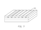
- step 7 referring to FIGS. 15 to 17 , the first PCB substrate 200 and the second PCB substrate 300 are cut along the first imaginary boundary 203 and the second imaginary boundary 303 respectively. Because the filling mass 500 is made of a non-glutinous material and the first portion 420 , the second portion 430 of the adhesive layer 400 is separated form each other, the first unwanted portion 202 and the second unwanted portion 302 can be easily removed after the present step. As such, referring to FIG. 17 , a printed circuit board 800 having a mounting area 801 in a surface of the first main portion 201 exposed from the second main portion 301 is obtained.
- the mounting area 801 is rectangular, and if the first imaginary boundary 203 is a cylinder surface the mounting area 801 may be in a semi-circular like shape.
- the first PCB substrate 200 and the second PCB substrate 300 can be cut using a mold, a laser, or an etching process.
- the metallic layer 320 in the second PCB substrate 300 is etched using an etchant.
- a through groove 321 is formed and the second insulating layer 310 is exposed from the through groove 321 .
- the second insulating layer 310 may be cut using a laser or an etching process.
- Nd:YAG laser has a relative short wave length and can be used to cut metallic layers and insulating layers.
- CO 2 laser has a relative long wave length and can be used to cut insulating layer. Therefore, the insulating layer 310 can be cut using a Nd:YAG laser or a CO 2 laser.
- the Nd:YAG laser can be used to replace the etching step for cutting the metallic layer 320 .
- an filling mass 500 is used to fill the opening 410 in the adhesive layer 400 .
- the first PCB substrate 200 and the second PCB substrate 300 are supported by the filling mass 500 after the first PCB substrate 200 , the second PCB substrate 300 and the adhesive layer 400 are laminated together.
- the first PCB substrate 200 and the second PCB substrate 300 don't bend at the opening 410 , and a quality of the obtained printed circuit board 800 is improved.
Abstract
Description
Claims (3)
Applications Claiming Priority (3)
| Application Number | Priority Date | Filing Date | Title |
|---|---|---|---|
| CN200810300566.0 | 2008-03-14 | ||
| CN200810300566.0A CN101534613B (en) | 2008-03-14 | 2008-03-14 | Method for manufacturing circuit board with offset structure |
| CN200810300566 | 2008-03-14 |
Publications (2)
| Publication Number | Publication Date |
|---|---|
| US20090229121A1 US20090229121A1 (en) | 2009-09-17 |
| US8112880B2 true US8112880B2 (en) | 2012-02-14 |
Family
ID=41061388
Family Applications (1)
| Application Number | Title | Priority Date | Filing Date |
|---|---|---|---|
| US12/342,205 Expired - Fee Related US8112880B2 (en) | 2008-03-14 | 2008-12-23 | Method for manufacturing multilayer printed circuit boards |
Country Status (2)
| Country | Link |
|---|---|
| US (1) | US8112880B2 (en) |
| CN (1) | CN101534613B (en) |
Cited By (2)
| Publication number | Priority date | Publication date | Assignee | Title |
|---|---|---|---|---|
| US8664656B1 (en) | 2012-10-04 | 2014-03-04 | Apple Inc. | Devices and methods for embedding semiconductors in printed circuit boards |
| US11869708B2 (en) * | 2017-09-20 | 2024-01-09 | Murata Manufacturing Co., Ltd. | Method of manufacturing an inductor component |
Families Citing this family (5)
| Publication number | Priority date | Publication date | Assignee | Title |
|---|---|---|---|---|
| CN102083282B (en) * | 2009-11-27 | 2012-11-21 | 富葵精密组件(深圳)有限公司 | Method for manufacturing printed circuit board (PCB) |
| KR101241070B1 (en) * | 2012-10-05 | 2013-03-11 | 주식회사 에스아이 플렉스 | The printed circuit board manufacturing method |
| WO2015129061A1 (en) * | 2014-02-27 | 2015-09-03 | 京セラ株式会社 | Piezoelectric actuator, and piezoelectric vibration device, portable terminal, acoustic generator, acoustic generation device, and electronic device provided therewith |
| CN110831325B (en) * | 2018-08-10 | 2021-04-20 | 鹏鼎控股(深圳)股份有限公司 | Antenna circuit board and manufacturing method thereof |
| CN113438807A (en) * | 2021-06-30 | 2021-09-24 | 东莞市小精灵教育软件有限公司 | Connecting structure of soft board and hard board and manufacturing method thereof |
Citations (1)
| Publication number | Priority date | Publication date | Assignee | Title |
|---|---|---|---|---|
| US5262594A (en) * | 1990-10-12 | 1993-11-16 | Compaq Computer Corporation | Multilayer rigid-flex printed circuit boards for use in infrared reflow oven and method for assembling same |
Family Cites Families (3)
| Publication number | Priority date | Publication date | Assignee | Title |
|---|---|---|---|---|
| US5542175A (en) * | 1994-12-20 | 1996-08-06 | International Business Machines Corporation | Method of laminating and circuitizing substrates having openings therein |
| JP3427011B2 (en) * | 1999-07-19 | 2003-07-14 | 日本メクトロン株式会社 | Method of manufacturing flexible multilayer circuit board |
| KR100688743B1 (en) * | 2005-03-11 | 2007-03-02 | 삼성전기주식회사 | Manufacturing method of PCB having multilayer embedded passive-chips |
-
2008
- 2008-03-14 CN CN200810300566.0A patent/CN101534613B/en active Active
- 2008-12-23 US US12/342,205 patent/US8112880B2/en not_active Expired - Fee Related
Patent Citations (1)
| Publication number | Priority date | Publication date | Assignee | Title |
|---|---|---|---|---|
| US5262594A (en) * | 1990-10-12 | 1993-11-16 | Compaq Computer Corporation | Multilayer rigid-flex printed circuit boards for use in infrared reflow oven and method for assembling same |
Cited By (3)
| Publication number | Priority date | Publication date | Assignee | Title |
|---|---|---|---|---|
| US8664656B1 (en) | 2012-10-04 | 2014-03-04 | Apple Inc. | Devices and methods for embedding semiconductors in printed circuit boards |
| US8809859B2 (en) | 2012-10-04 | 2014-08-19 | Apple Inc. | Devices and methods for embedding semiconductors in printed circuit boards |
| US11869708B2 (en) * | 2017-09-20 | 2024-01-09 | Murata Manufacturing Co., Ltd. | Method of manufacturing an inductor component |
Also Published As
| Publication number | Publication date |
|---|---|
| CN101534613B (en) | 2012-06-13 |
| CN101534613A (en) | 2009-09-16 |
| US20090229121A1 (en) | 2009-09-17 |
Similar Documents
| Publication | Publication Date | Title |
|---|---|---|
| US8112880B2 (en) | Method for manufacturing multilayer printed circuit boards | |
| US8592687B2 (en) | Signal line and circuit substrate | |
| US8042265B2 (en) | Method for manufacturing multilayer flexible printed circuit board | |
| US7581312B2 (en) | Method for manufacturing multilayer flexible printed circuit board | |
| US20090084583A1 (en) | Multilayer printed wiring board and method for fabrication thereof | |
| US8591692B2 (en) | Method for manufacturing rigid-flexible printed circuit board | |
| US7987586B2 (en) | Method for manufacturing printed circuit board having different thicknesses in different areas | |
| JP5201270B2 (en) | Circuit board and manufacturing method thereof | |
| US7897055B2 (en) | Method for manufacturing multilayer flexible printed circuit board | |
| US9445493B2 (en) | Signal line and manufacturing method therefor | |
| JP4147298B2 (en) | Flex-rigid printed wiring board and method for manufacturing flex-rigid printed wiring board | |
| CN216531943U (en) | Laminated body | |
| US7772501B2 (en) | Flexible printed circuit board | |
| US20090038828A1 (en) | Flexible printed circuit board substrate and flexible printed circuit board fabricated using the same | |
| KR102325407B1 (en) | Printed circuit board and manufacturing method thereof | |
| US7992290B2 (en) | Method of making a flexible printed circuit board | |
| KR101946989B1 (en) | The printed circuit board and the method for manufacturing the same | |
| CN113423172B (en) | Rigid-flexible circuit board and manufacturing method thereof | |
| KR101112478B1 (en) | Flexible printed circuit board having low electrical resistance variation | |
| JP2012227404A (en) | Flexible printed wiring board | |
| US8997343B2 (en) | Method for manufacturing multilayer printed circuit board | |
| KR102088033B1 (en) | Method for manufacturing flexible printed circuit board and flexible printed circuit board manufactured by the method | |
| JP2008311544A (en) | Method for manufacturing compound multilayer printed-wiring board | |
| KR101283164B1 (en) | The printed circuit board and the method for manufacturing the same | |
| KR102561936B1 (en) | Printed circuit board |
Legal Events
| Date | Code | Title | Description |
|---|---|---|---|
| AS | Assignment |
Owner name: FUKUI PRECISION COMPONENT (SHENZHEN) CO., LTD., CH Free format text: ASSIGNMENT OF ASSIGNORS INTEREST;ASSIGNORS:ZHANG, HU-HAI;SU, YING;LIN, CHENG-HSIEN;REEL/FRAME:022020/0987 Effective date: 20081010 Owner name: FOXCONN ADVANCED TECHNOLOGY INC., TAIWAN Free format text: ASSIGNMENT OF ASSIGNORS INTEREST;ASSIGNORS:ZHANG, HU-HAI;SU, YING;LIN, CHENG-HSIEN;REEL/FRAME:022020/0987 Effective date: 20081010 |
|
| AS | Assignment |
Owner name: ZHEN DING TECHNOLOGY CO., LTD., TAIWAN Free format text: CHANGE OF NAME;ASSIGNOR:FOXCONN ADVANCED TECHNOLOGY INC.;REEL/FRAME:026894/0653 Effective date: 20110613 |
|
| ZAAA | Notice of allowance and fees due |
Free format text: ORIGINAL CODE: NOA |
|
| ZAAB | Notice of allowance mailed |
Free format text: ORIGINAL CODE: MN/=. |
|
| STCF | Information on status: patent grant |
Free format text: PATENTED CASE |
|
| FPAY | Fee payment |
Year of fee payment: 4 |
|
| AS | Assignment |
Owner name: GARUDA TECHNOLOGY CO., LTD, TAIWAN Free format text: ASSIGNMENT OF ASSIGNORS INTEREST;ASSIGNORS:FUKUI PRECISION COMPONENT (SHENZHEN) CO., LTD.;ZHEN DING TECHNOLOGY CO., LTD.;REEL/FRAME:040979/0066 Effective date: 20170101 Owner name: FUKUI PRECISION COMPONENT (SHENZHEN) CO., LTD., CH Free format text: ASSIGNMENT OF ASSIGNORS INTEREST;ASSIGNORS:FUKUI PRECISION COMPONENT (SHENZHEN) CO., LTD.;ZHEN DING TECHNOLOGY CO., LTD.;REEL/FRAME:040979/0066 Effective date: 20170101 |
|
| AS | Assignment |
Owner name: AVARY HOLDING (SHENZHEN) CO., LIMITED., CHINA Free format text: CHANGE OF NAME;ASSIGNOR:FUKUI PRECISION COMPONENT (SHENZHEN) CO., LTD.;REEL/FRAME:043312/0584 Effective date: 20170524 |
|
| AS | Assignment |
Owner name: AVARY HOLDING (SHENZHEN) CO., LIMITED., CHINA Free format text: CHANGE OF NAME;ASSIGNOR:FUKUI PRECISION COMPONENT (SHENZHEN) CO., LTD.;REEL/FRAME:043378/0038 Effective date: 20170524 |
|
| MAFP | Maintenance fee payment |
Free format text: PAYMENT OF MAINTENANCE FEE, 8TH YEAR, LARGE ENTITY (ORIGINAL EVENT CODE: M1552); ENTITY STATUS OF PATENT OWNER: LARGE ENTITY Year of fee payment: 8 |
|
| FEPP | Fee payment procedure |
Free format text: MAINTENANCE FEE REMINDER MAILED (ORIGINAL EVENT CODE: REM.); ENTITY STATUS OF PATENT OWNER: LARGE ENTITY |
|
| LAPS | Lapse for failure to pay maintenance fees |
Free format text: PATENT EXPIRED FOR FAILURE TO PAY MAINTENANCE FEES (ORIGINAL EVENT CODE: EXP.); ENTITY STATUS OF PATENT OWNER: LARGE ENTITY |
|
| STCH | Information on status: patent discontinuation |
Free format text: PATENT EXPIRED DUE TO NONPAYMENT OF MAINTENANCE FEES UNDER 37 CFR 1.362 |
|
| FP | Lapsed due to failure to pay maintenance fee |
Effective date: 20240214 |