US7581312B2 - Method for manufacturing multilayer flexible printed circuit board - Google Patents
Method for manufacturing multilayer flexible printed circuit board Download PDFInfo
- Publication number
- US7581312B2 US7581312B2 US11/877,585 US87758507A US7581312B2 US 7581312 B2 US7581312 B2 US 7581312B2 US 87758507 A US87758507 A US 87758507A US 7581312 B2 US7581312 B2 US 7581312B2
- Authority
- US
- United States
- Prior art keywords
- copper clad
- clad laminate
- binder layer
- defining
- excess portion
- Prior art date
- Legal status (The legal status is an assumption and is not a legal conclusion. Google has not performed a legal analysis and makes no representation as to the accuracy of the status listed.)
- Active
Links
Images


Classifications
-
- H—ELECTRICITY
- H05—ELECTRIC TECHNIQUES NOT OTHERWISE PROVIDED FOR
- H05K—PRINTED CIRCUITS; CASINGS OR CONSTRUCTIONAL DETAILS OF ELECTRIC APPARATUS; MANUFACTURE OF ASSEMBLAGES OF ELECTRICAL COMPONENTS
- H05K3/00—Apparatus or processes for manufacturing printed circuits
- H05K3/46—Manufacturing multilayer circuits
- H05K3/4697—Manufacturing multilayer circuits having cavities, e.g. for mounting components
-
- H—ELECTRICITY
- H05—ELECTRIC TECHNIQUES NOT OTHERWISE PROVIDED FOR
- H05K—PRINTED CIRCUITS; CASINGS OR CONSTRUCTIONAL DETAILS OF ELECTRIC APPARATUS; MANUFACTURE OF ASSEMBLAGES OF ELECTRICAL COMPONENTS
- H05K3/00—Apparatus or processes for manufacturing printed circuits
- H05K3/46—Manufacturing multilayer circuits
- H05K3/4611—Manufacturing multilayer circuits by laminating two or more circuit boards
- H05K3/4626—Manufacturing multilayer circuits by laminating two or more circuit boards characterised by the insulating layers or materials
- H05K3/4635—Manufacturing multilayer circuits by laminating two or more circuit boards characterised by the insulating layers or materials laminating flexible circuit boards using additional insulating adhesive materials between the boards
-
- H—ELECTRICITY
- H05—ELECTRIC TECHNIQUES NOT OTHERWISE PROVIDED FOR
- H05K—PRINTED CIRCUITS; CASINGS OR CONSTRUCTIONAL DETAILS OF ELECTRIC APPARATUS; MANUFACTURE OF ASSEMBLAGES OF ELECTRICAL COMPONENTS
- H05K1/00—Printed circuits
- H05K1/02—Details
- H05K1/03—Use of materials for the substrate
- H05K1/0393—Flexible materials
-
- H—ELECTRICITY
- H05—ELECTRIC TECHNIQUES NOT OTHERWISE PROVIDED FOR
- H05K—PRINTED CIRCUITS; CASINGS OR CONSTRUCTIONAL DETAILS OF ELECTRIC APPARATUS; MANUFACTURE OF ASSEMBLAGES OF ELECTRICAL COMPONENTS
- H05K2201/00—Indexing scheme relating to printed circuits covered by H05K1/00
- H05K2201/09—Shape and layout
- H05K2201/09009—Substrate related
- H05K2201/0909—Preformed cutting or breaking line
-
- H—ELECTRICITY
- H05—ELECTRIC TECHNIQUES NOT OTHERWISE PROVIDED FOR
- H05K—PRINTED CIRCUITS; CASINGS OR CONSTRUCTIONAL DETAILS OF ELECTRIC APPARATUS; MANUFACTURE OF ASSEMBLAGES OF ELECTRICAL COMPONENTS
- H05K2201/00—Indexing scheme relating to printed circuits covered by H05K1/00
- H05K2201/09—Shape and layout
- H05K2201/09009—Substrate related
- H05K2201/09127—PCB or component having an integral separable or breakable part
-
- H—ELECTRICITY
- H05—ELECTRIC TECHNIQUES NOT OTHERWISE PROVIDED FOR
- H05K—PRINTED CIRCUITS; CASINGS OR CONSTRUCTIONAL DETAILS OF ELECTRIC APPARATUS; MANUFACTURE OF ASSEMBLAGES OF ELECTRICAL COMPONENTS
- H05K2203/00—Indexing scheme relating to apparatus or processes for manufacturing printed circuits covered by H05K3/00
- H05K2203/06—Lamination
- H05K2203/063—Lamination of preperforated insulating layer
-
- H—ELECTRICITY
- H05—ELECTRIC TECHNIQUES NOT OTHERWISE PROVIDED FOR
- H05K—PRINTED CIRCUITS; CASINGS OR CONSTRUCTIONAL DETAILS OF ELECTRIC APPARATUS; MANUFACTURE OF ASSEMBLAGES OF ELECTRICAL COMPONENTS
- H05K3/00—Apparatus or processes for manufacturing printed circuits
- H05K3/46—Manufacturing multilayer circuits
- H05K3/4611—Manufacturing multilayer circuits by laminating two or more circuit boards
-
- Y—GENERAL TAGGING OF NEW TECHNOLOGICAL DEVELOPMENTS; GENERAL TAGGING OF CROSS-SECTIONAL TECHNOLOGIES SPANNING OVER SEVERAL SECTIONS OF THE IPC; TECHNICAL SUBJECTS COVERED BY FORMER USPC CROSS-REFERENCE ART COLLECTIONS [XRACs] AND DIGESTS
- Y10—TECHNICAL SUBJECTS COVERED BY FORMER USPC
- Y10T—TECHNICAL SUBJECTS COVERED BY FORMER US CLASSIFICATION
- Y10T29/00—Metal working
- Y10T29/49—Method of mechanical manufacture
- Y10T29/49002—Electrical device making
- Y10T29/49117—Conductor or circuit manufacturing
- Y10T29/49124—On flat or curved insulated base, e.g., printed circuit, etc.
- Y10T29/49126—Assembling bases
-
- Y—GENERAL TAGGING OF NEW TECHNOLOGICAL DEVELOPMENTS; GENERAL TAGGING OF CROSS-SECTIONAL TECHNOLOGIES SPANNING OVER SEVERAL SECTIONS OF THE IPC; TECHNICAL SUBJECTS COVERED BY FORMER USPC CROSS-REFERENCE ART COLLECTIONS [XRACs] AND DIGESTS
- Y10—TECHNICAL SUBJECTS COVERED BY FORMER USPC
- Y10T—TECHNICAL SUBJECTS COVERED BY FORMER US CLASSIFICATION
- Y10T29/00—Metal working
- Y10T29/49—Method of mechanical manufacture
- Y10T29/49002—Electrical device making
- Y10T29/49117—Conductor or circuit manufacturing
- Y10T29/49124—On flat or curved insulated base, e.g., printed circuit, etc.
- Y10T29/49128—Assembling formed circuit to base
-
- Y—GENERAL TAGGING OF NEW TECHNOLOGICAL DEVELOPMENTS; GENERAL TAGGING OF CROSS-SECTIONAL TECHNOLOGIES SPANNING OVER SEVERAL SECTIONS OF THE IPC; TECHNICAL SUBJECTS COVERED BY FORMER USPC CROSS-REFERENCE ART COLLECTIONS [XRACs] AND DIGESTS
- Y10—TECHNICAL SUBJECTS COVERED BY FORMER USPC
- Y10T—TECHNICAL SUBJECTS COVERED BY FORMER US CLASSIFICATION
- Y10T29/00—Metal working
- Y10T29/49—Method of mechanical manufacture
- Y10T29/49002—Electrical device making
- Y10T29/49117—Conductor or circuit manufacturing
- Y10T29/49124—On flat or curved insulated base, e.g., printed circuit, etc.
- Y10T29/4913—Assembling to base an electrical component, e.g., capacitor, etc.
- Y10T29/49139—Assembling to base an electrical component, e.g., capacitor, etc. by inserting component lead or terminal into base aperture
-
- Y—GENERAL TAGGING OF NEW TECHNOLOGICAL DEVELOPMENTS; GENERAL TAGGING OF CROSS-SECTIONAL TECHNOLOGIES SPANNING OVER SEVERAL SECTIONS OF THE IPC; TECHNICAL SUBJECTS COVERED BY FORMER USPC CROSS-REFERENCE ART COLLECTIONS [XRACs] AND DIGESTS
- Y10—TECHNICAL SUBJECTS COVERED BY FORMER USPC
- Y10T—TECHNICAL SUBJECTS COVERED BY FORMER US CLASSIFICATION
- Y10T29/00—Metal working
- Y10T29/49—Method of mechanical manufacture
- Y10T29/49002—Electrical device making
- Y10T29/49117—Conductor or circuit manufacturing
- Y10T29/49124—On flat or curved insulated base, e.g., printed circuit, etc.
- Y10T29/4913—Assembling to base an electrical component, e.g., capacitor, etc.
- Y10T29/49146—Assembling to base an electrical component, e.g., capacitor, etc. with encapsulating, e.g., potting, etc.
-
- Y—GENERAL TAGGING OF NEW TECHNOLOGICAL DEVELOPMENTS; GENERAL TAGGING OF CROSS-SECTIONAL TECHNOLOGIES SPANNING OVER SEVERAL SECTIONS OF THE IPC; TECHNICAL SUBJECTS COVERED BY FORMER USPC CROSS-REFERENCE ART COLLECTIONS [XRACs] AND DIGESTS
- Y10—TECHNICAL SUBJECTS COVERED BY FORMER USPC
- Y10T—TECHNICAL SUBJECTS COVERED BY FORMER US CLASSIFICATION
- Y10T29/00—Metal working
- Y10T29/49—Method of mechanical manufacture
- Y10T29/49002—Electrical device making
- Y10T29/49117—Conductor or circuit manufacturing
- Y10T29/49124—On flat or curved insulated base, e.g., printed circuit, etc.
- Y10T29/49155—Manufacturing circuit on or in base
- Y10T29/49165—Manufacturing circuit on or in base by forming conductive walled aperture in base
Definitions
- the present invention relates to a method for manufacturing a flexible printed circuit board, and especially to a method for manufacturing a multilayer flexible printed circuit board having different number of layers in different areas.
- FPCBs Flexible printed circuit boards
- electronic products such as mobile phones, printing heads and hard disks.
- FPCBs can assure power supply and signal transmission in such environment due to their excellent flexibility.
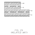
- FIG. 30 shows a multilayer FPCB structure, which has different numbers of layers in different areas; in other words, there are thick areas and thin areas within the same FPCB.
- the thick area can have a higher circuit density whilst the thin area exhibits higher flexibility.
- FIGS. 25-30 show a process for manufacturing such a type of FPCB.
- a first copper clad laminate (CCL) 41 a binder layer 45 and a second CCL 42 are laminated.
- dry films 412 , 422 are applied on the first CCL 41 and the second CCL 42 respectively and then the dry films 412 , 422 are exposed and developed. Because there is a cliff-like thickness difference between the first CCL 41 and the second CCL 42 , a gap 46 is formed at ‘cliff’.
- the etchant can seep into the gap 46 and react with dielectric layers in the first CCL 41 and the second CCL 42 . As a result the dielectric layers may peel from the CCL.
- a third CCL 43 and a fourth CCL 44 are laminated with the first CCL 41 and the second CCL 42 .
- a via hole 47 is formed.
- the via hole 47 can be made by drilling or by laser ablation.
- a conductive layer is formed on a surface of the via hole 47 by electroless plating or electroplating.
- the dielectric layer of the second CCL 42 is exposed to a plating solution, thereby forming a number of copper lumps thereon. These copper lumps can pierce dry film that is applied onto the second CCL 42 in the next pattern-forming process, and etchant used for developing the dry film can react with dielectric layer or copper layer of second CCL 42 and cause poor quality products to be formed.
- a method for manufacturing a multilayer FPCB includes the steps of: firstly, providing a first copper clad laminate, a second copper clad laminate and a binder layer.
- the first copper clad laminate and the second copper clad laminate each including at least one single-sided copper clad laminate, the single-sided copper clad laminate includes a dielectric layer and a conductive layer formed on the dielectric layer.
- the first copper clad laminate having an excess portion.
- defining an opening in the binder layer Thirdly, defining a first slit in the first copper clad laminate along a boundary of the excess portion of the first copper clad laminate.
- FIG. 1 is a flow chart shows a method for manufacturing a multilayer FPCB having different number of layers in different areas
- FIGS. 2 to 12 are schematic views show a process for manufacturing a multilayer FPCB having different number of layers in different areas in accordance with first preferred embodiment
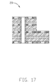
- FIGS. 13 to 17 are schematic views show a process for manufacturing a multilayer FPCB having different number of layers in different areas in accordance with the second preferred embodiment
- FIGS. 18 to 24 are schematic views show a process for manufacturing a multilayer FPCB having different number of layers in different areas in accordance with the third preferred embodiment.
- FIGS. 25 to 30 are schematic views show a process in related art for manufacturing a multilayer FPCB having different number of layers in different areas in accordance with related art.
- a method for manufacturing a multilayer FPCB having different number of layers in different areas includes the steps in no particular order of:
- FIGS. 2-12 show a process for manufacturing a FPCB that has different number of layers in different areas in accordance with a first preferred embodiment.
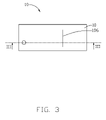
- a first copper clad laminate 10 includes two single-sided copper clad laminates 11 and 12 .
- the single-sided copper clad laminate 11 includes a dielectric layer 112 and a conductive layer 111 formed on the dielectric layer 112 .
- the single-sided copper clad laminate 12 includes a dielectric layer 122 and a conductive layer 121 formed on the dielectric layer 122 .
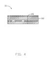
- the single-sided copper clad laminates 11 and 12 are conglutinated by binder layer 15 .
- the second copper clad laminate 13 has a similar structure with the first copper clad laminate 10 .
- the binder layer 16 is used for conglutinating the first copper clad laminate 10 and the second copper clad laminate 13 .
- a locating hole 104 can be formed in the first copper clad laminate 11 , the binder layer and the second copper clad laminate.
- Materials of the dielectric layers and the binder layers can be selected from the group consisting of polyimide, polytetrafluoroethylene, polythiamine, polymethacrylic acid, polycarbonate, polycarbonate ester, polyester, and copolymer of imide, ethylene and dimethyl terephthate.
- the conductive layers can be a film of copper, silver or aluminum.
- the first copper clad laminate 10 includes an excess portion 102 (i.e. a sacrificing portion which will be removed in a later step), a first slit 106 is formed along a boundary of the excess portion 102 .
- a length of the first slit 106 is less than a width of the first copper clad laminate 10 .
- the first slit 106 can be formed by stamping or laser ablation. In this preferred embodiment, the first slit 106 is formed by stamping.
- an opening 162 is formed in the binder layer 16 thereby an inner side wall surface 164 of the binder layer 16 is formed.
- the opening 162 can be formed by cutting, stamping, laser ablation or etching.
- the opening 162 has a rectangular shape, but the opening 162 can also be of other shape, for example, trapezium, triangle etc.
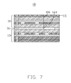
- the first copper clad laminate 10 , the binder layer 16 and the second copper clad laminate 13 are laminated.
- the first slit 106 is aligned with the inner side wall surface 164 . If there are locating holes on the first copper clad laminate, the binder layer 16 , aligning with the first slit 106 and the inner side wall surface 164 can be achieved using the locating holes.
- the first slit 106 can also be separated from the inner side wall surface 164 1 to 2 millimeters in the direction away from the opening 162 , in this manner, the first slit 106 is not directly in communication with the opening 162 , therefore liquid such as etchant cannot seep through the first slit 106 into the opening 162 . In other words, a majority of the excess portion 102 of the first copper clad laminate 10 is exposed to and suspended above the opening 162 of the binder layer 16 .
- a via hole 17 is formed.
- the via hole 17 establishes an electrical connection between the first copper clad laminate 10 and the second copper clad laminate 13 .
- conductive patterns are formed in outer surfaces of the first copper clad laminate 10 and the second copper clad laminate 13 , in other words, conductive patterns are formed in conductive layers 111 and 141 .
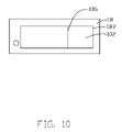
- the first copper clad laminate 10 , the binder layer 16 and the second copper clad laminate 13 are cut thereby forming a second slit 182 .
- the second slit 182 defines a profile of a FPCB.
- the second slit 182 and the first slit 106 surround the excess portion 102 of the first copper clad laminate 10 .
- the excess portion 102 is not conglutinated by the binder layer 16 and is therefore very easy to remove.
- the portion 102 is removed thereby a multilayer FPCB 14 having different number of layers in different areas is obtained.
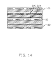
- the method for manufacturing a multilayer FPCB having different numbers of layers in different areas in accordance with the second preferred embodiment is similar to that of the first preferred embodiment, referring to FIG. 13 .
- the conductive patterns on outer surfaces of the first copper clad laminate 20 and the second copper clad laminate 23 are formed before the first copper clad laminate 20 and the second copper clad laminate 23 are laminated.
- the first copper clad laminate 20 and the second copper clad laminate 23 are laminated, and the first copper clad laminate 20 and the second copper clad laminate 23 are conglutinated by the binder layer 25 .
- the first slit 206 is aligned with the side 254 .
- protecting films 231 and 232 are applied on the conductive layers 211 and 241 respectively.
- the protecting films 231 and 232 are used for protecting the conductive layers 211 and 241 from being attacked by an etchant used in the next process.
- a via hole 27 is formed. After the via hole 27 is formed the protecting films 27 are removed.
- the first copper clad laminate 20 , the binder layer 25 and the second copper clad laminate 23 are cut in a manner similar to that in the first preferred embodiment and therefore a multilayer FPCB 24 having different numbers of layers in different areas is obtained.
- FIGS. 18 to 24 show a process for manufacturing a multilayer FPCB having different number of layers in different areas in accordance with third preferred embodiment.
- the first single-sided copper clad laminate 31 includes a dielectric layer 311 and a conductive layer 312 formed on the dielectric layer 311 , a slit 316 is preformed on the first copper clad laminate 31 .
- the second single-sided copper clad laminate 32 includes a dielectric layer 321 and a conductive layer 322 formed on the dielectric layer 321 .
- the binder layer 35 includes a preformed opening 352 and a side 354 corresponding to the opening 352 .
- the first single-sided copper clad laminate 31 , the binder layer 35 and the second single-sided copper clad laminate 32 are laminated.
- the slit 316 is aligned with the side 354 .
- conductive patterns are formed on the first single-sided copper clad laminate 31 and the second single-sided copper clad laminate 32 .
- the slit 336 is aligned with the slit 316 .
- a first single-sided copper clad laminate 33 and a second single-sided copper clad laminate 34 are applied on and then laminated with the first single-sided copper clad laminate 31 and the second single-sided copper clad laminate 32 respectively.
- the binder layer 36 conglutinates the first single-sided copper clad laminate 31 and 33 .
- the binder layer 37 conglutinates the second single-sided copper clad laminate 32 and 34 .
- the first single-sided copper clad laminate 33 has a similar structure to the first copper clad laminate 31 .
- a slit 336 is preformed on the first single-sided copper clad laminate 33 .
- a slit 362 is preformed on the binder layer 36 .
- the slit 316 , 336 and 362 are aligned with the side 354 thereby constitute a slit 306 .
- a via hole 38 is formed.
- the via hole 38 is used for conducting the first copper clad laminate 31 , 33 and the second copper clad laminate 32 , 34 .
- conductive patterns are formed on outer surfaces of the first copper clad laminate 33 and the second copper clad laminate 34 .
- the first copper clad laminates 31 and 33 , the second copper clad laminates 32 and 34 , and binder layers 35 , 36 and 37 are cut in manner similar to that of the first preferred embodiment, therefore a multilayer FPCB having different number of layers in different areas is obtained.
Landscapes
- Engineering & Computer Science (AREA)
- Manufacturing & Machinery (AREA)
- Microelectronics & Electronic Packaging (AREA)
- Production Of Multi-Layered Print Wiring Board (AREA)
Abstract
Description
- defining an opening in the binder layer;
- defining a first slit in the first copper clad laminate;
- laminating the first copper clad laminate and the second copper clad laminate on opposite sides of the binder layer;
- forming a via hole for establishing an electric connection between the first copper clad laminate and the second copper clad laminate; and
- defining a second slit in the first copper clad laminate.
Claims (13)
Applications Claiming Priority (2)
| Application Number | Priority Date | Filing Date | Title |
|---|---|---|---|
| CN200610157702.6A CN101207977B (en) | 2006-12-20 | 2006-12-20 | Method for making flexible circuit board with break difference structure |
| CN200610157702.6 | 2006-12-20 |
Publications (2)
| Publication Number | Publication Date |
|---|---|
| US20080148562A1 US20080148562A1 (en) | 2008-06-26 |
| US7581312B2 true US7581312B2 (en) | 2009-09-01 |
Family
ID=39540849
Family Applications (1)
| Application Number | Title | Priority Date | Filing Date |
|---|---|---|---|
| US11/877,585 Active US7581312B2 (en) | 2006-12-20 | 2007-10-23 | Method for manufacturing multilayer flexible printed circuit board |
Country Status (2)
| Country | Link |
|---|---|
| US (1) | US7581312B2 (en) |
| CN (1) | CN101207977B (en) |
Cited By (2)
| Publication number | Priority date | Publication date | Assignee | Title |
|---|---|---|---|---|
| US20080116166A1 (en) * | 2006-11-17 | 2008-05-22 | Foxconn Advanced Technology Inc. | Method for manufacturing multilayer flexible printed circuit board |
| US20120247811A1 (en) * | 2011-04-01 | 2012-10-04 | Advanced Flexible Circuits Co., Ltd. | Composite circuit board with fracturable structure |
Families Citing this family (14)
| Publication number | Priority date | Publication date | Assignee | Title |
|---|---|---|---|---|
| TW201130405A (en) * | 2010-02-23 | 2011-09-01 | Ibiden Co Ltd | Flex-rigid wiring board and method for manufacturing the same |
| CN102340938B (en) * | 2010-07-29 | 2013-08-28 | 富葵精密组件(深圳)有限公司 | Circuit board manufacturing method |
| CN102223752B (en) * | 2011-06-02 | 2013-07-24 | 宝利时(深圳)胶粘制品有限公司 | Multi-layer flexible circuit board and manufacturing method thereof |
| KR102497358B1 (en) * | 2015-09-24 | 2023-02-10 | 주식회사 기가레인 | Flexible printed circuit board having improved bending durabiliy |
| CN105578778A (en) * | 2015-12-17 | 2016-05-11 | 江门崇达电路技术有限公司 | Manufacturing method of single-face local thick-gold plated PCB |
| CN105682380B (en) * | 2016-02-03 | 2018-11-06 | 江门崇达电路技术有限公司 | A kind of production method of the thick gold PCB of parcel plating |
| CN108112178A (en) * | 2017-12-25 | 2018-06-01 | 广州兴森快捷电路科技有限公司 | Circuit board fabrication method |
| KR102154193B1 (en) * | 2018-02-20 | 2020-09-09 | 주식회사 아모그린텍 | Flexible printed circuit board |
| CN110831325B (en) * | 2018-08-10 | 2021-04-20 | 鹏鼎控股(深圳)股份有限公司 | Antenna circuit board and manufacturing method thereof |
| CN112216819B (en) * | 2019-07-10 | 2021-10-15 | 上海展枭新能源科技有限公司 | Large-scale production method of copper-lithium composite electrode |
| CN113498249B (en) * | 2020-04-07 | 2023-11-10 | 庆鼎精密电子(淮安)有限公司 | Soft-hard combined circuit board and preparation method thereof |
| CN112638045A (en) * | 2021-03-09 | 2021-04-09 | 福莱盈电子股份有限公司 | Method for processing through hole and blind hole of multilayer flexible board |
| CN114302565B (en) * | 2022-01-05 | 2024-08-30 | 安捷利电子科技(苏州)有限公司 | FPC with steps and preparation method thereof |
| CN115460804A (en) * | 2022-10-12 | 2022-12-09 | 江西弘信柔性电子科技有限公司 | Processing method of ultrathin four-layer flexible board |
Citations (1)
| Publication number | Priority date | Publication date | Assignee | Title |
|---|---|---|---|---|
| US6687984B1 (en) * | 1999-07-19 | 2004-02-10 | Nippon Mektron, Ltd. | Method for manufacturing flexible multilayer circuit board |
Family Cites Families (2)
| Publication number | Priority date | Publication date | Assignee | Title |
|---|---|---|---|---|
| US5542175A (en) * | 1994-12-20 | 1996-08-06 | International Business Machines Corporation | Method of laminating and circuitizing substrates having openings therein |
| JP4401912B2 (en) * | 2003-10-17 | 2010-01-20 | 学校法人早稲田大学 | Method for forming semiconductor multilayer wiring board |
-
2006
- 2006-12-20 CN CN200610157702.6A patent/CN101207977B/en not_active Expired - Fee Related
-
2007
- 2007-10-23 US US11/877,585 patent/US7581312B2/en active Active
Patent Citations (1)
| Publication number | Priority date | Publication date | Assignee | Title |
|---|---|---|---|---|
| US6687984B1 (en) * | 1999-07-19 | 2004-02-10 | Nippon Mektron, Ltd. | Method for manufacturing flexible multilayer circuit board |
Cited By (3)
| Publication number | Priority date | Publication date | Assignee | Title |
|---|---|---|---|---|
| US20080116166A1 (en) * | 2006-11-17 | 2008-05-22 | Foxconn Advanced Technology Inc. | Method for manufacturing multilayer flexible printed circuit board |
| US7897055B2 (en) * | 2006-11-17 | 2011-03-01 | Foxconn Advanced Technology Inc. | Method for manufacturing multilayer flexible printed circuit board |
| US20120247811A1 (en) * | 2011-04-01 | 2012-10-04 | Advanced Flexible Circuits Co., Ltd. | Composite circuit board with fracturable structure |
Also Published As
| Publication number | Publication date |
|---|---|
| CN101207977A (en) | 2008-06-25 |
| US20080148562A1 (en) | 2008-06-26 |
| CN101207977B (en) | 2012-03-21 |
Similar Documents
| Publication | Publication Date | Title |
|---|---|---|
| US7581312B2 (en) | Method for manufacturing multilayer flexible printed circuit board | |
| US8042265B2 (en) | Method for manufacturing multilayer flexible printed circuit board | |
| US7897055B2 (en) | Method for manufacturing multilayer flexible printed circuit board | |
| US7987586B2 (en) | Method for manufacturing printed circuit board having different thicknesses in different areas | |
| JP5198105B2 (en) | Manufacturing method of multilayer flexible printed wiring board | |
| US8181339B2 (en) | Method of manufacturing a printed circuit board | |
| CN112333926B (en) | Method for manufacturing circuit board with metal layers with different thicknesses | |
| US10064292B2 (en) | Recessed cavity in printed circuit board protected by LPI | |
| CN102387672A (en) | Method for manufacturing multilayer circuit board | |
| US8112880B2 (en) | Method for manufacturing multilayer printed circuit boards | |
| TWI778356B (en) | Rigid-flexible circuit board and method of manufacturing the same | |
| KR101987378B1 (en) | Method of manufacturing printed circuit board | |
| US7992290B2 (en) | Method of making a flexible printed circuit board | |
| US7772501B2 (en) | Flexible printed circuit board | |
| CN115460772A (en) | Printed circuit board, printed circuit board preparation method and electronic equipment | |
| CN113973420A (en) | Rigid-flex board and manufacturing method thereof | |
| KR100632564B1 (en) | Flexible Printed Circuit Board and Manufacturing Method Thereof | |
| EP1523231A1 (en) | Method of producing multilayer wired circuit board | |
| CN113133202B (en) | Embedded capacitor circuit board and manufacturing method thereof | |
| KR20070076590A (en) | Manufacturing method of rigid flexible printed circuit board | |
| JPH0818228A (en) | Manufacture of multi-layer printed board | |
| KR100588770B1 (en) | Double-sided flexible circuit board and manufacturing method | |
| JP4302045B2 (en) | Multilayer flexible circuit wiring board and manufacturing method thereof | |
| TW201134336A (en) | Flexible printed circuit board and manufacturing method thereof | |
| KR102119604B1 (en) | Flexible printed circuit board and manufacturing method of the same |
Legal Events
| Date | Code | Title | Description |
|---|---|---|---|
| AS | Assignment |
Owner name: FOXCONN ADVANCED TECHNOLOGY INC., TAIWAN Free format text: ASSIGNMENT OF ASSIGNORS INTEREST;ASSIGNORS:TU, CHIH-YI;LIN, CHENG-HSIEN;WANG, MING;REEL/FRAME:020003/0475 Effective date: 20071018 Owner name: FUKUI PRECISION COMPONENT (SHENZHEN) CO., LTD., CH Free format text: ASSIGNMENT OF ASSIGNORS INTEREST;ASSIGNORS:TU, CHIH-YI;LIN, CHENG-HSIEN;WANG, MING;REEL/FRAME:020003/0475 Effective date: 20071018 |
|
| STCF | Information on status: patent grant |
Free format text: PATENTED CASE |
|
| AS | Assignment |
Owner name: ZHEN DING TECHNOLOGY CO., LTD., TAIWAN Free format text: CHANGE OF NAME;ASSIGNOR:FOXCONN ADVANCED TECHNOLOGY INC.;REEL/FRAME:026893/0919 Effective date: 20110613 |
|
| FPAY | Fee payment |
Year of fee payment: 4 |
|
| AS | Assignment |
Owner name: FUKUI PRECISION COMPONENT (SHENZHEN) CO., LTD., CH Free format text: ASSIGNMENT OF ASSIGNORS INTEREST;ASSIGNORS:FUKUI PRECISION COMPONENT (SHENZHEN) CO., LTD.;ZHEN DING TECHNOLOGY CO., LTD.;REEL/FRAME:040978/0636 Effective date: 20170101 Owner name: GARUDA TECHNOLOGY CO., LTD, TAIWAN Free format text: ASSIGNMENT OF ASSIGNORS INTEREST;ASSIGNORS:FUKUI PRECISION COMPONENT (SHENZHEN) CO., LTD.;ZHEN DING TECHNOLOGY CO., LTD.;REEL/FRAME:040978/0636 Effective date: 20170101 |
|
| FPAY | Fee payment |
Year of fee payment: 8 |
|
| AS | Assignment |
Owner name: AVARY HOLDING (SHENZHEN) CO., LIMITED., CHINA Free format text: CHANGE OF NAME;ASSIGNOR:FUKUI PRECISION COMPONENT (SHENZHEN) CO., LTD.;REEL/FRAME:043312/0490 Effective date: 20170524 |
|
| AS | Assignment |
Owner name: AVARY HOLDING (SHENZHEN) CO., LIMITED., CHINA Free format text: CHANGE OF NAME;ASSIGNOR:FUKUI PRECISION COMPONENT (SHENZHEN) CO., LTD.;REEL/FRAME:043378/0038 Effective date: 20170524 |
|
| MAFP | Maintenance fee payment |
Free format text: PAYMENT OF MAINTENANCE FEE, 12TH YEAR, LARGE ENTITY (ORIGINAL EVENT CODE: M1553); ENTITY STATUS OF PATENT OWNER: LARGE ENTITY Year of fee payment: 12 |