US8089155B2 - High performance system-on-chip discrete components using post passivation process - Google Patents
High performance system-on-chip discrete components using post passivation process Download PDFInfo
- Publication number
- US8089155B2 US8089155B2 US11/062,276 US6227605A US8089155B2 US 8089155 B2 US8089155 B2 US 8089155B2 US 6227605 A US6227605 A US 6227605A US 8089155 B2 US8089155 B2 US 8089155B2
- Authority
- US
- United States
- Prior art keywords
- layer
- over
- contact point
- passive device
- integrated circuit
- Prior art date
- Legal status (The legal status is an assumption and is not a legal conclusion. Google has not performed a legal analysis and makes no representation as to the accuracy of the status listed.)
- Expired - Fee Related, expires
Links
Images


Classifications
-
- H10W20/40—
-
- H—ELECTRICITY
- H10—SEMICONDUCTOR DEVICES; ELECTRIC SOLID-STATE DEVICES NOT OTHERWISE PROVIDED FOR
- H10D—INORGANIC ELECTRIC SEMICONDUCTOR DEVICES
- H10D1/00—Resistors, capacitors or inductors
- H10D1/20—Inductors
-
- H—ELECTRICITY
- H10—SEMICONDUCTOR DEVICES; ELECTRIC SOLID-STATE DEVICES NOT OTHERWISE PROVIDED FOR
- H10D—INORGANIC ELECTRIC SEMICONDUCTOR DEVICES
- H10D1/00—Resistors, capacitors or inductors
- H10D1/40—Resistors
- H10D1/47—Resistors having no potential barriers
-
- H—ELECTRICITY
- H10—SEMICONDUCTOR DEVICES; ELECTRIC SOLID-STATE DEVICES NOT OTHERWISE PROVIDED FOR
- H10D—INORGANIC ELECTRIC SEMICONDUCTOR DEVICES
- H10D84/00—Integrated devices formed in or on semiconductor substrates that comprise only semiconducting layers, e.g. on Si wafers or on GaAs-on-Si wafers
- H10D84/201—Integrated devices formed in or on semiconductor substrates that comprise only semiconducting layers, e.g. on Si wafers or on GaAs-on-Si wafers characterised by the integration of only components covered by H10D1/00 or H10D8/00, e.g. RLC circuits
- H10D84/204—Integrated devices formed in or on semiconductor substrates that comprise only semiconducting layers, e.g. on Si wafers or on GaAs-on-Si wafers characterised by the integration of only components covered by H10D1/00 or H10D8/00, e.g. RLC circuits of combinations of diodes or capacitors or resistors
-
- H10W20/427—
-
- H10W20/48—
-
- H10W20/495—
-
- H10W20/496—
-
- H10W20/497—
-
- H10W20/498—
-
- H10W42/60—
-
- H10W44/401—
-
- H10W44/501—
-
- H10W44/601—
-
- H10W72/012—
-
- H10W72/019—
-
- H10W70/05—
-
- H10W70/655—
-
- H10W72/01223—
-
- H10W72/01225—
-
- H10W72/01235—
-
- H10W72/01257—
-
- H10W72/01935—
-
- H10W72/01938—
-
- H10W72/01953—
-
- H10W72/01955—
-
- H10W72/072—
-
- H10W72/241—
-
- H10W72/242—
-
- H10W72/252—
-
- H10W72/29—
-
- H10W72/352—
-
- H10W72/354—
-
- H10W72/5522—
-
- H10W72/5524—
-
- H10W72/59—
-
- H10W72/90—
-
- H10W72/922—
-
- H10W72/923—
-
- H10W74/147—
-
- H10W90/728—
Definitions
- the invention relates to the manufacturing of high performance Integrated Circuit (IC's), and, more specifically, to methods of creating high performance electrical components (such as an inductor) on the surface of a semiconductor substrate by reducing the electromagnetic losses that are typically incurred in the surface of the substrate.
- IC Integrated Circuit
- RF amplifiers contain a number of standard components, a major component of a typical RF amplifier is a tuned circuit that contains inductive and capacitive components. Tuned circuits form, dependent on and determined by the values of their inductive and capacitive components, an impedance that is frequency dependent, enabling the tuned circuit to either present a high or a low impedance for signals of a certain frequency.
- the tuned circuit can therefore either reject or pass and further amplify components of an analog signal, based on the frequency of that component.
- the tuned circuit can in this manner be used as a filter to filter out or remove signals of certain frequencies or to remove noise from a circuit configuration that is aimed at processing analog signals.
- the tuned circuit can also be used to form a high electrical impedance by using the LC resonance of the circuit and to thereby counteract the effects of parasitic capacitances that are part of a circuit.
- One of the problems that is encountered when creating an inductor on the surface of a semiconductor substrate is that the self-resonance that is caused by the parasitic capacitance between the (spiral) inductor and the underlying substrate will limit the use of the inductor at high frequencies. As part of the design of such an inductor it is therefore of importance to reduce the capacitive coupling between the created inductor and the underlying substrate.
- the electromagnetic field that is generated by the inductor induces eddy currents in the underlying silicon substrate. Since the silicon substrate is a resistive conductor, the eddy currents will consume electromagnetic energy resulting in significant energy loss, resulting in a low Q inductor. This is one of the main reasons for a low Q value of a inductor, whereby the resonant frequency of 1/ ⁇ (LC) limits the upper boundary of the frequency. In addition, the eddy currents that are induced by the inductor will interfere with the performance of circuitry that is in close physical proximity to the inductor. Furthermore, the fine metal lines used to form the inductor also consume energy, due to the metal's resistance, and result in low Q inductors.
- inductor that forms part of an LC resonance circuit.
- the creation of the inductor must incorporate the minimization of the surface area that is required for the inductor, while at the same time maintaining a high Q value for the inductor.
- inductors that are created on the surface of a substrate are of a spiral shape whereby the spiral is created in a plane that is parallel with the plane of the surface of the substrate.
- Conventional methods that are used to create the inductor on the surface of a substrate suffer several limitations.
- MMIC Monolithic Microwave Integrated Circuits
- the spiral form of the inductor that is created on the surface of a semiconductor substrate results, due to the physical size of the inductor, in parasitic capacitances between the inductor wiring and the underlying substrate and causes electromagnetic energy losses in the underlying resistive silicon substrate. These parasitic capacitances have a serious negative effect on the functionality of the created LC circuit by sharply reducing the frequency of resonance of the tuned circuit of the application.
- inductor-generated electromagnetic field will induce eddy currents in the underlying resistive silicon substrate, causing a significant energy loss that results in low Q inductors.
- the performance parameter of an inductor is typically indicated is the Quality (Q) factor of the inductor.
- Es is the energy that is stored in the reactive portion of the component
- El is the energy that is lost in the reactive portion of the component.
- the higher the quality of the component the closer the resistive value of the component approaches zero while the Q factor of the component approaches infinity.
- the electromagnetic energy that is created by the inductor will primarily be lost in the resistive silicon of the underlying substrate and in the metal lines that are created to form the inductor.
- the quality factor serves as a measure of the purity of the reactance (or the susceptance) of the component, which can be degraded due to the resistive silicon substrate, the resistance of the metal lines and dielectric losses. In an actual configuration, there are always some physical resistors that will dissipate power, thereby decreasing the power that can be recovered.
- the quality factor Q is dimensionless. A Q value of greater than 100 is considered very high for discrete inductors that are mounted on the surface of Printed Circuit Boards. For inductors that form part of an integrated circuit, the Q value is typically in the range between about 3 and 10.
- the parasitic capacitances that occur as part of this creation limit the upper bound of the cut-off frequency that can be achieved for the inductor using conventional silicon processes. This limitation is, for many applications, not acceptable. Dependent on the frequency at which the LC circuit is designed to resonate, significantly larger values of quality factor, such as for instance 50 or more, must be available. Prior Art has in this been limited to creating values of higher quality factors as separate units, and in integrating these separate units with the surrounding device functions. This negates the advantages that can be obtained when using the monolithic construction of creating both the inductor and the surrounding devices on one and the same semiconductor substrate.
- the non-monolithic approach also has the disadvantage that additional wiring is required to interconnect the sub-components of the assembly, thereby again introducing additional parasitic capacitances and resistive lasses over the interconnecting wiring network.
- additional wiring is required to interconnect the sub-components of the assembly, thereby again introducing additional parasitic capacitances and resistive lasses over the interconnecting wiring network.
- power consumption is at a premium and must therefore be as low as possible.
- the effects of parasitic capacitances and resistive power loss can be partially compensated, but there are limitations to even this approach.
- These problems take on even greater urgency with the rapid expansion of wireless applications, such as portable telephones and the like.
- Wireless communication is a rapidly expanding market, where the integration of RF integrated circuits is one of the most important challenges.
- One of the approaches is to significantly increase the frequency of operation to for instance the range of 10 to 100 GHz. For such high frequencies, the value of the quality factor obtained from silicon-based inductors is significantly degraded.
- monolithic inductors have been researched using other than silicon as the base for the creation of the inductors.
- Such monolithic inductors have for instance been created using sapphire or GaAs as a base.
- These inductors have considerably lower substrate losses than their silicon counterparts (no eddy current, hence no loss of electromagnetic energy) and therefore provide much higher Q inductors.
- they have lower parasitic capacitance and therefore provide higher frequency operation capabilities. Where however more complex applications are required, the need still exists to create inductors using silicon as a substrate.
- GaAs is a semi-insulating material at high frequencies, reducing the electromagnetic losses that are incurred in the surface of the GaAs substrate, thereby increasing the Q value of the inductor created on the GaAs surface.
- GaAs RF chips however are expensive, a process that can avoid the use of GaAs RF chips therefore offers the benefit of cost advantage.
- a number of different approaches have been used to incorporate inductors into a semiconductor environment without sacrificing device performance due to substrate losses.
- One of these approaches has been to selectively remove (by etching) the silicon underneath the inductor (using methods of micro machining), thereby removing substrate resistive energy losses and parasitic effects.
- Another method has been to use multiple layers of metal (such as aluminum) interconnects or of copper damascene interconnects.
- U.S. Pat. No. 5,212,403 shows a method of forming wiring connections both inside and outside (in a wiring substrate over the chip) for a logic circuit depending on the length of the wire connections.
- U.S. Pat. No. 5,501,006 shows a structure with an insulating layer between the integrated circuit (IC) and the wiring substrate.
- a distribution lead connects the bonding pads of the IC to the bonding pads of the substrate.
- U.S. Pat. No. 5,055,907 discloses an extended integration semiconductor structure that allows manufacturers to integrate circuitry beyond the chip boundaries by forming a thin film multi-layer wiring decal on the support substrate and over the chip.
- this reference differs from the invention.
- U.S. Pat. No. 5,106,461 (Volfson et al.) teaches a multi layer interconnect structure of alternating polyimide (dielectric) and metal layers over an IC in a TAB structure.
- U.S. Pat. No. 5,635,767 (Wenzel et al.) teaches a method for reducing RC delay by a PBGA that separates multiple metal layers.
- U.S. Pat. No. 5,686,764 shows a flip chip substrate that reduces RC delay by separating the power and I/O traces.
- Another objective of the invention is to provide a method for the creation of a high-Q inductor.
- Another objective of the invention is to replace the GaAs chip with a silicon chip as a base on which a high-Q inductor is created.
- Yet another objective of the invention is to extend the frequency range of the inductor that is created on the surface of a silicon substrate.
- U.S. Pat. No. 6,383,916 adds, in a post passivation processing sequence, a thick layer of dielectric over a layer of passivation and layers of wide and thick metal lines on top of the thick layer of dielectric.
- the present invention extends referenced U.S. Pat. No. 6,383,916 by in addition creating high quality electrical components, such as an inductor, a capacitor or a resistor, on a layer of passivation or on the surface of a thick layer of dielectric.
- the process of the invention provides a method for mounting discrete passive electrical components on the surface of Integrated Circuit chips.
- FIG. 1 is a cross sectional representation of the interconnection scheme shown in U.S. Pat. No. 6,383,916.
- FIG. 2 is a cross sectional representation of an inductor of the invention, created on a thick layer of polyimide.
- FIG. 3 is a top view of an inductor created following the process of the invention.
- FIG. 4 is a cross sectional representation of a substrate and overlying layers, an inductor has been created on the surface of a thick layer of polyimide, a layer of conductive material has been added to further insulate the inductor from the underlying silicon substrate.
- FIG. 5 a shows an inductor of the invention above a layer of passivation.
- FIGS. 5 b - 5 c are a cross-sectional representation, and top view, respectively, of inductors of the invention formed on an isolated section of polymer.
- FIG. 6 a is a cross sectional representation of a transformer according to the invention, formed over a polymer layer, over a layer of passivation.
- FIG. 6 b is a cross sectional representation of a transformer according to the invention, with the bottom coil formed on a layer of passivation.
- FIG. 6 c is a three dimensional view of another embodiment of a solenoidal inductor of the invention, over a passivation layer.
- FIG. 6 d is a three-dimensional view of a solenoidal inductor of the invention, formed over a polymer layer, over a passivation layer.
- FIG. 6 e is a top view of the inductors of FIGS. 6 c and 6 d.
- FIG. 6 f is a cross sectional representation of the structure of FIG. 6 e , taken along the line 6 f - 6 f ′ of FIG. 6 e.
- FIG. 6 g is a three dimensional view of an inductor of the invention, in the shape of a toroid.
- FIG. 6 h is a top view of the toroidal inductor of FIG. 6 g.
- FIGS. 7 a - 7 c is a cross sectional representation of a capacitor of the invention, formed over a polymer layer over passivation.
- FIG. 8 is a cross sectional representation of a resistor of the invention, formed over a passivation layer.
- FIGS. 9 a - 9 b are cross sectional representations of a resistor of the invention, formed over a thick polymer layer, over a passivation layer.
- FIG. 10 is a cross sectional representation of a silicon substrate over which a discrete electrical component has been mounted, on the top of a thick polymer layer, using surface mount technology.
- FIG. 11 is a cross sectional representation of a silicon substrate, having a passivation layer on the surface of which a discrete electrical component has been mounted, using surface mount technology.
- FIGS. 12-18 depict, in cross-sectional form, the creation of gold metal structures of the invention, through a layer of polymer.
- FIGS. 19-23 depict the creation of copper metal structures of the invention, through a layer of polymer.
- FIGS. 24 a - 24 c show alternate methods of connecting to the inductor of the invention.
- FIGS. 25 and 26 show extended methods of connecting a capacitor and a resistor under the invention.
- U.S. Pat. No. 6,383,916 assigned to a common assignee as the current invention, teaches an Integrated Circuit structure where re-distribution and interconnect metal layers are created in layers of dielectric over the passivation layer of a conventional Integrated Circuit (IC).
- IC Integrated Circuit
- a layer of passivation is deposited over the IC, a thick layer of polymer is alternately deposited over the surface of the layer of passivation, and thick, wide metal lines are formed over the passivation.
- U.S. Pat. No. 6,303,423 also assigned to a common assignee as the current invention, addresses, among other objectives, the creation of an inductor whereby the emphasis is on creating an inductor of high Q value above the passivation layer of a semiconductor substrate.
- the high quality of the inductor of the invention allows for the use of this inductor in high frequency applications while incurring minimum loss of power.
- the invention further addresses the creation of a capacitor and a resistor on the surface of a silicon substrate whereby the main objective (of the process of creating a capacitor and resistor) is to reduce parasitics that are typically incurred by these components in the underlying silicon substrate.
- FIG. 1 there is shown a cross section of one implementation of U.S. Pat. No. 6,383,916.
- the surface of silicon substrate 10 has been provided with transistors 11 and other devices (not shown in FIG. 1 ).
- the surface of substrate 10 is covered by a interlevel dielectric (ILD) layer 12 , formed over the devices.
- ILD interlevel dielectric
- Layers 14 represent metal and dielectric layers that are typically created over ILD 12 .
- Layers 14 contain one or more layers of dielectric, interspersed with one or more metal interconnect lines 13 that make up a network of electrical connections.
- At a top metal layer are points 16 of electrical contact. These points 16 of electrical contact can establish electrical interconnects to the transistors and other devices 11 that have been provided in and on the surface of the substrate 10 .
- a passivation layer 18 formed of, for example, a composite layer of silicon oxide and silicon nitride, is deposited over the surface of layers 14 , and function to prevent the penetration of mobile ions (such as sodium ions), moisture, transition metal (such as gold, copper, silver), and other contamination.
- the passivation layer is used to protect the underlying devices (such as transistors, polysilicon resistors, poly-to-poly capacitors, etc.) and the fine-line metal interconnection.
- Layer 20 is a polymer, and is preferably polyimide.
- Polymer 20 may optionally be photosensitive. Examples of other polymers that can be used include benzocyclobutene (BCB), parylene or epoxy-based material such as photoepoxy SU-8 (available from Sotec Microsystems, Renens, Switzerland).
- BCB benzocyclobutene
- parylene parylene
- epoxy-based material such as photoepoxy SU-8 (available from Sotec Microsystems, Renens, Switzerland).
- metallization is performed to create patterned wide metal layers 26 and 28 , and to connect to contact points 16 .
- Lines 26 and 28 can be of any design in width and thickness to accommodate specific circuit design requirements, which can be used for power distribution, or as a ground or signal bus.
- metal 26 may be connected off-chip through wire bonds or solder bumps.
- Contact points 16 are located on top of a thin dielectric (layers 14 , FIG. 1 ), and the pad size must be kept small to minimize capacitance with underlying metal layers. In addition, a large pad size will interfere with the routing capability of the layer of metal.
- Layer 20 is a thick polymer dielectric layer (for example, polyimide) having a thickness in excess of 2 ⁇ m (after curing).
- the range of the polymer thickness can vary from 2 ⁇ m to 150 ⁇ m, dependent on electrical design requirements.
- the polyimide film can be multiple coated and cured.
- U.S. Pat. No. 6,383,916 B1 allows for the interconnection of circuit elements at various distances, over the path 30 / 32 / 34 shown in FIG. 1 , using the thick, wide (as compared to the underlying “fine line” metallization in layers 14 ) metal of 28 .
- Thick, wide metal 28 has smaller resistance and capacitance than the fine line metal 14 and is also easier and more cost effective to manufacture.
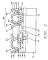
- FIG. 2 shows how the interconnect aspect of U.S. Pat. No. 6,383,916, can be modified to form an inductor on the surface of the thick layer 20 of polyimide.
- the inductor is created in a plane that is parallel with the surface of the substrate 10 whereby this plane however is separated from the surface of the substrate 10 by the combined heights of layers 12 , 14 , 18 , and 20 .
- FIG. 2 shows a cross section 40 of the inductor taken in a plane that is perpendicular to the surface of substrate 10 .
- the wide and thick metal will also contribute to a reduction of the resistive energy losses.
- the low resistivity metal such as gold, silver and copper, can be applied using electroplating, the thickness can be about 20 ⁇ m.
- the electromagnetic field in the silicon substrate will be reduced as the distance is increased, and the Q value of the inductor can be increased.
- the inductor overlies the layer of passivation and by, in addition, creating the inductor on the surface of a thick layer of dielectric (such as a polymer) formed over the passivation layer.
- a thick layer of dielectric such as a polymer
- the openings 19 in passivation layer 18 may be as small as 0.1 um wide.
- contact pads 16 may also be nearly as small, which allows for greater routing capability in the top fine-line metallization layer, and lower capacitance.
- the openings 22 / 36 / 38 in polymer 20 are larger than the passivation openings 19 .
- the polymer openings 22 / 36 / 38 are aligned with passivation openings 19 .
- the larger polymer openings allow for relaxed design rules, simpler opening formation, and the use of a thick metal layer for the post-passivation metallization of the invention.
- FIG. 2 illustrates interconnect structure 26 as well as inductor 40 , wherein the inductor includes two contacts 41 and 43 , through polymer layer 20 to contact pads 16 .
- FIG. 2 structure may be covered by an additional layer of polymer (not shown).
- FIGS. 24 a and 24 b illustrate another feature of the invention, in which contacts to the inductor are formed in a different manner than the 2 downward contacts of FIG. 2 .
- a layer 35 of dielectric, preferably polyimide or the like is deposited over interconnection 26 and inductor 40 .
- An opening 36 ′ to one end of the inductor is then formed to expose one terminal of the inductor 40 .
- Inductor 40 in FIG. 24 a thus can have one contact extending upward, and a second contact 40 ′ extending downward, in a “one-up, one-down” configuration.
- FIG. 24 b illustrates another alternative, in which 2 upward contact openings 36 ′ and 38 ′ are formed from inductor 40 , in a “two-up” configuration.
- the upward contacts may be used for connection to external devices or packaging, by way of wire bonding, solder bumps, or the like.
- wire bonding an upper surface of inductor 40 must be formed of a wire-bondable material such as Au or Al.
- solder bump connection under bump metallization (UBM) would be formed in the upward contact opening, followed by solder bump formation.
- UBM under bump metallization
- interconnections to other contact pads on the same die may be made through openings 36 ′ and/or 38 ′, using similar metallization (but as an additional layer) as used for structure 26 and inductor 40 .
- extension 89 connected to inductor 40 , is used to relocate an inductor contact opening 36 ′′ to another location on the die, such as at the die edge. This may be useful for ease of wire bonding, for example. Opening 38 ′′ is formed as earlier described. Extension 89 is formed at the same time and of the same metallization as structure 26 and inductor 40 .
- extension 89 could be used to interconnect inductor 40 to another contact point on the same die, by making a downward contact (not shown, but described earlier) instead of upward contact 36 ′′.
- FIG. 3 shows a top view 42 of the spiral structure of the inductor 40 that has been created on the surface of layer 20 of dielectric.
- the inductor 40 cross section that is shown in FIG. 2 is taken along line 2 - 2 of FIG. 3 .
- FIG. 4 shows a cross section of inductor 40 whereby the inductor has been further isolated from the surface of the substrate 10 by the addition of a conductive plate 44 ′, of conducting material, formed under substantially all of the inductor, and preferably formed of Cu (copper) or Au (gold).
- the surface area of the conductive plate 44 ′ typically extends over the surface of passivation layer 18 such that the inductor 40 aligns with and overlays the conductive plate 44 ′, the surface area of conductive plate 44 ′ can be extended slightly beyond these boundaries to further improve shielding the surface of substrate 10 from the electromagnetic field of inductor 40 .
- Conductive plate 44 ′ can be connected to one of the inductor terminals (as shown in FIG. 4 , in which it is connected to the rightmost inductor terminal 43 ), or may be left at a floating voltage level, or may be connected to another voltage level, deciding on the system's electrical design.
- Conductive plate 44 ′ is formed using the methods and material of the invention, as later described with regard to the metal layer used to form metal interconnect 26 and inductor 40 . Conductive plate 44 ′ is formed at the same time as connectors 44 , which serve to connect the next level metal to contact points 16 , as shown in FIG. 4 .
- a second polymer layer 47 may be deposited over inductor 40 and interconnect structure 26 , to provide additional protection of the metal structures.
- a substrate 80 is shown, which could be an underlying dielectric layer, and a metal contact point 81 , preferably comprising aluminum.
- a layer 84 of passivation has been patterned creating an opening 82 through layer 84 that exposes the contact pad 81 .
- Layer 86 is a layer of polymer, preferably polyimide, as earlier described, deposited over the layer 84 of passivation, including the exposed surface of the contact pad.
- Polymer layer 86 such as polyimide, is typically spun on. For some thick layers of polymer, the polymer can be screen printed. Alternately, a laminated dry film polymer may be used.
- FIG. 13 illustrates forming an opening 87 in polymer 86 , wherein the polymer opening 87 is larger than passivation opening 82 .
- Opening 87 is depicted having sloped sides 85 .
- Polymer layer 86 is exposed and developed to form opening 87 , which initially has vertical sidewalls. However, the subsequent curing process causes the sidewalls to have a slope 85 , and a opening 87 to have a resultant partially conical shape.
- the sidewall slope 85 may have an angle of 45 degrees or more, and is typically between about 50 and 60 degrees. It may be possible to form the sidewalls with an angle as small as 20 degrees.
- a glue/barrier layer 88 preferably comprising TiW, is deposited, preferably by sputtering to a thickness of between about 500 and 5,000 Angstroms.
- a gold seed layer 90 is next sputter deposited over the glue/barrier 88 , to a thickness of between about 300 and 3,000 Angstroms.
- a bulk layer 92 of gold (Au) is next formed by electroplating, to a thickness of between about 1 and 20 ⁇ m. Electroplating is preceded by deposition of a thick photoresist 94 (to a thickness greater than the desired bulk metal thickness), and conventional lithography to expose the gold seed layer 90 in those areas where electroplating thick metallization is desired.
- photoresist 94 is removed, as shown in FIG. 15 .
- Glue/barrier Layer 88 and gold seed layer 90 are now removed, as shown in FIG. 16 , by etching, using bulk Au layer 92 as a mask.
- One coil of inductor 40 is shown, but it would be understood that the complete inductor would be formed at the same time.
- polymer opening 87 may be only partially filled, as shown in FIGS. 17-18 , which provides tight design rules for fine-pitch inductors.
- the design rule of polymer opening 87 is typically about 15 um, while the metal traces of inductor are as tight as a 4 um pitch. Therefore, patterning metal inside the polyimide opening is a very important feature of this technology.
- Glue/barrier layer 88 and Au seed layer 90 are sputtered as previously described, and photoresist 95 formed as shown in FIG. 17 , followed by electroplating gold bulk layer 92 . Photoresist 95 is then stripped, and the seed layer and glue/barrier etched as previously described, and as shown in FIG. 18 .
- copper may be used as the bulk metal in the post-passivation metallization scheme.
- the FIG. 13 structure is a starting point.
- a glue/barrier layer 100 of Cr or Ti is sputter deposited to a thickness of between about 200 and 2000 Angstroms.
- a Cu seed layer 102 is sputter deposited to a thickness of between about 2,000 and 10,000 Angstroms.
- Bulk layer 104 of Cu is next electroplated to a thickness of between about 3 and 20 ⁇ m, also using a photoresist 94 ′ and conventional lithography to define the areas to be electroplated.
- an optional cap layer 106 comprising Ni may also be formed, also by electroplating, to a thickness of between about 0.1 and 3 um.
- photoresist 94 ′ is stripped, exposing Cu seed layer 104 .
- Glue/barrier layer 100 and Cu seed layer 102 are now removed, as shown in FIG. 21 , by etching.
- the bulk Cu layer 104 is used as a mask for this etch.
- Ni cap layer 106 acts as an etch stop during the etching of glue/barrier 100 and seed layer 102 .
- a faster Cu etch recipe can be used for removing the seed layer since there is no loss of Cu bulk in this configuration.
- polymer opening 87 may be only partially filled, as shown in FIGS. 22-23 .
- Glue/barrier layer 100 and Cu seed layer 102 are sputtered as previously described, and photoresist 95 ′ formed as shown in FIG. 22 , followed by electroplating Cu bulk layer 104 and Ni 106 .
- Photoresist 95 ′ is then stripped, and the seed layer and glue/barrier etched as previously described, and as shown in FIG. 23 .
- inductor 19 has been created on the surface of layer 18 of passivation.
- the ohmic resistivity of the metal that is used for inductor 19 must be as low as possible. For this reason, the use of a thick layer of, for instance, gold is preferred for the formation of inductor 19 . It has been shown that a thick layer of gold increased the Q value of inductor 19 from about 5 to about 20 for 2.4 GHz applications.
- FIG. 5 a inductor may be connected to other elements in various configurations, as earlier described. These include both terminals being connected to lower levels, as shown in FIG. 4 , one up and one down as shown in FIG. 24 a , or both up as in FIG. 24 b.
- An additional layer of polymer may optionally be formed over inductor 19 .
- polymer islands may be formed only under the inductor coils, and not elsewhere over the passivation layer, in order to reduce the stress caused by a larger sheet of polymer.
- FIGS. 5 b - 5 c are a cross-sectional representation, and top view, respectively, of inductors of the invention formed on polymer islands.
- Each island may contain one or more than one inductor, such as on the right-most island of FIG. 5 c having a first inductor 40 ′ and second inductor 40 ′′′.
- isolated islands of polymer 20 ′ are formed, by depositing a polymer layer and then patterning the polymer layer to form the polymer islands.
- the polymer islands may also be formed by screen printing, or by dry film lamination.
- the islands of polymer 20 ′ are formed only at the location of inductors 40 ′ and 40 ′′, which are formed subsequent to polymer island formation.
- inductors 40 ′ and 40 ′′ of FIG. 5 b are formed as earlier described.
- inductor 40 ′′ is shown with downward contacts 41 ′ and 43 ′ connecting to metal contact points 16 .
- Inductors 40 ′ are shown without contacts but could be connected upward for connection to external circuits, as described elsewhere.
- FIG. 5 c is a top view of the inductors of the invention shown in FIG. 5 b , in which the FIG. 5 b cross-section is taken along line 5 b - 5 b in FIG. 5 c . It can be seen in FIG. 5 c that polymer islands 20 ′ are isolated from one another, and polymer is only located under inductor locations—passivation layer 18 is exposed in all other areas of the substrate.
- An additional protective layer of polymer may optionally be formed over inductors 40 ′ and 40 ′′.
- polymer islands may be formed under other devices of the invention, including passive devices such as resistors and capacitors.
- FIGS. 6 a - 6 b depict a transformer made according to the invention.
- the transformer consists of bottom coil 60 , and top coil 62 , isolated by a dielectric layer 47 .
- Polymer layers 20 , and 64 are formed, and comprise materials, previously described. Openings 66 are provided in top polymer layer 64 for connections to the top coil 62 .
- FIG. 6 b is a cross-sectional representation of a transformer of the invention, in which the bottom coil 60 is formed directly on passivation layer 18 .
- FIG. 6 c is a three-dimensional view of a solenoid structure of an inductor 19 that has been created on passivation layer 18 , according to the invention. Further highlighted in FIG. 6 c are:
- FIG. 6 d is a three dimensional view of a solenoid that has been created on a first layer 29 of polymer, having vias 23 created in a second layer of polymer.
- FIG. 6 e is a top view of the solenoid of FIGS. 6 c and 6 d . Vias 23 are shown, connecting top metal segments 27 to bottom metal segments 25 .
- FIG. 6 f is a cross section of the structure of FIGS. 6 c - e , taken along line 6 f - 6 f ′ of FIG. 6 e.
- FIGS. 6 g - 6 h a toroidal inductor 68 is shown, also formed according to the method and structure of the invention.
- FIG. 6 g a three-dimensional view is shown, including top metal wires 27 ′, with vias 23 ′ connecting the top metal wires to the bottom metal wires 25 ′.
- FIG. 6 h shows, for further clarification, a top view of the toroidal inductor 68 of FIG. 6 g .
- the highlighted features of this figure have previously been explained and therefore do not need to be further discussed at this time.
- FIG. 7 a is a cross section of a capacitor that has been created over a substrate 10 .
- a layer (or layers) 14 of conductive interconnect lines and contact points 16 have been created over substrate 10 .
- a layer 18 of passivation has been deposited over layer 14 , with openings created in layer 18 of passivation through which contact pads 16 can be accessed.
- a capacitor contains, as is well known, a lower plate, an upper plate and a layer of dielectric that separates the upper plate from the lower plate.
- FIG. 7 a includes lower plate 42 , upper plate 45 , and dielectric layer 46 .
- the upper and lower plates are formed as earlier described, using electroplated Au or Cu for the bulk metals.
- An optional protective polymer, preferably polyimide, may be formed over the capacitor. Contacts to the capacitor may be made as described earlier for inductor terminals (both down, one up and one down, or both up).
- Lower plate 42 is formed to a thickness of between about 0.5 and 20 ⁇ m.
- Layer 46 of dielectric is between about 500 and 50,000 Angstroms.
- Upper plate 45 is between about 0.5 and 20 ⁇ m thick.
- the post-passivation capacitor shown in cross section in FIG. 7 a has:
- the capacitor of FIG. 7 a may alternately be formed above a polymer layer (deposited over passivation 18 ), similar to the inductor of FIG. 4 .
- Dielectric layer 46 is formed of a high-K dielectric material such as Si 3 N 4 , TEOS, Ta 2 O 5 , TiO 2 , SrTiO 3 , or SiON, which are typically deposited by CVD (Chemical Vapor Deposition).
- CVD Chemical Vapor Deposition
- the dielectric layer 46 can be a polymer film, including polyimide, benzocyclobutene (BCB), parylene or an epoxy-based material such as photoepoxy SU-8.
- a polymer film including polyimide, benzocyclobutene (BCB), parylene or an epoxy-based material such as photoepoxy SU-8.
- FIGS. 7 b - 7 c show a cross section where, as in FIG. 7 a , a capacitor is created.
- a thick layer 20 of polymer has been deposited over the surface of the passivation layer 18 and has been patterned in order to make the contact pads 16 accessible though the thick layer 20 of polymer.
- FIG. 7 b shows the polymer vias having a smaller via diameter than the vias created through the layer of passivation. It is however preferred, as shown in FIG. 7 c , that larger vias be used in conjunction with smaller passivation vias.
- the thick layer 20 of polymer moves most of the capacitor, that is the lower plate 42 , the upper plate 45 and the dielectric 46 , further from the surface of substrate 10 by a distance equal to the thickness of layer 20 .
- the range of polyimide thickness can vary from 2 ⁇ m to 150 ⁇ m, depending on electrical design requirements. This leads to a significant increase in distance between the capacitor and underlying structures, including metal lines and/or the silicon substrate, so that parasitic capacitance is significantly reduced.
- FIGS. 7 a - 7 c depict both capacitor terminals being connected down to a lower layer.
- the capacitor may also be contacted in one-up-one-down configuration—as shown in FIG. 25 —or a two-up technique, as previously described with reference to FIG. 24 b.
- the upper capacitor plate 45 can be connected in an upward manner through a layer of dielectric that has been deposited over the second capacitor plate 45 of FIGS. 7 a - 7 c .
- This is further highlighted in the cross section of FIG. 25 wherein a layer 35 of dielectric has been deposited over the capacitor upper plate 45 , with an opening 37 created through the layer 35 of dielectric to expose the capacitor upper plate 45 , for further connection to external circuits.
- the capacitor of FIGS. 7 a - 7 c may optionally be covered with a protective layer of polymer, as previously described.
- FIG. 8 shows a cross section of a substrate 10 over which has been deposited a layer 18 of passivation, with a resistor 48 formed over passivation layer 18 .
- a resistor as is well known, is created by connecting two points with a material that offers electrical resistance to the passage of current through the material.
- a resistive material such as TaN, NiCr, NiSn, tungsten (W), TiW, TiN, Cr, Ti, TaSi or Ni.
- tungsten (W) TiW
- TiN TiN
- Cr Ti
- TaSi or Ni tungsten
- Resistor dimensions such as thickness, length and width of deposition of high resistive material 48 are application dependent.
- the resistor that is shown in cross section in FIG. 8 is, as are the capacitors of FIGS. 7 a - 7 c , created in a post-passivation process on the surface of layer 18 of passivation.
- FIGS. 9 a - 9 b shows the resistor of the invention formed over a thick layer of polymer 20 , connected to contact pads 16 .
- FIGS. 8 , 9 a and 9 b show a “two-down” system for contacting the terminals of the resistor 48 .
- the resistor may also be contacted in one-up-one-down configuration, as shown in FIG. 26 , or a two-up technique, as previously described with reference to the inductor of FIG. 24 b.
- An additional layer of polymer, to protect the resistor, may optionally be formed over the resistor of FIGS. 8 , 9 a and 9 b.
- Interconnect metal 50 of the invention is formed in polymer openings, as previously described, which are aligned with smaller passivation openings, to connect to pads 16 , and serves as an under-bump metal (UBM).
- UBM under-bump metal
- Solder contact bumps are formed over UBM 50 using conventional methods of selective solder deposition (plating, ball mounting, or screen printing on the surface of contacts 50 ), the application of a flux on the deposited solder and flowing the solder.
- a discrete device 54 is connected to solder balls 52 and has solder 53 to facilitate the connection. This is similar to the surface mount technology used in the assembly of printed circuit boards.
- the discrete electrical component may be, but is not limited to, devices such as inductors, capacitors or resistors.
- FIG. 11 illustrates mounting of discrete device 54 , using solder bumps 56 , and UBM 50 , directly over passivation layer 18 .
- UBM 50 is formed using the metallization scheme of the invention (as shown and described with respect to FIGS. 12-23 ), except that when Au is used as the bulk layer, its thickness is in the range of between about 0.1 and 20 um, the thinner range being preferable to avoid a high gold concentration in the solder near the UBM/solder interface, after processing.
- the present invention by contrast, can use easily formed thick metal layers, the thickness reducing resistance.
- Use of polymer 20 further separates the components formed from underlying structures, reducing capacitance. With the reduced capacitance, a higher frequency of operation results due to a higher resonant frequency.
Landscapes
- Semiconductor Integrated Circuits (AREA)
- Internal Circuitry In Semiconductor Integrated Circuit Devices (AREA)
Abstract
Description
-
- 23, vias that are created in the thick layer of
polymer 20, having substantially vertical metal segments - 25, the bottom metal segments of the solenoid
- 27, the top metal segments of the solenoid.
The top andbottom metal segments vias 23, to form a continuous solenoid.
- 23, vias that are created in the thick layer of
-
- reduced parasitic capacitance between the capacitor and the underlying silicon substrate
- allowed for the use of a thick layer of conductive material for the capacitor plates, reducing the resistance of the capacitor; this is particularly important for wireless applications
- can use high-dielectric-constant material such as TiO2 or Ta2O5, in addition to polymer, Si3N4 or SiO2, for the dielectric between the upper and the lower plate of the capacitor, resulting in a higher capacitive value of the capacitor.
-
- The discrete components of
FIGS. 10 and 11 have the advantages of performance and cost savings since the discrete component does not have to be mounted on a Printed Circuit Board as is the common practice in the art.
- The discrete components of
-
- the discrete components provide optimized parameters and can be mounted close to the circuits, which offer true system-on-chip performance
- the discrete components mounting close to the circuits also minimizes parasitics
- the post-passivation process of the invention allows for the selection of discrete component design parameters that result in reduced resistance of the discrete capacitor and the discrete inductor, this is further clear from the following comparison between prior art processes and the processes of the invention.
Prior approaches in the art uses thinner metal for inductors, requiring wider coils (to minimize resistance), resulting in increased surface area, increasing the parasitic capacitance of the inductor and causing eddy current losses in the surface of the substrate.
Claims (63)
Priority Applications (1)
| Application Number | Priority Date | Filing Date | Title |
|---|---|---|---|
| US11/062,276 US8089155B2 (en) | 1998-12-21 | 2005-02-18 | High performance system-on-chip discrete components using post passivation process |
Applications Claiming Priority (9)
| Application Number | Priority Date | Filing Date | Title |
|---|---|---|---|
| US21679198A | 1998-12-21 | 1998-12-21 | |
| US09/251,183 US6383916B1 (en) | 1998-12-21 | 1999-02-17 | Top layers of metal for high performance IC's |
| US63792600A | 2000-08-14 | 2000-08-14 | |
| US09/721,722 US6303423B1 (en) | 1998-12-21 | 2000-11-27 | Method for forming high performance system-on-chip using post passivation process |
| US09/970,005 US6455885B1 (en) | 1998-12-21 | 2001-10-03 | Inductor structure for high performance system-on-chip using post passivation process |
| US10/156,590 US6489647B1 (en) | 1998-12-21 | 2002-05-28 | Capacitor for high performance system-on-chip using post passivation process structure |
| US10/303,451 US6897507B2 (en) | 1998-12-21 | 2002-11-25 | Capacitor for high performance system-on-chip using post passivation device |
| US10/445,560 US6869870B2 (en) | 1998-12-21 | 2003-05-27 | High performance system-on-chip discrete components using post passivation process |
| US11/062,276 US8089155B2 (en) | 1998-12-21 | 2005-02-18 | High performance system-on-chip discrete components using post passivation process |
Related Parent Applications (1)
| Application Number | Title | Priority Date | Filing Date |
|---|---|---|---|
| US10/445,560 Division US6869870B2 (en) | 1998-12-21 | 2003-05-27 | High performance system-on-chip discrete components using post passivation process |
Publications (2)
| Publication Number | Publication Date |
|---|---|
| US20050230783A1 US20050230783A1 (en) | 2005-10-20 |
| US8089155B2 true US8089155B2 (en) | 2012-01-03 |
Family
ID=46204843
Family Applications (3)
| Application Number | Title | Priority Date | Filing Date |
|---|---|---|---|
| US10/445,560 Expired - Lifetime US6869870B2 (en) | 1998-12-21 | 2003-05-27 | High performance system-on-chip discrete components using post passivation process |
| US11/062,276 Expired - Fee Related US8089155B2 (en) | 1998-12-21 | 2005-02-18 | High performance system-on-chip discrete components using post passivation process |
| US11/062,277 Expired - Lifetime US8129265B2 (en) | 1998-12-21 | 2005-02-18 | High performance system-on-chip discrete components using post passivation process |
Family Applications Before (1)
| Application Number | Title | Priority Date | Filing Date |
|---|---|---|---|
| US10/445,560 Expired - Lifetime US6869870B2 (en) | 1998-12-21 | 2003-05-27 | High performance system-on-chip discrete components using post passivation process |
Family Applications After (1)
| Application Number | Title | Priority Date | Filing Date |
|---|---|---|---|
| US11/062,277 Expired - Lifetime US8129265B2 (en) | 1998-12-21 | 2005-02-18 | High performance system-on-chip discrete components using post passivation process |
Country Status (1)
| Country | Link |
|---|---|
| US (3) | US6869870B2 (en) |
Cited By (6)
| Publication number | Priority date | Publication date | Assignee | Title |
|---|---|---|---|---|
| US20090180002A1 (en) * | 2002-07-15 | 2009-07-16 | Olympus Corporation | White balance processing apparatus and processing method thereof |
| US20150279546A1 (en) * | 2014-03-31 | 2015-10-01 | International Business Machines Corporation | Thin film inductor with extended yokes |
| US20180308795A1 (en) * | 2017-04-20 | 2018-10-25 | Renesas Electronics Corporation | Semiconductor device and method of manufacturing the same |
| US11201602B1 (en) | 2020-09-17 | 2021-12-14 | Analog Devices, Inc. | Apparatus and methods for tunable filtering |
| US11201600B1 (en) | 2020-10-05 | 2021-12-14 | Analog Devices, Inc. | Apparatus and methods for control and calibration of tunable filters |
| US11404197B2 (en) * | 2017-06-09 | 2022-08-02 | Analog Devices Global Unlimited Company | Via for magnetic core of inductive component |
Families Citing this family (59)
| Publication number | Priority date | Publication date | Assignee | Title |
|---|---|---|---|---|
| US9219755B2 (en) | 1996-11-08 | 2015-12-22 | Finjan, Inc. | Malicious mobile code runtime monitoring system and methods |
| US8079086B1 (en) | 1997-11-06 | 2011-12-13 | Finjan, Inc. | Malicious mobile code runtime monitoring system and methods |
| US7058822B2 (en) | 2000-03-30 | 2006-06-06 | Finjan Software, Ltd. | Malicious mobile code runtime monitoring system and methods |
| US6869870B2 (en) * | 1998-12-21 | 2005-03-22 | Megic Corporation | High performance system-on-chip discrete components using post passivation process |
| US7531417B2 (en) * | 1998-12-21 | 2009-05-12 | Megica Corporation | High performance system-on-chip passive device using post passivation process |
| US8421158B2 (en) * | 1998-12-21 | 2013-04-16 | Megica Corporation | Chip structure with a passive device and method for forming the same |
| US6303423B1 (en) | 1998-12-21 | 2001-10-16 | Megic Corporation | Method for forming high performance system-on-chip using post passivation process |
| US8178435B2 (en) | 1998-12-21 | 2012-05-15 | Megica Corporation | High performance system-on-chip inductor using post passivation process |
| US6936531B2 (en) * | 1998-12-21 | 2005-08-30 | Megic Corporation | Process of fabricating a chip structure |
| US7271489B2 (en) * | 2003-10-15 | 2007-09-18 | Megica Corporation | Post passivation interconnection schemes on top of the IC chips |
| DE10231385B4 (en) * | 2001-07-10 | 2007-02-22 | Samsung Electronics Co., Ltd., Suwon | Semiconductor chip with bond pads and associated multi-chip package |
| US6759275B1 (en) * | 2001-09-04 | 2004-07-06 | Megic Corporation | Method for making high-performance RF integrated circuits |
| US7932603B2 (en) | 2001-12-13 | 2011-04-26 | Megica Corporation | Chip structure and process for forming the same |
| US8368150B2 (en) * | 2003-03-17 | 2013-02-05 | Megica Corporation | High performance IC chip having discrete decoupling capacitors attached to its IC surface |
| TWI236763B (en) * | 2003-05-27 | 2005-07-21 | Megic Corp | High performance system-on-chip inductor using post passivation process |
| CN1291069C (en) * | 2003-05-31 | 2006-12-20 | 香港科技大学 | Electroplating preparation method of fine-pitch flip-chip bumps |
| TWI225280B (en) * | 2003-06-30 | 2004-12-11 | Advanced Semiconductor Eng | Bumping process |
| US7470997B2 (en) | 2003-07-23 | 2008-12-30 | Megica Corporation | Wirebond pad for semiconductor chip or wafer |
| US7148535B2 (en) * | 2003-08-25 | 2006-12-12 | Lsi Logic Corporation | Zero capacitance bondpad utilizing active negative capacitance |
| US20050046022A1 (en) * | 2003-08-26 | 2005-03-03 | Micrel, Incorporated | Semiconductor devices integrated with wafer-level packaging |
| US7394161B2 (en) * | 2003-12-08 | 2008-07-01 | Megica Corporation | Chip structure with pads having bumps or wirebonded wires formed thereover or used to be tested thereto |
| JP4675050B2 (en) * | 2004-03-16 | 2011-04-20 | 株式会社リコー | Semiconductor device |
| US7423346B2 (en) * | 2004-09-09 | 2008-09-09 | Megica Corporation | Post passivation interconnection process and structures |
| US8008775B2 (en) | 2004-09-09 | 2011-08-30 | Megica Corporation | Post passivation interconnection structures |
| US7355282B2 (en) | 2004-09-09 | 2008-04-08 | Megica Corporation | Post passivation interconnection process and structures |
| US8384189B2 (en) * | 2005-03-29 | 2013-02-26 | Megica Corporation | High performance system-on-chip using post passivation process |
| US7470927B2 (en) | 2005-05-18 | 2008-12-30 | Megica Corporation | Semiconductor chip with coil element over passivation layer |
| TWI305951B (en) * | 2005-07-22 | 2009-02-01 | Megica Corp | Method for forming a double embossing structure |
| US7410894B2 (en) * | 2005-07-27 | 2008-08-12 | International Business Machines Corporation | Post last wiring level inductor using patterned plate process |
| JP2007059878A (en) * | 2005-07-27 | 2007-03-08 | Seiko Epson Corp | Semiconductor device and oscillator |
| US7521705B2 (en) * | 2005-08-15 | 2009-04-21 | Micron Technology, Inc. | Reproducible resistance variable insulating memory devices having a shaped bottom electrode |
| US7473999B2 (en) * | 2005-09-23 | 2009-01-06 | Megica Corporation | Semiconductor chip and process for forming the same |
| US20070114663A1 (en) * | 2005-11-23 | 2007-05-24 | Brown Derrick L | Alloys for flip chip interconnects and bumps |
| US7990037B2 (en) | 2005-11-28 | 2011-08-02 | Megica Corporation | Carbon nanotube circuit component structure |
| US7569422B2 (en) | 2006-08-11 | 2009-08-04 | Megica Corporation | Chip package and method for fabricating the same |
| US7807511B2 (en) * | 2006-11-17 | 2010-10-05 | Freescale Semiconductor, Inc. | Method of packaging a device having a multi-contact elastomer connector contact area and device thereof |
| US7588951B2 (en) * | 2006-11-17 | 2009-09-15 | Freescale Semiconductor, Inc. | Method of packaging a semiconductor device and a prefabricated connector |
| US7696016B2 (en) * | 2006-11-17 | 2010-04-13 | Freescale Semiconductor, Inc. | Method of packaging a device having a tangible element and device thereof |
| US8749021B2 (en) * | 2006-12-26 | 2014-06-10 | Megit Acquisition Corp. | Voltage regulator integrated with semiconductor chip |
| US7659192B2 (en) * | 2006-12-29 | 2010-02-09 | Intel Corporation | Methods of forming stepped bumps and structures formed thereby |
| US8178965B2 (en) * | 2007-03-14 | 2012-05-15 | Infineon Technologies Ag | Semiconductor module having deflecting conductive layer over a spacer structure |
| US7923645B1 (en) | 2007-06-20 | 2011-04-12 | Amkor Technology, Inc. | Metal etch stop fabrication method and structure |
| US7951697B1 (en) | 2007-06-20 | 2011-05-31 | Amkor Technology, Inc. | Embedded die metal etch stop fabrication method and structure |
| KR101185886B1 (en) * | 2007-07-23 | 2012-09-25 | 삼성전자주식회사 | Semiconductor chip, semiconductor package, card and system having universal interconnection lines |
| US7958626B1 (en) * | 2007-10-25 | 2011-06-14 | Amkor Technology, Inc. | Embedded passive component network substrate fabrication method |
| JP5578797B2 (en) * | 2009-03-13 | 2014-08-27 | ルネサスエレクトロニクス株式会社 | Semiconductor device |
| US8143952B2 (en) * | 2009-10-08 | 2012-03-27 | Qualcomm Incorporated | Three dimensional inductor and transformer |
| US9064712B2 (en) * | 2010-08-12 | 2015-06-23 | Freescale Semiconductor Inc. | Monolithic microwave integrated circuit |
| US8791501B1 (en) | 2010-12-03 | 2014-07-29 | Amkor Technology, Inc. | Integrated passive device structure and method |
| US8822327B2 (en) * | 2012-08-16 | 2014-09-02 | Infineon Technologies Ag | Contact pads with sidewall spacers and method of making contact pads with sidewall spacers |
| RU2512724C2 (en) * | 2013-03-01 | 2014-04-10 | Борис Николаевич Дьяков | Electrolyser for separation of low-melting alloys by means of electrolysis in molten salts into selective concentrates |
| US9006584B2 (en) * | 2013-08-06 | 2015-04-14 | Texas Instruments Incorporated | High voltage polymer dielectric capacitor isolation device |
| JP6418755B2 (en) * | 2014-02-27 | 2018-11-07 | シーメンス アクチエンゲゼルシヤフトSiemens Aktiengesellschaft | Electrode having UBM structure and manufacturing method thereof |
| US20150276945A1 (en) | 2014-03-25 | 2015-10-01 | Oy Ajat Ltd. | Semiconductor bump-bonded x-ray imaging device |
| US9576923B2 (en) * | 2014-04-01 | 2017-02-21 | Ati Technologies Ulc | Semiconductor chip with patterned underbump metallization and polymer film |
| US10269904B2 (en) * | 2014-10-31 | 2019-04-23 | Taiwan Semiconductor Manufacturing Company Ltd. | Semiconductor structure and manufacturing method thereof |
| US10269703B2 (en) * | 2016-11-29 | 2019-04-23 | Taiwan Semiconductor Manufacturing Company Ltd. | Semiconductor device and method of forming the same |
| JP6888581B2 (en) * | 2018-04-11 | 2021-06-16 | 株式会社デンソー | Semiconductor devices and their manufacturing methods |
| TWI697078B (en) * | 2018-08-03 | 2020-06-21 | 欣興電子股份有限公司 | Package substrate structure and method of bonding using the same |
Citations (107)
| Publication number | Priority date | Publication date | Assignee | Title |
|---|---|---|---|---|
| US4021838A (en) | 1974-11-20 | 1977-05-03 | International Business Machines Corporation | Semiconductor integrated circuit devices |
| US4598307A (en) | 1982-09-22 | 1986-07-01 | Fujitsu Limited | Integrated circuit device having package with bypass capacitor |
| US4685998A (en) | 1984-03-22 | 1987-08-11 | Thomson Components - Mostek Corp. | Process of forming integrated circuits with contact pads in a standard array |
| US4885841A (en) | 1989-02-21 | 1989-12-12 | Micron Technology, Inc. | Vibrational method of aligning the leads of surface-mount electronic components with the mounting pads of printed circuit boards during the molten solder mounting process |
| US5049979A (en) | 1990-06-18 | 1991-09-17 | Microelectronics And Computer Technology Corporation | Combined flat capacitor and tab integrated circuit chip and method |
| US5055907A (en) | 1989-01-25 | 1991-10-08 | Mosaic, Inc. | Extended integration semiconductor structure with wiring layers |
| US5095402A (en) | 1990-10-02 | 1992-03-10 | Rogers Corporation | Internally decoupled integrated circuit package |
| US5106461A (en) | 1989-04-04 | 1992-04-21 | Massachusetts Institute Of Technology | High-density, multi-level interconnects, flex circuits, and tape for tab |
| US5182172A (en) | 1991-04-18 | 1993-01-26 | Bausch & Lomb Incorporated | Post-plating passivation treatment |
| US5212403A (en) | 1990-09-10 | 1993-05-18 | Hitachi, Ltd. | Integrated circuit device having an ic chip mounted on the wiring substrate and having suitable mutual connections between internal circuits |
| US5226232A (en) | 1990-05-18 | 1993-07-13 | Hewlett-Packard Company | Method for forming a conductive pattern on an integrated circuit |
| US5370766A (en) | 1993-08-16 | 1994-12-06 | California Micro Devices | Methods for fabrication of thin film inductors, inductor networks and integration with other passive and active devices |
| US5372967A (en) | 1992-01-27 | 1994-12-13 | Motorola, Inc. | Method for fabricating a vertical trench inductor |
| US5416356A (en) | 1993-09-03 | 1995-05-16 | Motorola, Inc. | Integrated circuit having passive circuit elements |
| US5478773A (en) | 1994-04-28 | 1995-12-26 | Motorola, Inc. | Method of making an electronic device having an integrated inductor |
| US5501006A (en) | 1993-09-22 | 1996-03-26 | Motorola, Inc. | Method for connection of signals to an integrated circuit |
| US5519582A (en) | 1992-10-05 | 1996-05-21 | Fuji Electric Co., Ltd. | Magnetic induction coil for semiconductor devices |
| US5527998A (en) * | 1993-10-22 | 1996-06-18 | Sheldahl, Inc. | Flexible multilayer printed circuit boards and methods of manufacture |
| US5576680A (en) | 1994-03-01 | 1996-11-19 | Amer-Soi | Structure and fabrication process of inductors on semiconductor chip |
| US5608262A (en) | 1995-02-24 | 1997-03-04 | Lucent Technologies Inc. | Packaging multi-chip modules without wire-bond interconnection |
| US5629240A (en) | 1994-12-09 | 1997-05-13 | Sun Microsystems, Inc. | Method for direct attachment of an on-chip bypass capacitor in an integrated circuit |
| US5635767A (en) | 1995-06-02 | 1997-06-03 | Motorola, Inc. | Semiconductor device having built-in high frequency bypass capacitor |
| US5686764A (en) | 1996-03-20 | 1997-11-11 | Lsi Logic Corporation | Flip chip package with reduced number of package layers |
| US5742100A (en) | 1995-03-27 | 1998-04-21 | Motorola, Inc. | Structure having flip-chip connected substrates |
| US5763108A (en) | 1997-03-05 | 1998-06-09 | Headway Technologies, Inc. | High saturtion magnetization material and magnetic head fabricated therefrom |
| US5789303A (en) | 1994-11-28 | 1998-08-04 | Northern Telecom Limited | Method of adding on chip capacitors to an integrated circuit |
| US5827776A (en) * | 1996-07-18 | 1998-10-27 | Advanced Micro Devices, Inc. | Method of making an integrated circuit which uses an etch stop for producing staggered interconnect lines |
| US5842626A (en) | 1995-03-31 | 1998-12-01 | Intel Corporation | Method for coupling surface mounted capacitors to semiconductor packages |
| US5884990A (en) | 1996-08-23 | 1999-03-23 | International Business Machines Corporation | Integrated circuit inductor |
| US5930637A (en) | 1997-10-31 | 1999-07-27 | Taiwan Semiconductor Manufacturing Co., Ltd. | Method of fabricating a microwave inductor |
| US5949654A (en) | 1996-07-03 | 1999-09-07 | Kabushiki Kaisha Toshiba | Multi-chip module, an electronic device, and production method thereof |
| US5969422A (en) * | 1997-05-15 | 1999-10-19 | Advanced Micro Devices, Inc. | Plated copper interconnect structure |
| US6008102A (en) | 1998-04-09 | 1999-12-28 | Motorola, Inc. | Method of forming a three-dimensional integrated inductor |
| US6025261A (en) | 1998-04-29 | 2000-02-15 | Micron Technology, Inc. | Method for making high-Q inductive elements |
| US6051489A (en) | 1997-05-13 | 2000-04-18 | Chipscale, Inc. | Electronic component package with posts on the active side of the substrate |
| US6114938A (en) | 1997-11-11 | 2000-09-05 | Murata Manufacturing Co., Ltd. | Variable inductor device |
| US6168854B1 (en) | 1996-12-23 | 2001-01-02 | Nortel Networks Limited | Method of making a printed circuit board having a tin/lead coating |
| US6169030B1 (en) * | 1998-01-14 | 2001-01-02 | Applied Materials, Inc. | Metallization process and method |
| US6180445B1 (en) | 2000-04-24 | 2001-01-30 | Taiwan Semiconductor Manufacturing Company | Method to fabricate high Q inductor by redistribution layer when flip-chip package is employed |
| US6184589B1 (en) | 1996-11-08 | 2001-02-06 | John J. Budnaitis | Constraining ring for use in electronic packaging |
| US6236103B1 (en) | 1999-03-31 | 2001-05-22 | International Business Machines Corp. | Integrated high-performance decoupling capacitor and heat sink |
| US6236101B1 (en) | 1997-11-05 | 2001-05-22 | Texas Instruments Incorporated | Metallization outside protective overcoat for improved capacitors and inductors |
| FR2793943B1 (en) | 1999-05-18 | 2001-07-13 | Memscap | MICRO-COMPONENTS OF THE MICRO-INDUCTANCE OR MICRO-TRANSFORMER TYPE, AND METHOD FOR MANUFACTURING SUCH MICRO-COMPONENTS |
| US6278264B1 (en) | 2000-02-04 | 2001-08-21 | Volterra Semiconductor Corporation | Flip-chip switching regulator |
| US20010016410A1 (en) | 1996-12-13 | 2001-08-23 | Peng Cheng | Method of forming contacts |
| US6303423B1 (en) | 1998-12-21 | 2001-10-16 | Megic Corporation | Method for forming high performance system-on-chip using post passivation process |
| US6329715B1 (en) | 1996-09-20 | 2001-12-11 | Tdk Corporation | Passive electronic parts, IC parts, and wafer |
| US20020017730A1 (en) | 2000-08-11 | 2002-02-14 | Integrated Electronics & Packaging | Semiconductor device |
| US6365498B1 (en) | 1999-10-15 | 2002-04-02 | Industrial Technology Research Institute | Integrated process for I/O redistribution and passive components fabrication and devices formed |
| US6383916B1 (en) | 1998-12-21 | 2002-05-07 | M. S. Lin | Top layers of metal for high performance IC's |
| US6399997B1 (en) | 2000-08-01 | 2002-06-04 | Megic Corporation | High performance system-on-chip using post passivation process and glass substrates |
| US20020068441A1 (en) | 1998-12-21 | 2002-06-06 | Mou-Shiung Lin | Top layers of metal for high performance IC's |
| TW490803B (en) | 2001-01-04 | 2002-06-11 | Megic Corp | Chip structure having outer layer connection on the protection layer |
| US6417089B1 (en) | 2000-01-03 | 2002-07-09 | Samsung Electronics, Co., Ltd. | Method of forming solder bumps with reduced undercutting of under bump metallurgy (UBM) |
| US6424034B1 (en) | 1998-08-31 | 2002-07-23 | Micron Technology, Inc. | High performance packaging for microprocessors and DRAM chips which minimizes timing skews |
| TW497176B (en) | 2000-03-17 | 2002-08-01 | Macronix Int Co Ltd | Passivation film structure on semiconductor wafer |
| TW498492B (en) | 2001-08-02 | 2002-08-11 | Silicon Integrated Sys Corp | Formation method of selective cap layer on copper interconnect |
| US6432479B2 (en) | 1997-12-02 | 2002-08-13 | Applied Materials, Inc. | Method for in-situ, post deposition surface passivation of a chemical vapor deposited film |
| US20020109232A1 (en) | 1998-12-21 | 2002-08-15 | Mou-Shiung Lin | Chip structure and process for forming the same |
| US20020115282A1 (en) | 1998-12-21 | 2002-08-22 | Mou-Shiung Lin | Chip structure and process for forming the same |
| US6441715B1 (en) | 1999-02-17 | 2002-08-27 | Texas Instruments Incorporated | Method of fabricating a miniaturized integrated circuit inductor and transformer fabrication |
| US6445271B1 (en) | 1999-05-28 | 2002-09-03 | Honeywell International Inc. | Three-dimensional micro-coils in planar substrates |
| US20020121692A1 (en) | 2001-03-05 | 2002-09-05 | Megic Corporation | Low fabrication cost, fine pitch and high reliability solder bump |
| US6456183B1 (en) | 1999-02-26 | 2002-09-24 | Memscap And Planhead-Silmag Phs | Inductor for integrated circuit |
| US6459135B1 (en) | 1999-03-23 | 2002-10-01 | Memscap S.A. | Monolithic integrated circuit incorporating an inductive component and process for fabricating such an integrated circuit |
| TW506045B (en) | 2000-08-14 | 2002-10-11 | Megic Corp | Method for forming high performance system-on-chip using post passivation process |
| US6465879B1 (en) | 1999-10-19 | 2002-10-15 | Citizen Watch Co., Ltd. | Structure for mounting semiconductor device, method of mounting same, semiconductor device, and method of fabricating same |
| TW507479B (en) | 2000-04-11 | 2002-10-21 | 3M Innovative Properties Co | Flexible circuit with coverplate layer and overlapping protective layer |
| US6489656B1 (en) | 2001-10-03 | 2002-12-03 | Megic Corporation | Resistor for high performance system-on-chip using post passivation process |
| US20020180064A1 (en) | 2001-06-05 | 2002-12-05 | Chipbond Technology Corporation | Metallized surface wafer level package structure |
| TW513761B (en) | 2001-12-31 | 2002-12-11 | Calitech Co Ltd | Wafer protection method and system |
| US6495442B1 (en) | 2000-10-18 | 2002-12-17 | Magic Corporation | Post passivation interconnection schemes on top of the IC chips |
| US6501169B1 (en) | 1999-11-29 | 2002-12-31 | Casio Computer Co., Ltd. | Semiconductor device which prevents leakage of noise generated in a circuit element forming area and which shields against external electromagnetic noise |
| US6501185B1 (en) | 2001-06-12 | 2002-12-31 | Advanced Interconnect Technology Ltd. | Barrier cap for under bump metal |
| TW519707B (en) | 2001-12-13 | 2003-02-01 | Megic Corp | Chip structure with passivation layer having outer layer connection and its manufacturing process |
| TW519726B (en) | 2001-12-21 | 2003-02-01 | Megic Corp | Chip structure and its process |
| US6515355B1 (en) | 1998-09-02 | 2003-02-04 | Micron Technology, Inc. | Passivation layer for packaged integrated circuits |
| US20030038331A1 (en) | 1999-02-15 | 2003-02-27 | Casio Computer Co., Ltd. | Semiconductor device having a barrier layer |
| US20030037959A1 (en) | 1999-12-21 | 2003-02-27 | Master Raj N. | Organic packages having low tin solder connections |
| US6559528B2 (en) | 2000-02-21 | 2003-05-06 | Matsushita Electric Industrial Co., Ltd. | Semiconductor device and method for the fabrication thereof |
| TW533559B (en) | 2001-12-17 | 2003-05-21 | Megic Corp | Chip package structure and its manufacturing process |
| TW533533B (en) | 2001-01-24 | 2003-05-21 | Hrl Lab Llc | Integrated circuits protected against reverse engineering and method for fabricating the same using etched passivation openings in integrated circuits |
| US6570247B1 (en) * | 1997-12-30 | 2003-05-27 | Intel Corporation | Integrated circuit device having an embedded heat slug |
| US20030121958A1 (en) | 2001-12-28 | 2003-07-03 | Glenn Ratificar | Solder reflow with microwave energy |
| US20030170934A1 (en) | 1998-12-21 | 2003-09-11 | Megic Corporation | Top layers of metal for high performance IC's |
| US20030197283A1 (en) | 2002-04-23 | 2003-10-23 | Shin Choi | Multi-chip package and method for manufacturing the same |
| US20030224613A1 (en) | 2002-05-30 | 2003-12-04 | Lakshmi Narayan Ramanathan | Method of forming a component overlying a semiconductor substrate |
| US20040016948A1 (en) | 1998-12-21 | 2004-01-29 | Megic Corporation | High performance system-on-chip discrete components using post passivation process |
| US20040029404A1 (en) | 1998-12-21 | 2004-02-12 | Megic Corporation | High performance system-on-chip passive device using post passivation process |
| US20040079966A1 (en) | 1998-12-21 | 2004-04-29 | Mou-Shiung Lin | Chip structure and process for forming the same |
| US20040094841A1 (en) | 2002-11-08 | 2004-05-20 | Casio Computer Co., Ltd. | Wiring structure on semiconductor substrate and method of fabricating the same |
| US6756664B2 (en) | 2002-11-22 | 2004-06-29 | Via Technologies, Inc. | Noise eliminating system on chip and method of making same |
| US20040166659A1 (en) | 1998-12-21 | 2004-08-26 | Megic Corporation | Top layers of metal for high performance IC's |
| US20040166661A1 (en) | 2003-02-21 | 2004-08-26 | Aptos Corporation | Method for forming copper bump antioxidation surface |
| US20040183209A1 (en) | 2003-03-17 | 2004-09-23 | Megic Corporation | High performance IC chip having discrete decoupling capacitors attached to its IC surface |
| US20040245580A1 (en) | 1998-12-21 | 2004-12-09 | Mou-Shiung Lin | [chip structure with a passive device and method for forming the same] |
| US6852616B2 (en) | 2000-11-29 | 2005-02-08 | Matsushita Electric Industrial Co., Ltd. | Semiconductor device and method for producing the same |
| US20050032351A1 (en) | 1998-12-21 | 2005-02-10 | Mou-Shiung Lin | Chip structure and process for forming the same |
| US6914331B2 (en) | 2002-05-27 | 2005-07-05 | Matsushita Electric Industrial Co., Ltd. | Semiconductor device having an inductor formed on a region of an insulating film |
| US6921980B2 (en) | 2001-02-16 | 2005-07-26 | Sharp Kabushiki Kaisha | Integrated semiconductor circuit including electronic component connected between different component connection portions |
| US6952049B1 (en) | 1999-03-30 | 2005-10-04 | Ngk Spark Plug Co., Ltd. | Capacitor-built-in type printed wiring substrate, printed wiring substrate, and capacitor |
| US20050250255A1 (en) | 1998-12-21 | 2005-11-10 | Ying-Chih Chen | Over-passivation process of forming polymer layer over IC chip |
| US20050277281A1 (en) | 2004-06-10 | 2005-12-15 | Dubin Valery M | Compliant interconnect and method of formation |
| US20070108551A1 (en) | 2003-05-27 | 2007-05-17 | Megica Corporation | High performance system-on-chip inductor using post passivation process |
| US20080121943A1 (en) | 1998-12-21 | 2008-05-29 | Mou-Shiung Lin | Top layers of metal for integrated circuits |
| US7416971B2 (en) | 2004-09-23 | 2008-08-26 | Megica Corporation | Top layers of metal for integrated circuits |
| US20080233733A1 (en) | 1998-12-21 | 2008-09-25 | Megica Corporation | Method of wire bonding over active area of a semiconductor circuit |
Family Cites Families (22)
| Publication number | Priority date | Publication date | Assignee | Title |
|---|---|---|---|---|
| FR2559297B1 (en) * | 1984-02-03 | 1990-01-12 | Commissariat Energie Atomique | NEW FLIGHT SKATE FOR MAGNETIC RECORDING HEADS |
| IN181811B (en) | 1993-03-11 | 1998-10-03 | Daya Ranjit Senanayake | |
| US5485038A (en) * | 1993-07-15 | 1996-01-16 | Hughes Aircraft Company | Microelectronic circuit substrate structure including photoimageable epoxy dielectric layers |
| US5904545A (en) * | 1993-12-17 | 1999-05-18 | The Regents Of The University Of California | Apparatus for fabricating self-assembling microstructures |
| US6498074B2 (en) * | 1996-10-29 | 2002-12-24 | Tru-Si Technologies, Inc. | Thinning and dicing of semiconductor wafers using dry etch, and obtaining semiconductor chips with rounded bottom edges and corners |
| US6448153B2 (en) * | 1996-10-29 | 2002-09-10 | Tru-Si Technologies, Inc. | Thinning and dicing of semiconductor wafers using dry etch, and obtaining semiconductor chips with rounded bottom edges and corners |
| US8178435B2 (en) * | 1998-12-21 | 2012-05-15 | Megica Corporation | High performance system-on-chip inductor using post passivation process |
| US6683663B1 (en) * | 1999-02-05 | 2004-01-27 | Alien Technology Corporation | Web fabrication of devices |
| AU2373200A (en) * | 1999-02-05 | 2000-08-25 | Alien Technology Corporation | Apparatuses and methods for forming assemblies |
| US6555408B1 (en) * | 1999-02-05 | 2003-04-29 | Alien Technology Corporation | Methods for transferring elements from a template to a substrate |
| US6380729B1 (en) * | 1999-02-16 | 2002-04-30 | Alien Technology Corporation | Testing integrated circuit dice |
| US6468638B2 (en) * | 1999-03-16 | 2002-10-22 | Alien Technology Corporation | Web process interconnect in electronic assemblies |
| US6527964B1 (en) * | 1999-11-02 | 2003-03-04 | Alien Technology Corporation | Methods and apparatuses for improved flow in performing fluidic self assembly |
| US6479395B1 (en) * | 1999-11-02 | 2002-11-12 | Alien Technology Corporation | Methods for forming openings in a substrate and apparatuses with these openings and methods for creating assemblies with openings |
| US6623579B1 (en) * | 1999-11-02 | 2003-09-23 | Alien Technology Corporation | Methods and apparatus for fluidic self assembly |
| US6733681B1 (en) * | 2000-03-31 | 2004-05-11 | Seagate Technology Llc | Laterally supported handle wafer for through-wafer reactive-ion etch micromachining |
| DE10031252A1 (en) * | 2000-06-27 | 2002-01-10 | Bosch Gmbh Robert | Sectioning of substrate wafer into substrate chips comprises separating substrate chips from one another by selective deep patterning |
| JP3834589B2 (en) * | 2001-06-27 | 2006-10-18 | 株式会社ルネサステクノロジ | Manufacturing method of semiconductor device |
| JP4579489B2 (en) * | 2002-09-02 | 2010-11-10 | 新光電気工業株式会社 | Semiconductor chip manufacturing method and semiconductor chip |
| JP4198966B2 (en) * | 2002-10-17 | 2008-12-17 | 株式会社東芝 | Manufacturing method of semiconductor device |
| US7183654B2 (en) * | 2003-09-30 | 2007-02-27 | Intel Corporation | Providing a via with an increased via contact area |
| US7326356B2 (en) * | 2004-08-31 | 2008-02-05 | Hewlett-Packard Development Company, L.P. | Substrate and method of forming substrate for fluid ejection device |
-
2003
- 2003-05-27 US US10/445,560 patent/US6869870B2/en not_active Expired - Lifetime
-
2005
- 2005-02-18 US US11/062,276 patent/US8089155B2/en not_active Expired - Fee Related
- 2005-02-18 US US11/062,277 patent/US8129265B2/en not_active Expired - Lifetime
Patent Citations (214)
| Publication number | Priority date | Publication date | Assignee | Title |
|---|---|---|---|---|
| US4021838A (en) | 1974-11-20 | 1977-05-03 | International Business Machines Corporation | Semiconductor integrated circuit devices |
| US4598307A (en) | 1982-09-22 | 1986-07-01 | Fujitsu Limited | Integrated circuit device having package with bypass capacitor |
| US4685998A (en) | 1984-03-22 | 1987-08-11 | Thomson Components - Mostek Corp. | Process of forming integrated circuits with contact pads in a standard array |
| US5055907A (en) | 1989-01-25 | 1991-10-08 | Mosaic, Inc. | Extended integration semiconductor structure with wiring layers |
| US4885841A (en) | 1989-02-21 | 1989-12-12 | Micron Technology, Inc. | Vibrational method of aligning the leads of surface-mount electronic components with the mounting pads of printed circuit boards during the molten solder mounting process |
| US5106461A (en) | 1989-04-04 | 1992-04-21 | Massachusetts Institute Of Technology | High-density, multi-level interconnects, flex circuits, and tape for tab |
| US5226232A (en) | 1990-05-18 | 1993-07-13 | Hewlett-Packard Company | Method for forming a conductive pattern on an integrated circuit |
| US5049979A (en) | 1990-06-18 | 1991-09-17 | Microelectronics And Computer Technology Corporation | Combined flat capacitor and tab integrated circuit chip and method |
| US5212403A (en) | 1990-09-10 | 1993-05-18 | Hitachi, Ltd. | Integrated circuit device having an ic chip mounted on the wiring substrate and having suitable mutual connections between internal circuits |
| US5095402A (en) | 1990-10-02 | 1992-03-10 | Rogers Corporation | Internally decoupled integrated circuit package |
| US5182172A (en) | 1991-04-18 | 1993-01-26 | Bausch & Lomb Incorporated | Post-plating passivation treatment |
| US5372967A (en) | 1992-01-27 | 1994-12-13 | Motorola, Inc. | Method for fabricating a vertical trench inductor |
| US5519582A (en) | 1992-10-05 | 1996-05-21 | Fuji Electric Co., Ltd. | Magnetic induction coil for semiconductor devices |
| US5370766A (en) | 1993-08-16 | 1994-12-06 | California Micro Devices | Methods for fabrication of thin film inductors, inductor networks and integration with other passive and active devices |
| US5416356A (en) | 1993-09-03 | 1995-05-16 | Motorola, Inc. | Integrated circuit having passive circuit elements |
| US5501006A (en) | 1993-09-22 | 1996-03-26 | Motorola, Inc. | Method for connection of signals to an integrated circuit |
| US5527998A (en) * | 1993-10-22 | 1996-06-18 | Sheldahl, Inc. | Flexible multilayer printed circuit boards and methods of manufacture |
| US5576680A (en) | 1994-03-01 | 1996-11-19 | Amer-Soi | Structure and fabrication process of inductors on semiconductor chip |
| US5478773A (en) | 1994-04-28 | 1995-12-26 | Motorola, Inc. | Method of making an electronic device having an integrated inductor |
| US5789303A (en) | 1994-11-28 | 1998-08-04 | Northern Telecom Limited | Method of adding on chip capacitors to an integrated circuit |
| US5629240A (en) | 1994-12-09 | 1997-05-13 | Sun Microsystems, Inc. | Method for direct attachment of an on-chip bypass capacitor in an integrated circuit |
| US5608262A (en) | 1995-02-24 | 1997-03-04 | Lucent Technologies Inc. | Packaging multi-chip modules without wire-bond interconnection |
| US5742100A (en) | 1995-03-27 | 1998-04-21 | Motorola, Inc. | Structure having flip-chip connected substrates |
| US5842626A (en) | 1995-03-31 | 1998-12-01 | Intel Corporation | Method for coupling surface mounted capacitors to semiconductor packages |
| US5635767A (en) | 1995-06-02 | 1997-06-03 | Motorola, Inc. | Semiconductor device having built-in high frequency bypass capacitor |
| US5686764A (en) | 1996-03-20 | 1997-11-11 | Lsi Logic Corporation | Flip chip package with reduced number of package layers |
| US5949654A (en) | 1996-07-03 | 1999-09-07 | Kabushiki Kaisha Toshiba | Multi-chip module, an electronic device, and production method thereof |
| US5827776A (en) * | 1996-07-18 | 1998-10-27 | Advanced Micro Devices, Inc. | Method of making an integrated circuit which uses an etch stop for producing staggered interconnect lines |
| US5884990A (en) | 1996-08-23 | 1999-03-23 | International Business Machines Corporation | Integrated circuit inductor |
| US6329715B1 (en) | 1996-09-20 | 2001-12-11 | Tdk Corporation | Passive electronic parts, IC parts, and wafer |
| US6184589B1 (en) | 1996-11-08 | 2001-02-06 | John J. Budnaitis | Constraining ring for use in electronic packaging |
| US20010016410A1 (en) | 1996-12-13 | 2001-08-23 | Peng Cheng | Method of forming contacts |
| US6168854B1 (en) | 1996-12-23 | 2001-01-02 | Nortel Networks Limited | Method of making a printed circuit board having a tin/lead coating |
| US5763108A (en) | 1997-03-05 | 1998-06-09 | Headway Technologies, Inc. | High saturtion magnetization material and magnetic head fabricated therefrom |
| US6051489A (en) | 1997-05-13 | 2000-04-18 | Chipscale, Inc. | Electronic component package with posts on the active side of the substrate |
| US5969422A (en) * | 1997-05-15 | 1999-10-19 | Advanced Micro Devices, Inc. | Plated copper interconnect structure |
| US5930637A (en) | 1997-10-31 | 1999-07-27 | Taiwan Semiconductor Manufacturing Co., Ltd. | Method of fabricating a microwave inductor |
| US6236101B1 (en) | 1997-11-05 | 2001-05-22 | Texas Instruments Incorporated | Metallization outside protective overcoat for improved capacitors and inductors |
| US6114938A (en) | 1997-11-11 | 2000-09-05 | Murata Manufacturing Co., Ltd. | Variable inductor device |
| US6432479B2 (en) | 1997-12-02 | 2002-08-13 | Applied Materials, Inc. | Method for in-situ, post deposition surface passivation of a chemical vapor deposited film |
| US6570247B1 (en) * | 1997-12-30 | 2003-05-27 | Intel Corporation | Integrated circuit device having an embedded heat slug |
| US6169030B1 (en) * | 1998-01-14 | 2001-01-02 | Applied Materials, Inc. | Metallization process and method |
| US6008102A (en) | 1998-04-09 | 1999-12-28 | Motorola, Inc. | Method of forming a three-dimensional integrated inductor |
| US6025261A (en) | 1998-04-29 | 2000-02-15 | Micron Technology, Inc. | Method for making high-Q inductive elements |
| US6376895B2 (en) | 1998-04-29 | 2002-04-23 | Micron Technology, Inc. | High-Q inductive elements |
| US6424034B1 (en) | 1998-08-31 | 2002-07-23 | Micron Technology, Inc. | High performance packaging for microprocessors and DRAM chips which minimizes timing skews |
| US6515355B1 (en) | 1998-09-02 | 2003-02-04 | Micron Technology, Inc. | Passivation layer for packaged integrated circuits |
| US20080083987A1 (en) | 1998-12-21 | 2008-04-10 | Mou-Shiung Lin | Top layers of metal for high performance IC's |
| US20070290358A1 (en) | 1998-12-21 | 2007-12-20 | Mou-Shiung Lin | Top layers of metal for high performance IC's |
| US20090146307A1 (en) | 1998-12-21 | 2009-06-11 | Megica Corporation | Top layers of metal for high performance IC's |
| US6383916B1 (en) | 1998-12-21 | 2002-05-07 | M. S. Lin | Top layers of metal for high performance IC's |
| US20020064922A1 (en) | 1998-12-21 | 2002-05-30 | Megic Corporation | High performance system-on-chip using post passivation process |
| US6303423B1 (en) | 1998-12-21 | 2001-10-16 | Megic Corporation | Method for forming high performance system-on-chip using post passivation process |
| US20020068441A1 (en) | 1998-12-21 | 2002-06-06 | Mou-Shiung Lin | Top layers of metal for high performance IC's |
| US20080246154A1 (en) | 1998-12-21 | 2008-10-09 | Megica Corporation | Top layers of metal for high performance IC's |
| US20070290349A1 (en) | 1998-12-21 | 2007-12-20 | Mou-Shiung Lin | Top layers of metal for high performance IC's |
| US20070290350A1 (en) | 1998-12-21 | 2007-12-20 | Mou-Shiung Lin | Top layers of metal for high performance IC's |
| US20070290348A1 (en) | 1998-12-21 | 2007-12-20 | Mou-Shiung Lin | Top layers of metal for high performance IC's |
| US20080233733A1 (en) | 1998-12-21 | 2008-09-25 | Megica Corporation | Method of wire bonding over active area of a semiconductor circuit |
| US20070290357A1 (en) | 1998-12-21 | 2007-12-20 | Mou-Shiung Lin | Top layers of metal for high performance IC's |
| US20020109232A1 (en) | 1998-12-21 | 2002-08-15 | Mou-Shiung Lin | Chip structure and process for forming the same |
| US20020115282A1 (en) | 1998-12-21 | 2002-08-22 | Mou-Shiung Lin | Chip structure and process for forming the same |
| US20070290356A1 (en) | 1998-12-21 | 2007-12-20 | Mou-Shiung Lin | Top layers of metal for high performance IC's |
| US20070290355A1 (en) | 1998-12-21 | 2007-12-20 | Mou-Shiung Lin | Top layers of metal for high performance IC's |
| US7405149B1 (en) | 1998-12-21 | 2008-07-29 | Megica Corporation | Post passivation method for semiconductor chip or wafer |
| US6455885B1 (en) | 1998-12-21 | 2002-09-24 | Megic Corporation | Inductor structure for high performance system-on-chip using post passivation process |
| US20070284739A1 (en) | 1998-12-21 | 2007-12-13 | Mou-Shiung Lin | Top layers of metal for high performance IC's |
| US20070288880A1 (en) | 1998-12-21 | 2007-12-13 | Mou-Shiung Lin | Top layers of metal for high performance IC's |
| US20080142980A1 (en) | 1998-12-21 | 2008-06-19 | Mou-Shiung Lin | Top layers of metal for high performance IC's |
| US20070284753A1 (en) | 1998-12-21 | 2007-12-13 | Mou-Shiung Lin | Top layers of metal for high performance IC's |
| US20070284751A1 (en) | 1998-12-21 | 2007-12-13 | Mou-Shiung Lin | Top layers of metal for high performance IC's |
| US20080146020A1 (en) | 1998-12-21 | 2008-06-19 | Mou-Shiung Lin | Top layers of metal for high performance IC's |
| US6489647B1 (en) | 1998-12-21 | 2002-12-03 | Megic Corporation | Capacitor for high performance system-on-chip using post passivation process structure |
| US20080142981A1 (en) | 1998-12-21 | 2008-06-19 | Mou-Shiung Lin | Top layers of metal for high performance IC's |
| US20080136034A1 (en) | 1998-12-21 | 2008-06-12 | Megica Corporation | Chip structure and process for forming the same |
| US20080124918A1 (en) | 1998-12-21 | 2008-05-29 | Megica Corporation | Chip structure and process for forming the same |
| US20070284750A1 (en) | 1998-12-21 | 2007-12-13 | Mou-Shiung Lin | Top layers of metal for high performance IC's |
| US20080121943A1 (en) | 1998-12-21 | 2008-05-29 | Mou-Shiung Lin | Top layers of metal for integrated circuits |
| US20080111243A1 (en) | 1998-12-21 | 2008-05-15 | Megica Corporation | High performance system-on-chip using post passivation process |
| US20080093745A1 (en) | 1998-12-21 | 2008-04-24 | Megica Corporation | High performance system-on-chip using post passivation process |
| US20070284752A1 (en) | 1998-12-21 | 2007-12-13 | Mou-Shiung Lin | Top layers of metal for high performance IC's |
| US20080083988A1 (en) | 1998-12-21 | 2008-04-10 | Mou-Shiung Lin | Top layers of metal for high performance IC's |
| US20070281468A1 (en) | 1998-12-21 | 2007-12-06 | Mou-Shiung Lin | Top layers of metal for high performance IC's |
| US20070281458A1 (en) | 1998-12-21 | 2007-12-06 | Mou-Shiung Lin | Top layers of metal for high performance IC's |
| US20070281463A1 (en) | 1998-12-21 | 2007-12-06 | Mou-Shiung Lin | Top layers of metal for high performance IC's |
| US20030071326A1 (en) | 1998-12-21 | 2003-04-17 | Megic Corporation | High performance system-on-chip using post passivation process |
| US20070278686A1 (en) | 1998-12-21 | 2007-12-06 | Mou-Shiung Lin | Top layers of metal for high performance IC's |
| US20070290368A1 (en) | 1998-12-21 | 2007-12-20 | Mou-Shiung Lin | Top layers of metal for high performance IC's |
| US20080050912A1 (en) | 1998-12-21 | 2008-02-28 | Megica Corporation | Chip structure and process for forming the same |
| US20070278689A1 (en) | 1998-12-21 | 2007-12-06 | Mou-Shiung Lin | Top layers of metal for high performance IC's |
| US20030107136A1 (en) | 1998-12-21 | 2003-06-12 | Mou-Shiung Lin | Chip structure and process for forming the same |
| US20080048329A1 (en) | 1998-12-21 | 2008-02-28 | Mou-Shiung Lin | Top layers of metal for high performance IC's |
| US20030170934A1 (en) | 1998-12-21 | 2003-09-11 | Megic Corporation | Top layers of metal for high performance IC's |
| US20080050913A1 (en) | 1998-12-21 | 2008-02-28 | Mou-Shiung Lin | Top layers of metal for high performance IC's |
| US20080050909A1 (en) | 1998-12-21 | 2008-02-28 | Megica Corporation | Top layers of metal for high performance IC's |
| US20080044977A1 (en) | 1998-12-21 | 2008-02-21 | Megica Corporation | High performance system-on-chip using post passivation process |
| US20040016948A1 (en) | 1998-12-21 | 2004-01-29 | Megic Corporation | High performance system-on-chip discrete components using post passivation process |
| US20080042273A1 (en) | 1998-12-21 | 2008-02-21 | Megica Corporation | High performance system-on-chip using post passivation process |
| US20040029404A1 (en) | 1998-12-21 | 2004-02-12 | Megic Corporation | High performance system-on-chip passive device using post passivation process |
| US20040079966A1 (en) | 1998-12-21 | 2004-04-29 | Mou-Shiung Lin | Chip structure and process for forming the same |
| US20080042239A1 (en) | 1998-12-21 | 2008-02-21 | Megica Corporation | High performance system-on-chip using post passivation process |
| US20080042289A1 (en) | 1998-12-21 | 2008-02-21 | Megica Corporation | High performance system-on-chip using post passivation process |
| US20080042238A1 (en) | 1998-12-21 | 2008-02-21 | Megica Corporation | High performance system-on-chip using post passivation process |
| US20040166659A1 (en) | 1998-12-21 | 2004-08-26 | Megic Corporation | Top layers of metal for high performance IC's |
| US20080044976A1 (en) | 1998-12-21 | 2008-02-21 | Megica Corporation | High performance system-on-chip using post passivation process |
| US20080035974A1 (en) | 1998-12-21 | 2008-02-14 | Megica Corporation | High performance system-on-chip using post passivation process |
| US20040245580A1 (en) | 1998-12-21 | 2004-12-09 | Mou-Shiung Lin | [chip structure with a passive device and method for forming the same] |
| US20080038869A1 (en) | 1998-12-21 | 2008-02-14 | Megica Corporation | High performance system-on-chip using post passivation process |
| US20080035972A1 (en) | 1998-12-21 | 2008-02-14 | Megica Corporation | High performance system-on-chip using post passivation process |
| US20050032351A1 (en) | 1998-12-21 | 2005-02-10 | Mou-Shiung Lin | Chip structure and process for forming the same |
| US20050087844A1 (en) | 1998-12-21 | 2005-04-28 | Mou-Shiung Lin | Chip structure and process for forming the same |
| US6897507B2 (en) | 1998-12-21 | 2005-05-24 | Megic Corporation | Capacitor for high performance system-on-chip using post passivation device |
| US20070278679A1 (en) | 1998-12-21 | 2007-12-06 | Mou-Shiung Lin | Top layers of metal for high performance IC's |
| US20070293037A1 (en) | 1998-12-21 | 2007-12-20 | Mou-Shiung Lin | Top layers of metal for high performance IC's |
| US20050170634A1 (en) | 1998-12-21 | 2005-08-04 | Megic Corporation | High performance system-on-chip discrete components using post passivation process |
| US20050184358A1 (en) | 1998-12-21 | 2005-08-25 | Megic Corporation | High performance system-on-chip using post passivation process |
| US20050200023A1 (en) | 1998-12-21 | 2005-09-15 | Mou-Shiung Lin | Top layers of metal for high performance IC's |
| US20050208757A1 (en) | 1998-12-21 | 2005-09-22 | Mou-Shiung Lin | Top layers of metal for high performance IC's |
| US20070278688A1 (en) | 1998-12-21 | 2007-12-06 | Mou-Shiung Lin | Top layers of metal for high performance IC's |
| US20050230783A1 (en) | 1998-12-21 | 2005-10-20 | Megic Corporation | High performance system-on-chip discrete components using post passivation process |
| US20050245067A1 (en) | 1998-12-21 | 2005-11-03 | Mou-Shiung Lin | Top layers of metal for high performance IC's |
| US20050250255A1 (en) | 1998-12-21 | 2005-11-10 | Ying-Chih Chen | Over-passivation process of forming polymer layer over IC chip |
| US20050260849A1 (en) | 1998-12-21 | 2005-11-24 | Mou-Shiung Lin | Top layers of metal for high performance IC's |
| US20070278687A1 (en) | 1998-12-21 | 2007-12-06 | Mou-Shiung Lin | Top layers of metal for high performance IC's |
| US20050266612A1 (en) | 1998-12-21 | 2005-12-01 | Mou-Shiung Lin | Top layers of metal for high performance IC's |
| US20050263893A1 (en) | 1998-12-21 | 2005-12-01 | Mou-Shiung Lin | Chip structure and process for forming the same |
| US20070290354A1 (en) | 1998-12-21 | 2007-12-20 | Mou-Shiung Lin | Top layers of metal for high performance IC's |
| US20060012049A1 (en) | 1998-12-21 | 2006-01-19 | Mou-Shiung Lin | Top layers of metal for high performance IC's |
| US20060038231A9 (en) | 1998-12-21 | 2006-02-23 | Megic Corporation | Post passivation interconnection schemes on top of the IC chips |
| US20060043594A1 (en) | 1998-12-21 | 2006-03-02 | Mou-Shiung Lin | Top layers of metal for high performance IC's |
| US20060051955A1 (en) | 1998-12-21 | 2006-03-09 | Mou-Shiung Lin | Top layers of metal for high performance IC's |
| US20070290351A1 (en) | 1998-12-21 | 2007-12-20 | Mou-Shiung Lin | Top layers of metal for high performance IC's |
| US20070290352A1 (en) | 1998-12-21 | 2007-12-20 | Mou-Shiung Lin | Top layers of metal for high performance IC's |
| US20070181970A1 (en) | 1998-12-21 | 2007-08-09 | Megica Corporation | High performance system-on-chip inductor using post passivation process |
| US20070293036A1 (en) | 1998-12-21 | 2007-12-20 | Mou-Shiung Lin | Top layers of metal for high performance IC's |
| US20070290353A1 (en) | 1998-12-21 | 2007-12-20 | Mou-Shiung Lin | Top layers of metal for high performance IC's |
| US20070262455A1 (en) | 1998-12-21 | 2007-11-15 | Mou-Shiung Lin | Top layers of metal for high performance IC's |
| US20070262460A1 (en) | 1998-12-21 | 2007-11-15 | Mou-Shiung Lin | Top layers of metal for high performance IC's |
| US20070262459A1 (en) | 1998-12-21 | 2007-11-15 | Mou-Shiung Lin | Top layers of metal for high performance IC's |
| US20070262456A1 (en) | 1998-12-21 | 2007-11-15 | Mou-Shiung Lin | Top layers of metal for high performance IC's |
| US20070262458A1 (en) | 1998-12-21 | 2007-11-15 | Mou-Shiung Lin | Top layers of metal for high performance IC's |
| US20070262457A1 (en) | 1998-12-21 | 2007-11-15 | Mou-Shiung Lin | Top layers of metal for high performance IC's |
| US20070267714A1 (en) | 1998-12-21 | 2007-11-22 | Mou-Shiung Lin | Top layers of metal for high performance IC's |
| US20070273034A1 (en) | 1998-12-21 | 2007-11-29 | Mou-Shiung Lin | Top layers of metal for high performance IC's |
| US20070273035A1 (en) | 1998-12-21 | 2007-11-29 | Mou-Shiung Lin | Top layers of metal for high performance IC's |
| US20070273033A1 (en) | 1998-12-21 | 2007-11-29 | Mou-Shiung Lin | Top layers of metal for high performance IC's |
| US20070273041A1 (en) | 1998-12-21 | 2007-11-29 | Mou-Shiung Lin | Top layers of metal for high performance IC's |
| US20070273040A1 (en) | 1998-12-21 | 2007-11-29 | Mou-Shiung Lin | Top layers of metal for high performance IC's |
| US20070273038A1 (en) | 1998-12-21 | 2007-11-29 | Mou-Shiung Lin | Top layers of metal for high performance IC's |
| US20070273036A1 (en) | 1998-12-21 | 2007-11-29 | Mou-Shiung Lin | Top layers of metal for high performance IC's |
| US20070273032A1 (en) | 1998-12-21 | 2007-11-29 | Mou-Shiung Lin | Top layers of metal for high performance IC's |
| US20070273037A1 (en) | 1998-12-21 | 2007-11-29 | Mou-Shiung Lin | Top layers of metal for high performance IC's |
| US20070273039A1 (en) | 1998-12-21 | 2007-11-29 | Mou-Shiung Lin | Top layers of metal for high performance IC's |
| US20070278690A1 (en) | 1998-12-21 | 2007-12-06 | Mou-Shiung Lin | Top layers of metal for high performance IC's |
| US20070281467A1 (en) | 1998-12-21 | 2007-12-06 | Mou-Shiung Lin | Top layers of metal for high performance IC's |
| US20070278684A1 (en) | 1998-12-21 | 2007-12-06 | Mou-Shiung Lin | Top layers of metal for high performance IC's |
| US20070278691A1 (en) | 1998-12-21 | 2007-12-06 | Mou-Shiung Lin | Top layers of metal for high performance IC's |
| US20070278685A1 (en) | 1998-12-21 | 2007-12-06 | Mou-Shiung Lin | Top layers of metal for high performance IC's |
| US6545354B1 (en) | 1999-02-15 | 2003-04-08 | Casio Computer Co., Ltd. | Semiconductor device having a barrier layer |
| US20030038331A1 (en) | 1999-02-15 | 2003-02-27 | Casio Computer Co., Ltd. | Semiconductor device having a barrier layer |
| US6441715B1 (en) | 1999-02-17 | 2002-08-27 | Texas Instruments Incorporated | Method of fabricating a miniaturized integrated circuit inductor and transformer fabrication |
| US6456183B1 (en) | 1999-02-26 | 2002-09-24 | Memscap And Planhead-Silmag Phs | Inductor for integrated circuit |
| US6459135B1 (en) | 1999-03-23 | 2002-10-01 | Memscap S.A. | Monolithic integrated circuit incorporating an inductive component and process for fabricating such an integrated circuit |
| US20050258548A1 (en) | 1999-03-30 | 2005-11-24 | Ngk Spark Plug Co., Ltd. | Capacitor-built-in-type printed wiring substrate printed wiring substrate, and capacitor |
| US6952049B1 (en) | 1999-03-30 | 2005-10-04 | Ngk Spark Plug Co., Ltd. | Capacitor-built-in type printed wiring substrate, printed wiring substrate, and capacitor |
| US6236103B1 (en) | 1999-03-31 | 2001-05-22 | International Business Machines Corp. | Integrated high-performance decoupling capacitor and heat sink |
| FR2793943B1 (en) | 1999-05-18 | 2001-07-13 | Memscap | MICRO-COMPONENTS OF THE MICRO-INDUCTANCE OR MICRO-TRANSFORMER TYPE, AND METHOD FOR MANUFACTURING SUCH MICRO-COMPONENTS |
| US6445271B1 (en) | 1999-05-28 | 2002-09-03 | Honeywell International Inc. | Three-dimensional micro-coils in planar substrates |
| US6365498B1 (en) | 1999-10-15 | 2002-04-02 | Industrial Technology Research Institute | Integrated process for I/O redistribution and passive components fabrication and devices formed |
| US6465879B1 (en) | 1999-10-19 | 2002-10-15 | Citizen Watch Co., Ltd. | Structure for mounting semiconductor device, method of mounting same, semiconductor device, and method of fabricating same |
| US6501169B1 (en) | 1999-11-29 | 2002-12-31 | Casio Computer Co., Ltd. | Semiconductor device which prevents leakage of noise generated in a circuit element forming area and which shields against external electromagnetic noise |
| US20030037959A1 (en) | 1999-12-21 | 2003-02-27 | Master Raj N. | Organic packages having low tin solder connections |
| US6417089B1 (en) | 2000-01-03 | 2002-07-09 | Samsung Electronics, Co., Ltd. | Method of forming solder bumps with reduced undercutting of under bump metallurgy (UBM) |
| US6278264B1 (en) | 2000-02-04 | 2001-08-21 | Volterra Semiconductor Corporation | Flip-chip switching regulator |
| US6559528B2 (en) | 2000-02-21 | 2003-05-06 | Matsushita Electric Industrial Co., Ltd. | Semiconductor device and method for the fabrication thereof |
| TW497176B (en) | 2000-03-17 | 2002-08-01 | Macronix Int Co Ltd | Passivation film structure on semiconductor wafer |
| TW507479B (en) | 2000-04-11 | 2002-10-21 | 3M Innovative Properties Co | Flexible circuit with coverplate layer and overlapping protective layer |
| US6180445B1 (en) | 2000-04-24 | 2001-01-30 | Taiwan Semiconductor Manufacturing Company | Method to fabricate high Q inductor by redistribution layer when flip-chip package is employed |
| US6399997B1 (en) | 2000-08-01 | 2002-06-04 | Megic Corporation | High performance system-on-chip using post passivation process and glass substrates |
| US20020017730A1 (en) | 2000-08-11 | 2002-02-14 | Integrated Electronics & Packaging | Semiconductor device |
| US6847066B2 (en) | 2000-08-11 | 2005-01-25 | Oki Electric Industry Co., Ltd. | Semiconductor device |
| TW506045B (en) | 2000-08-14 | 2002-10-11 | Megic Corp | Method for forming high performance system-on-chip using post passivation process |
| US6734563B2 (en) | 2000-10-18 | 2004-05-11 | Megic Corporation | Post passivation interconnection schemes on top of the IC chips |
| US6495442B1 (en) | 2000-10-18 | 2002-12-17 | Magic Corporation | Post passivation interconnection schemes on top of the IC chips |
| US6852616B2 (en) | 2000-11-29 | 2005-02-08 | Matsushita Electric Industrial Co., Ltd. | Semiconductor device and method for producing the same |
| TW490803B (en) | 2001-01-04 | 2002-06-11 | Megic Corp | Chip structure having outer layer connection on the protection layer |
| TW533533B (en) | 2001-01-24 | 2003-05-21 | Hrl Lab Llc | Integrated circuits protected against reverse engineering and method for fabricating the same using etched passivation openings in integrated circuits |
| US6921980B2 (en) | 2001-02-16 | 2005-07-26 | Sharp Kabushiki Kaisha | Integrated semiconductor circuit including electronic component connected between different component connection portions |
| US20020121692A1 (en) | 2001-03-05 | 2002-09-05 | Megic Corporation | Low fabrication cost, fine pitch and high reliability solder bump |
| US20020180064A1 (en) | 2001-06-05 | 2002-12-05 | Chipbond Technology Corporation | Metallized surface wafer level package structure |
| US6501185B1 (en) | 2001-06-12 | 2002-12-31 | Advanced Interconnect Technology Ltd. | Barrier cap for under bump metal |
| TW498492B (en) | 2001-08-02 | 2002-08-11 | Silicon Integrated Sys Corp | Formation method of selective cap layer on copper interconnect |
| US6489656B1 (en) | 2001-10-03 | 2002-12-03 | Megic Corporation | Resistor for high performance system-on-chip using post passivation process |
| US6515369B1 (en) | 2001-10-03 | 2003-02-04 | Megic Corporation | High performance system-on-chip using post passivation process |
| TW519707B (en) | 2001-12-13 | 2003-02-01 | Megic Corp | Chip structure with passivation layer having outer layer connection and its manufacturing process |
| TW533559B (en) | 2001-12-17 | 2003-05-21 | Megic Corp | Chip package structure and its manufacturing process |
| TW519726B (en) | 2001-12-21 | 2003-02-01 | Megic Corp | Chip structure and its process |
| US20040016752A1 (en) | 2001-12-28 | 2004-01-29 | Glenn Ratificar | Solder reflow with microwave energy |
| US6644536B2 (en) | 2001-12-28 | 2003-11-11 | Intel Corporation | Solder reflow with microwave energy |
| US20030121958A1 (en) | 2001-12-28 | 2003-07-03 | Glenn Ratificar | Solder reflow with microwave energy |
| TW513761B (en) | 2001-12-31 | 2002-12-11 | Calitech Co Ltd | Wafer protection method and system |
| US20030197283A1 (en) | 2002-04-23 | 2003-10-23 | Shin Choi | Multi-chip package and method for manufacturing the same |
| US6914331B2 (en) | 2002-05-27 | 2005-07-05 | Matsushita Electric Industrial Co., Ltd. | Semiconductor device having an inductor formed on a region of an insulating film |
| US20030224613A1 (en) | 2002-05-30 | 2003-12-04 | Lakshmi Narayan Ramanathan | Method of forming a component overlying a semiconductor substrate |
| US20040094841A1 (en) | 2002-11-08 | 2004-05-20 | Casio Computer Co., Ltd. | Wiring structure on semiconductor substrate and method of fabricating the same |
| US6756664B2 (en) | 2002-11-22 | 2004-06-29 | Via Technologies, Inc. | Noise eliminating system on chip and method of making same |
| US20040166661A1 (en) | 2003-02-21 | 2004-08-26 | Aptos Corporation | Method for forming copper bump antioxidation surface |
| US20040183209A1 (en) | 2003-03-17 | 2004-09-23 | Megic Corporation | High performance IC chip having discrete decoupling capacitors attached to its IC surface |
| US20070202684A1 (en) | 2003-05-27 | 2007-08-30 | Megica Corporation | High performance system-on-chip inductor using post passivation process |
| US20070108551A1 (en) | 2003-05-27 | 2007-05-17 | Megica Corporation | High performance system-on-chip inductor using post passivation process |
| US20070182521A1 (en) | 2003-05-27 | 2007-08-09 | Megica Corporation | High performance system-on-chip inductor using post passivation process |
| US20070202685A1 (en) | 2003-05-27 | 2007-08-30 | Megica Corporation | High performance system-on-chip inductor using post passivation process |
| US20050277281A1 (en) | 2004-06-10 | 2005-12-15 | Dubin Valery M | Compliant interconnect and method of formation |
| US7416971B2 (en) | 2004-09-23 | 2008-08-26 | Megica Corporation | Top layers of metal for integrated circuits |
Non-Patent Citations (32)
| Title |
|---|
| Bohr, M. "The New Era of Scaling in an SoC World," International Solid-State Circuits Conference (2009) pp. 23-28. |
| Bohr, M. "The New Era of Scaling in an SoC World," International Solid-State Circuits Conference (2009) Presentation Slides 1-66. |
| Co-pending U.S. patent MEG-02-016, Filed May 27, 2003, U.S. Appl. No. 10/445,558, "High Performance System-on-Chip Inductor Using Post Passivation Process," to a common assignee. |
| Co-pending U.S. Patent MEG-02-017, Filed May 27, 2003, U.S. Appl. No. 10/445,559, "High Performance System-on-Chip Passive Device Using Post Passivation Process," to a common assignee. |
| Edelstein, D. et al. "Full Copper Wiring in a Sub-0.25 pm CMOS ULSI Technology," Technical Digest IEEE International Electron Devices Meeting (1997) pp. 773-776. |
| Edelstein, D.C., "Advantages of Copper Interconnects," Proceedings of the 12th International IEEE VLSI Multilevel Interconnection Conference (1995) pp. 301-307. |
| Gao, X. et al. "An improved electrostatic discharge protection structure for reducing triggering voltage and parasitic capacitance," Solid-State Electronics, 27 (2003), pp. 1105-1110. |
| Geffken, R. M. "An Overview of Polyimide Use in Integrated Circuits and Packaging," Proceedings of the Third International Symposium on Ultra Large Scale Integration Science and Technology (1991) pp. 667-677. |
| Groves, R. et al. "High Q Inductors in a SiGe BiCMOS Process Utilizing a Thick Metal Process Add-on Module," Proceedings of the Bipolar/BiCMOS Circuits and Technology Meeting (1999) pp. 149-152. |
| Hu, C-K. et al. "Copper-Polyimide Wiring Technology for VLSI Circuits,"Materials Research Society Symposium Proceedings VLSI V (1990) pp. 369- 373. |
| Ingerly, D. et al. "Low-K Interconnect Stack with Thick Metal 9 Redistribution Layer and Cu Die Bump for 45nm High vol. Manufacturing," International Interconnect Technology Conference (2008) pp. 216-218. |
| Jenei, S. et al. "High Q Inductor Add-on Module in Thick Cu/SiLK(TM) single damascene," Proceedings from the IEEE International Interconnect Technology Conference (2001) pp. 107-109. |
| Jenei, S. et al. "High Q Inductor Add-on Module in Thick Cu/SiLK™ single damascene," Proceedings from the IEEE International Interconnect Technology Conference (2001) pp. 107-109. |
| Kumar, R. et al. "A Family of 45nm IA Processors," IEEE International Solid-State Circuits Conference, Session 3, Microprocessor Technologies, 3.2 (2009) pp. 58-59. |
| Kurd, N. et al. "Next Generation Intel® Micro-architecture (Nehalem) Clocking Architecture," Symposium on VLSI Circuits Digest of Technical Papers (2008) pp. 62-63 |
| Lee, Y-H. et al. "Effect of ESD Layout on the Assembly Yield and Reliability," International Electron Devices Meeting (2006) pp. 1-4. |
| Lin, M.S. "Post Passivation Technology(TM) - MEGIC ® Way to System Solutions,"Presentation given at TSMC Technology Symposium, Japan (Oct. 1, 2003) pp. 1-32. |
| Lin, M.S. "Post Passivation Technology™ - MEGIC ® Way to System Solutions,"Presentation given at TSMC Technology Symposium, Japan (Oct. 1, 2003) pp. 1-32. |
| Lin, M.S. et al. "A New IC Interconnection Scheme and Design Architecture for High Performance ICs at Very Low Fabrication Cost -Post Passivation Interconnection," Proceedings of the IEEE Custom Integrated Circuits Conference (Sep. 24, 2003) pp. 533-536. |
| Lin, M.S. et al. "A New System-on-a-Chip (SOC) Technology-High Q Post Passivation Inductors," Proceedings from the 53rd Electronic Components and Technology Conference (May 30, 2003) pp. 1503-1509. |
| Luther, B. et al. "Planar Copper-Polyimide Back End of the Line Interconnections for ULSI Devices," Proceedings of the 10th International IEEE VLSI Multilevel Interconnection Conference (1993) pp. 15-21. |
| Maloney, T. et al. "Novel Clamp Circuits for IC Power Supply Protection," IEEE Transactions on Components, Packaging, and Manufacturing Technology, Part C, vol. 19, No. 3 (Jul. 1996) pp. 150-161. |
| Maloney, T. et al. "Stacked PMOS Clamps for High Voltage Power Supply Protection," Electrical Overstress/Electrostatic Discharge Symposium Proceedings (1999) pp. 70-77. |
| Master, R. et al. "Ceramic Mini-Ball Grid Array Package for High Speed Device," Proceedings from the 45th Electronic Components and Technology Conference (1995) pp. 46-50. |
| Megic Corp. "MEGIC way to system solutions through bumping and redistribution," (Brochure) (Feb. 6, 2004) pp. 1-3. |
| Mistry, K. et al. "A 45nm Logic Technology with High-k+ Metal Gate Transistors, Strained Silicon, 9 Cu Interconnect Layers, 193nm Dry Patterning, and 100% Pb-free Packaging," IEEE International Electron Devices Meeting (2007) pp. 247-250. |
| Roesch, W. et al. "Cycling copper flip chip interconnects," Microelectronics Reliability, 44 (2004) pp. 1047-1054. |
| Sakran, N. et al. "The Implementation of the 65nm Dual-Core 64b Merom Processor," IEEE International Solid-State Circuits Conference, Session 5, Microprocessors, 5.6 (2007) pp. 106-107, p. 590. |
| Theng, C. et al. "An Automated Tool Deployment for ESD (Electro-Static-Discharge) Correct-by-Construction Strategy in 90 nm Process," IEEE International Conference on Semiconductor Electronics (2004) pp. 61-67. |
| Venkatesan, S. et al. "A High Performance 1.8V, 0.20 pm CMOS Technology with Copper Metallization," Technical Digest IEEE International Electron Devices Meeting (1997) pp. 769-772. |
| Yeoh, A. et al. "Copper Die Bumps (First Level Interconnect) and Low-K Dielectrics in 65nm High Volume Manufacturing," Electronic Components and Technology Conference (2006) pp. 1611-1615. |
| Yeoh, T-S. "ESD Effects On Power Supply Clamps," Proceedings of the 6th International Sympoisum on Physical & Failure Analysis of Integrated Circuits (1997) pp. 121-124. |
Cited By (9)
| Publication number | Priority date | Publication date | Assignee | Title |
|---|---|---|---|---|
| US20090180002A1 (en) * | 2002-07-15 | 2009-07-16 | Olympus Corporation | White balance processing apparatus and processing method thereof |
| US8199372B2 (en) * | 2002-07-15 | 2012-06-12 | Olympus Corporation | White balance processing apparatus and processing method thereof |
| US20150279546A1 (en) * | 2014-03-31 | 2015-10-01 | International Business Machines Corporation | Thin film inductor with extended yokes |
| US9324489B2 (en) * | 2014-03-31 | 2016-04-26 | International Business Machines Corporation | Thin film inductor with extended yokes |
| US20180308795A1 (en) * | 2017-04-20 | 2018-10-25 | Renesas Electronics Corporation | Semiconductor device and method of manufacturing the same |
| US10818591B2 (en) * | 2017-04-20 | 2020-10-27 | Renesas Electronics Corporation | Semiconductor device with inductive coupling and method of manufacturing the same |
| US11404197B2 (en) * | 2017-06-09 | 2022-08-02 | Analog Devices Global Unlimited Company | Via for magnetic core of inductive component |
| US11201602B1 (en) | 2020-09-17 | 2021-12-14 | Analog Devices, Inc. | Apparatus and methods for tunable filtering |
| US11201600B1 (en) | 2020-10-05 | 2021-12-14 | Analog Devices, Inc. | Apparatus and methods for control and calibration of tunable filters |
Also Published As
| Publication number | Publication date |
|---|---|
| US20050170634A1 (en) | 2005-08-04 |
| US6869870B2 (en) | 2005-03-22 |
| US8129265B2 (en) | 2012-03-06 |
| US20050230783A1 (en) | 2005-10-20 |
| US20040016948A1 (en) | 2004-01-29 |
Similar Documents
| Publication | Publication Date | Title |
|---|---|---|
| US8089155B2 (en) | High performance system-on-chip discrete components using post passivation process | |
| US8178435B2 (en) | High performance system-on-chip inductor using post passivation process | |
| US7531417B2 (en) | High performance system-on-chip passive device using post passivation process | |
| US20130193553A9 (en) | High performance system-on-chip inductor using post passivation process | |
| US6303423B1 (en) | Method for forming high performance system-on-chip using post passivation process | |
| US8018060B2 (en) | Post passivation interconnection process and structures | |
| US6489656B1 (en) | Resistor for high performance system-on-chip using post passivation process | |
| US8384189B2 (en) | High performance system-on-chip using post passivation process |
Legal Events
| Date | Code | Title | Description |
|---|---|---|---|
| AS | Assignment |
Owner name: MEGICA CORPORATION, TAIWAN Free format text: ASSIGNMENT OF ASSIGNORS INTEREST;ASSIGNOR:MEGIC CORPORATION;REEL/FRAME:017566/0028 Effective date: 20060428 |
|
| ZAAA | Notice of allowance and fees due |
Free format text: ORIGINAL CODE: NOA |
|
| ZAAB | Notice of allowance mailed |
Free format text: ORIGINAL CODE: MN/=. |
|
| ZAAA | Notice of allowance and fees due |
Free format text: ORIGINAL CODE: NOA |
|
| ZAAB | Notice of allowance mailed |
Free format text: ORIGINAL CODE: MN/=. |
|
| ZAAA | Notice of allowance and fees due |
Free format text: ORIGINAL CODE: NOA |
|
| ZAAB | Notice of allowance mailed |
Free format text: ORIGINAL CODE: MN/=. |
|
| ZAAA | Notice of allowance and fees due |
Free format text: ORIGINAL CODE: NOA |
|
| ZAAB | Notice of allowance mailed |
Free format text: ORIGINAL CODE: MN/=. |
|
| ZAAA | Notice of allowance and fees due |
Free format text: ORIGINAL CODE: NOA |
|
| ZAAB | Notice of allowance mailed |
Free format text: ORIGINAL CODE: MN/=. |
|
| ZAAA | Notice of allowance and fees due |
Free format text: ORIGINAL CODE: NOA |
|
| ZAAB | Notice of allowance mailed |
Free format text: ORIGINAL CODE: MN/=. |
|
| ZAAA | Notice of allowance and fees due |
Free format text: ORIGINAL CODE: NOA |
|
| ZAAB | Notice of allowance mailed |
Free format text: ORIGINAL CODE: MN/=. |
|
| FEPP | Fee payment procedure |
Free format text: PAYOR NUMBER ASSIGNED (ORIGINAL EVENT CODE: ASPN); ENTITY STATUS OF PATENT OWNER: LARGE ENTITY Free format text: PAYER NUMBER DE-ASSIGNED (ORIGINAL EVENT CODE: RMPN); ENTITY STATUS OF PATENT OWNER: LARGE ENTITY |
|
| STCF | Information on status: patent grant |
Free format text: PATENTED CASE |
|
| AS | Assignment |
Owner name: MEGIC CORPORATION, TAIWAN Free format text: ASSIGNMENT OF ASSIGNORS INTEREST;ASSIGNOR:LIN, MOU-SHIUNG;REEL/FRAME:030775/0170 Effective date: 20030523 |
|
| AS | Assignment |
Owner name: MEGIT ACQUISITION CORP., CALIFORNIA Free format text: MERGER;ASSIGNOR:MEGICA CORPORATION;REEL/FRAME:031283/0198 Effective date: 20130611 |
|
| AS | Assignment |
Owner name: QUALCOMM INCORPORATED, CALIFORNIA Free format text: ASSIGNMENT OF ASSIGNORS INTEREST;ASSIGNOR:MEGIT ACQUISITION CORP.;REEL/FRAME:033303/0124 Effective date: 20140709 |
|
| FPAY | Fee payment |
Year of fee payment: 4 |
|
| MAFP | Maintenance fee payment |
Free format text: PAYMENT OF MAINTENANCE FEE, 8TH YEAR, LARGE ENTITY (ORIGINAL EVENT CODE: M1552); ENTITY STATUS OF PATENT OWNER: LARGE ENTITY Year of fee payment: 8 |
|
| FEPP | Fee payment procedure |
Free format text: MAINTENANCE FEE REMINDER MAILED (ORIGINAL EVENT CODE: REM.); ENTITY STATUS OF PATENT OWNER: LARGE ENTITY |
|
| LAPS | Lapse for failure to pay maintenance fees |
Free format text: PATENT EXPIRED FOR FAILURE TO PAY MAINTENANCE FEES (ORIGINAL EVENT CODE: EXP.); ENTITY STATUS OF PATENT OWNER: LARGE ENTITY |
|
| STCH | Information on status: patent discontinuation |
Free format text: PATENT EXPIRED DUE TO NONPAYMENT OF MAINTENANCE FEES UNDER 37 CFR 1.362 |
|
| FP | Lapsed due to failure to pay maintenance fee |
Effective date: 20240103 |