US8088615B2 - Optical component for observing a nanometric sample, system comprising same, analysis method using same, and uses thereof - Google Patents
Optical component for observing a nanometric sample, system comprising same, analysis method using same, and uses thereof Download PDFInfo
- Publication number
- US8088615B2 US8088615B2 US11/631,846 US63184605A US8088615B2 US 8088615 B2 US8088615 B2 US 8088615B2 US 63184605 A US63184605 A US 63184605A US 8088615 B2 US8088615 B2 US 8088615B2
- Authority
- US
- United States
- Prior art keywords
- analysis method
- sample
- sample analysis
- optical
- image
- Prior art date
- Legal status (The legal status is an assumption and is not a legal conclusion. Google has not performed a legal analysis and makes no representation as to the accuracy of the status listed.)
- Expired - Fee Related, expires
Links
Images


Classifications
-
- G—PHYSICS
- G01—MEASURING; TESTING
- G01N—INVESTIGATING OR ANALYSING MATERIALS BY DETERMINING THEIR CHEMICAL OR PHYSICAL PROPERTIES
- G01N21/00—Investigating or analysing materials by the use of optical means, i.e. using sub-millimetre waves, infrared, visible or ultraviolet light
- G01N21/17—Systems in which incident light is modified in accordance with the properties of the material investigated
- G01N21/21—Polarisation-affecting properties
Definitions
- the present invention relates to the field of observation and analysis of nanometric characteristics using an optical component and a polarised light observation system.
- the present invention aims to solve these disadvantages by providing a solution that makes it possible to develop a broad range of applications for studying samples in which certain characteristics are not known, by observing their optical and physical characteristics.
- the invention relates, according to its most general sense, to an optical component for observing a sample, comprising a substrate and at least one complex index layer of predetermined thickness, designed to show a high intensity or colour contrast for optical path variations, reliefs, nanometric thicknesses and diameters when it is observed by incoherent light reflection convergent around the normal incidence under polarisation extinction conditions, characterised in that the upper index layer has specific surface properties providing it with selective affinity relative to at least one characteristic of the sample.
- Said optical properties are the natural properties of the upper index layer or are obtained by physical, chemical, physical-chemical, biochemical and biological modifications of the index layer.
- the initial stacking is designed to become optically effective after the functional modification of the surface and/or in order for the desired optical situation to result from the association of a pre-stacking and the functional layer.
- sample shall be understood to refer to an object in which certain characteristics are not known and are discovered by direct observation of very slight (nanometric) optical path variations, the lateral extension of which can also be very slight (nanometric), the adjective nanometric meaning that these lengths can be reasonably measured in nanometers.
- optical component shall be understood to refer to an association of a substrate and at least one complex index layer of predetermined thickness having affinity variations.
- Affinity is understood to refer to the capacity of the surface of the component to combine with an external agent having determined and known physical, chemical or biological characteristics.
- affinity variation is understood to refer to the fact that the surface has affine areas that correspond to non-constant physical, chemical or biological characteristics.
- affinity area is understood to refer to a surface area having specific affinity, which is different to the affinity of the surrounding areas.
- the component according to the invention makes it possible to deduce from optical observation the characteristics corresponding to the affinity with all or part of the surface of the optical component containing the sample.
- the surface of the optical component has affinity properties that correspond to non-constant physical, chemical or biological characteristics.
- affinity properties can consist of surface energy, surface electrical charge, surface polarisability, selective porosity, physical affinity, physical-chemical affinity, capture and/or recognition sites, liquid film, presence of a solution, magnetic agents, surface active agents, textures, chemical reaction cells, selective molecular traps, hydrophilic/hydrophobic patterns, millimetric, micrometric, nanometric patterns.
- the association of said component with an observed sample constitutes an alternative or an element for coupling with the tracing of the samples using techniques such as radioactive labelling, spectroscopy, Raman spectroscopy, infrared, ultraviolet or visible spectroscopy, fluorescence, enzyme labelling, mass spectroscopy, piezoelectric detectors, amperometric detectors, surface sound wave detectors, surface plasmon resonance, profilometry, scanning probe microscopy, atomic force microscopy, ellipsometry.
- techniques such as radioactive labelling, spectroscopy, Raman spectroscopy, infrared, ultraviolet or visible spectroscopy, fluorescence, enzyme labelling, mass spectroscopy, piezoelectric detectors, amperometric detectors, surface sound wave detectors, surface plasmon resonance, profilometry, scanning probe microscopy, atomic force microscopy, ellipsometry.
- the invention also relates to a sample analysis method using an optical component according to at least one of the preceding claims, characterised in that it comprises at least one step of placing the sample to be studied in contact with the selective affinity surface of said component, and at least one step of direct, real-time observation of the component thus prepared with equipment comprising an incoherent light source convergent around the normal incidence, and a system allowing the observation of the sample under polarised light and in extinction conditions, and optionally a step of storing the image thus observed.
- the method of the invention comprises:
- the method comprises a step of detection and/or recognition and/or analysis using steric markers instead of fluorescent markers, said markers in turn being attached to an object that is capable of providing a function of recognition.
- steric markers instead of fluorescent markers, said markers in turn being attached to an object that is capable of providing a function of recognition.
- These steric markers have a diameter of less than 100 nanometers and, preferably less than 50 nanometers, preferably less than 10 nanometers and preferably less than 5 nanometers.
- the method according to the invention makes it possible to work with smaller steric markers than other techniques. The nature of these steric markers is arbitrary. These steric markers can, in turn, be equipped with a recognition site and can be used to analyse an unknown sample on the surface in a direct or indirect fashion.
- the association of the component with an observed sample constitutes an alternative or an element for coupling with the tracing of samples using techniques such as radioactive labelling, spectroscopy, Raman spectroscopy, infrared, ultraviolet or visible spectroscopy, fluorescence, enzyme labelling, mass spectroscopy, piezoelectric detectors, amperometric detectors, surface sound wave detectors, surface plasmon resonance, profilometry, scanning probe microscopy, atomic force microscopy, ellipsometry.
- techniques such as radioactive labelling, spectroscopy, Raman spectroscopy, infrared, ultraviolet or visible spectroscopy, fluorescence, enzyme labelling, mass spectroscopy, piezoelectric detectors, amperometric detectors, surface sound wave detectors, surface plasmon resonance, profilometry, scanning probe microscopy, atomic force microscopy, ellipsometry.
- the association of the component with an observed sample constitutes an alternative to the tracing of samples using larger steric markers or those of an imposed nature.
- the interaction of a target containing a steric marker and the observed sample constitutes an alternative to the tracing of samples using larger steric markers.
- the method comprises:
- salt clusters whose formation depends on the process of incubation, stripping, rinsing and/or drying or to clusters of impurities or of biological agents such as proteins or other macromolecules, or of physical agents such as aggregates, or of chemical agents such as reagents or products of reactions or of impurities or of physical-chemical agents such as precipitates or the components of a mix, preferably absorbed, or of targets consisting of complementary steric objects such as metals or plastic, balls made from latex, gold or silicon attached to a ligand such as a single- or double-strand DNA molecule or an antibody or an antigen or a protein or a copolymer.
- the step of forming physical-chemical clusters can be a step of forming liquid drops spontaneously in contact with their vapour.
- the step of formation of physical-chemical clusters is, for example, a step of forming water drops on the hydrophilic sites of a sample or of part of a sample, such as carbon nanotubes, a DNA molecule, a biological organism, a chromosome or a protein.
- the invention finally relates to a sample analysis system comprising an observation device and an optical component containing a sample to be analysed, characterised in that said optical component is made up of a substrate and at least one complex index layer of predetermined thickness, designed to show a high intensity or colour contrast for nanometric thicknesses when it is observed by incoherent lighting reflection convergent around the normal incidence under polarisation extinction conditions, the upper index layer having specific surface properties providing it with selective affinity relative to at least one characteristic of the sample.
- this analysis system comprises a differential interference contrast device.
- the invention further relates to the following applications of the aforementioned method:
- the analysis system shown in FIG. 1 comprises mainly the following:
- the two optical systems ( 10 , 20 ) are disposed on either side of the optical component ( 30 ) in the path of the light. They can have a shared part ( 15 ).
- the light source is a polychromatic source in the described example. This characteristic is not, however, limiting.
- the light source can be, for example, a halogen lamp, a xenon lamp, a mercury lamp, a sodium vapour lamp, an array of diodes, an incandescent lamp, a natural light source, a discharge lamp, or any other entirely or partially incoherent source.
- the system ( 40 ) can comprise condensation and/or focusing optics, fibre optics, a diaphragm, or several elements as in the case of Köhler lighting.
- the image of the source is preferably focused on the rear focal plane of the lens ( 60 ).
- the lighting is preferably strong.
- the beam of light ( 4 ) is polarised according to a first direction by the polariser ( 1 ).
- the direction of this polarisation is preferably perpendicular to the plane of the figure.
- the semi-transparent mirror ( 80 ) sends the polarised light to the sample.
- Each point of the source lights the sample with a parallel beam of light having a different direction.
- the source is as wide as the beam of light is convergent. After reflecting off the sample, the beam of light returns on itself and passes back through the lens.
- a part of this beam then passes through the semi-transparent mirror ( 80 ) to pass through the optical system ( 20 ), reduced in this example to an analyser ( 2 ) placed parallel to the plane of the figure.
- a real image of the sample is finally obtained directly if the lens works at a finite distance or via a focussing lens if the lens works to infinity.
- This image is finally received by an eyepiece (not shown) for direct observation or captured by a camera (not shown) with a view to being stored.
- FIG. 2A describes an optical component used by the invention
- the optical component ( 30 ) comprises a substrate ( 31 ) and has three main layers:
- the two layers ( 33 , 34 ) have characteristics which, for most applications, are not constant over the entire surface of the optical component.
- the variations of the index characteristics of the layer ( 33 ) and of the affinity characteristics of the layer ( 34 ) are correlated such as to form on the component a plurality of partial zones having a determined pair of index and affinity characteristics.
- These partial zones form, for example, a matrix made up of elements having a circular shape, each element corresponding to a specific index characteristic and an associated affinity characteristic which are different from those of the adjacent elements.
- optical observation of the optical behaviour of the sample on this component and, in particular, of the variations from one zone to another make it possible to deduce the physical-chemical or biological information of the observed sample.
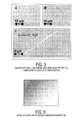
- FIG. 2B shows the various prototypes of optical components according to the invention.
- the thickness of the molecule given by the device is 1.7 nm, which closely matches the theoretical diameter of the molecule, which is 2 nm.
- Part b shows a new image of the same molecule obtained using the same microscope after the study with the AFM.
- the nanometric defects introduced by AFM scanning draw a clearly visible square. Without previous optical marking, it is impossible to locate a given object as small as this molecule on a reasonably sized sample (larger than one square millimetre).
- FIG. 4 shows an example of application for the production of a biochip with membrane proteins, designed for observation in the air for the purpose of analysing a mix.
- the component ( 30 ) has a silicon substrate ( 31 ) and a layer with an index of 1.34 as well as selective affinity layers ( 34 ) consisting of studs with a thickness of 5 nm and irregular contours.
- the index layer is a silica aerogel and has a thickness of 102.5 nm and a real index of 1.34.
- the affinity layer ( 34 ) covering the surface is placed on an index layer ( 33 ) which can be formed from a highly hydrophobic self-assembled monolayer ( FIG. 4B ), a hydrophilic film ( FIG. 4C ), a cushion of polymer ( FIG. 4D ) or hybrid molecules grafted onto the surface ( FIG. 4E ).
- the studs have diameters of several dozen microns. These are discs made up of a membrane bilayer with a thickness of 5 nm which supports different receptors ( 35 ) for each stud, which are then capable of selectively quenching a ligand ( 36 ) present in an environment to be analysed.
- the biological material is made up of a lipid bilayer having membrane receptors ( 35 ) designed to sense a ligand ( 36 ). In contact with the environment, the studs each capture the complementary species of the receptor that they support.
- Each stud captures a low or very low number of objects, which can be protein or peptide partners such as antibodies or hormones.
- the reading is carried out after rinsing by interferential contrast.
- Each object captured (nanometric) is displayed as a shiny point on a slightly luminous background. The objects can be easily counted.
- the analysis method according to the invention is particularly advantageous compared with current fluorescence or ellipsometry techniques, since the signal it uses at one point of the image is generated by a very small surface around the captured object, typically the square of the lateral resolution of the observation system which corresponds to the smallest observable surface, or clearly less than one square micron, unlike fluorescence or ellipsometry techniques which use a signal generated by a much larger spot of light, larger than 100 square microns.
- the signal-to-noise ratio improves considerably when implementing the analysis method according to the invention.
- the present invention therefore makes it possible to recognise the individual objects captured while the other techniques mentioned require the presence of a large number of identical objects in order to detect them. This constitutes an enormous advantage since the objects searched for in certain environments are very rare. Our technique is therefore preferable in every situation where the captured objects are of nanometric dimensions or are attached to objects of nanometric dimensions.
- FIG. 4F shows a supported bilayer observed in the air.
- Image 5 which shows a supported bilayer observed in water, was obtained by immersion and in interferential contrast with support no. 15 ( FIG. 2B ).
- the component ( 30 ) has a silicon substrate ( 31 ) and a layer with an index of 1.74 as well as selective affinity layers ( 34 ) consisting of studs with a thickness of 5 nm and irregular contours.
- FIG. 6 shows images obtained using the analysis system according to the invention for DNA chips.
- the surface of the component has a matrix of different types of affinity areas. Each area corresponds to a different affinity layer, comprising specific biological material. Such a component is placed in contact with a biological sample to be analysed.
- Biochemical reactions take place between this sample and the biological material fixed to the various affinity areas of the component.
- the areas that brought about a biomolecular interaction have excess thicknesses of nanometric order and specific optical characteristics, in which observation using the system according to the invention leads to direct visualisation that makes it possible to deduce the biological nature of the sample.
- Diagram 6 A summarises the experiments conducted on the optical components according to the invention.
- the deposited DNA molecules are products of PCR with a length of 1000 base pairs.
- the biochips are prepared and revealed by means of a confidential method perfected by the Inserm U533 unit directed by Jean Léger.
- Image 6 C shows that in this step it is possible to tell the deposits of solutions of PCR products from buffer deposits. A quick check of the spots makes it possible to ensure that they all have the same appearance, the same size and that they are homogeneous. Insufficiencies in the rinsing process leave residue that our technique can detect and qualify (manufacturing process control).
- BSA bovine serum albumin
- the intensities and colours are thresholded so that the studs that capture DNA strands, or positive studs, appear covered with shiny points while the studs that do not capture anything, or negative studs, no longer appear ( FIG. 6D ).
- FIG. 6E The deposits observed by our technique correspond to fluorescent deposits in microscopy (Image 6 F) and under the scanner. And yet, this fluorescence is the consequence of hybridisation. That observed by our technique is therefore also the result of hybridisation.
- the fluorescence signals after reading under the scanner are quantified.
- the signals for Cy3 and Cy5 are added up.
- the deposited fragments have a standard size of 1000 pb, but these 3 solutions contain smaller fragments: R056X01A01->500 pb, R056X01E05->300 pb, R056X01M05->500 pb.
- Sarfus makes it possible to view hybridisations with probes greater than 600 pb but not hybridisations with smaller probes.
- Image 6 I shows that the differentiation between the stud and its environment is very large, that the defects of the stud and of the environment are clearly visible. This technique is therefore highly effective for checking manufacturing and incubation processes.
- Image 6 J shows that the appearance of the hybridised stud is clearly different from that of the non-hybridised stud, the quenched DNA resulting in an excess thickness and introducing additional roughness.
- This technique of reading chips without marking has a considerable advantage over fluorescence techniques in that the signal used is refractive in origin and therefore stable in time under lighting, unlike the fluorescence signal, which changes with the lighting time.
- the technique also has the advantage of being compatible with very high-density chips, the minimum surface of a stud being around or less than one square micron.
- FIG. 7A shows two-dimensional protein crystals.
- the observed area has a length of 100 microns.
- FIG. 7B shows the thin three-dimensional crystals of identical proteins obtained at a later stage.
- the image is 200 microns long.
- the surface of the component has been modified to make it hydrophilic, allowing the bovine serum albumin (BSA) present in the solution to deposit and crystallise when the solvent evaporates.
- BSA bovine serum albumin
- FIG. 7C shows 2D polymer crystals (Polyethylene Glycol 4000). The observed areas are respectively 100 microns and 200 microns long. The dendrites have a thickness of approximately 4 nm.
- FIG. 7D shows the three-dimensional view of the crystallisation of this same polymer at room temperature.
- the images are 100 microns long. The formation of these dendrites on the surface is quick (around one micron per minute). This sequence of images shows the possibility of observing the kinetics of crystallisation at room temperature, which is inaccessible using other techniques.
- the large side of the six images in FIG. 8 is 200 microns.
- the first five are obtained dry between a crossed polariser and an analyser using component no. 7 (according to FIG. 2B ).
- the component used for the sixth image (bottom right) is a simple silicon support covered with a film of a solution in water with an approximate thickness of 100 nm, which can be checked with a device for checking segregation pressure, such as provided by Moldover and Cahn (Physical Review Letters, 1986).
- a device for checking segregation pressure such as provided by Moldover and Cahn (Physical Review Letters, 1986).
- the observation is conducted using differential interference contrast.
- the samples are obtained from a solution of Beta-lactoglobulin (a milk protein) in water, used as it is (sixth image) or deposited on a surface activated by UV irradiation under oxygen (the other five images). This solution forms a gel whose growth is governed by the pH of the solution, checked during the experiment.
- This example illustrates the possibility of following up, inspecting and controlling the processes of gelling and, more generally, of aggregation and crystallisation of proteins or other products, which is particularly advantageous in the agri-food sector, in particular for improving processes and checking production (texture of ice-cream, cheese, cream, yoghourt, etc.). It is also useful in the cosmetic sector, where a control of textures is equally important.
- the observation method in this case is an alternative to confocal microscopy.
- the images show the structures formed at different times by the Beta-lactoglobulin in a solution (image 6 in FIG. 8 ) or after evaporation of a solution (other images in FIG. 8 ).
- FIG. 9A shows an image obtained with an example of the analysis system for studying and inspecting nanotubes. This image was obtained after CVD synthesis and shows an isolated multi-walled nanotube with the catalytic nanoparticle at one end.
- the analysis method according to the invention makes it possible to categorise all these different types of nanotubes.
- CVD chemical vapour deposition
- CVD chemical vapour deposition
- Another method of manufacturing nanotubes is laser ablation. Our technique makes it possible to view the result of this ablation on site.
- Another manufacturing method is the electric are method. This method is characterised by the great dispersity of the manufactured nanotubes. Our technique makes it possible to view and, at the same time, to sort certain nanotubes using an AFM.
- the top surface must be free for micromanipulation.
- a “rear surface” component on an inverse microscope.
- This component has the following characteristics: it consists of a floated glass substrate with a thickness of 1 millimetre, covered on one side only with a layer of chromium with a thickness of 5.3 nanometers and a layer of chromium dioxide (CrO 2 ) with a thickness of 6 nanometers.
- the substrate is used in reflection on the covered surface and is attacked with light by the other surface.
- the useful surface is therefore observed through the glass.
- the surface can be used with its natural properties (high energy for direct deposition with strong anchoring of the tubes on the surface, for the purpose of inspection, counting or marking, for spectroscopic studies for example) or covered with a thin film of an amorphous polymer such as polydimethylsiloxane or even covered with a layer grafted by a chemical operation on the surface in vapour phase (for deposition by combing using a solution for micromanipulation operations).
- FIG. 9B shows the detection of carbon nanotubes with rare shapes among interesting objects.
- This image which has a length of 200 microns, was obtained by immersion and in interference contrast using support no. 16 (of FIG. 2B ). It was then modified by silanisation using octadecyltrichlorosilane in toluene after UV+02 activation of the surface.
- the nanotubes shown in FIG. 9B have been previously stabilised in an aqueous solution with SDS (sodium dodecyl sulphate) surface active agents.
- SDS sodium dodecyl sulphate
- the interaction between the surface active agents and the silane layer is favourable for dispersed deposition of well-separated nanotubes.
- FIG. 10 shows an image with a length of 159 microns, which was obtained by immersion and by interference contrast with support no. 16 (of FIG. 2B ), used with its natural surface properties. Indeed, it has considerable affinity for bacteria.
- This component associated with an interference contrast observation, makes it possible to follow up the growth of a bacterial population which develops on the surface.
- the polymerised networks woven by the bacteria on the surface are not visible in this image due to the contrast settings, given by the choice of component, but can be visualised using component no. 13 (of FIG. 2B ).
- the bacteria are Escherichia coli .
- the method allows the detection of bacterial growth.
- Components having specific affinity for bacteria allow excellent environmental control, in particular in the food sector.
- FIG. 11A shows a differential contrast device according to the invention.
- a device for imaging a sample (E) in interference contrast by reflection comprises a light source (S); a lens (O); an imagery device of the light source next to the pupil of the lens (L); at least one polarising element (P, A); a polarisation separation element (W); a semi-transparent mirror (M).
- colour filters can, in turn, be dichroic.
- a compensator element C
- LT tube lens
- OC eyepieces
- CAM camera
- L/4 lambda/4 retardation plate
- LR another retardation plate
- COMP compensator
- the element W introduces a lateral shift between two linear polarisations in a direction located at 45° with regard to the X and Y axes. This is, for example, a Wollaston biprism.
- the camera or the ocular device are placed after (M).
- the possible tube lens is placed between (M) and (C) or (OE).
- FIG. 11B shows different configurations of the differential contrast device.
- a system for observing a sample (E) between crossed polarisers with no interference contrast is less restricting than the system described in the preceding example.
- FIG. 12 shows an imagery-free measurement system between crossed polarisers.
- This system is a monosensor (the functional surface is homogeneous; there is no imagery).
- FIG. 13A shows a rectangular area of the surface of the component with a length of 200 microns.
- the component is obtained by modifying the surface of component no. 7 (of FIG. 2B ) using caesium hydroxide.
- the sample thus formed is subjected to a succession of alternating thermal shocks at ⁇ 15° C. and +30° C.
- the cell ruptures and its chromatin is extracted.
- Image 13 A shows, on the left-hand side, the cellular residue.
- the sample is kept in a humid atmosphere.
- a part of the chromatin emerges gradually to the surface (towards the right) while another part remains packed and seems to form condensed chromosomes (to the left of the residue).
- the stretched part corresponds to an unfolded chromosome with a thickness of around 30 nm.
- the two strands of the chromosome are clearly visible and are bound by a bridge (white stain shared by the strands towards the right of the image), which is clearly pronounced of a centromere.
- FIG. 13B shows the 100-micron long side of the preceding image, taken on the same system with greater magnification. This image shows the still-packed chromosomes more clearly.
- the shiny object located at the top has low-contrast coloured bands which allow it, in principle, to be identified.
- FIG. 13C shows the two images that have a length of 100 microns and are obtained in the same conditions as above. They illustrate the possibility of probing the interactions between partially unpacked DNA molecules (diameters between 10 and 30 nm according to brilliance) and varied biological objects (not identified here).
- FIG. 13D show two unpacked DNA molecules obtained following the same method using a highly diluted solution of human saliva.
- the method allows genetic diagnoses to be made for the purpose of diagnosis or analysis, for example for sequencing. It has the enormous advantage of economising the PCR amplification and of allowing savings in terms of fluorescent markers, of being very easy to use and of providing much more accurate information: it is not only possible to find out what association takes place, but also where it takes place along the strand. For these reasons, the technique is an advantageous alternative to the FISH techniques (developed, for example, at the Pasteur Institute by Aaron Bensimon).
- Image 14 A has a length of 200 microns. The observation is made in interferential contrast.
- the component is component no. 7 (of FIG. 2B ). Its surface is made hyper-hydrophilic by exposure to UV light coming from a discharge lamp with a strong component with a wavelength of 240 nanometers.
- a highly diluted solution of human saliva is diluted in a glass of water (at an approximate ratio of 1 to 10,000) and one drop of this solution is deposited on the surface of the component.
- the eukaryote cells contained in the solution become strongly adhered to this surface and the cellular membrane, a bilayer in which the outer parts are hydrophilic, presses against the surface (clear disc) around the nucleus (coloured mass).
- the evaporation of the water then increases the ionic force of the intracellular fluid and opens the walls of the nuclear membrane.
- the chromatin (coloured mass) is then extracted from the nucleus to take up the space between the two bilayers, still filled with fluid as can be seen by the brightening of the disc at its bottom right-hand side.
- the method described in this example therefore enables all the operations that involve the ligands of these accessible objects. These ligands can directly detect or be themselves equipped with steric or fluorescent markers. The method allows the addressed receptors to be identified and located.
- the two images in FIG. 14B show analogous cells obtained in the same conditions in an earlier stage (image on the left) and in a later stage (image on the right) of the process.
- the sample corresponding to the image on the right was subjected to successive thermal shocks at ⁇ 20° C. and +20° C. in a humid atmosphere, leading the chromatin to unpack on the surface.
- Image 14 C obtained with the same settings, the same procedure and the same components as the preceding image, illustrates the usefulness of these observations for studying cellular mechanisms: in this case a cell in the anaphase stage of mitosis.
- the two nuclei can be clearly seen (large objects on the left and right of the disc) and the masses of chromosomes (spread out at the ends of the equatorial plane). At the centre, traces of sleeves. The method allows the study of cellular mechanisms and the detection of functional or structural anomalies.
- the present example is dedicated to the observation of a DNA solution immersed for the purpose of analysis and diagnosis.
- Image 15 A corresponding to an observed window with a total length of 159 microns, is obtained by interference contrast and by immersion.
- the solution is a rat brain DNA solution and the component is no. 15 ( FIG. 2B ).
- association in a solution and visualisation by an adsorbent solution is an example of the diagnosis method that can be implemented using the component.
- Image 15 B of the same system is obtained after several hours of incubation and shows the associations of surface active agents contained in the initial solution with certain regions of the adsorbed molecules. Brownian diffusion mechanisms govern the kinetics of these associations, which can be speeded up by mechanical agitation or a hydrodynamic flow.
- This example shows the possibility of performing tests based on physical-chemical associations in the interface between the component and a solution or solutions.
- the present example shows the application of the method according to the invention to the analysis of chromosomes.
- the images of FIG. 16 have a length of 100 microns.
- the image on the left was obtained by observation of the sample between a crossed polariser and analyser, and the image on the left is obtained by Nomarski's differential interference contrast.
- the two main objects visible in FIG. 16 are unfolded chromosomes probably taken from a cell in a pre-metaphase stage of mitosis.
- One advantage of the analysis method according to the invention is that it does not require a specific mitotic phase to be blocked, since the objects extracted from the various cells are instantly recognised.
- Direct analysis for example for the purpose of diagnosis, is made possible by observation of the coloured bands that appear without marking and therefore without destruction of the objects.
- Another advantage is that a small number of cells is sufficient for implementing the observation.
- the chromosome is a human chromosome.
- the lighting lamp is a xenon lamp.
- the image on the left ( FIG. 16 ) clearly shows the coloured bands and the image on the right shows the two strands of the chromosome and the centromere at the level of the fracture in the shape of the object.
- the image of FIG. 17 obtained by differential interference contrast, has a length of 15 microns and shows a population of colloidal gold balls, most of which have a diameter of 20 nanometers, deposited on component no. 7 ( FIG. 2B ) from a solution.
- the component is made hydrophobic by depositing HDMS in vapour phase, which allows good dispersion of the deposited suspension by the movement of a drop on the surface with the help of a Pasteur pipette, a technique similar to combing which we practice.
- the speed of the drop parallel to the support is of the order of 1 millimetre per second.
- FIG. 18A which have respective lengths of 200 microns (left) and 100 microns (right), show on component no. 7 (according to FIG. 2B ) (on the left) and no. 7 modified by silanisation (on the right) the impact of the affinity of the surface on the structure of cationic surface active monolayers (SDS at 0.1%).
- the surface active agents are deposited by evaporation from a solution highly diluted in distilled water.
- the layers are regular but either have holes in them (monolayer in the top left) or not (trilayer in the bottom right), suggesting chaotic positioning of the molecules, as in a liquid state.
- image 18 B on the left taken in the same conditions, shows the crystalline structures obtained on the hydrophilic component.
- Image 19 which has a length of 153 microns, shows a bilayer of phospholipids on a component no. 16 ( FIG. 2B ) after UV irradiation under oxygen.
- the bilayer was obtained by depositing a very small amount of a solution of DPCC liposomes, a reference phospholipid.
- the deposition is carried out by direct contact (both solid and liquid) between a manual spotter with a diameter of 100 microns dipped in the solution and the component.
- the observation is then carried out in the water by interference contrast.
- the observation shows the presence of a very regular bilayer (except at the top left) which is very stable in water.
- a bilayer can constitute a spot of a protein biochip.
- the deposition technique is also compatible with the use of automatic spotters, and the bilayer can accommodate all kinds of receptors, previously introduced by mixing in the DPPC solution, the receptors then becoming integrated in the liposome bilayers.
- a different solution can be used for each spot, containing receptors determined after using the biochip.
- Liposomes are vesicles (sacs) in which the membrane is a bilayer of phospholipids. They are used for targeting active products in the cosmetic and pharmaceutical sectors, the sacs opening when in contact with the target.
- the present invention allows this study and this inspection.
- the surface properties of the component must then reproduce those of the target.
- Image 20 A has a length of 159 microns. The observation is made by interference contrast in immersion.
- the liposomes of unknown nature are objects from the cosmetics industry.
- the liposomes are spontaneously adsorbed on the component in which the surface is very homogeneous in the form of semi-liposomes, that is to say of hemispheres resting on the surface.
- the angle of contact of the objects on the surface is constant and very close to 90°.
- the shiny points correspond to objects with a diameter of 50 nanometers.
- Enlargement of image 20 B by a factor of around 10 shows how the size of the liposomes affects their appearance.
- the balls with a diameter barely smaller than 100 nanometers appear as very luminous stains with an apparent diameter that is comparable with the resolution of the microscope used, which is to say around 300 nanometers.
- Another population of much smaller objects, with an approximate diameter of 10 nanometers, takes on the appearance of stains with a diameter that is comparable with that of the preceding stains, but with a considerably lower luminosity.
- the suspension is therefore essentially bidisperse.
- the component allows a functional link to be established between the size of the objects and their appearance (calibration), and then to follow-up changes in the distribution of objects in the solution, with the storage conditions and duration, for example.
- This application is very advantageous since it allows direct, easy to implement characterisation of objects observed individually, while the available techniques, based on the distribution of light (scatterometry) only provide access to mean quantities for the entire population.
- the thickness e can be adjusted by means of the following device.
- a mechanical or piezoelectric device or the variation of the level of the Langmuir layer making it possible to place the optical component in a position h with a precision of the order of one nanometer.
- the thickness e of the film results from a balance between segregation pressure and gravity.
- An adjustment of h makes it possible to adjust e with a precision of the order of several nanometers, such as to obtain maximum contrast.
Landscapes
- Physics & Mathematics (AREA)
- Health & Medical Sciences (AREA)
- Life Sciences & Earth Sciences (AREA)
- Chemical & Material Sciences (AREA)
- Analytical Chemistry (AREA)
- Biochemistry (AREA)
- General Health & Medical Sciences (AREA)
- General Physics & Mathematics (AREA)
- Immunology (AREA)
- Pathology (AREA)
- Investigating Or Analysing Materials By Optical Means (AREA)
- Investigating, Analyzing Materials By Fluorescence Or Luminescence (AREA)
Applications Claiming Priority (3)
| Application Number | Priority Date | Filing Date | Title |
|---|---|---|---|
| FR0407517A FR2872910B1 (fr) | 2004-07-07 | 2004-07-07 | Composant optique pour l'observation d'un echantillon nanometrique, systeme comprenant un tel composant, procede d'analyse mettant en oeuvre ce composant, et leurs applications |
| FR0407517 | 2004-07-07 | ||
| PCT/FR2005/001746 WO2006013287A1 (fr) | 2004-07-07 | 2005-07-06 | Composant optique pour l'observation d'un echantillon nanometrique, systeme comprenant un tel composant, procede d'analyse mettant en oeuvre ce composant, et leurs applications |
Publications (2)
| Publication Number | Publication Date |
|---|---|
| US20100062422A1 US20100062422A1 (en) | 2010-03-11 |
| US8088615B2 true US8088615B2 (en) | 2012-01-03 |
Family
ID=34948199
Family Applications (1)
| Application Number | Title | Priority Date | Filing Date |
|---|---|---|---|
| US11/631,846 Expired - Fee Related US8088615B2 (en) | 2004-07-07 | 2005-07-06 | Optical component for observing a nanometric sample, system comprising same, analysis method using same, and uses thereof |
Country Status (6)
| Country | Link |
|---|---|
| US (1) | US8088615B2 (fr) |
| EP (1) | EP1779092A1 (fr) |
| JP (1) | JP2008506098A (fr) |
| CN (1) | CN101031789A (fr) |
| FR (1) | FR2872910B1 (fr) |
| WO (1) | WO2006013287A1 (fr) |
Cited By (4)
| Publication number | Priority date | Publication date | Assignee | Title |
|---|---|---|---|---|
| US20080142735A1 (en) * | 2006-10-31 | 2008-06-19 | Fei Company | Charged-particle-beam processing using a cluster source |
| US20130055819A1 (en) * | 2011-09-03 | 2013-03-07 | John Yan | Unpowered, Wireless Pressure Sensor for Point-of-Care Glaucoma Diagnosis |
| US20150185457A1 (en) * | 2012-07-26 | 2015-07-02 | Centre National De La Recherche Scientifique | Optical Methods for Observing Samples and for Detecting or Metering Chemical or Biological Species |
| US11498156B2 (en) * | 2014-07-03 | 2022-11-15 | Nippon Steel Corporation | Laser processing apparatus |
Families Citing this family (33)
| Publication number | Priority date | Publication date | Assignee | Title |
|---|---|---|---|---|
| US7461002B2 (en) | 2001-04-13 | 2008-12-02 | Dolby Laboratories Licensing Corporation | Method for time aligning audio signals using characterizations based on auditory events |
| US7283954B2 (en) | 2001-04-13 | 2007-10-16 | Dolby Laboratories Licensing Corporation | Comparing audio using characterizations based on auditory events |
| US7508947B2 (en) | 2004-08-03 | 2009-03-24 | Dolby Laboratories Licensing Corporation | Method for combining audio signals using auditory scene analysis |
| FR2908414B1 (fr) * | 2006-11-13 | 2012-01-20 | Centre Nat Rech Scient | Immobilisation de proteines membranaires sur un support par l'intermediaire d'une molecule amphiphile |
| US7822273B1 (en) * | 2007-05-16 | 2010-10-26 | Gianni Arcaini | Method and apparatus for automatic corrosion detection via video capture |
| KR100911626B1 (ko) | 2007-07-13 | 2009-08-12 | 서강대학교산학협력단 | 바이오 센서 측정 장치 |
| CN101403742B (zh) * | 2008-10-29 | 2012-05-23 | 东南大学 | 利用光电镊对微纳米生物粒子进行介电表征的方法 |
| US8415611B2 (en) * | 2009-11-19 | 2013-04-09 | Seiko Epson Corporation | Sensor chip, sensor cartridge, and analysis apparatus |
| CN105734170A (zh) * | 2010-04-23 | 2016-07-06 | 基因组影像公司 | 通过由分子梳检测基因组和感染性病毒dna的病毒感染的诊断 |
| JP5457262B2 (ja) * | 2010-04-23 | 2014-04-02 | 浜松ホトニクス株式会社 | 膜電位変化検出装置および膜電位変化検出方法 |
| CN102243422B (zh) * | 2011-07-01 | 2013-06-26 | 苏州佳世达光电有限公司 | 投影机及其灰尘过滤器的清洁装置及对其进行清洁的方法 |
| CN103424365B (zh) * | 2012-05-25 | 2016-02-24 | 博奥生物集团有限公司 | 一种微载体生物芯片及其应用 |
| CN102895930B (zh) * | 2012-11-15 | 2014-04-09 | 哈尔滨工业大学 | 利用指状微电极制备磷脂纳米/微米管的方法 |
| FR3012131B1 (fr) * | 2013-10-18 | 2018-01-19 | Centre National De La Recherche Scientifique | Supports amplificateurs de contraste pour l'observation d'un echantillon, leur procedes de fabrication et leurs utilisations |
| CN104808326B (zh) * | 2014-01-25 | 2017-10-24 | 清华大学 | 一种光学显微镜的辅助装置 |
| CN104808325B (zh) * | 2014-01-25 | 2017-10-24 | 清华大学 | 一种通过光学显微镜观测纳米结构的方法 |
| FR3020138B1 (fr) * | 2014-04-16 | 2016-05-20 | Dominique Ausserre | Appareil et procede d'observation d'une couche a la surface d'un liquide. |
| CN104697946B (zh) * | 2015-02-04 | 2018-05-08 | 北京大学 | 一种衬底上碳纳米管水平阵列密度的快速光学表征方法 |
| CN105785433A (zh) * | 2016-02-04 | 2016-07-20 | 中国科学院电子学研究所 | Mems电化学地震检波器敏感电极芯片及其制造方法 |
| CN107402184B (zh) * | 2016-05-20 | 2020-01-03 | 清华大学 | 一种测量纳米结构表面电荷分布的方法 |
| CN107402440B (zh) * | 2016-05-20 | 2020-01-07 | 清华大学 | 一种观测纳米结构表面电荷分布的方法 |
| CN108020573B (zh) * | 2016-10-31 | 2019-12-17 | 清华大学 | 区分碳纳米管类型的方法 |
| CN107037001A (zh) * | 2017-06-15 | 2017-08-11 | 中国科学院半导体研究所 | 一种基于近红外光谱技术的玉米单倍体籽粒鉴别方法 |
| CN107356571A (zh) * | 2017-06-27 | 2017-11-17 | 暨南大学 | 一种测定表面电荷的方法 |
| US10660523B2 (en) | 2017-07-07 | 2020-05-26 | Hideo Ando | Light-source unit, measurement apparatus, near-infrared microscopic apparatus, optical detection method, imaging method, calculation method, functional bio-related substance, state management method, and manufacturing method |
| CN109932377A (zh) * | 2017-12-15 | 2019-06-25 | Tcl集团股份有限公司 | 一种量子点表面配体覆盖率的测定方法 |
| EP3844677A1 (fr) * | 2018-08-31 | 2021-07-07 | Life Technologies Corporation | Contrôle de qualité par l'image pour pcr basée sur une matrice |
| EP3696534A1 (fr) * | 2019-02-14 | 2020-08-19 | SmartDyeLivery GmbH | Procédé pour déterminer les propriétés physicochimiques de systèmes nanométriques (nss) |
| WO2021046759A1 (fr) * | 2019-09-11 | 2021-03-18 | Covestro Deutschland Ag | Appareil, système et procédé de contrôle de qualité de pastilles de polymère et procédé de commande de chaîne de production pour la production de pastilles de polymère |
| CN110927107B (zh) * | 2019-12-02 | 2021-07-23 | 四川大学 | 照射双棱镜单侧棱面实现测量材质折射率的方法 |
| CN110927105B (zh) * | 2019-12-02 | 2021-07-20 | 四川大学 | 一种双棱镜材质折射率的测量方法 |
| CN110927108B (zh) * | 2019-12-02 | 2021-07-20 | 四川大学 | 照射双棱镜的棱和底面测量材质折射率的方法 |
| CN111175251B (zh) * | 2020-01-15 | 2021-08-03 | 四川大学 | 照射双棱镜的棱面和底面测量材质折射率的方法 |
Citations (13)
| Publication number | Priority date | Publication date | Assignee | Title |
|---|---|---|---|---|
| US5639671A (en) * | 1989-09-18 | 1997-06-17 | Biostar, Inc. | Methods for optimizing of an optical assay device |
| US5962114A (en) * | 1993-12-21 | 1999-10-05 | 3M Innovative Properties Company | Polarizing beam-splitting optical component |
| US6034775A (en) * | 1996-10-09 | 2000-03-07 | Symyx Technologies, Inc. | Optical systems and methods for rapid screening of libraries of different materials |
| US6312691B1 (en) * | 1996-01-26 | 2001-11-06 | Jeffrey L. Browning | Lymphotoxin-α/β complexes and anti-lympotoxin-β receptor antibodies as anti-tumor agents |
| US6493423B1 (en) * | 1999-12-24 | 2002-12-10 | Koninklijke Philips Electronics N.V. | Method of generating extremely short-wave radiation, method of manufacturing a device by means of said radiation, extremely short-wave radiation source unit and lithographic projection apparatus provided with such a radiation source unit |
| US6697194B2 (en) * | 2000-12-15 | 2004-02-24 | Carl Zeiss Smt Ag | Antireflection coating for ultraviolet light at large angles of incidence |
| US6710875B1 (en) * | 1997-11-07 | 2004-03-23 | Lucid, Inc. | Imaging system using polarization effects to enhance image quality |
| US6718053B1 (en) * | 1996-11-27 | 2004-04-06 | Chromavision Medical Systems, Inc. | Method and apparatus for automated image analysis of biological specimens |
| US6853455B1 (en) * | 1998-04-03 | 2005-02-08 | Bio-Rad Laboratories, Inc. | Apparatus and methods for fourier spectral analysis in a scanning spot microscope |
| US6934068B2 (en) * | 2003-02-10 | 2005-08-23 | Lake Shore Cryotronics, Inc. | Magnetic field and electrical current visualization system |
| US7209232B2 (en) * | 2000-12-18 | 2007-04-24 | Centre National De La Recherche Scientifique (Cnrs) | Device for ellipsometric two-dimensional display of a sample, display method and ellipsometric measurement method with spatial resolution |
| US7258838B2 (en) * | 1999-06-22 | 2007-08-21 | President And Fellows Of Harvard College | Solid state molecular probe device |
| US7265845B2 (en) * | 2003-01-27 | 2007-09-04 | Lake Shore Cryotronics, Inc. | Surface corrugation enhanced magneto-optical indicator film |
Family Cites Families (4)
| Publication number | Priority date | Publication date | Assignee | Title |
|---|---|---|---|---|
| US5268305A (en) * | 1989-06-15 | 1993-12-07 | Biocircuits Corporation | Multi-optical detection system |
| GB9406142D0 (en) * | 1994-03-28 | 1994-05-18 | British Tech Group | A sensor |
| SE9504417D0 (sv) * | 1995-12-11 | 1995-12-11 | Siemens Elema Ab | Metod för att bestämma koncentrationen av en specifik gas och en analysapparat |
| FR2841339B1 (fr) * | 2002-06-19 | 2004-09-10 | Centre Nat Rech Scient | Supports anti-reflechissants et supports amplificateurs de contraste pour la lumiere polarisee en reflexion |
-
2004
- 2004-07-07 FR FR0407517A patent/FR2872910B1/fr not_active Expired - Lifetime
-
2005
- 2005-07-06 EP EP05788741A patent/EP1779092A1/fr not_active Withdrawn
- 2005-07-06 US US11/631,846 patent/US8088615B2/en not_active Expired - Fee Related
- 2005-07-06 WO PCT/FR2005/001746 patent/WO2006013287A1/fr active Application Filing
- 2005-07-06 JP JP2007519841A patent/JP2008506098A/ja active Pending
- 2005-07-06 CN CNA2005800299597A patent/CN101031789A/zh active Pending
Patent Citations (13)
| Publication number | Priority date | Publication date | Assignee | Title |
|---|---|---|---|---|
| US5639671A (en) * | 1989-09-18 | 1997-06-17 | Biostar, Inc. | Methods for optimizing of an optical assay device |
| US5962114A (en) * | 1993-12-21 | 1999-10-05 | 3M Innovative Properties Company | Polarizing beam-splitting optical component |
| US6312691B1 (en) * | 1996-01-26 | 2001-11-06 | Jeffrey L. Browning | Lymphotoxin-α/β complexes and anti-lympotoxin-β receptor antibodies as anti-tumor agents |
| US6034775A (en) * | 1996-10-09 | 2000-03-07 | Symyx Technologies, Inc. | Optical systems and methods for rapid screening of libraries of different materials |
| US6718053B1 (en) * | 1996-11-27 | 2004-04-06 | Chromavision Medical Systems, Inc. | Method and apparatus for automated image analysis of biological specimens |
| US6710875B1 (en) * | 1997-11-07 | 2004-03-23 | Lucid, Inc. | Imaging system using polarization effects to enhance image quality |
| US6853455B1 (en) * | 1998-04-03 | 2005-02-08 | Bio-Rad Laboratories, Inc. | Apparatus and methods for fourier spectral analysis in a scanning spot microscope |
| US7258838B2 (en) * | 1999-06-22 | 2007-08-21 | President And Fellows Of Harvard College | Solid state molecular probe device |
| US6493423B1 (en) * | 1999-12-24 | 2002-12-10 | Koninklijke Philips Electronics N.V. | Method of generating extremely short-wave radiation, method of manufacturing a device by means of said radiation, extremely short-wave radiation source unit and lithographic projection apparatus provided with such a radiation source unit |
| US6697194B2 (en) * | 2000-12-15 | 2004-02-24 | Carl Zeiss Smt Ag | Antireflection coating for ultraviolet light at large angles of incidence |
| US7209232B2 (en) * | 2000-12-18 | 2007-04-24 | Centre National De La Recherche Scientifique (Cnrs) | Device for ellipsometric two-dimensional display of a sample, display method and ellipsometric measurement method with spatial resolution |
| US7265845B2 (en) * | 2003-01-27 | 2007-09-04 | Lake Shore Cryotronics, Inc. | Surface corrugation enhanced magneto-optical indicator film |
| US6934068B2 (en) * | 2003-02-10 | 2005-08-23 | Lake Shore Cryotronics, Inc. | Magnetic field and electrical current visualization system |
Cited By (8)
| Publication number | Priority date | Publication date | Assignee | Title |
|---|---|---|---|---|
| US20080142735A1 (en) * | 2006-10-31 | 2008-06-19 | Fei Company | Charged-particle-beam processing using a cluster source |
| US8835880B2 (en) * | 2006-10-31 | 2014-09-16 | Fei Company | Charged particle-beam processing using a cluster source |
| US20150079796A1 (en) * | 2006-10-31 | 2015-03-19 | Fei Company | Charged-Particle-Beam Processing Using a Cluster Source |
| US20130055819A1 (en) * | 2011-09-03 | 2013-03-07 | John Yan | Unpowered, Wireless Pressure Sensor for Point-of-Care Glaucoma Diagnosis |
| US8850895B2 (en) * | 2011-09-03 | 2014-10-07 | John Yan | Unpowered, wireless pressure sensor for point-of-care glaucoma diagnosis |
| US20150185457A1 (en) * | 2012-07-26 | 2015-07-02 | Centre National De La Recherche Scientifique | Optical Methods for Observing Samples and for Detecting or Metering Chemical or Biological Species |
| US10241311B2 (en) * | 2012-07-26 | 2019-03-26 | Centre National De La Recherche Scientifique | Optical methods for observing samples and for detecting or metering chemical or biological species |
| US11498156B2 (en) * | 2014-07-03 | 2022-11-15 | Nippon Steel Corporation | Laser processing apparatus |
Also Published As
| Publication number | Publication date |
|---|---|
| FR2872910A1 (fr) | 2006-01-13 |
| US20100062422A1 (en) | 2010-03-11 |
| JP2008506098A (ja) | 2008-02-28 |
| WO2006013287A1 (fr) | 2006-02-09 |
| FR2872910B1 (fr) | 2006-10-13 |
| EP1779092A1 (fr) | 2007-05-02 |
| CN101031789A (zh) | 2007-09-05 |
Similar Documents
| Publication | Publication Date | Title |
|---|---|---|
| US8088615B2 (en) | Optical component for observing a nanometric sample, system comprising same, analysis method using same, and uses thereof | |
| JP2008506098A5 (fr) | ||
| US9547018B2 (en) | Analyte detection using liquid crystals | |
| JP4209471B2 (ja) | プラズモン共鳴粒子、方法、および装置 | |
| US8003408B2 (en) | Modification of metal nanoparticles for improved analyte detection by surface enhanced Raman spectroscopy (SERS) | |
| Bauer et al. | Resonant nanocluster technology—from optical coding and high quality security features to biochips | |
| García-Sáez et al. | Surface analysis of membrane dynamics | |
| US20120208174A1 (en) | Plasmonic System for Detecting Binding of Biological Molecules | |
| Zhang et al. | A photonic crystal hydrogel suspension array for the capture of blood cells from whole blood | |
| KR20160138059A (ko) | 향상된 검정 감도를 위한 디지털 lspr | |
| US20080293590A1 (en) | Multianalyte assay method | |
| WO2003005013A1 (fr) | Puce a microreseau base sur la filtration | |
| CA2455427A1 (fr) | Detection sensible et rapide d'organismes pathogenes et de toxines a l'aide de lipides polymeres fluorescents | |
| AU771927B2 (en) | Multihued labels | |
| Gao et al. | Seeing the unseen: Imaging rotation in cells with designer anisotropic particles | |
| US8114602B2 (en) | Detection of molecular interactions | |
| US7824927B2 (en) | Analyte detection using an active assay | |
| Kotsev et al. | Refractive index of transparent nanoparticle films measured by surface plasmon microscopy | |
| Stamm et al. | Functionalization of ceramic liposomal nanoparticles, cerasomes, with antibodies | |
| Amorim | Development of a biosensor based on plastic antibodies for the isolation and detection of extracellular vesicles | |
| D'onofrio et al. | Controlling and measuring local composition and properties in lipid bilayer membranes | |
| Groves | Supported lipid bilayers as mimics for cell surfaces and as tools in biotechnology | |
| Iarossi | Fabrication and characterization of plasmonic nanopores for Raman detection of biomolecules | |
| Cavaleri | Printing methodologies for functional bioarrays | |
| Bauer et al. | Nano-clusters and Colloids in Bioanalysis |
Legal Events
| Date | Code | Title | Description |
|---|---|---|---|
| STCF | Information on status: patent grant |
Free format text: PATENTED CASE |
|
| FPAY | Fee payment |
Year of fee payment: 4 |
|
| FEPP | Fee payment procedure |
Free format text: MAINTENANCE FEE REMINDER MAILED (ORIGINAL EVENT CODE: REM.); ENTITY STATUS OF PATENT OWNER: LARGE ENTITY |
|
| LAPS | Lapse for failure to pay maintenance fees |
Free format text: PATENT EXPIRED FOR FAILURE TO PAY MAINTENANCE FEES (ORIGINAL EVENT CODE: EXP.); ENTITY STATUS OF PATENT OWNER: LARGE ENTITY |
|
| STCH | Information on status: patent discontinuation |
Free format text: PATENT EXPIRED DUE TO NONPAYMENT OF MAINTENANCE FEES UNDER 37 CFR 1.362 |
|
| FP | Expired due to failure to pay maintenance fee |
Effective date: 20200103 |