US8072278B2 - System and method for reducing power consumption of an oscillator - Google Patents
System and method for reducing power consumption of an oscillator Download PDFInfo
- Publication number
- US8072278B2 US8072278B2 US12/467,894 US46789409A US8072278B2 US 8072278 B2 US8072278 B2 US 8072278B2 US 46789409 A US46789409 A US 46789409A US 8072278 B2 US8072278 B2 US 8072278B2
- Authority
- US
- United States
- Prior art keywords
- oscillating signal
- crystal
- steady
- negative
- frequency
- Prior art date
- Legal status (The legal status is an assumption and is not a legal conclusion. Google has not performed a legal analysis and makes no representation as to the accuracy of the status listed.)
- Active, expires
Links
- 238000000034 method Methods 0.000 title claims description 31
- 239000013078 crystal Substances 0.000 claims abstract description 42
- 230000001939 inductive effect Effects 0.000 claims abstract description 40
- 238000004590 computer program Methods 0.000 claims description 3
- 230000000977 initiatory effect Effects 0.000 claims description 3
- 230000008878 coupling Effects 0.000 claims 3
- 238000010168 coupling process Methods 0.000 claims 3
- 238000005859 coupling reaction Methods 0.000 claims 3
- 230000001351 cycling effect Effects 0.000 claims 1
- 239000003990 capacitor Substances 0.000 abstract description 20
- 238000004891 communication Methods 0.000 description 23
- 238000010586 diagram Methods 0.000 description 23
- 230000004044 response Effects 0.000 description 14
- 230000003247 decreasing effect Effects 0.000 description 6
- 230000000694 effects Effects 0.000 description 6
- 230000008569 process Effects 0.000 description 6
- 238000012545 processing Methods 0.000 description 5
- 238000013461 design Methods 0.000 description 3
- 230000006870 function Effects 0.000 description 3
- 238000002955 isolation Methods 0.000 description 3
- 230000003287 optical effect Effects 0.000 description 2
- 230000010355 oscillation Effects 0.000 description 2
- 239000002245 particle Substances 0.000 description 2
- 230000006978 adaptation Effects 0.000 description 1
- 230000002411 adverse Effects 0.000 description 1
- 238000013459 approach Methods 0.000 description 1
- 230000000386 athletic effect Effects 0.000 description 1
- 230000005540 biological transmission Effects 0.000 description 1
- 230000001413 cellular effect Effects 0.000 description 1
- 230000008859 change Effects 0.000 description 1
- 238000005516 engineering process Methods 0.000 description 1
- 230000005669 field effect Effects 0.000 description 1
- 230000036541 health Effects 0.000 description 1
- 229910044991 metal oxide Inorganic materials 0.000 description 1
- 150000004706 metal oxides Chemical class 0.000 description 1
- 238000012986 modification Methods 0.000 description 1
- 230000004048 modification Effects 0.000 description 1
- 239000005022 packaging material Substances 0.000 description 1
- 230000000737 periodic effect Effects 0.000 description 1
- 239000004065 semiconductor Substances 0.000 description 1
- 230000011664 signaling Effects 0.000 description 1
- 230000007480 spreading Effects 0.000 description 1
Images


Classifications
-
- H—ELECTRICITY
- H03—ELECTRONIC CIRCUITRY
- H03B—GENERATION OF OSCILLATIONS, DIRECTLY OR BY FREQUENCY-CHANGING, BY CIRCUITS EMPLOYING ACTIVE ELEMENTS WHICH OPERATE IN A NON-SWITCHING MANNER; GENERATION OF NOISE BY SUCH CIRCUITS
- H03B5/00—Generation of oscillations using amplifier with regenerative feedback from output to input
- H03B5/30—Generation of oscillations using amplifier with regenerative feedback from output to input with frequency-determining element being electromechanical resonator
- H03B5/32—Generation of oscillations using amplifier with regenerative feedback from output to input with frequency-determining element being electromechanical resonator being a piezoelectric resonator
- H03B5/36—Generation of oscillations using amplifier with regenerative feedback from output to input with frequency-determining element being electromechanical resonator being a piezoelectric resonator active element in amplifier being semiconductor device
- H03B5/366—Generation of oscillations using amplifier with regenerative feedback from output to input with frequency-determining element being electromechanical resonator being a piezoelectric resonator active element in amplifier being semiconductor device and comprising means for varying the frequency by a variable voltage or current
-
- H—ELECTRICITY
- H03—ELECTRONIC CIRCUITRY
- H03B—GENERATION OF OSCILLATIONS, DIRECTLY OR BY FREQUENCY-CHANGING, BY CIRCUITS EMPLOYING ACTIVE ELEMENTS WHICH OPERATE IN A NON-SWITCHING MANNER; GENERATION OF NOISE BY SUCH CIRCUITS
- H03B2200/00—Indexing scheme relating to details of oscillators covered by H03B
- H03B2200/0002—Types of oscillators
- H03B2200/0012—Pierce oscillator
-
- H—ELECTRICITY
- H03—ELECTRONIC CIRCUITRY
- H03B—GENERATION OF OSCILLATIONS, DIRECTLY OR BY FREQUENCY-CHANGING, BY CIRCUITS EMPLOYING ACTIVE ELEMENTS WHICH OPERATE IN A NON-SWITCHING MANNER; GENERATION OF NOISE BY SUCH CIRCUITS
- H03B2200/00—Indexing scheme relating to details of oscillators covered by H03B
- H03B2200/006—Functional aspects of oscillators
- H03B2200/0082—Lowering the supply voltage and saving power
-
- H—ELECTRICITY
- H03—ELECTRONIC CIRCUITRY
- H03B—GENERATION OF OSCILLATIONS, DIRECTLY OR BY FREQUENCY-CHANGING, BY CIRCUITS EMPLOYING ACTIVE ELEMENTS WHICH OPERATE IN A NON-SWITCHING MANNER; GENERATION OF NOISE BY SUCH CIRCUITS
- H03B5/00—Generation of oscillations using amplifier with regenerative feedback from output to input
- H03B5/30—Generation of oscillations using amplifier with regenerative feedback from output to input with frequency-determining element being electromechanical resonator
- H03B5/32—Generation of oscillations using amplifier with regenerative feedback from output to input with frequency-determining element being electromechanical resonator being a piezoelectric resonator
- H03B5/36—Generation of oscillations using amplifier with regenerative feedback from output to input with frequency-determining element being electromechanical resonator being a piezoelectric resonator active element in amplifier being semiconductor device
- H03B5/362—Generation of oscillations using amplifier with regenerative feedback from output to input with frequency-determining element being electromechanical resonator being a piezoelectric resonator active element in amplifier being semiconductor device the amplifier being a single transistor
-
- H—ELECTRICITY
- H03—ELECTRONIC CIRCUITRY
- H03B—GENERATION OF OSCILLATIONS, DIRECTLY OR BY FREQUENCY-CHANGING, BY CIRCUITS EMPLOYING ACTIVE ELEMENTS WHICH OPERATE IN A NON-SWITCHING MANNER; GENERATION OF NOISE BY SUCH CIRCUITS
- H03B5/00—Generation of oscillations using amplifier with regenerative feedback from output to input
- H03B5/30—Generation of oscillations using amplifier with regenerative feedback from output to input with frequency-determining element being electromechanical resonator
- H03B5/32—Generation of oscillations using amplifier with regenerative feedback from output to input with frequency-determining element being electromechanical resonator being a piezoelectric resonator
- H03B5/36—Generation of oscillations using amplifier with regenerative feedback from output to input with frequency-determining element being electromechanical resonator being a piezoelectric resonator active element in amplifier being semiconductor device
- H03B5/364—Generation of oscillations using amplifier with regenerative feedback from output to input with frequency-determining element being electromechanical resonator being a piezoelectric resonator active element in amplifier being semiconductor device the amplifier comprising field effect transistors
-
- H—ELECTRICITY
- H04—ELECTRIC COMMUNICATION TECHNIQUE
- H04B—TRANSMISSION
- H04B1/00—Details of transmission systems, not covered by a single one of groups H04B3/00 - H04B13/00; Details of transmission systems not characterised by the medium used for transmission
- H04B1/69—Spread spectrum techniques
- H04B2001/6908—Spread spectrum techniques using time hopping
Definitions
- the present disclosure relates generally to communication systems, and more specifically, to a system and method for reducing power consumption of an oscillator.
- an oscillator is employed to generate a reference oscillating signal from which other signals and/or clocks are produced.
- the reference oscillating signal may be used to generate one or more clocks for driving digital and analog circuitry.
- the reference oscillating signal may be employed in a local oscillator (LO) for downconverting radio frequency (RF), intermediate frequency (IF), or other signals to lower or baseband frequencies, and/or for upconverting baseband signals to IF, RF, or other higher frequencies.
- LO local oscillator
- a limited power source typically has a continuous use lifetime that depends on the amount of power drawn by the portable device. It is generally desired to extend the continuous use lifetime as much as possible. Accordingly, portable communication systems are more frequently designed to consume less and less power.
- oscillators their power consumption generally depends on the frequency tuning range of the oscillating signal being generated. For example, if an oscillator is designed using a very expensive and precise crystal (Xtal), the frequency tuning range need not be that large. Consequently, the power consumption of the oscillator may be maintained relatively low. On the other hand, if an oscillator is designed using an inexpensive and not-so-precise Xtal, the frequency tuning range generally needs to be larger in order to ensure that the frequency of the oscillating signal is maintained within specification. Unfortunately, the power consumption of the oscillator is generally greater with the wider frequency tuning range. This is better explained with reference to the following example.
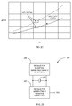
- FIG. 1A illustrates a block/schematic diagram of a conventional apparatus 100 for generating an oscillating signal.
- the conventional apparatus 100 typically comprises a negative resistance circuit 102 and a resonator coupled in a feedback configuration with the negative resistance circuit.
- the resonator in this example, includes a Xtal 104 and a pair of variable capacitors C P , typically referred to in the relevant art as Pierce capacitors.
- the variable capacitors C P serve to provide external tuning of the frequency of the oscillating signal generated by the apparatus 100 .
- FIG. 1B illustrates a graph of an impedance versus frequency of the resonator of the conventional apparatus 100 . If, for example, the Pierce capacitors C P of the conventional oscillator 100 are removed, the frequency of the oscillating signal is dictated substantially by the Xtal 104 . In such a case, the frequency of the oscillating signal falls substantially on the parallel resonance of the Xtal 104 , as indicated in the graph. At the parallel resonance, the power drawn by the negative resistance circuit 102 is substantially minimized because the impedance of the resonator is substantially maximized.
- the parallel resonance for the Xtal does not significantly change from lot-to-lot. If the tolerance of the parallel resonance is within the frequency deviation specification of the oscillator 100 , then the Pierce capacitors C P need not be required, and the oscillator may be operated in a power efficient manner. However, such a precise Xtal 104 is typically very expensive. Thus, in order to reduce cost of the oscillator 100 , a less precise and cheaper Xtal 104 may be employed. This may have the adverse consequence of the parallel resonance of the Xtal 104 from lot-to-lot varying more than the frequency deviation specification of the oscillator 100 . In such a case, frequency tuning may be required, thereby, mandating the use of one or more variable capacitors C P .
- the effects of adding capacitance C P to the resonator of the oscillator 100 is to decrease the frequency of the oscillating signal. This has the consequence of lowering the impedance of the resonator from the impedance associated with the parallel resonance of the Xtal 104 towards the impedance associated with the series resonance of the Xtal, as indicated by the oscillator tunable range in the graph. As the impedance of the resonator moves closer to the series resonance of the Xtal 104 , the negative resistance circuit 102 consumes more power.
- the power consumption is related to the pullability or frequency difference between the parallel resonance and the series resonance of the Xtal 104 .
- the power consumption of the oscillator 100 is less if the pullability is larger.
- the power consumption of the oscillator 100 is more if the pullability is smaller.
- An aspect of the disclosure relates to an apparatus for generating an oscillating signal comprising a negative-resistance circuit, a crystal, and a component adapted to modify a series resonance of the crystal to decrease power consumption of the negative-resistance circuit in generating the oscillating signal.
- the component comprises a positive-reactance circuit.
- the component comprises one or more inductive elements.
- the component comprises a pair of inductive elements coupled respectively to both sides of the crystal.
- the apparatus for generating an oscillating signal further comprises a frequency-tuning component for adjusting the frequency of the oscillating signal.
- the frequency-tuning component is adapted to adjust the frequency of the oscillating signal to be within ⁇ 10 parts-per-million (ppm) of a defined frequency.
- the frequency-tuning component comprises one or more variable capacitive elements coupled to the crystal.
- the negative-resistance circuit is configured to consume less current for a given capacitance of the one or more variable capacitive elements. In yet another aspect, the negative-resistance circuit is configured to consume less power for a given capacitance of the one or more variable capacitive elements. In still another aspect, the negative-resistance circuit comprises a digital inverter circuit, an inverting analog amplifier, or a self-regulating circuit.
- the apparatus for generating an oscillating signal comprises a quiescent current source adapted to supply a substantially steady-state current to a negative-resistance circuit, and a start up current source adapted to supply a boost current to the negative-resistance circuit only during an initiation of the oscillating signal to expedite the oscillating signal in reaching a predefined steady-state condition from a cold start.
- FIG. 1A illustrates a block/schematic diagram of a conventional apparatus for generating an oscillating signal.
- FIG. 1B illustrates a graph of an impedance versus frequency of a resonator of the conventional apparatus for generating an oscillating signal.
- FIG. 2A illustrates a block/schematic diagram of an exemplary apparatus for generating an oscillating signal in accordance with an aspect of the disclosure.
- FIG. 2B illustrates a graph of an impedance versus frequency response (solid line) of the resonator of the exemplary apparatus in accordance with another aspect of the disclosure, and the corresponding response (dashed line) of the conventional apparatus.
- FIG. 2C illustrates a graph of a critical transconductance (gmcrit) versus Pierce capacitance (C P ) response (solid line) of the resonator of the exemplary apparatus in accordance with another aspect of the disclosure, and the corresponding response (dashed line) of the resonator of the conventional apparatus.
- gmcrit critical transconductance
- C P Pierce capacitance
- FIG. 2D illustrates a block/schematic diagram of an exemplary apparatus for generating an oscillating signal in accordance with an aspect of the disclosure.
- FIG. 3A illustrates a block/schematic diagram of another exemplary apparatus for generating an oscillating signal in accordance with another aspect of the disclosure.
- FIG. 3B illustrates a block/schematic diagram of another exemplary apparatus for generating an oscillating signal in accordance with another aspect of the disclosure.
- FIG. 4A illustrates a schematic diagram of another exemplary apparatus for generating an oscillating signal in accordance with another aspect of the disclosure.
- FIG. 4B illustrates a schematic diagram of another exemplary apparatus for generating an oscillating signal in accordance with another aspect of the disclosure.
- FIG. 4C illustrates a schematic diagram of another exemplary apparatus for generating an oscillating signal in accordance with another aspect of the disclosure.
- FIG. 4D illustrates a block/schematic diagram of another exemplary apparatus for generating an oscillating signal in accordance with another aspect of the disclosure.
- FIG. 5 illustrates a block diagram of an exemplary communication system in accordance with another aspect of the disclosure.
- FIGS. 6A-D illustrate timing diagrams of various pulse modulation techniques in accordance with another aspect of the disclosure.
- FIG. 7 illustrates a block diagram of various communications devices communicating with each other via various channels in accordance with another aspect of the disclosure.
- FIG. 2A illustrates a block/schematic diagram of another exemplary apparatus 200 for generating an oscillating signal in accordance with another aspect of the disclosure.
- the apparatus 200 includes a component for lowering the series resonance of the Xtal without significantly affecting the parallel resonance of the Xtal. This has the effect of increasing the pullability range or frequency difference between the parallel resonance and series resonance of the Xtal. And, this has the ultimate effect of reducing the power consumption of the apparatus 200 for a given frequency or frequency range of the oscillating signal.
- the apparatus 200 comprises a negative-resistance circuit 202 , a Xtal 204 , and a component 206 adapted to modify a series resonance of the Xtal 204 to decrease the power consumption of the negative-resistance circuit in generating the oscillating signal.
- the Xtal 204 and the component 206 are electrically coupled to each other to form a resonator.
- the resonator is electrically coupled to the negative-resistance circuit 202 in a feedback manner in order to initiate and generate the oscillating signal.
- the component 206 modifies the series resonance of the Xtal 204 in order to increase the pullability of the resonator, and thus, decrease the power consumption of the apparatus 200 for a given frequency or frequency range of the oscillating signal, as further explained below.
- FIG. 2B illustrates a graph of an impedance versus frequency response (solid line) of the resonator of the exemplary apparatus 200 , and the corresponding response (dashed line) of the conventional apparatus 100 .
- the addition of the component 206 has the effect of lowering the series resonance of the Xtal 204 , but does not significantly affect the parallel resonance of the Xtal.
- the “new series resonance” of the Xtal 204 of the apparatus 200 is substantially less than the “old series resonance” of the Xtal 104 of the conventional apparatus 100 .
- the “new parallel resonance” of the Xtal 204 of the apparatus 200 is substantially the same as the “old parallel resonance” of the Xtal 104 of the conventional apparatus 100 , as noted in the graph.
- the “new pullability” associated with the apparatus 200 is substantially greater than the “old pullability” associated with the conventional apparatus 100 .
- the net impedance of the resonator of apparatus 200 is greater than the net impedance of the resonator of the apparatus 100 , over the oscillator tunable range as indicated in the graph. Since power consumption is inversely related to the impedance of the resonator, the apparatus 200 consumes less power than the conventional apparatus 100 for a given frequency or frequency range of the oscillating signal. As the graph illustrates, the power consumption saving improves as the frequency of the oscillating signal is tuned closer to the series resonance.
- FIG. 2C illustrates a graph of a critical transconductance (gmcrit) versus Pierce capacitance (C P ) response (solid line) of the resonator of the exemplary apparatus 200 , and the corresponding response (dashed line) of the resonator of the conventional apparatus 100 .
- the critical transconductance gmcrit is substantially the minimum transconductance of the negative-resistance circuit required for the apparatus to generate the oscillating signal.
- the critical transconductance gmcrit is directly (non-inversely) related to the power consumption of the apparatus.
- the gmcrit v. C P response for the apparatus 200 is substantially lower than the corresponding response for the conventional apparatus 100 .
- the apparatus 200 consumes substantially less power than the conventional apparatus 100 .
- the slope of the gmcrit v. C P response for the apparatus 200 is substantially lower than the slope of the corresponding response for the conventional apparatus 100 .
- a lower range of Pierce capacitance C P variation is achieved with the apparatus 200 as compared to that of the conventional apparatus 100 .
- FIG. 2D illustrates a block/schematic diagram of an exemplary apparatus 250 for generating an oscillating signal in accordance with an aspect of the disclosure.
- the apparatus 250 comprises a module 252 for generating a negative resistance, a Xtal 254 , and a module 256 for modifying the series resonance of the Xtal 254 . More specifically, the module 256 lowers the series resonance of the Xtal, without significantly affecting the parallel resonance of the Xtal. This has the effect of increasing the pullability range or frequency difference between the parallel resonance and series resonance of the Xtal. And, this has the ultimate effect of reducing the power consumption of the apparatus 250 for a given frequency or frequency range of the oscillating signal.
- FIG. 3A illustrates a block/schematic diagram of another exemplary apparatus 300 for generating an oscillating signal in accordance with another aspect of the disclosure.
- the apparatus 300 employs an inductive element as the component adapted to modify a series resonance of a Xtal for the purpose of decreasing the power consumption of the negative-resistance circuit in generating the oscillating signal.
- the apparatus 300 comprises a negative-resistance circuit 302 , a Xtal 304 , a variable capacitor C P , and an inductive element L (e.g., an inductor).
- the Xtal 304 is electrically coupled in series with the inductive element L
- the variable capacitor C P is electrically coupled between the inductive element L and ground. All of these elements (Xtal, L, and C P ) collectively form a resonator.
- the resonator is electrically coupled to the negative-resistance circuit 302 in a feedback manner in order to initiate and generate the oscillating signal.
- the inductive element L modifies the series resonance of the Xtal 304 in order to increase the pullability of the resonator, and thus, decrease the power consumption of the apparatus 300 for a given frequency or frequency range of the oscillating signal, as previously discussed.
- FIG. 3B illustrates a block/schematic diagram of another exemplary apparatus 350 for generating an oscillating signal in accordance with another aspect of the disclosure.
- the apparatus 350 employs a pair of inductive elements for modifying a series resonance of a Xtal for the purpose of decreasing the power consumption of the negative-resistance circuit in generating the oscillating signal.
- the apparatus 300 comprises a negative-resistance circuit 352 , a Xtal 354 , a pair of variable capacitors C P , and a pair of inductive elements L/2 (e.g., one or more inductors).
- the inductive elements L/2 are coupled respectively to both sides of the Xtal 354
- the variable capacitors C P are electrically coupled respectively between the inductive elements L/2 and ground. All of these elements (Xtal, L/2, and C P ) collectively form a resonator.
- the resonator is electrically coupled to the negative-resistance circuit 352 in a feedback manner in order to initiate and generate the oscillating signal.
- the pair of inductive elements L/2 modify the series resonance of the Xtal 354 in order to increase the pullability of the resonator, and thus, decrease the power consumption of the apparatus 350 for a given frequency or frequency range of the oscillating signal, as previously discussed.
- FIG. 4A illustrates a schematic diagram of another exemplary apparatus 400 for generating an oscillating signal in accordance with another aspect of the disclosure.
- the apparatus 400 includes a negative-resistance circuit in the form of a digital inverter circuit and further employs a pair of inductive elements for modifying a series resonance of a Xtal for the purpose of decreasing the power consumption of the digital inverter circuit in generating the oscillating signal.
- the apparatus 400 comprises a digital inverter circuit 402 , a Xtal 404 , a pair of variable capacitors C P , and a pair of inductive elements L/2 (e.g., one or more inductors).
- the inductive elements L/2 are coupled respectively to both sides of the Xtal 404
- the variable capacitors C P are electrically coupled respectively between the inductive elements L/2 and ground. All of these elements (Xtal, L/2, C P ) collectively form a resonator.
- the resonator is electrically coupled to the digital inverter circuit 402 in a feedback manner in order to initiate and generate the oscillating signal.
- the pair of inductive elements L/2 modify the series resonance of the Xtal 404 in order to increase the pullability of the resonator, and thus, decrease the power consumption of the apparatus 400 for a given frequency or frequency range of the oscillating signal, as previously discussed.
- FIG. 4B illustrates a schematic diagram of another exemplary apparatus 420 for generating an oscillating signal in accordance with another aspect of the disclosure.
- the apparatus 420 includes a negative-resistance circuit in the form of an inverting analog amplifier and further employs a pair of inductive elements for modifying a series resonance of a Xtal for the purpose of decreasing the power consumption of the inverting analog amplifier in generating the oscillating signal.
- the apparatus 420 comprises an inverting analog amplifier 422 , a Xtal 404 , a pair of variable capacitors C P , and a pair of inductive elements L/2 (e.g., one or more inductors).
- the inductive elements L/2 are coupled respectively to both sides of the Xtal 404
- the variable capacitors C P are electrically coupled respectively between the inductive elements L/2 and ground. All of these elements (Xtal, L/2, C P ) collectively form a resonator.
- the resonator is electrically coupled to the output and inverting input of the inverting analog amplifier 422 in order to initiate and generate the oscillating signal.
- the non-inverting input of the amplifier 422 may be connected to ground.
- the amplifier 422 may receive power from a positive (+V) and negative ( ⁇ V) power supply voltage.
- the pair of inductive elements L/2 modify the series resonance of the Xtal 404 in order to increase the pullability of the resonator, and thus, decrease the power consumption of the apparatus 420 for a given frequency or frequency range of the oscillating signal, as previously discussed.
- FIG. 4C illustrates a schematic diagram of another exemplary apparatus 440 for generating an oscillating signal in accordance with another aspect of the disclosure.
- the apparatus 440 includes a negative-resistance circuit in the form of a self-regulating circuit and further employs a pair of inductive elements for modifying a series resonance of a Xtal for the purpose of decreasing the power consumption of the self-regulating circuit in generating the oscillating signal.
- the apparatus 440 comprises a resonator including a Xtal 404 , a pair of variable capacitors C P , and a pair of inductive elements L/2 (e.g., one or more inductors).
- the inductive elements L/2 are coupled respectively to both sides of the Xtal 404
- the variable capacitors C P are electrically coupled respectively between the inductive elements L/2 and ground.
- the resonator is electrically coupled to the self-regulating circuit in a feedback configuration in order to initiate and generate the oscillating signal.
- the self-regulating circuit comprises an active device M (e.g., a metal oxide semiconductor field effect transistor (MOSFET)), a resistor R, a current mirror 442 , and a low pass filter (LPF) 446 .
- the current mirror 442 is electrically coupled between a power supply rail Vdd and the drain of the active device M.
- the resistor R is electrically coupled between the drain and gate of the active device M, which has a source connected to a negative power supply rail Vss.
- the LPF 446 is electrically coupled between the gate of the active device M and the current mirror M.
- the self-regulation circuit regulates the current supplied to the active device M in response to the amplitude of the oscillating signal at the gate of the active device M.
- the resonator is coupled between the drain and gate of the active device M.
- the pair of inductive elements L/2 modify the series resonance of the Xtal 404 in order to increase the pullability of the resonator, and thus, decrease the power consumption of the apparatus 440 for a given frequency or frequency range of the oscillating signal, as previously discussed.
- the apparatus 440 further includes an oscillation detector 448 adapted to generate a signal indicative of whether the oscillating signal is being generated. Additionally, the apparatus 440 includes an amplifier 450 adapted to amplify the oscillating signal.
- FIG. 4D illustrates a block/schematic diagram of another exemplary apparatus 460 for generating an oscillating signal in accordance with another aspect of the disclosure.
- the apparatus 460 includes a quiescent power source adapted to supply a substantially steady-state current to a negative-resistance circuit for continued generation of the oscillating signal, and a start-up boost power source for supplying a boost current only during start up in order to expedite the oscillating signal reaching a defined steady-state condition.
- the apparatus 460 includes a pair of inductive elements for modifying a series resonance of a Xtal for the purpose of decreasing the power consumption of the negative-resistance circuit in generating the oscillating signal.
- the apparatus 460 comprises a quiescent power source 466 , a start-up boost power source 468 , a negative-resistance circuit 464 , a Xtal 404 , a pair of variable capacitors C P , and a pair of inductive elements L/2 (e.g., one or more inductors).
- the inductive elements L/2 are coupled respectively to both sides of the Xtal 404
- the variable capacitors C P are electrically coupled respectively between the inductive elements L/2 and ground. All of these elements (Xtal, L/2, and C P ) collectively form a resonator.
- the resonator in turn, is electrically coupled to the negative-resistance circuit 464 in a feedback configuration in order to initiate and generate the oscillating signal.
- the pair of inductive elements L/2 modify the series resonance of the Xtal 404 in order to increase the pullability of the resonator, and thus, decrease the power consumption of the apparatus 460 for a given frequency or frequency range of the oscillating signal, as previously discussed.
- the quiescent power source 466 is adapted to supply a substantially steady-state current I 1 to the negative-resistance circuit 464 in order for the latter to continuously generate the oscillating signal.
- the start-up boost power source 468 is adapted to supply a boost current I 2 only during start up in order to expedite the oscillating signal in reaching a defined steady-state condition from a cold start.
- the steady-state condition may be a defined amplitude stability and/or a defined frequency stability.
- FIG. 5 illustrates a block diagram of an exemplary communication device 500 in accordance with another aspect of the disclosure.
- the communication device 500 may be one exemplary implementation of a communication device that uses any of the apparatuses previously discussed as a reference oscillator.
- the communications device 500 comprises an antenna 502 , a Tx/Rx isolation device 504 , a low noise amplifier (LNA) 506 , a downconverter and/or demodulator 508 , a receiver baseband processing module 510 , a phase locked loop (PLL) and/or voltage controlled oscillator (VCO) 512 , a reference oscillator 514 , a transmitter baseband processing module 516 , an upconverter and/or modulator 518 , and a power amplifier (PA) 520 .
- LNA low noise amplifier
- VCO voltage controlled oscillator
- data to be transmitted to a destination communication device is sent to the transmitter baseband processing module 516 .
- the transmitter baseband processing module 516 processes the transmit data to generate an outgoing baseband signal.
- the upconverter and/or modulator 518 uses a local oscillator or signal generated by the PLL and/or VCO 512 with the use of the reference oscillator 514 , processes the outgoing baseband signal to generate an RF signal.
- the PA 520 amplifies the RF signal and provides it to the antenna 502 via the Tx/Rx isolation device 504 for transmission into a wireless medium.
- the transmit data may be generated by a sensor, a microprocessor, a microcontroller, a RISC processor, a keyboard, a pointing device such as a mouse or a track ball, an audio device, such as a headset, including a transducer such as a microphone, a medical device, a shoe, a robotic or mechanical device that generates data, a user interface, such as a touch-sensitive display, etc.
- a sensor a microprocessor, a microcontroller, a RISC processor, a keyboard, a pointing device such as a mouse or a track ball, an audio device, such as a headset, including a transducer such as a microphone, a medical device, a shoe, a robotic or mechanical device that generates data, a user interface, such as a touch-sensitive display, etc.
- the reference oscillator 514 may be used in other types of application, such as a clock source to drive digital and/or analog circuitry.
- an RF signal carrying data is picked up by the antenna 502 and applied to the LNA 506 via the Tx/Rx isolation device 504 .
- the LNA 506 amplifies the received RF signal.
- the downconverter and/or demodulator 508 using a local oscillator or signal generated by the PLL and/or VCO 512 with the use of the reference oscillator 514 , processes the received RF signal to generate incoming baseband signal.
- the receiver baseband processing 510 processes the incoming baseband signal to generate the received data.
- a data processor (not shown) may then perform one or more defined operations based on the received data.
- the data processor may include a microprocessor, a microcontroller, a reduced instruction set computer (RISC) processor, a display, an audio device, such as a headset, including a transducer such as speakers, a medical device, a shoe, a watch, a robotic or mechanical device responsive to the data, a user interface, such as a display, one or more light emitting diodes (LED), etc.
- RISC reduced instruction set computer
- FIG. 6A illustrates different channels (channels 1 and 2 ) defined with different pulse repetition frequencies (PRF) as an example of a pulse modulation that may be employed in any of the communications systems, devices, and apparatuses described herein.
- pulses for channel 1 have a pulse repetition frequency (PRF) corresponding to a pulse-to-pulse delay period 602 .
- pulses for channel 2 have a pulse repetition frequency (PRF) corresponding to a pulse-to-pulse delay period 604 .
- PRF pulse repetition frequency
- PRF pulse repetition frequency
- This technique may thus be used to define pseudo-orthogonal channels with a relatively low likelihood of pulse collisions between the two channels.
- a low likelihood of pulse collisions may be achieved through the use of a low duty cycle for the pulses.
- substantially all pulses for a given channel may be transmitted at different times than pulses for any other channel.
- FIG. 6B illustrates different channels (channels 1 and 2 ) defined with different pulse positions or offsets as an example of a modulation that may be employed in any of the communications systems described herein.
- Pulses for channel 1 are generated at a point in time as represented by line 606 in accordance with a first pulse offset (e.g., with respect to a given point in time, not shown).
- pulses for channel 2 are generated at a point in time as represented by line 608 in accordance with a second pulse offset. Given the pulse offset difference between the pulses (as represented by the arrows 610 ), this technique may be used to reduce the likelihood of pulse collisions between the two channels.
- the use of different pulse offsets may be used to provide orthogonal or pseudo-orthogonal channels.
- FIG. 6C illustrates different channels (channels 1 and 2 ) defined with different timing hopping sequences modulation that may be employed in any of the communications systems described herein.
- pulses 612 for channel 1 may be generated at times in accordance with one time hopping sequence while pulses 614 for channel 2 may be generated at times in accordance with another time hopping sequence.
- this technique may be used to provide orthogonal or pseudo-orthogonal channels.
- the time hopped pulse positions may not be periodic to reduce the possibility of repeat pulse collisions from neighboring channels.
- FIG. 6D illustrates different channels defined with different time slots as an example of a pulse modulation that may be employed in any of the communications systems described herein.
- Pulses for channel L 1 are generated at particular time instances.
- pulses for channel L 2 are generated at other time instances.
- pulse for channel L 3 are generated at still other time instances.
- the time instances pertaining to the different channels do not coincide or may be orthogonal to reduce or eliminate interference between the various channels.
- a channel may be defined based on different spreading pseudo-random number sequences, or some other suitable parameter or parameters.
- a channel may be defined based on a combination of two or more parameters.
- FIG. 7 illustrates a block diagram of various ultra-wide band (UWB) communications devices communicating with each other via various channels in accordance with another aspect of the disclosure.
- UWB device 1 702 is communicating with UWB device 2 704 via two concurrent UWB channels 1 and 2 .
- UWB device 702 is communicating with UWB device 3 706 via a single channel 3 .
- UWB device 3 706 is, in turn, communicating with UWB device 4 708 via a single channel 4 .
- the communications devices may be used for many different applications, and may be implemented, for example, in a headset, microphone, biometric sensor, heart rate monitor, pedometer, EKG device, watch, shoe, remote control, switch, tire pressure monitor, or other communications devices.
- a medical device may include smart band-aid, sensors, vital sign monitors, and others.
- the communications devices described herein may be used in any type of sensing application, such as for sensing automotive, athletic, and physiological (medical) responses.
- any of the above aspects of the disclosure may be implemented in many different devices.
- the aspects of the disclosure may be applied to health and fitness applications.
- the aspects of the disclosure may be implemented in shoes for different types of applications. There are other multitude of applications that may incorporate any aspect of the disclosure as described herein.
- concurrent channels may be established based on pulse repetition frequencies.
- concurrent channels may be established based on pulse position or offsets.
- concurrent channels may be established based on time hopping sequences.
- concurrent channels may be established based on pulse repetition frequencies, pulse positions or offsets, and time hopping sequences.
- the various illustrative logical blocks, modules, and circuits described in connection with the aspects disclosed herein may be implemented within or performed by an integrated circuit (“IC”), an access terminal, or an access point.
- the IC may comprise a general purpose processor, a digital signal processor (DSP), an application specific integrated circuit (ASIC), a field programmable gate array (FPGA) or other programmable logic device, discrete gate or transistor logic, discrete hardware components, electrical components, optical components, mechanical components, or any combination thereof designed to perform the functions described herein, and may execute codes or instructions that reside within the IC, outside of the IC, or both.
- a general purpose processor may be a microprocessor, but in the alternative, the processor may be any conventional processor, controller, microcontroller, or state machine.
- a processor may also be implemented as a combination of computing devices, e.g., a combination of a DSP and a microprocessor, a plurality of microprocessors, one or more microprocessors in conjunction with a DSP core, or any other such configuration.
- a software module e.g., including executable instructions and related data
- other data may reside in a data memory such as RAM memory, flash memory, ROM memory, EPROM memory, EEPROM memory, registers, a hard disk, a removable disk, a CD-ROM, or any other form of computer-readable storage medium known in the art.
- a sample storage medium may be coupled to a machine such as, for example, a computer/processor (which may be referred to herein, for convenience, as a “processor”) such the processor can read information (e.g., code) from and write information to the storage medium.
- a sample storage medium may be integral to the processor.
- the processor and the storage medium may reside in an ASIC.
- the ASIC may reside in user equipment.
- the processor and the storage medium may reside as discrete components in user equipment.
- any suitable computer-program product may comprise a computer-readable medium comprising codes relating to one or more of the aspects of the disclosure.
- a computer program product may comprise packaging materials.
Landscapes
- Oscillators With Electromechanical Resonators (AREA)
Priority Applications (8)
| Application Number | Priority Date | Filing Date | Title |
|---|---|---|---|
| US12/467,894 US8072278B2 (en) | 2009-05-18 | 2009-05-18 | System and method for reducing power consumption of an oscillator |
| EP10717990.5A EP2433357B1 (en) | 2009-05-18 | 2010-05-05 | System and method for reducing power consumption of an oscillator |
| PCT/US2010/033681 WO2010135084A2 (en) | 2009-05-18 | 2010-05-05 | System and method for reducing power consumption of an oscillator |
| CN201080022034.0A CN102428642B (zh) | 2009-05-18 | 2010-05-05 | 用于减少振荡器的功率消耗的系统和方法 |
| JP2012511877A JP2012527826A (ja) | 2009-05-18 | 2010-05-05 | 発振器の電力消費を低減させるためのシステムおよび方法 |
| KR1020117030407A KR101392955B1 (ko) | 2009-05-18 | 2010-05-05 | 발진 신호를 생성하기 위한 장치, 방법 및 컴퓨터-판독가능 매체, 그리고 이를 이용한 디바이스들 |
| TW099114988A TW201130221A (en) | 2009-05-18 | 2010-05-11 | System and method for reducing power consumption of an oscillator |
| JP2013229851A JP5996510B2 (ja) | 2009-05-18 | 2013-11-05 | 発振器の電力消費を低減させるためのシステムおよび方法 |
Applications Claiming Priority (1)
| Application Number | Priority Date | Filing Date | Title |
|---|---|---|---|
| US12/467,894 US8072278B2 (en) | 2009-05-18 | 2009-05-18 | System and method for reducing power consumption of an oscillator |
Publications (2)
| Publication Number | Publication Date |
|---|---|
| US20100289587A1 US20100289587A1 (en) | 2010-11-18 |
| US8072278B2 true US8072278B2 (en) | 2011-12-06 |
Family
ID=42262677
Family Applications (1)
| Application Number | Title | Priority Date | Filing Date |
|---|---|---|---|
| US12/467,894 Active 2029-10-05 US8072278B2 (en) | 2009-05-18 | 2009-05-18 | System and method for reducing power consumption of an oscillator |
Country Status (7)
| Country | Link |
|---|---|
| US (1) | US8072278B2 (cg-RX-API-DMAC7.html) |
| EP (1) | EP2433357B1 (cg-RX-API-DMAC7.html) |
| JP (2) | JP2012527826A (cg-RX-API-DMAC7.html) |
| KR (1) | KR101392955B1 (cg-RX-API-DMAC7.html) |
| CN (1) | CN102428642B (cg-RX-API-DMAC7.html) |
| TW (1) | TW201130221A (cg-RX-API-DMAC7.html) |
| WO (1) | WO2010135084A2 (cg-RX-API-DMAC7.html) |
Families Citing this family (2)
| Publication number | Priority date | Publication date | Assignee | Title |
|---|---|---|---|---|
| KR101415319B1 (ko) * | 2012-08-21 | 2014-07-08 | 한국과학기술원 | 무선 송신기 및 무선 송신기를 포함하는 통신 장치 |
| JP2014096631A (ja) * | 2012-11-07 | 2014-05-22 | Nippon Dempa Kogyo Co Ltd | 自励発振回路 |
Citations (12)
| Publication number | Priority date | Publication date | Assignee | Title |
|---|---|---|---|---|
| DE1591524A1 (de) | 1966-08-09 | 1970-01-29 | Sits Soc It Telecom Siemens | Schaltungsanordnung zum Erzeugen einer frequenzmodulierten Schwingung |
| JPS5467471A (en) | 1977-11-09 | 1979-05-30 | Seiko Instr & Electronics Ltd | Electronic watch with receiver |
| US4346537A (en) | 1978-11-30 | 1982-08-31 | Tdk Electronics Co., Ltd. | Capacitor trimming system in a quartz-crystal oscillator |
| US4956618A (en) * | 1989-04-07 | 1990-09-11 | Vlsi Technology, Inc. | Start-up circuit for low power MOS crystal oscillator |
| JPH11308050A (ja) | 1998-04-20 | 1999-11-05 | Toyo Commun Equip Co Ltd | 電圧制御圧電発振器 |
| US20020125963A1 (en) * | 2001-03-08 | 2002-09-12 | Ash Darrell Lee | Low phase noise, wide tune range saw oscillators and methods of operating the same |
| US20040233000A1 (en) | 2003-05-22 | 2004-11-25 | Intel Corporation | Oscillator system with switched-capacitor network and method for generating a precision time reference |
| US20050059375A1 (en) | 2003-07-24 | 2005-03-17 | Kabushiki Kaisha Toshiba | Voltage controlled oscillator, frequency synthesizer and communication apparatus |
| US20070021087A1 (en) | 2005-07-21 | 2007-01-25 | Microsoft Corporation | Dynamic bias for receiver controlled by radio link quality |
| GB2430752A (en) | 2005-09-30 | 2007-04-04 | Avago Technologies General Ip | Sensing system with output frequency dependent on sensor capacitance |
| US20080100392A1 (en) | 2004-03-22 | 2008-05-01 | Mobius Microsystems, Inc. | Low-Latency Start-Up for a Monolithic Clock Generator and Timing/Frequency Reference |
| US20090080568A1 (en) | 2007-09-21 | 2009-03-26 | Qualcomm Incorporated | Signal generator with adjustable phase |
Family Cites Families (16)
| Publication number | Priority date | Publication date | Assignee | Title |
|---|---|---|---|---|
| JPS4979658A (cg-RX-API-DMAC7.html) * | 1972-12-07 | 1974-08-01 | ||
| JPS5810903A (ja) * | 1981-07-11 | 1983-01-21 | Tdk Corp | 圧電振動子の駆動回路 |
| JPS59196610A (ja) * | 1983-04-21 | 1984-11-08 | Matsushita Electric Ind Co Ltd | 弾性表面波発振器 |
| JPH01290303A (ja) * | 1988-05-18 | 1989-11-22 | Fujitsu Ltd | オーバートーン水晶発振回路 |
| JPH04132721U (ja) * | 1991-05-31 | 1992-12-09 | キンセキ株式会社 | 圧電発振回路 |
| JPH0568110U (ja) * | 1992-02-17 | 1993-09-10 | 横河電機株式会社 | 周波数可変発振回路 |
| JPH0654308U (ja) * | 1992-12-25 | 1994-07-22 | 日本ビクター株式会社 | 周波数変調回路 |
| JPH07154143A (ja) * | 1993-11-26 | 1995-06-16 | Nec Corp | 発振回路 |
| JPH1075119A (ja) * | 1996-08-29 | 1998-03-17 | Mitsumi Electric Co Ltd | 発振器 |
| JP2001016039A (ja) * | 1999-06-30 | 2001-01-19 | Kinseki Ltd | 可変周波数発振回路 |
| JP2005159386A (ja) * | 2003-11-07 | 2005-06-16 | Nippon Dempa Kogyo Co Ltd | オーバトーン用の水晶発振器 |
| JP2006197143A (ja) * | 2005-01-12 | 2006-07-27 | Nippon Dempa Kogyo Co Ltd | 電圧制御水晶発振器 |
| JP4494387B2 (ja) * | 2006-10-30 | 2010-06-30 | 日本電波工業株式会社 | 水晶発振器 |
| JP2008177981A (ja) * | 2007-01-22 | 2008-07-31 | Nippon Dempa Kogyo Co Ltd | 発振器 |
| US7592878B2 (en) * | 2007-04-05 | 2009-09-22 | Qualcomm Incorporated | Method and apparatus for generating oscillating signals |
| JP5023282B2 (ja) * | 2007-04-10 | 2012-09-12 | 英彰 高島 | 圧電発振器 |
-
2009
- 2009-05-18 US US12/467,894 patent/US8072278B2/en active Active
-
2010
- 2010-05-05 WO PCT/US2010/033681 patent/WO2010135084A2/en not_active Ceased
- 2010-05-05 JP JP2012511877A patent/JP2012527826A/ja not_active Withdrawn
- 2010-05-05 EP EP10717990.5A patent/EP2433357B1/en not_active Not-in-force
- 2010-05-05 CN CN201080022034.0A patent/CN102428642B/zh not_active Expired - Fee Related
- 2010-05-05 KR KR1020117030407A patent/KR101392955B1/ko active Active
- 2010-05-11 TW TW099114988A patent/TW201130221A/zh unknown
-
2013
- 2013-11-05 JP JP2013229851A patent/JP5996510B2/ja active Active
Patent Citations (12)
| Publication number | Priority date | Publication date | Assignee | Title |
|---|---|---|---|---|
| DE1591524A1 (de) | 1966-08-09 | 1970-01-29 | Sits Soc It Telecom Siemens | Schaltungsanordnung zum Erzeugen einer frequenzmodulierten Schwingung |
| JPS5467471A (en) | 1977-11-09 | 1979-05-30 | Seiko Instr & Electronics Ltd | Electronic watch with receiver |
| US4346537A (en) | 1978-11-30 | 1982-08-31 | Tdk Electronics Co., Ltd. | Capacitor trimming system in a quartz-crystal oscillator |
| US4956618A (en) * | 1989-04-07 | 1990-09-11 | Vlsi Technology, Inc. | Start-up circuit for low power MOS crystal oscillator |
| JPH11308050A (ja) | 1998-04-20 | 1999-11-05 | Toyo Commun Equip Co Ltd | 電圧制御圧電発振器 |
| US20020125963A1 (en) * | 2001-03-08 | 2002-09-12 | Ash Darrell Lee | Low phase noise, wide tune range saw oscillators and methods of operating the same |
| US20040233000A1 (en) | 2003-05-22 | 2004-11-25 | Intel Corporation | Oscillator system with switched-capacitor network and method for generating a precision time reference |
| US20050059375A1 (en) | 2003-07-24 | 2005-03-17 | Kabushiki Kaisha Toshiba | Voltage controlled oscillator, frequency synthesizer and communication apparatus |
| US20080100392A1 (en) | 2004-03-22 | 2008-05-01 | Mobius Microsystems, Inc. | Low-Latency Start-Up for a Monolithic Clock Generator and Timing/Frequency Reference |
| US20070021087A1 (en) | 2005-07-21 | 2007-01-25 | Microsoft Corporation | Dynamic bias for receiver controlled by radio link quality |
| GB2430752A (en) | 2005-09-30 | 2007-04-04 | Avago Technologies General Ip | Sensing system with output frequency dependent on sensor capacitance |
| US20090080568A1 (en) | 2007-09-21 | 2009-03-26 | Qualcomm Incorporated | Signal generator with adjustable phase |
Non-Patent Citations (3)
| Title |
|---|
| International Search Report and Written Opinion-PCT/US2010/033681, International Search Authority-European Patent Office-Jan. 21, 2011. |
| Partial International Search Report-PCT/US2010/033681, International Searching Authority, European Patent Office, Aug. 10, 2010. |
| Trimming the Crystal Frequency in: Robert Matthys: "Crystal Oscillator Circuits", 1992, Krieger Publishing Company, Malabar, Florida, XP002614715, ISBN: 0-89464-552-8 pp. 101-102. |
Also Published As
| Publication number | Publication date |
|---|---|
| JP2012527826A (ja) | 2012-11-08 |
| KR20120024801A (ko) | 2012-03-14 |
| US20100289587A1 (en) | 2010-11-18 |
| JP5996510B2 (ja) | 2016-09-21 |
| WO2010135084A2 (en) | 2010-11-25 |
| CN102428642A (zh) | 2012-04-25 |
| TW201130221A (en) | 2011-09-01 |
| WO2010135084A3 (en) | 2011-03-17 |
| CN102428642B (zh) | 2015-09-30 |
| KR101392955B1 (ko) | 2014-05-09 |
| JP2014064295A (ja) | 2014-04-10 |
| EP2433357A2 (en) | 2012-03-28 |
| EP2433357B1 (en) | 2015-09-30 |
Similar Documents
| Publication | Publication Date | Title |
|---|---|---|
| US8188802B2 (en) | System and method for efficiently generating an oscillating signal | |
| KR101157317B1 (ko) | 발진기 및 발진 개시 방법 | |
| US8319562B2 (en) | System and method for amplifying a signal using multiple amplification stages sharing a common bias current | |
| US10312860B2 (en) | Reducing duration of start-up period for a crystal oscillator circuit | |
| KR101343026B1 (ko) | 펄스 생성기를 전력 캘리브레이팅하기 위한 시스템 및 방법 | |
| US9515606B2 (en) | Oscillator and radio communication device | |
| EP2391036B1 (en) | Spectrum spreaders including tunable filters and related devices and methods | |
| CN103199859A (zh) | 时钟产生器及移动设备 | |
| US8072278B2 (en) | System and method for reducing power consumption of an oscillator | |
| US8811919B2 (en) | System and method for generating a defined pulse | |
| US20090215391A1 (en) | Apparatus and method for compensating inductance in inductive coupling communications |
Legal Events
| Date | Code | Title | Description |
|---|---|---|---|
| AS | Assignment |
Owner name: QUALCOMM INCORPORATED, CALIFORNIA Free format text: ASSIGNMENT OF ASSIGNORS INTEREST;ASSIGNORS:GARCIA, JORGE A.;MOYER, TODD;REEL/FRAME:022698/0987 Effective date: 20090518 |
|
| STCF | Information on status: patent grant |
Free format text: PATENTED CASE |
|
| FPAY | Fee payment |
Year of fee payment: 4 |
|
| MAFP | Maintenance fee payment |
Free format text: PAYMENT OF MAINTENANCE FEE, 8TH YEAR, LARGE ENTITY (ORIGINAL EVENT CODE: M1552); ENTITY STATUS OF PATENT OWNER: LARGE ENTITY Year of fee payment: 8 |
|
| MAFP | Maintenance fee payment |
Free format text: PAYMENT OF MAINTENANCE FEE, 12TH YEAR, LARGE ENTITY (ORIGINAL EVENT CODE: M1553); ENTITY STATUS OF PATENT OWNER: LARGE ENTITY Year of fee payment: 12 |