US8071405B2 - Group-III nitride semiconductor laser device, and method for fabricating group-III nitride semiconductor laser device - Google Patents
Group-III nitride semiconductor laser device, and method for fabricating group-III nitride semiconductor laser device Download PDFInfo
- Publication number
- US8071405B2 US8071405B2 US12/836,281 US83628110A US8071405B2 US 8071405 B2 US8071405 B2 US 8071405B2 US 83628110 A US83628110 A US 83628110A US 8071405 B2 US8071405 B2 US 8071405B2
- Authority
- US
- United States
- Prior art keywords
- iii nitride
- nitride semiconductor
- group
- axis
- laser
- Prior art date
- Legal status (The legal status is an assumption and is not a legal conclusion. Google has not performed a legal analysis and makes no representation as to the accuracy of the status listed.)
- Expired - Fee Related
Links
Images


Classifications
-
- H—ELECTRICITY
- H01—ELECTRIC ELEMENTS
- H01S—DEVICES USING THE PROCESS OF LIGHT AMPLIFICATION BY STIMULATED EMISSION OF RADIATION [LASER] TO AMPLIFY OR GENERATE LIGHT; DEVICES USING STIMULATED EMISSION OF ELECTROMAGNETIC RADIATION IN WAVE RANGES OTHER THAN OPTICAL
- H01S5/00—Semiconductor lasers
- H01S5/10—Construction or shape of the optical resonator, e.g. extended or external cavity, coupled cavities, bent-guide, varying width, thickness or composition of the active region
-
- H—ELECTRICITY
- H01—ELECTRIC ELEMENTS
- H01S—DEVICES USING THE PROCESS OF LIGHT AMPLIFICATION BY STIMULATED EMISSION OF RADIATION [LASER] TO AMPLIFY OR GENERATE LIGHT; DEVICES USING STIMULATED EMISSION OF ELECTROMAGNETIC RADIATION IN WAVE RANGES OTHER THAN OPTICAL
- H01S5/00—Semiconductor lasers
- H01S5/30—Structure or shape of the active region; Materials used for the active region
- H01S5/34—Structure or shape of the active region; Materials used for the active region comprising quantum well or superlattice structures, e.g. single quantum well [SQW] lasers, multiple quantum well [MQW] lasers or graded index separate confinement heterostructure [GRINSCH] lasers
- H01S5/343—Structure or shape of the active region; Materials used for the active region comprising quantum well or superlattice structures, e.g. single quantum well [SQW] lasers, multiple quantum well [MQW] lasers or graded index separate confinement heterostructure [GRINSCH] lasers in AIIIBV compounds, e.g. AlGaAs-laser, InP-based laser
- H01S5/34333—Structure or shape of the active region; Materials used for the active region comprising quantum well or superlattice structures, e.g. single quantum well [SQW] lasers, multiple quantum well [MQW] lasers or graded index separate confinement heterostructure [GRINSCH] lasers in AIIIBV compounds, e.g. AlGaAs-laser, InP-based laser with a well layer based on Ga(In)N or Ga(In)P, e.g. blue laser
-
- B—PERFORMING OPERATIONS; TRANSPORTING
- B82—NANOTECHNOLOGY
- B82Y—SPECIFIC USES OR APPLICATIONS OF NANOSTRUCTURES; MEASUREMENT OR ANALYSIS OF NANOSTRUCTURES; MANUFACTURE OR TREATMENT OF NANOSTRUCTURES
- B82Y20/00—Nanooptics, e.g. quantum optics or photonic crystals
-
- H—ELECTRICITY
- H01—ELECTRIC ELEMENTS
- H01S—DEVICES USING THE PROCESS OF LIGHT AMPLIFICATION BY STIMULATED EMISSION OF RADIATION [LASER] TO AMPLIFY OR GENERATE LIGHT; DEVICES USING STIMULATED EMISSION OF ELECTROMAGNETIC RADIATION IN WAVE RANGES OTHER THAN OPTICAL
- H01S5/00—Semiconductor lasers
- H01S5/02—Structural details or components not essential to laser action
- H01S5/0201—Separation of the wafer into individual elements, e.g. by dicing, cleaving, etching or directly during growth
- H01S5/0202—Cleaving
-
- H—ELECTRICITY
- H01—ELECTRIC ELEMENTS
- H01S—DEVICES USING THE PROCESS OF LIGHT AMPLIFICATION BY STIMULATED EMISSION OF RADIATION [LASER] TO AMPLIFY OR GENERATE LIGHT; DEVICES USING STIMULATED EMISSION OF ELECTROMAGNETIC RADIATION IN WAVE RANGES OTHER THAN OPTICAL
- H01S5/00—Semiconductor lasers
- H01S5/30—Structure or shape of the active region; Materials used for the active region
- H01S5/32—Structure or shape of the active region; Materials used for the active region comprising PN junctions, e.g. hetero- or double- heterostructures
- H01S5/3202—Structure or shape of the active region; Materials used for the active region comprising PN junctions, e.g. hetero- or double- heterostructures grown on specifically orientated substrates, or using orientation dependent growth
- H01S5/320275—Structure or shape of the active region; Materials used for the active region comprising PN junctions, e.g. hetero- or double- heterostructures grown on specifically orientated substrates, or using orientation dependent growth semi-polar orientation
-
- H—ELECTRICITY
- H01—ELECTRIC ELEMENTS
- H01L—SEMICONDUCTOR DEVICES NOT COVERED BY CLASS H10
- H01L21/00—Processes or apparatus adapted for the manufacture or treatment of semiconductor or solid state devices or of parts thereof
- H01L21/02—Manufacture or treatment of semiconductor devices or of parts thereof
- H01L21/02104—Forming layers
- H01L21/02365—Forming inorganic semiconducting materials on a substrate
- H01L21/02367—Substrates
- H01L21/0237—Materials
- H01L21/02387—Group 13/15 materials
- H01L21/02389—Nitrides
-
- H—ELECTRICITY
- H01—ELECTRIC ELEMENTS
- H01L—SEMICONDUCTOR DEVICES NOT COVERED BY CLASS H10
- H01L21/00—Processes or apparatus adapted for the manufacture or treatment of semiconductor or solid state devices or of parts thereof
- H01L21/02—Manufacture or treatment of semiconductor devices or of parts thereof
- H01L21/02104—Forming layers
- H01L21/02365—Forming inorganic semiconducting materials on a substrate
- H01L21/02367—Substrates
- H01L21/02433—Crystal orientation
-
- H—ELECTRICITY
- H01—ELECTRIC ELEMENTS
- H01L—SEMICONDUCTOR DEVICES NOT COVERED BY CLASS H10
- H01L21/00—Processes or apparatus adapted for the manufacture or treatment of semiconductor or solid state devices or of parts thereof
- H01L21/02—Manufacture or treatment of semiconductor devices or of parts thereof
- H01L21/02104—Forming layers
- H01L21/02365—Forming inorganic semiconducting materials on a substrate
- H01L21/02436—Intermediate layers between substrates and deposited layers
- H01L21/02439—Materials
- H01L21/02455—Group 13/15 materials
- H01L21/02458—Nitrides
-
- H—ELECTRICITY
- H01—ELECTRIC ELEMENTS
- H01L—SEMICONDUCTOR DEVICES NOT COVERED BY CLASS H10
- H01L21/00—Processes or apparatus adapted for the manufacture or treatment of semiconductor or solid state devices or of parts thereof
- H01L21/02—Manufacture or treatment of semiconductor devices or of parts thereof
- H01L21/02104—Forming layers
- H01L21/02365—Forming inorganic semiconducting materials on a substrate
- H01L21/02518—Deposited layers
- H01L21/02521—Materials
- H01L21/02538—Group 13/15 materials
- H01L21/0254—Nitrides
-
- H—ELECTRICITY
- H01—ELECTRIC ELEMENTS
- H01L—SEMICONDUCTOR DEVICES NOT COVERED BY CLASS H10
- H01L21/00—Processes or apparatus adapted for the manufacture or treatment of semiconductor or solid state devices or of parts thereof
- H01L21/02—Manufacture or treatment of semiconductor devices or of parts thereof
- H01L21/02104—Forming layers
- H01L21/02365—Forming inorganic semiconducting materials on a substrate
- H01L21/02612—Formation types
- H01L21/02617—Deposition types
- H01L21/0262—Reduction or decomposition of gaseous compounds, e.g. CVD
-
- H—ELECTRICITY
- H01—ELECTRIC ELEMENTS
- H01S—DEVICES USING THE PROCESS OF LIGHT AMPLIFICATION BY STIMULATED EMISSION OF RADIATION [LASER] TO AMPLIFY OR GENERATE LIGHT; DEVICES USING STIMULATED EMISSION OF ELECTROMAGNETIC RADIATION IN WAVE RANGES OTHER THAN OPTICAL
- H01S5/00—Semiconductor lasers
- H01S5/0014—Measuring characteristics or properties thereof
-
- H—ELECTRICITY
- H01—ELECTRIC ELEMENTS
- H01S—DEVICES USING THE PROCESS OF LIGHT AMPLIFICATION BY STIMULATED EMISSION OF RADIATION [LASER] TO AMPLIFY OR GENERATE LIGHT; DEVICES USING STIMULATED EMISSION OF ELECTROMAGNETIC RADIATION IN WAVE RANGES OTHER THAN OPTICAL
- H01S5/00—Semiconductor lasers
- H01S5/10—Construction or shape of the optical resonator, e.g. extended or external cavity, coupled cavities, bent-guide, varying width, thickness or composition of the active region
- H01S5/1082—Construction or shape of the optical resonator, e.g. extended or external cavity, coupled cavities, bent-guide, varying width, thickness or composition of the active region with a special facet structure, e.g. structured, non planar, oblique
-
- H—ELECTRICITY
- H01—ELECTRIC ELEMENTS
- H01S—DEVICES USING THE PROCESS OF LIGHT AMPLIFICATION BY STIMULATED EMISSION OF RADIATION [LASER] TO AMPLIFY OR GENERATE LIGHT; DEVICES USING STIMULATED EMISSION OF ELECTROMAGNETIC RADIATION IN WAVE RANGES OTHER THAN OPTICAL
- H01S5/00—Semiconductor lasers
- H01S5/30—Structure or shape of the active region; Materials used for the active region
- H01S5/32—Structure or shape of the active region; Materials used for the active region comprising PN junctions, e.g. hetero- or double- heterostructures
- H01S5/3211—Structure or shape of the active region; Materials used for the active region comprising PN junctions, e.g. hetero- or double- heterostructures characterised by special cladding layers, e.g. details on band-discontinuities
Definitions
- the present invention relates to a group-III nitride semiconductor laser device, and a method for fabricating the group-III nitride semiconductor laser device.
- Non-patent Document 1 Jpn. J. Appl. Phys. Vol. 35, (1996) L74-L76 describes a semiconductor laser made on a c-plane sapphire substrate.
- the mirror faces of the semiconductor laser are formed by dry etching.
- the Document 1 shows micrographs of the laser cavity mirror faces of the laser, and describes that the roughness of the end faces is about 50 nm.
- Non-patent Document 2 (Appl. Phys. Express 1 (2008) 091102) describes a semiconductor laser formed on a (11-22) plane GaN substrate. The mirror faces of the semiconductor laser are formed by dry etching.
- Non-patent Document 3 Jpn. J. Appl. Phys. Vol. 46, (2007) L789 describes a gallium nitride (GaN)-based semiconductor laser. It proposes generation of laser light polarized in an off direction of the c-axis of the substrate, in order to use m-plane cleaved facets for the laser cavity. Specifically, this Document describes increase of the well thickness on a nonpolar surface and decrease of the well thickness on a semipolar surface.
- GaN gallium nitride
- the band structure of the GaN-based semiconductor has some possible transitions capable of lasing. According to the Inventor's knowledge, it is considered that in the group-III nitride semiconductor laser device using the semipolar-plane support base the c-axis of which is inclined toward the m-axis, the threshold current can be lowered when the laser waveguide extends along a plane defined by the c-axis and the m-axis. When the laser waveguide extends in this orientation, a mode with the smallest transition energy (difference between conduction band energy and valence band energy) among the above possible transitions becomes capable of lasing; when this mode becomes capable of lasing, the threshold current can be reduced.
- this orientation of the laser waveguide does not allow use of the conventional cleaved facets such as c-planes, a-planes, or m-planes for the laser cavity mirrors.
- the laser cavity mirrors have been made heretofore by forming dry-etched facets of semiconductor layers by reactive ion etching (RIE).
- RIE reactive ion etching
- the present invention has been accomplished in view of the above-described circumstances. It is an object of the present invention to provide a group-III nitride semiconductor laser device with a laser cavity enabling a low threshold current, on the semipolar surface of a support base that tilts with respect to the c-axis toward the m-axis of a hexagonal group-III nitride. It is another object of the present invention to provide a method of fabricating the group-III nitride semiconductor laser device.
- a group-III nitride semiconductor laser device comprises: (a) a laser structure including a support base and a semiconductor region, the support base comprising a hexagonal group-III nitride semiconductor and having a semipolar principal surface, and the semiconductor region being provided on the semipolar principal surface of the support base; and (b) an electrode being provided on the semiconductor region of the laser structure, the semiconductor region including a first cladding layer of a first conductivity type gallium nitride-based semiconductor, a second cladding layer of a second conductivity type gallium nitride-based semiconductor, and an active layer, the active layer being provided between the first cladding layer and the second cladding layer, the first cladding layer, the second cladding layer, and the active layer being arranged along a normal axis to the semipolar principal surface, the active layer including a gallium nitride-based semiconductor layer, a c-axis of the hexagonal group-III nitride semiconductor of the
- the fractured face is provided along the scribed mark of the depressed shape extending from the edge of the first surface to the edge of the second surface at one end of the first fractured face, the fractured face is expected to have sufficient perpendicularity and flatness, and thus, the fractured face can have the perpendicularity and flatness enough for a laser cavity mirror. Therefore, it is feasible to provide the group-III nitride semiconductor laser device with the laser cavity enabling a low threshold current.
- an end face of the support base and an end face of the semiconductor region are exposed in each of the first and second fractured faces, and an angle between the end face in the active layer of the semiconductor region and a reference plane perpendicular to the m-axis of the support base of the hexagonal nitride semiconductor is in a range of not less than (ALPHA ⁇ 5)° and not more than (ALPHA+5)° in a first plane defined by the c-axis and the m-axis of the group-III nitride semiconductor.
- This group-III nitride semiconductor laser device has the end faces that satisfy the foregoing perpendicularity, concerning the angle taken for one of the c-axis and the m-axis to the other.
- the angle is in a range of not less than ⁇ 5° and not more than +5° on a second plane perpendicular to the first plane and the normal axis.
- This group-III nitride semiconductor laser device can have the end faces satisfying the foregoing perpendicularity, concerning the angle defined on the plane perpendicular to the normal axis to the semipolar surface.
- a thickness of the support base is not less than 50 ⁇ m and not more than 150 ⁇ m.
- the thickness is not less than 50 ⁇ m, the handling thereof becomes easier and production yield becomes higher.
- the thickness is not more than 100 ⁇ m, it is better for obtaining good-quality fractured faces for a laser cavity.
- the angle between the normal axis and the c-axis of the hexagonal group-III nitride semiconductor falls within a range of not less than 63° and not more than 80° or within a range of not less than 100° and not more than 117°.
- the angle when the angle is in a range of not less than 63° and not more than 80° or in a range of not less than 100° and not more than 117°, end faces made by press are highly likely to be faces nearly perpendicular to the principal surface of the substrate.
- the angle is in a range of more than 80° and less than 100°, it may result in failing to achieve desired flatness and perpendicularity.
- laser light from the active layer is polarized in a direction of an a-axis of the hexagonal group-III nitride semiconductor.
- a band transition allowing for achievement of a low threshold current has polarized nature.
- light in an LED mode of the group-III nitride semiconductor laser device includes a polarization component I 1 in a direction of an a-axis of the hexagonal group-III nitride semiconductor, and a polarization component I 2 in a direction indicated by a projection of the c-axis of the hexagonal group-III nitride semiconductor onto the principal surface, and the polarization component I 1 is greater than the polarization component I 2 .
- This III-nitride semiconductor laser device can lase with a laser cavity to emit light in a mode having large emission intensity in the LED mode.
- the semipolar principal surface is slightly tilted in a range of not less than ⁇ 4° and not more than +4° with respect to any one of ⁇ 20-21 ⁇ plane, ⁇ 10-11 ⁇ plane, ⁇ 20-2-1 ⁇ plane, and ⁇ 10-1-1 ⁇ plane.
- This group-III nitride semiconductor laser device allows for provision of first and second end faces with flatness and perpendicularity enough to construct the laser cavity of the group-III nitride semiconductor laser device or without ion damage, even on the slightly tilting surface from these typical semipolar surfaces.
- the semipolar principal surface is one of ⁇ 20-21 ⁇ plane, ⁇ 10-11 ⁇ plane, ⁇ 20-2-1 ⁇ plane, and ⁇ 10-1-1 ⁇ plane.
- This group-III nitride semiconductor laser device allows for provision of first and second end faces with flatness and perpendicularity enough to construct the laser cavity of the group-III nitride semiconductor laser device or without ion damage, even on these typical semipolar surfaces.
- a stacking fault density of the support base is not more than 1 ⁇ 10 4 cm ⁇ 1 .
- the stacking fault density is not more than 1 ⁇ 10 4 cm ⁇ 1 , the flatness and/or perpendicularity of the fractured faces is unlikely to be disturbed for a certain accidental reason.
- the support base comprises any one of GaN, AlGaN, AlN, InGaN, and InAlGaN.
- the substrate used comprises one of these GaN-based semiconductors, it becomes feasible to obtain the first and second end faces applicable to the cavity.
- Use of an MN substrate or AlGaN substrate allows for increase in the degree of polarization and for enhancement of optical confinement by virtue of low refractive index.
- Use of an InGaN substrate allows for decrease in the degree of lattice mismatch between the substrate and the light emitting layer and for improvement in crystal quality.
- This group-III nitride semiconductor laser device further comprises a dielectric multilayer film provided on at least one of the first and second fractured faces.
- a dielectric multilayer film provided on at least one of the first and second fractured faces.
- an end face coating is also applicable to the fractured faces. The end face coat allows for adjustment of reflectance.
- the active layer includes a light emitting region provided so as to generate light at a wavelength of not less than 360 nm and not more than 600 nm. Since this group-III nitride semiconductor laser device makes use of the semipolar surface, the resultant group-III nitride semiconductor laser device makes efficient use of polarization in the LED mode, and achieves a low threshold current.
- the active layer includes a quantum well structure provided so as to generate light at a wavelength of not less than 430 nm and not more than 550 nm. Since this group-III nitride semiconductor laser device makes use of the semipolar surface, it allows for increase in quantum efficiency through both decrease of the piezoelectric field and improvement in crystal quality of the light emitting layer region, and it can generate light at the wavelength of not less than 430 nm and not more than 550 nm.
- a group-III nitride semiconductor laser device comprises: (a) a laser structure including a support base and a semiconductor region, the support base comprising a hexagonal group-III nitride semiconductor and having a semipolar principal surface, the semiconductor region being provided on the semipolar principal surface of the support base; and (b) an electrode being provided on the semiconductor region of the laser structure, the semiconductor region including a first cladding layer of a first conductivity type gallium nitride-based semiconductor, a second cladding layer of a second conductivity type gallium nitride-based semiconductor, and an active layer, the active layer being provided between the first cladding layer and the second cladding layer, the first cladding layer, the second cladding layer, and the active layer being arranged along a normal axis to the semipolar principal surface, the active layer including a gallium nitride-based semiconductor layer, a c-axis of the hexagonal group-III nitride semiconductor of the support
- the fractured face is provided along the scribed marks of the depressed shape each extending from the edge of the first surface to the edge of the second surface at an end of the fractured face, the fractured face is expected to have sufficient perpendicularity and flatness, and the fractured face can have the perpendicularity and flatness enough for a laser cavity mirror. Therefore, it is feasible to provide the group-III nitride semiconductor laser device with the laser cavity enabling a low threshold current.
- a method for fabricating a group-III nitride semiconductor laser device comprises the steps of (a) preparing a substrate of a hexagonal group-III nitride semiconductor, the substrate having a semipolar principal surface; (b) forming a substrate product, the substrate product having a laser structure, an anode electrode and a cathode electrode, the laser structure including the substrate and a semiconductor region, the semiconductor region being formed on the semipolar principal surface, and; (c) scribing a first surface of the substrate product in part in a direction of an a-axis of the hexagonal group-III nitride semiconductor; and (d) carrying out breakup of the substrate product by press against a second surface of the substrate product, to form another substrate product and a laser bar, the first surface being opposite to the second surface, the semiconductor region being located between the first surface and the substrate, the laser bar having first and second end faces, the first and second end faces being formed by the breakup, the first and second end faces extending from
- the scribed through-holes are provided so as to penetrate the substrate product from the first surface to the second surface thereof, and the substrate product is then broken up; therefore, the end faces formed by the breakup provide laser cavity mirror faces with flatness and perpendicularity enough to construct a laser cavity from the first surface side to the second surface side, or without ion damage.
- the scribed through-holes are formed by laser irradiation to the first surface or the second surface of the laser structure, using a laser scriber.
- the laser may be applied to either the first surface or the second surface. Particularly, when the laser is applied to the second surface, damages and debris of an epitaxially grown surface (epitaxial surface) are reduced.
- FIG. 1 is a drawing schematically showing a structure of a group-III nitride semiconductor laser device according to an embodiment of the present invention.
- FIG. 2 is a drawing showing a band structure in an active layer in the group-III nitride semiconductor laser device.
- FIG. 3 is a drawing showing polarization of emission in the active layer of the group-III nitride semiconductor laser device.
- FIG. 4 is a drawing showing a relation between an end face of the group-III nitride semiconductor laser device and an m-plane of the active layer.
- FIG. 5 is a flowchart showing major steps in a method of fabricating the group-III nitride semiconductor laser device according to the embodiment.
- FIG. 6 is a drawing schematically showing major steps in the method of fabricating the group-III nitride semiconductor laser device according to the embodiment.
- FIG. 7 is a drawing showing a structure of a laser diode shown in Example 1.
- FIG. 8 is a drawing for explaining a conventional method of forming scribed grooves.
- FIG. 9 is a drawing showing a shape of an end face formed by the conventional method of forming scribed grooves, as a view from an epitaxially grown surface.
- FIG. 10 is a drawing showing a shape of an end face of a group-III nitride semiconductor laser device formed by the conventional method of forming scribed grooves, as a view from a side surface.
- FIG. 11 is a drawing for explaining a shape of an end face of a group-III nitride semiconductor laser device formed from the conventional scribed grooves.
- FIG. 12 is a drawing for explaining a process of forming an end face of a laser bar produced using the conventional scribed grooves.
- FIG. 13 is a drawing showing a shape of a scribed through-hole according to the embodiment.
- FIG. 14 is a drawing showing angles formed by (20-21) plane and other plane orientations (plane indices).
- FIG. 15 is a drawing for comparison between the numbers of devices with angular deviation of end faces in the case using the conventional scribed grooves, and the numbers of devices with angular deviation of end faces in the case using the scribed through-holes according to the embodiment.
- FIG. 16 is a drawing showing a relation of tilt angles of the c-axis toward the m-axis of GaN substrate versus lasing yield.
- FIG. 17 is a drawing showing a relation of stacking fault density versus lasing yield.
- FIG. 18 is a drawing showing atomic arrangements in (20-21) plane, ( ⁇ 101-6) plane, and ( ⁇ 1016) plane.
- FIG. 19 is a drawing showing atomic arrangements in (20-21) plane, ( ⁇ 101-7) plane, and ( ⁇ 1017) plane.
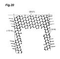
- FIG. 20 is a drawing showing atomic arrangements in (20-21) plane, ( ⁇ 101-8) plane, and ( ⁇ 1018) plane.
- FIG. 1 is a drawing schematically showing a structure of a group-III nitride semiconductor laser device according to an embodiment of the present invention.
- the group-III nitride semiconductor laser device 11 has a gain-guiding type structure, but embodiments of the present invention are not limited to the gain-guiding type structure.
- the group-III nitride semiconductor laser device 11 has a laser structure 13 and an electrode 15 .
- the laser structure 13 includes a support base 17 and a semiconductor region 19 .
- the support base 17 comprises a hexagonal group-III nitride semiconductor and has a semipolar principal surface 17 a and a back surface 17 b .
- the semiconductor region 19 is provided on the semipolar principal surface 17 a of the support base 17 .
- the electrode 15 is provided on the semiconductor region 19 of the laser structure 13 .
- the semiconductor region 19 includes a first cladding layer 21 , a second cladding layer 23 and an active layer 25 .
- the first cladding layer 21 comprises a first conductivity type gallium nitride based semiconductor, e.g., n-type AlGaN, n-type InAlGaN, or the like.
- the second cladding layer 23 comprises a second conductivity type GaN-based semiconductor, e.g., p-type AlGaN, p-type InAlGaN, or the like.
- the active layer 25 is provided between the first cladding layer 21 and the second cladding layer 23 .
- the active layer 25 includes gallium nitride based semiconductor layers, and the gallium nitride based semiconductor layers are, for example, well layers 25 a .
- the active layer 25 includes barrier layers 25 b of a gallium nitride based semiconductor, and the well layers 25 a and the barrier layers 25 b are alternately arranged.
- the well layers 25 a comprise, for example, of InGaN or the like and the barrier layers 25 b , for example, GaN, InGaN, or the like.
- the active layer 25 can include a quantum well structure provided so as to generate light at the wavelength of not less than 360 nm and not more than 600 nm, and making use of the semipolar surface is suitably applicable to generation of light at the wavelength of not less than 430 nm and not more than 550 nm.
- the first cladding layer 21 , the second cladding layer 23 , and the active layer 25 are arranged along an axis NX normal to the semipolar principal surface 17 a .
- the laser structure 13 includes a first fractured face 27 and a second fractured face 29 , which intersect with an m-n plane defined by the normal axis NX and the m-axis of the hexagonal group-III nitride semiconductor.
- an orthogonal coordinate system S and a crystal coordinate system CR are depicted.
- the normal axis NX is directed along a direction of the Z-axis of the orthogonal coordinate system S.
- the semipolar principal surface 17 a extends in parallel with a predetermined plane defined by the X-axis and the Y-axis of the orthogonal coordinate system S.
- a typical c-plane Sc is also depicted.
- the c-axis of the hexagonal group-III nitride semiconductor of the support base 17 tilts at an angle ALPHA with respect to the normal axis NX toward the m-axis of the hexagonal group-III nitride semiconductor.
- the group-III nitride semiconductor laser device 11 further has an insulating film 31 .
- the insulating film 31 covers a surface 19 a of the semiconductor region 19 of the laser structure 13 , and the semiconductor region 19 is located between the insulating film 31 and the support base 17 .
- the support base 17 comprises a hexagonal group-III nitride semiconductor.
- the insulating film 31 has an opening 31 a , and the opening 31 a extends in a direction of an intersecting line LIX between the surface 19 a of the semiconductor region 19 and the foregoing m-n plane, and has, for example, a stripe shape.
- a laser waveguide includes the first cladding layer 21 , the second cladding layer 23 and the active layer 25 , and extends in the direction of the foregoing intersecting line LIX.
- the first fractured face 27 and the second fractured face 29 intersect with the m-n plane defined by the m-axis of the hexagonal group-III nitride semiconductor and the normal axis NX.
- a laser cavity of the group-III nitride semiconductor laser device 11 includes the first and second fractured faces 27 and 29 , and the laser waveguide extends from one of the first fractured face 27 and the second fractured face 29 to the other.
- the laser structure 13 includes a first surface 13 a and a second surface 13 b , and the first surface 13 a is opposite to the second surface 13 b .
- the first and second fractured faces 27 , 29 extend from an edge 13 c of the first surface 13 a to an edge 13 d of the second surface 13 b .
- the first and second fractured faces 27 , 29 are different from the conventional cleaved facets like c-planes, m-planes, or a-planes.
- the group-III nitride semiconductor laser device 11 has the laser cavity enabling a low threshold current.
- the group-III nitride semiconductor laser device 11 includes an n-side optical guide layer 35 and a p-side optical guide layer 37 .
- the n-side optical guide layer 35 includes a first portion 35 a and a second portion 35 b , and the n-side optical guide layer 35 comprises, for example, of GaN, InGaN, or the like.
- the p-side optical guide layer 37 includes a first portion 37 a and a second portion 37 b , and the p-side optical guide layer 37 comprises, for example, of GaN, InGaN, or the like.
- a carrier block layer 39 is provided, for example, between the first portion 37 a and the second portion 37 b .
- Another electrode 41 is provided on the back surface 17 b of the support base 17 , and the electrode 41 covers, for example, the back surface 17 b of the support base 17 .
- the laser structure 13 has, at one end of the first fractured face 27 , a scribed mark SM 1 extending from the edge 13 c of surface 11 a of the group-III nitride semiconductor laser device 11 to the edge 13 d of back surface 11 b of the group-III nitride semiconductor laser device 11 , and has, at the other end of the first fractured face 27 , a scribed mark SM 2 extending from the edge 13 c of the surface 11 a of the group-III nitride semiconductor laser device 11 to the edge 13 d of the back surface 11 b . Furthermore, the laser structure 13 also has scribed marks SM 3 , SM 4 similarly on the second fractured face 29 side.
- the scribed marks SM 1 , SM 2 , SM 3 , SM 4 have a depressed shape extending from the surface 11 a to the back surface 11 b of the group-III nitride semiconductor laser device 11 .
- the scribed marks SM 1 , SM 2 , SM 3 , SM 4 each are provided at ends (ends intersecting with the m-n plane) of the laser structure 13 and extend along a plane defined by the normal axis NX and the a-axis of the hexagonal group-III nitride semiconductor.
- the foregoing ends of the laser structure 13 include one having the first fractured face 27 and one having the second fractured face 29 .
- the first fractured face 27 is a face connecting respective edges 13 e and 13 f of the scribed marks SM 1 and SM 2 and the respective edges 13 c and 13 d of the surface 11 a and the back surface 11 b
- the second fractured face 29 is a face connecting respective edges of the scribed marks SM 3 and SM 4 and the respective edges 13 c and 13 d of the surface 11 a and the back surface 11 b .
- first and second fractured faces 27 , 29 are provided along the scribed mark SM 1 or the like of the depressed shape extending from the surface 11 a to the back surface 11 b of the group-III nitride semiconductor laser device 11 as described above, the fractured faces are expected to have sufficient perpendicularity and flatness, and the first and second fractured faces 27 , 29 can have the perpendicularity and flatness enough for laser cavity mirrors.
- FIG. 2 is a drawing showing a band structure in the active layer in the group-III nitride semiconductor laser device.
- FIG. 3 is a drawing showing polarization of emission from the active layer 25 of the group-III nitride semiconductor laser device 11 .
- FIG. 4 is a schematic cross sectional view taken along a plane defined by the c-axis and the m-axis. With reference to Part (a) of FIG. 2 , three possible transitions between the conduction band and valence bands in the vicinity of ⁇ point of the band structure BAND are shown. The energy difference between band A and band B is relatively small.
- An emission by transition Ea between the conduction band and band A is polarized in the a-axis direction
- an emission by transition Eb between the conduction band and band B is polarized in a direction of the c-axis projected onto the principal surface.
- a threshold of transition Ea is smaller than a threshold of transition Eb.
- the light in the LED mode includes a polarization component I 1 in the direction of the a-axis of the hexagonal group-III nitride semiconductor, and a polarization component I 2 in the direction of the projected c-axis of the hexagonal group-III nitride semiconductor onto the principal surface, and the polarization component I 1 is larger than the polarization component I 2 .
- Degree of polarization ⁇ is defined by (I 1 ⁇ I 2 )/(I 1 +I 2 ).
- the laser cavity of the group-III nitride semiconductor laser device 11 enables the device to emit a laser beam in the mode that has large emission intensity in the LED mode.
- the device may be further provided with dielectric multilayer film 43 a , 43 b on at least one of the first and second fractured faces 27 , 29 or on the respective faces.
- dielectric multilayer film 43 a , 43 b on at least one of the first and second fractured faces 27 , 29 or on the respective faces.
- An end face coating is also applicable to the first and second fractured faces 27 , 29 . The end face coating allows adjustment of their reflectance.
- the laser light L from the active layer 25 is polarized in the direction of the a-axis of the hexagonal group-III nitride semiconductor.
- this group-III nitride semiconductor laser device 11 a band transition allowing for implementation of a low threshold current has polarized nature.
- the first and second fractured faces 27 , 29 for the laser cavity are different from the conventional cleaved facets like c-planes, m-planes, or a-planes. But, the first and second fractured faces 27 , 29 have flatness and perpendicularity as mirrors for lasing cavity.
- an end face 17 c of the support base 17 and an end face 19 c of the semiconductor region 19 are exposed in each of the first and second fractured faces 27 and 29 , and the end face 17 c and the end face 19 c are covered with the dielectric multilayer film 43 a .
- An angle BETA between an m-axis vector MA of the active layer 25 and a vector NA normal to the end face 17 c of the support base 17 , and an end face 25 c in the active layer 25 has a component (BETA) 1 defined on a first plane S 1 , which is defined by the c-axis and m-axis of the group-III nitride semiconductor, and a component (BETA) 2 defined on a second plane S 2 (which is not shown but referred to as “S 2 ” for easier understanding), which is perpendicular to the first plane S 1 (which is not shown but referred to as “S 1 ” for easier understanding) and the normal axis NX.
- the component (BETA) 1 is preferably in a range of not less than (ALPHA ⁇ 5)° and not more than (ALPHA+5)° in the first plane S 1 defined by the c-axis and m-axis of the group-III nitride semiconductor.
- This angular range is shown as an angle between a typical m-plane S M and a reference plane F A in FIG. 4 .
- the typical m-plane S M is depicted from the inside to the outside of the laser structure in FIG. 4 , for easier understanding.
- the reference plane F A extends along the end face 25 c of the active layer 25 .
- This group-III nitride semiconductor laser device 11 has the end faces in which the angle BETA taken from one of the c-axis and the m-axis to the other satisfies the aforementioned perpendicularity.
- the component (BETA) 2 is preferably in a range of not less than ⁇ 5° and not more than +5° on the second plane S 2 .
- BETA 2 (BETA) 1 2 +(BETA) 2 2 .
- the end faces (the first and second fractured faces 27 and 29 ) of the group-III nitride semiconductor laser device 11 satisfy the aforementioned perpendicularity as to the in-plane angle defined in the plane that is perpendicular to the normal axis NX to the semipolar principal surface 17 a.
- the thickness DSUB of the support base 17 is preferably not less than 50 ⁇ m and not more than 150 ⁇ m.
- the support base 17 of the group-III nitride semiconductor laser device 11 has this thickness, it becomes easier to form scribed through-holes (cf. below-described scribed through-holes 65 a shown in FIG. 6 ) corresponding to the scribed marks SM, in a substrate product (below-described substrate product SP) including the group-III nitride semiconductor laser device 11 .
- end faces (fractured faces) obtained through the use of the scribed through-holes are applicable as good laser cavity mirrors with sufficient perpendicularity and flatness. Therefore, the first and second fractured faces 27 , 29 of the group-III nitride semiconductor laser device 11 can serve as good laser cavity mirrors.
- the angle ALPHA between the normal axis NX and the c-axis of the hexagonal group-III nitride semiconductor is preferably not less than 45° and preferably not more than 80°, and the angle ALPHA is preferably not less than 100° and preferably not more than 135°.
- the angle is in a range of less than 45° and in a range of more than 135°, the end faces made by press are highly likely to be comprised of m-planes.
- the angle is in a range of more than 80° and less than 100°, it could result in failing to achieve desired flatness and perpendicularity.
- the angle ALPHA between the normal axis NX and the c-axis of the hexagonal group-III nitride semiconductor is not less than 63° and not more than 80°. Furthermore, the angle ALPHA is particularly preferably not less than 100° and not more than 117°. When the angle is in a range of less than 63° and in a range of more than 117°, an m-plane can be formed in part of an end face made by press. When the angle is in a range of more than 80° and less than 100°, it could result in failing to achieve desired flatness and perpendicularity.
- the semipolar principal surface 17 a can be any one of ⁇ 20-21 ⁇ plane, ⁇ 10-11 ⁇ plane, ⁇ 20-2-1 ⁇ plane and ⁇ 10-1-1 ⁇ plane. Furthermore, a surface with a slight tilt in a range of not less than ⁇ 4° and not more than +4° with respect to these planes may also be applied as the principal surface.
- the first and second end faces (the first and second fractured faces 27 and 29 ) with flatness and perpendicularity enough to construct the laser cavity of the group-III nitride semiconductor laser device 11 . Furthermore, end faces with sufficient flatness and perpendicularity are obtained in an angular range across these typical plane orientations.
- the stacking fault density of the support base 17 can be not more than 1 ⁇ 10 4 cm ⁇ 1 . Since the stacking fault density is not more than 1 ⁇ 10 4 cm ⁇ 1 , the flatness and/or perpendicularity of the fractured faces is less likely to be disturbed for a certain accidental reason.
- the support base 17 can comprise any one of GaN, AlN, AlGaN, InGaN, and InAlGaN. When the substrate of any one of these GaN-based semiconductors is used, the end faces (the first and second fractured faces 27 and 29 ) applicable to the cavity can be obtained.
- FIG. 5 is a drawing showing major steps in a method of fabricating the group-III nitride semiconductor laser device according to the present embodiment.
- a substrate 51 is shown.
- the substrate 51 is prepared for fabrication of the group-III nitride semiconductor laser device.
- the c-axis (vector VC) of the hexagonal group-III nitride semiconductor of the substrate 51 tilts at an angle ALPHA with respect to the normal axis NX toward the m-axis (vector VM) of the hexagonal group-III nitride semiconductor.
- the substrate 51 has a semipolar principal surface 51 a of the hexagonal group-III nitride semiconductor.
- step S 102 a substrate product SP is formed.
- the substrate product SP is depicted as a member of a nearly disklike shape, but the shape of the substrate product SP is not limited thereto.
- step S 103 is first performed to form a laser structure 55 .
- the laser structure 55 includes a semiconductor region 53 and the substrate 51 , and in step S 103 , the semiconductor region 53 is grown on the semipolar principal surface 51 a .
- a first conductivity type GaN-based semiconductor region 57 , a light emitting layer 59 , and a second conductivity type GaN-based semiconductor region 61 are grown sequentially on the semipolar principal surface 51 a .
- the GaN-based semiconductor region 57 can include, for example, an n-type cladding layer and the GaN-based semiconductor region 61 can include, for example, a p-type cladding layer.
- the light emitting layer 59 is provided between the GaN-based semiconductor region 57 and the GaN-based semiconductor region 61 , and can include an active layer, optical guide layers, an electron block layer, and so on.
- the GaN-based semiconductor region 57 , the light emitting layer 59 , and the second conductivity type GaN-based semiconductor region 61 are arranged in the direction of the normal axis NX to the semipolar principal surface 51 a . These semiconductor layers are epitaxially grown thereon.
- the surface of the semiconductor region 53 is covered with an insulating film 54 .
- the insulating film 54 comprises, for example, of silicon oxide.
- the insulating film 54 has an opening 54 a .
- the opening 54 a has, for example, a stripe shape.
- Step S 104 is carried out to form an anode electrode 58 a and a cathode electrode 58 b on the laser structure 55 .
- the back surface of the substrate used in crystal growth is polished to form a substrate product SP in desired thickness DSUB.
- the anode electrode 58 a is formed on the semiconductor region 53
- the cathode electrode 58 b is formed on the back surface (polished surface) 51 b of the substrate 51 .
- the anode electrode 58 a extends in the X-axis direction
- the cathode electrode 58 b covers the entire area of the back surface 51 b .
- the substrate product SP is obtained.
- the substrate product SP includes a first surface 63 a , and a second surface 63 b located opposite thereto.
- the semiconductor region 53 is located between the first surface 63 a and the substrate 51 .
- Step S 105 is to scribe the first surface 63 a of the substrate product SP, as shown in Part (b) of FIG. 6 .
- This scribing is carried out using a laser scriber 10 a .
- the scribing results in forming a plurality of scribed through-holes 65 a .
- Part (b) of FIG. 6 several scribed through-holes are already formed, and formation of a scribed through-hole 65 b is in progress with a laser beam LB.
- the scribed through-holes 65 a and the like are through-holes penetrating the substrate product SP from the first surface 63 a to the second surface 63 b thereof, and have a shape extending in the a-axis direction of the hexagonal group-III nitride semiconductor when viewed from the first surface 63 a (or the second surface 63 b ).
- the width of the scribed through-holes 65 a and the like in the a-axis direction of the hexagonal group-III nitride semiconductor is larger than the width thereof in the direction perpendicular to the a-axis direction of the hexagonal group-III nitride semiconductor.
- the width of the scribed through-holes 65 a and the like in the a-axis direction of the hexagonal group-III nitride semiconductor can be, for example, not less than 50 ⁇ m and not more than 300 ⁇ m, and the width of the scribed through-holes 65 a and the like in the direction perpendicular to the a-axis direction of the hexagonal group-III nitride semiconductor can be, for example, not less than 5 ⁇ m and not more than 15 ⁇ m.
- the plurality of scribed through-holes 65 a and the like are formed, for example, at the pitch of about 400 ⁇ m along the a-axis direction of the hexagonal group-III nitride semiconductor.
- a plurality of lines each including a plurality of scribed through-holes 65 a formed along the a-axis direction of the hexagonal group-III nitride semiconductor are formed at a pitch of an approximately equal interval in the substrate product SP, along a plane defined by the c-axis and m-axis of the hexagonal group-III nitride semiconductor.
- the scribed through-holes 65 a and the like become the scribed mark SM 1 and others of the group-III nitride semiconductor laser device 11 .
- the length of the scribed through-holes 65 a is shorter than the length of an intersecting line MS between the first surface 63 a and an a-n plane defined by the normal axis NX and the a-axis of the hexagonal group-III nitride semiconductor, and the laser beam LB is applied to a part of the intersecting line MS.
- the scribed through-holes 65 a can be formed, for example, in an edge of the substrate product SP.
- step S 106 is carried out to implement breakup of the substrate product SP by press against the second surface 63 b of the substrate product SP, thereby forming a substrate product SP 1 and a laser bar LB 1 .
- the press is carried out with a breaking device, such as, a blade 69 .
- This breaking (primary break) for forming the laser bar LB 1 is carried on along the y-axis direction.
- the blade 69 includes an edge 69 a extending in one direction, and at least two blade faces 69 b and 69 c that are formed to define the edge 69 a .
- the pressing onto the substrate product SP 1 is carried out on a support device 71 .
- the support device 71 includes a support table 71 a and a recess 71 b , and the recess 71 b extends in one direction.
- the recess 71 b is formed in the support table 71 a .
- the orientation and position of the scribed through-hole 65 a of the substrate product SP 1 are aligned with the extending direction of the recess 71 b of the support device 71 to position the substrate product SP 1 to the recess 71 b on the support device 71 .
- the orientation of the edge of the breaking device is aligned with the extending direction of the recess 71 b , and the edge of the breaking device is pressed against the substrate product SP 1 from a direction intersecting with the second surface 63 b .
- the intersecting direction is preferably an approximately vertical direction to the second surface 63 b .
- This implements the breakup of the substrate product SP to form the substrate product SP 1 and laser bar LB 1 .
- the press results in forming the laser bar LB 1 with first and second end faces 67 a and 67 b , and these end faces 67 a and 67 b have perpendicularity and flatness enough to make at least a part of the light emitting layer applicable to mirrors for the laser cavity of the semiconductor laser.
- the laser bar LB 1 thus formed has the first and second end faces 67 a , 67 b formed by the aforementioned breakup, and each of the end faces 67 a , 67 b extends from the first surface 63 a to the second surface 63 b .
- the end faces 67 a , 67 b form the laser cavity of the group-III nitride semiconductor laser device, and intersect with the XZ plane.
- This XZ plane corresponds to the m-n plane defined by the normal axis NX and the m-axis of the hexagonal group-III nitride semiconductor.
- the first surface 63 a of the substrate product SP is scribed in the direction of the a-axis of the hexagonal group-III nitride semiconductor, and thereafter the breakup of the substrate product SP is carried out by press against the second surface 63 b of the substrate product SP, thereby forming the new substrate product SP 1 and the laser bar LB 1 .
- This method allows the formation of the first and second end faces 67 a , 67 b , which intersect with the m-n plane, in the laser bar LB 1 .
- This end face forming method provides the first and second end faces 67 a , 67 b with flatness and perpendicularity enough to construct the laser cavity of the group-III nitride semiconductor laser device.
- the laser waveguide thus formed extends in the direction of inclination of the c-axis of the hexagonal group-III nitride.
- the end faces of the laser cavity mirror allowing for provision of this laser waveguide are formed without use of dry-etching.
- This method involves the fracturing of the substrate product SP 1 , thereby forming the new substrate product SP 1 and the laser bar LB 1 .
- Step S 107 the breakup is repeatedly carried out by press to produce a number of laser bars. This fracture propagates along the scribed through-holes 65 a shorter than a fracture line BREAK of the laser bar LB 1 .
- Step S 108 dielectric multilayer films is formed on the end faces 67 a , 67 b of the laser bar LB 1 to form a laser bar product.
- Step S 109 this laser bar product is separated into individual semiconductor laser dies (secondary break).
- the angle ALPHA can be in a range of not less than 45° and not more than 80° and in a range of not less than 100° and not more than 135°.
- the angle is in a range of less than 45° and in a range of more than 135°, the end face made by press becomes highly likely to be comprised of an m-plane.
- the angle is in a range of more than 80° and less than 100°, it may result in failing to achieve desired flatness and perpendicularity.
- the angle ALPHA can be in a range of not less than 63° and not more than 80° and in a range of not less than 100° and not more than 117°.
- an m-plane can be formed in part of an end face formed by press.
- the semipolar principal surface 51 a can be any one of ⁇ 20-21 ⁇ plane, ⁇ 10-11 ⁇ plane, ⁇ 20-2-1 ⁇ plane, and ⁇ 10-1-1 ⁇ plane.
- a surface slightly tilted in a range of not less than ⁇ 4° and not more than +4° from the above planes is also used as the principal surface.
- the substrate 51 can be made of any one of GaN, AlN, AlGaN, InGaN, and InAlGaN. When any one of these GaN-based semiconductors is used for the substrate, it is feasible to obtain the end faces applicable to the laser cavity.
- the substrate 51 is preferably made of GaN.
- the semiconductor substrate used in crystal growth can be one subjected to processing such as slicing or grinding so that the substrate thickness becomes not less than 50 ⁇ m and not more than 150 ⁇ m, and having the second surface 63 b of a processed surface formed by polishing.
- this substrate thickness it becomes easier to form the scribed through-holes 65 a , and the end faces 67 a , 67 b can be formed in good yield, with flatness and perpendicularity enough to construct the laser cavity of the group-III nitride semiconductor laser device, or without ion damage.
- the angle BETA explained with reference to FIG. 3 can be also defined in the laser bar LB 1 .
- the component (BETA) 1 of the angle BETA is preferably in a range of not less than (ALPHA ⁇ 5)° and not more than (ALPHA+5)° on a first plane (plane corresponding to the first plane S 1 in the description with reference to FIG. 3 ) defined by the c-axis and m-axis of the group-III nitride semiconductor.
- the end faces 67 a , 67 b of the laser bar LB 1 satisfy the aforementioned perpendicularity as to the angle component of the angle BETA taken from one of the c-axis and the m-axis to the other.
- the component (BETA) 2 of the angle BETA is preferably in a range of not less than ⁇ 5° and not more than +5° on a second plane (plane corresponding to the second plane S 2 shown in FIG. 3 ).
- These end faces 67 a , 67 b of the laser bar LB 1 also satisfy the aforementioned perpendicularity as to the angle component of the angle BETA defined on the plane perpendicular to the normal axis NX to the semipolar principal surface 51 a.
- the end faces 67 a , 67 b are formed by break by press against the plurality of GaN-based semiconductor layers epitaxially grown on the semipolar principal surface 51 a . Since they are epitaxial films on the semipolar principal surface 51 a , each of the end faces 67 a , 67 b are not cleaved facets each having a low plane index like c-planes, m-planes, or a-planes which have been used heretofore for the conventional laser cavity mirrors. However, through the break of the stack of epitaxial films on the semipolar principal surface 51 a , the end faces 67 a , 67 b have flatness and perpendicularity applicable as laser cavity mirrors.
- a laser diode shown in FIG. 7 is grown by organometallic vapor phase epitaxy as described below.
- the raw materials used are as follows: trimethyl gallium (TMGa); trimethyl aluminum (TMAl); trimethyl indium (TMIn); ammonia (NH 3 ); and silane (SiH 4 ).
- TMGa trimethyl gallium
- TMAl trimethyl aluminum
- TMIn trimethyl indium
- NH 3 ammonia
- SiH 4 silane
- a GaN substrate is prepared as the substrate 71 , and the GaN substrate is cut with a wafer slicing apparatus at an angle in a range of 0° to 90° to the m-axis from a (0001) GaN ingot thickly grown by HVPE, in such a manner that the angle ALPHA of the c-axis tilted toward the m-axis has a desired off angle in a range of 0° to 90°.
- the resultant substrate is prepared as a GaN substrate having a ⁇ 20-21 ⁇ -plane.
- the substrate is observed by the cathodoluminescence method in order to estimate the stacking fault density of the substrate.
- the cathodoluminescence an emission process of carriers excited by an electron beam is observed and in a stacking fault, non-radiative recombination of carriers occurs in the vicinity thereof, so that the stacking fault is expected be observed as a dark line.
- the stacking fault density is defined as a density (line density) per unit length of dark lines observed.
- the cathodoluminescence method of nondestructive measurement is applied herein in order to estimate the stacking fault density, but it is also possible to use destructive measurement, such as a transmission electron microscope.
- a defect extending in the m-axis direction from the substrate toward the sample surface indicates a stacking fault contained in the support base, and the line density of stacking faults can be determined in the same manner as in the cathodoluminescence method.
- the above substrate 71 is placed on a susceptor in a reactor, and the epitaxial layers are grown in the following growth procedure.
- an n-type GaN 72 is grown thereon and its the thickness is 1000 nm.
- an n-type InAlGaN cladding layer 73 is grown thereon and its thickness is 1200 nm.
- an n-type GaN guide layer 74 a and an undoped InGaN guide layer 74 b are grown, their thickness are 200 nm and 65 nm, respectively, and then a three-cycle MQW 75 constituted by GaN 15 nm thick/InGaN 3 nm thick is grown thereon.
- a p-type InGaN guide layer 76 a of the thickness of 65 nm is grown thereon, and a p-type AlGaN block layer 77 a of the thickness of 20 nm, and a p-type InGaN guide layer 76 b of the thickness of 200 nm.
- a p-type InAlGaN cladding layer 77 b is grown thereon, and its thickness is 400 nm.
- a p-type GaN contact layer 78 is grown thereon and its thickness is 50 nm.
- An insulating film 79 of SiO 2 is deposited on the contact layer 78 and then photolithography and wet etching processes are applied to form a stripe window having the width of 10 ⁇ m in the insulating film 79 .
- a contact window is formed along a stripe direction which is an M-direction (direction of the contact window extending along the predetermined plane defined by the c-axis and the m-axis).
- a p-side electrode 80 a of Ni/Au and a pad electrode of Ti/Al are made by vapor deposition.
- the back surface of the GaN substrate (GaN wafer) is polished to 80 ⁇ m (or 60 ⁇ m) using diamond slurry to produce a substrate product with the mirror-polished back surface.
- the thickness of the thus formed substrate product is measured with a contact film thickness meter.
- the measurement of substrate thickness may also be carried out with a microscope from the observation of a cross section of a prepared sample.
- the microscope applicable herein can be an optical microscope or a scanning electron microscope.
- An n-side electrode 80 b of Ti/Al/Ti/Au is formed by vapor deposition on the back surface (polished surface) of the GaN substrate (GaN wafer).
- the laser cavity mirrors for laser stripes are produced with a laser scriber that uses the YAG laser at the wavelength of 355 nm.
- the laser chip yield can be improved as compared with break implemented using a diamond scriber.
- substrate thickness laser output laser scanning speed ( ⁇ m), (mW), (mm/s); method (A) 80, 250, 1; method (B) 60, 250, 1
- scribed grooves SL 1 , SL 2 are formed in the first surface 63 a of the substrate product SP so as not to reach the second surface 63 b .
- the scribed grooves SL 1 , SL 2 are grooves formed in the first surface 63 a without reaching the second surface 63 b of the substrate product SP.
- a group-III nitride semiconductor laser device with the scribed grooves SL 1 , SL 2 will be particularly referred to as group-III nitride semiconductor laser device 111 .
- the scribed through-holes and the scribed grooves are formed at the pitch of 400 ⁇ m by applying a laser beam directly onto the epitaxially grown surface through opening portions of the insulating film on the substrate.
- the laser cavity length is 600 ⁇ m.
- the scribed through-holes thus formed have, for example, the length of about 200 ⁇ m and the width of about 12 ⁇ m, and the scribed grooves have, for example, the length of about 200 ⁇ m, the width of about 8 ⁇ m, and the depth of about 40 ⁇ m.
- the fractured faces made by break are observed with a scanning electron microscope, and no prominent unevenness is observed. From this result, the flatness (magnitude of unevenness) of the fractured faces can be not more than 20 nm. Furthermore, the perpendicularity of the fractured faces to the surface of the sample can be within a range of ⁇ 5°.
- the end faces of the laser bar are coated with a dielectric multilayer film by vacuum vapor deposition.
- the dielectric multilayer film is composed of an alternate stack of SiO 2 and TiO 2 . Each thickness thereof is adjusted in a range of 50 to 100 nm and is designed so that the center wavelength of reflectance falls within a range of 500 to 530 nm.
- the reflecting surface on one side has an alternate stack of ten cycles and a designed value of reflectance of about 95%, and the reflecting surface on the other side has an alternate stack of six cycles and a designed value of reflectance of about 80%.
- the devices thus formed are energized to make their evaluation at room temperature.
- a pulsed power source is used as a power supply for the energization, and supplies pulses with the pulse width of 500 ns and the duty ratio of 0.1%, and the energization is implemented through probing needles that are in contact with the surface electrodes.
- an emission from the end face of the laser bar is detected with a photodiode to obtain a current-light output characteristic (I-L characteristic).
- I-L characteristic current-light output characteristic
- the emission from the end face of the laser bar is supplied through an optical fiber to a spectrum analyzer of a detector to measure a spectrum thereof.
- the emission from the laser bar is made to pass through a polarizing plate by rotation, thereby determining the polarization state.
- an optical fiber is aligned to the front surface side of the laser bar to measure optical emission from the front surface.
- the polarization in the laser beam is measured for every laser device, and it is found that the laser beam is polarized in the a-axis direction.
- the laser wavelength is in a range of 500-530 nm.
- FIG. 8 is a schematic diagram of a substrate obtained by forming the scribed grooves in the substrate product SP by the method (C).
- x-directional scribed grooves (scribed grooves SL 2 ) for secondary break are also formed in addition to y-directional scribed grooves (scribed grooves SL 1 ) for primary break, but in a practical process the scribed grooves SL 2 for secondary break are formed after the primary break.
- FIG. 9 shows the observation result in observation with an optical microscope of an epitaxially grown surface of a semipolar-plane LD (group-III nitride semiconductor laser device 111 ) fabricated as a chip through the primary and secondary breaks.
- the break proceeding direction is the y-direction.
- a fissure by break (denoted by symbol D 1 in the drawing) develops so as to turn from the direction (y-direction) perpendicular to the waveguide, to the direction of the c-axis (projected direction D 2 of the c-axis on the epitaxially grown surface, which corresponds to the ⁇ x direction).
- the laser cavity mirrors perpendicular to the waveguide are not obtained, and it is expected that they will cause decrease in lasing yield and increase in lasing threshold current.
- the quality of the laser cavity mirrors can become unstable by the technology of forming the scribed grooves SL 1 , SL 2 by the method (C).
- FIG. 10 shows the result of observation of an end face (z-x cross section) of this semipolar-plane LD (group-III nitride semiconductor laser device 111 ).
- Part (a) of FIG. 10 is a view of the epitaxially grown surface of the group-III nitride semiconductor laser device 111
- Part (b) of FIG. 10 is a view of a side surface of the group-III nitride semiconductor laser device 111 in a region D 3 shown in Part (a) of FIG. 10 . It is seen from FIG.
- FIG. 11 shows the result of observation to observe how appearances of the end face in the depth direction vary with development of a fissure in the direction (y-direction) perpendicular to the waveguide.
- the end face is composed of two planes, the plane relatively perpendicular to the epitaxially grown surface, which is made by scribing, and the c-plane appearing below the scribed groove SL 1 , and has an edge as an intersecting line between the two planes.
- the fissure develops in the y-direction to reach a region where no scribed groove is formed (200 ⁇ m ⁇ y ⁇ 400 ⁇ m in FIG. 11 )
- the aforementioned two planes constituting the end face gradually come to connect smoothly so as to eliminate the edge.
- the end face becomes a curved surface.
- the inventor interpreted the mechanism of development of fissure as shown in FIG. 12 , based on the result shown in FIG. 11 . According to Inventor's knowledge, it is found that the press with the blade makes a straight edge on the surface against which the blade is urged during the break (on the substrate back surface D 8 side). As described above, the c-plane appears on the back surface D 8 side (regions indicated by symbol D 6 in the drawing) below the scribed grooves.
- the cause of the failure in stably obtaining the laser cavity mirrors perpendicular to the waveguide in the case using the aforementioned method (C) is highly likely to be the c-plane appearing on the substrate back side below the scribed grooves SL 1 .
- the inventor consider that the laser cavity mirrors perpendicular to the waveguide could be stably obtained by suppressing the appearance of the c-plane on the substrate back side below the scribed grooves SL 1 , and discovered the aforementioned methods (A), (B) of forming the through-holes (scribed through-holes 65 a and the like) penetrating the substrate product from the epitaxially grown surface to the substrate back surface with the laser scriber and performing the break.
- Part (a) of FIG. 13 and Part (b) of FIG. 13 optical microscope photographs of a sample (laser bar LB 1 or the like) obtained by the method (A) are shown.
- Part (a) of FIG. 13 the observation result from the epitaxially grown surface is shown.
- Part (b) of FIG. 13 the observation result from the end face is shown.
- the angular deviation of the laser cavity mirror from the direction perpendicular to the waveguide, as observed in FIG. 9 is not recognized. It is clear from Part (b) of FIG. 13 that through-holes are surely formed in this case.
- Part (a) of FIG. 14 shows the observation result of an appearance of an end face near the waveguide of this sample (laser bar LB 1 or the like). The end face is virtually perpendicular to the epitaxially grown surface, and is different from the conventional cleaved facets. For finding candidates for this end face, plane indices to make an angle near 90° to the (20-21) plane are determined by calculation. With reference to Part (b) of FIG. 14 , the angles and plane indices below have angles near 90° to the (20-21) plane.
- FIG. 15 shows the results of measurement of angular deviation GAMMA of the end face from the line in which the scribed through-holes (scribed grooves) are arrayed (the y-axis in FIG. 12 ), based on the observation results from the epitaxially grown surface of the samples (laser bars LB 1 or the like) obtained by the methods (A) to (C).
- FIG. 15 shows the results of measurement of angular deviation GAMMA of the end face from the line in which the scribed through-holes (scribed grooves) are arrayed (the y-axis in FIG. 12 ), based on the observation results from the epitaxially grown surface of the samples (laser bars LB 1 or the like) obtained by the methods (A) to (C).
- columns NU 11 , NU 12 , NU 13 represent the results in the case where the scribed through-holes 65 a are formed by the method (A); columns NU 21 , NU 22 represent the results in the case where the scribed through-holes 65 a are formed by the method (B); columns NU 31 , NU 32 , NU 33 represent the results in the case where the scribed grooves SL 1 or the like are formed by the method (C).
- FIG. 15 It is confirmed by FIG. 15 that the angular deviation GAMMA is reduced in the samples (laser bars LB 1 or the like) obtained by the methods of forming the scribed through-holes 65 a or the like (method (A) and method (B)).
- the data shown in FIG. 15 is as described below.
- Averages and standard deviations of the angular deviations GAMMA in the respective methods (A) to (C) are as follows.
- the relation of tilt angle of the c-axis toward the m-axis of GaN substrate (support base 17 ) of the group-III nitride semiconductor laser device 11 versus lasing yield is measured using the method (A).
- the result of this measurement is shown in FIG. 16 .
- the lasing yield is defined as (the number of laser chips)/(the number of measured chips).
- the measurement result shown in FIG. 16 is obtained using the GaN substrate with the stacking fault density of not more than 1 ⁇ 10 4 (cm ⁇ 1 ). It is seen from FIG. 16 that the lasing yield is extremely low with the off angles of not more than 45°.
- the optimum off angle range of the GaN substrate (support base 17 ) is not less than 63° and not more than 80°. The same result is also obtained in a range of not less than 100° and not more than 117°, which is an angle range to provide crystallographically equivalent end faces.
- the data shown in FIG. 16 is as described below.
- the relation between stacking fault density and lasing yield is investigated using the method (A), and the result obtained is shown in FIG. 17 .
- the definition of lasing yield is the same as above. It is seen from FIG. 17 that the lasing yield suddenly decreases with the stacking fault density of the GaN substrate (support base 17 ) over 1 ⁇ 10 4 (cm ⁇ 1 ). When the end face state is observed with an optical microscope, it is found that with samples having the decreased lasing yield, the unevenness of the end face is significant, and no flat end face is obtained. A conceivable reason for it is that there is a difference in easiness of fracture because of the existence of stacking faults.
- the stacking fault density in the GaN substrate (support base 17 ) needs to be not more than 1 ⁇ 10 4 (cm ⁇ 1 ).
- the scribed through-holes 65 a or the like reaching the back surface of the substrate are formed by applying the laser to the epitaxially grown surface (first surface 63 a of substrate product SP) during the scribing, whereas it is confirmed with the optical microscope that damages and debris of the epitaxially grown surface are decreased by forming the scribed through-holes 65 a or the like reaching the epitaxially grown surface by applying the laser to the back surface of the substrate (the second surface 63 b of the substrate product SP).
- This method can improve the yield of LD (group-III nitride semiconductor laser device 11 ).
- the data shown in FIG. 17 is as described below.
- stacking fault density (cm ⁇ 1 ), yield; 500, 95; 1000, 91; 4000, 72; 8000, 64; 10000, 18; 50000, 3
- FIG. 18 is a drawing showing atomic arrangements in the (20-21) plane, ( ⁇ 101-6) plane, and ( ⁇ 1016) plane.
- FIG. 19 is a drawing showing atomic arrangements in the (20-21) plane, ( ⁇ 101-7) plane, and ( ⁇ 1017) plane.
- FIG. 20 is a drawing showing atomic arrangements in the (20-21) plane, ( ⁇ 101-8) plane, and ( ⁇ 1018) plane.
- local atom arrangements indicated by arrows show configurations of atoms with charge neutrality, and electrically neutral arrangements of atoms appear periodically. The reason why the near-vertical faces with respect to the grown surface are obtained can be that creation of fractured faces is considered to be relatively stable because of the periodic appearance of the neutral atomic configurations in terms of charge.
- the angle ALPHA can be in a range of not less than 45° and not more than 80° or in a range of not less than 100° and not more than 135°. In order to improve the laser chip yield, the angle ALPHA can be in a range of not less than 63° and not more than 80° or in a range of not less than 100° and not more than 117°.
- the typical semipolar principal surface can be any one of ⁇ 20-21 ⁇ plane, ⁇ 10-11 ⁇ plane, ⁇ 20-2-1 ⁇ plane, and ⁇ 10-1-1 ⁇ plane. Furthermore, the principal surface can be a slight tilt surface from these semipolar surfaces.
- the semipolar principal surface can be a slight tilt surface off in a range of not less than ⁇ 4° and not more than +4° toward the m-plane with respect to any one of ⁇ 20-21 ⁇ plane, ⁇ 10-11 ⁇ plane, ⁇ 20-2-1 ⁇ plane, and ⁇ 10-1-1 ⁇ plane.
- the embodiments provide the group-III nitride semiconductor laser device with the laser cavity enabling the low threshold current, on the semipolar surface of the support base the c-axis of the hexagonal group-III nitride of which tilts toward the m-axis. And the embodiments provide the method for fabricating this group-III nitride semiconductor laser device.
Landscapes
- Physics & Mathematics (AREA)
- Optics & Photonics (AREA)
- Condensed Matter Physics & Semiconductors (AREA)
- General Physics & Mathematics (AREA)
- Electromagnetism (AREA)
- Chemical & Material Sciences (AREA)
- Engineering & Computer Science (AREA)
- Nanotechnology (AREA)
- Life Sciences & Earth Sciences (AREA)
- Biophysics (AREA)
- Crystallography & Structural Chemistry (AREA)
- Semiconductor Lasers (AREA)
Priority Applications (1)
| Application Number | Priority Date | Filing Date | Title |
|---|---|---|---|
| US13/209,101 US8213475B2 (en) | 2010-01-18 | 2011-08-12 | Group-III nitride semiconductor laser device, and method for fabricating group-III nitride semiconductor laser device |
Applications Claiming Priority (3)
| Application Number | Priority Date | Filing Date | Title |
|---|---|---|---|
| JP2010008414A JP4793494B2 (ja) | 2010-01-18 | 2010-01-18 | Iii族窒化物半導体レーザ素子を作製する方法 |
| JP2010-008414 | 2010-01-18 | ||
| JPP2010-008414 | 2010-01-18 |
Related Child Applications (1)
| Application Number | Title | Priority Date | Filing Date |
|---|---|---|---|
| US13/209,101 Division US8213475B2 (en) | 2010-01-18 | 2011-08-12 | Group-III nitride semiconductor laser device, and method for fabricating group-III nitride semiconductor laser device |
Publications (2)
| Publication Number | Publication Date |
|---|---|
| US20110176569A1 US20110176569A1 (en) | 2011-07-21 |
| US8071405B2 true US8071405B2 (en) | 2011-12-06 |
Family
ID=44277557
Family Applications (2)
| Application Number | Title | Priority Date | Filing Date |
|---|---|---|---|
| US12/836,281 Expired - Fee Related US8071405B2 (en) | 2010-01-18 | 2010-07-14 | Group-III nitride semiconductor laser device, and method for fabricating group-III nitride semiconductor laser device |
| US13/209,101 Expired - Fee Related US8213475B2 (en) | 2010-01-18 | 2011-08-12 | Group-III nitride semiconductor laser device, and method for fabricating group-III nitride semiconductor laser device |
Family Applications After (1)
| Application Number | Title | Priority Date | Filing Date |
|---|---|---|---|
| US13/209,101 Expired - Fee Related US8213475B2 (en) | 2010-01-18 | 2011-08-12 | Group-III nitride semiconductor laser device, and method for fabricating group-III nitride semiconductor laser device |
Country Status (7)
| Country | Link |
|---|---|
| US (2) | US8071405B2 (ja) |
| EP (1) | EP2528175A1 (ja) |
| JP (1) | JP4793494B2 (ja) |
| KR (1) | KR101285049B1 (ja) |
| CN (1) | CN102341977B (ja) |
| TW (1) | TW201134039A (ja) |
| WO (1) | WO2011086756A1 (ja) |
Cited By (7)
| Publication number | Priority date | Publication date | Assignee | Title |
|---|---|---|---|---|
| US20110058585A1 (en) * | 2009-09-10 | 2011-03-10 | Sumitomo Electric Industries, Ltd. | Group-iii nitride semiconductor laser device, and method of fabricating group-iii nitride semiconductor laser device |
| US20110075694A1 (en) * | 2009-09-30 | 2011-03-31 | Sumitomo Electric Industries, Ltd. | III-Nitride semiconductor laser device, and method of fabricating the III-Nitride semiconductor laser device |
| US20110158277A1 (en) * | 2009-12-25 | 2011-06-30 | Sumitomo Electric Industries, Ltd. | Group-iii nitride semiconductor laser device, method of fabricating group-iii nitride semiconductor laser device, and epitaxial substrate |
| US20110164637A1 (en) * | 2009-06-17 | 2011-07-07 | Sumitomo Electric Industries, Ltd. | Group-iii nitride semiconductor laser device, and method for fabricating group-iii nitride semiconductor laser device |
| US20110228804A1 (en) * | 2010-01-18 | 2011-09-22 | Sumitomo Electric Industries, Ltd. | Group-iii nitride semiconductor laser device, and method for fabricating group-iii nitride semiconductor laser device |
| US20120100654A1 (en) * | 2009-12-25 | 2012-04-26 | Sumitomo Electric Industries, Ltd. | Group-iii nitride semiconductor laser device, and method of fabricating group-iii nitride semiconductor laser device |
| US20120135554A1 (en) * | 2009-12-25 | 2012-05-31 | Sumitomo Electric Industries, Ltd. | Group-iii nitride semiconductor laser device, and method of fabricating group-iii nitride semiconductor laser device |
Families Citing this family (7)
| Publication number | Priority date | Publication date | Assignee | Title |
|---|---|---|---|---|
| JP5397136B2 (ja) * | 2009-09-30 | 2014-01-22 | 住友電気工業株式会社 | Iii族窒化物半導体レーザ素子、及びiii族窒化物半導体レーザ素子を作製する方法 |
| CN103931003A (zh) * | 2011-04-29 | 2014-07-16 | 加利福尼亚大学董事会 | 在氮化镓衬底的半极化(20-2-1)面上制造的iii族氮化物光电子器件的高铟吸收和高极化率 |
| US8379684B1 (en) * | 2011-08-16 | 2013-02-19 | Corning Incorporated | Hole blocking layers in non-polar and semi-polar green light emitting devices |
| JP5054221B1 (ja) * | 2011-08-26 | 2012-10-24 | 住友電気工業株式会社 | Iii族窒化物半導体レーザ素子 |
| JP2017005103A (ja) * | 2015-06-10 | 2017-01-05 | 浜松ホトニクス株式会社 | 電子部品の製造方法及び半導体ウエハ |
| US20210281050A1 (en) * | 2016-07-26 | 2021-09-09 | Sony Semiconductor Solutions Corporation | Semiconductor light-emitting element and method of manufacturing semiconductor light-emitting element |
| DE102017117136B4 (de) | 2017-07-28 | 2022-09-22 | OSRAM Opto Semiconductors Gesellschaft mit beschränkter Haftung | Verfahren zur Herstellung einer Mehrzahl von Laserdioden und Laserdiode |
Citations (8)
| Publication number | Priority date | Publication date | Assignee | Title |
|---|---|---|---|---|
| US6596079B1 (en) * | 2000-03-13 | 2003-07-22 | Advanced Technology Materials, Inc. | III-V nitride substrate boule and method of making and using the same |
| US6756562B1 (en) | 2003-01-10 | 2004-06-29 | Kabushiki Kaisha Toshiba | Semiconductor wafer dividing apparatus and semiconductor device manufacturing method |
| JP2004235626A (ja) | 2003-01-10 | 2004-08-19 | Toshiba Corp | 半導体装置の製造装置及びその製造方法 |
| US20050023260A1 (en) | 2003-01-10 | 2005-02-03 | Shinya Takyu | Semiconductor wafer dividing apparatus and semiconductor device manufacturing method |
| US20070093073A1 (en) | 2005-06-01 | 2007-04-26 | Farrell Robert M Jr | Technique for the growth and fabrication of semipolar (Ga,A1,In,B)N thin films, heterostructures, and devices |
| JP2008109066A (ja) | 2006-09-29 | 2008-05-08 | Rohm Co Ltd | 発光素子 |
| US20090098712A1 (en) | 2007-10-15 | 2009-04-16 | Shinko Electric Industries Co., Ltd. | Substrate dividing method |
| US7933303B2 (en) * | 2009-06-17 | 2011-04-26 | Sumitomo Electric Industries, Ltd. | Group-III nitride semiconductor laser device, and method for fabricating group-III nitride semiconductor laser device |
Family Cites Families (5)
| Publication number | Priority date | Publication date | Assignee | Title |
|---|---|---|---|---|
| JP2003017791A (ja) | 2001-07-03 | 2003-01-17 | Sharp Corp | 窒化物半導体素子及びこの窒化物半導体素子の製造方法 |
| JP3866540B2 (ja) * | 2001-07-06 | 2007-01-10 | 株式会社東芝 | 窒化物半導体素子およびその製造方法 |
| JP3833674B2 (ja) * | 2004-06-08 | 2006-10-18 | 松下電器産業株式会社 | 窒化物半導体レーザ素子 |
| JP5003527B2 (ja) * | 2008-02-22 | 2012-08-15 | 住友電気工業株式会社 | Iii族窒化物発光素子、及びiii族窒化物系半導体発光素子を作製する方法 |
| JP4475357B1 (ja) * | 2009-06-17 | 2010-06-09 | 住友電気工業株式会社 | Iii族窒化物半導体レーザ素子、及びiii族窒化物半導体レーザ素子を作製する方法 |
-
2010
- 2010-01-18 JP JP2010008414A patent/JP4793494B2/ja not_active Expired - Fee Related
- 2010-07-14 US US12/836,281 patent/US8071405B2/en not_active Expired - Fee Related
- 2010-11-16 CN CN2010800104759A patent/CN102341977B/zh not_active Expired - Fee Related
- 2010-11-16 KR KR1020117010709A patent/KR101285049B1/ko not_active IP Right Cessation
- 2010-11-16 EP EP10843111A patent/EP2528175A1/en not_active Withdrawn
- 2010-11-16 WO PCT/JP2010/070372 patent/WO2011086756A1/ja active Application Filing
- 2010-11-30 TW TW099141601A patent/TW201134039A/zh unknown
-
2011
- 2011-08-12 US US13/209,101 patent/US8213475B2/en not_active Expired - Fee Related
Patent Citations (11)
| Publication number | Priority date | Publication date | Assignee | Title |
|---|---|---|---|---|
| US6596079B1 (en) * | 2000-03-13 | 2003-07-22 | Advanced Technology Materials, Inc. | III-V nitride substrate boule and method of making and using the same |
| US6756562B1 (en) | 2003-01-10 | 2004-06-29 | Kabushiki Kaisha Toshiba | Semiconductor wafer dividing apparatus and semiconductor device manufacturing method |
| JP2004235626A (ja) | 2003-01-10 | 2004-08-19 | Toshiba Corp | 半導体装置の製造装置及びその製造方法 |
| US20050023260A1 (en) | 2003-01-10 | 2005-02-03 | Shinya Takyu | Semiconductor wafer dividing apparatus and semiconductor device manufacturing method |
| US20070093073A1 (en) | 2005-06-01 | 2007-04-26 | Farrell Robert M Jr | Technique for the growth and fabrication of semipolar (Ga,A1,In,B)N thin films, heterostructures, and devices |
| JP2008543089A (ja) | 2005-06-01 | 2008-11-27 | ザ リージェンツ オブ ザ ユニバーシティ オブ カリフォルニア | 半極性(Ga,Al,In,B)N薄膜、ヘテロ構造およびデバイスの成長と作製のための方法及び装置 |
| JP2008109066A (ja) | 2006-09-29 | 2008-05-08 | Rohm Co Ltd | 発光素子 |
| US20100096615A1 (en) | 2006-09-29 | 2010-04-22 | Rohm Co., Ltd. | Light-emitting device |
| US20090098712A1 (en) | 2007-10-15 | 2009-04-16 | Shinko Electric Industries Co., Ltd. | Substrate dividing method |
| JP2009099681A (ja) | 2007-10-15 | 2009-05-07 | Shinko Electric Ind Co Ltd | 基板の個片化方法 |
| US7933303B2 (en) * | 2009-06-17 | 2011-04-26 | Sumitomo Electric Industries, Ltd. | Group-III nitride semiconductor laser device, and method for fabricating group-III nitride semiconductor laser device |
Non-Patent Citations (8)
Cited By (20)
| Publication number | Priority date | Publication date | Assignee | Title |
|---|---|---|---|---|
| US8741674B2 (en) * | 2009-06-17 | 2014-06-03 | Sumitomo Electric Industries, Ltd. | Group-III nitride semiconductor laser device, and method for fabricating group-III nitride semiconductor laser device |
| US8693515B2 (en) | 2009-06-17 | 2014-04-08 | Sumitomo Electric Industries, Ltd. | Group-III nitride semiconductor laser device, and method for fabricating group-III nitride semiconductor laser device |
| US20110164637A1 (en) * | 2009-06-17 | 2011-07-07 | Sumitomo Electric Industries, Ltd. | Group-iii nitride semiconductor laser device, and method for fabricating group-iii nitride semiconductor laser device |
| US8546163B2 (en) | 2009-06-17 | 2013-10-01 | Sumitomo Electric Industries, Ltd. | Group-III nitride semiconductor laser device, and method for fabricating group-III nitride semiconductor laser device |
| US20120142130A1 (en) * | 2009-06-17 | 2012-06-07 | Sumitomo Electric Industries, Ltd. | Group-iii nitride semiconductor laser device, and method for fabricating group-iii nitride semiconductor laser device |
| US8227277B2 (en) * | 2009-09-10 | 2012-07-24 | Sumitomo Electric Industries, Ltd. | Group-III nitride semiconductor laser device, and method of fabricating group-III nitride semiconductor laser device |
| US20120088326A1 (en) * | 2009-09-10 | 2012-04-12 | Sumitomo Electric Industries, Ltd. | Group-iii nitride semiconductor laser device, and method of fabricating group-iii nitride semiconductor laser device |
| US8306082B2 (en) | 2009-09-10 | 2012-11-06 | Sumitomo Electric Industries, Ltd. | Group-III nitride semiconductor laser device, and method of fabricating group-III nitride semiconductor laser device |
| US20110058585A1 (en) * | 2009-09-10 | 2011-03-10 | Sumitomo Electric Industries, Ltd. | Group-iii nitride semiconductor laser device, and method of fabricating group-iii nitride semiconductor laser device |
| US20120202304A1 (en) * | 2009-09-30 | 2012-08-09 | Sumitomo Electric Industries, Ltd. | Iii-nitride semiconductor laser device, and method of fabricating the iii- nitride semiconductor laser device |
| US8541253B2 (en) * | 2009-09-30 | 2013-09-24 | Sumitomo Electric Industries, Ltd. | III-nitride semiconductor laser device, and method of fabricating the III-nitride semiconductor laser device |
| US20110075694A1 (en) * | 2009-09-30 | 2011-03-31 | Sumitomo Electric Industries, Ltd. | III-Nitride semiconductor laser device, and method of fabricating the III-Nitride semiconductor laser device |
| US20120135554A1 (en) * | 2009-12-25 | 2012-05-31 | Sumitomo Electric Industries, Ltd. | Group-iii nitride semiconductor laser device, and method of fabricating group-iii nitride semiconductor laser device |
| US8265113B2 (en) | 2009-12-25 | 2012-09-11 | Sumitomo Electric Industries, Ltd. | Group-III nitride semiconductor laser device, and method of fabricating group-III nitride semiconductor laser device |
| US20120100654A1 (en) * | 2009-12-25 | 2012-04-26 | Sumitomo Electric Industries, Ltd. | Group-iii nitride semiconductor laser device, and method of fabricating group-iii nitride semiconductor laser device |
| US8389312B2 (en) * | 2009-12-25 | 2013-03-05 | Sumitomo Electric Industries, Ltd. | Group-III nitride semiconductor laser device, and method of fabricating group-III nitride semiconductor laser device |
| US8507305B2 (en) * | 2009-12-25 | 2013-08-13 | Sumitomo Electric Industries, Ltd. | Group-III nitride semiconductor laser device, method of fabricating group-III nitride semiconductor laser device, and epitaxial substrate |
| US20110158277A1 (en) * | 2009-12-25 | 2011-06-30 | Sumitomo Electric Industries, Ltd. | Group-iii nitride semiconductor laser device, method of fabricating group-iii nitride semiconductor laser device, and epitaxial substrate |
| US8772064B2 (en) * | 2009-12-25 | 2014-07-08 | Sumitomo Electric Industries, Ltd. | Group-III nitride semiconductor laser device, and method of fabricating group-III nitride semiconductor laser device |
| US20110228804A1 (en) * | 2010-01-18 | 2011-09-22 | Sumitomo Electric Industries, Ltd. | Group-iii nitride semiconductor laser device, and method for fabricating group-iii nitride semiconductor laser device |
Also Published As
| Publication number | Publication date |
|---|---|
| CN102341977A (zh) | 2012-02-01 |
| EP2528175A1 (en) | 2012-11-28 |
| JP4793494B2 (ja) | 2011-10-12 |
| US20110176569A1 (en) | 2011-07-21 |
| KR20110106838A (ko) | 2011-09-29 |
| WO2011086756A1 (ja) | 2011-07-21 |
| TW201134039A (en) | 2011-10-01 |
| CN102341977B (zh) | 2013-06-19 |
| US8213475B2 (en) | 2012-07-03 |
| KR101285049B1 (ko) | 2013-07-10 |
| US20120027039A1 (en) | 2012-02-02 |
| JP2011146653A (ja) | 2011-07-28 |
Similar Documents
| Publication | Publication Date | Title |
|---|---|---|
| US8693515B2 (en) | Group-III nitride semiconductor laser device, and method for fabricating group-III nitride semiconductor laser device | |
| US8071405B2 (en) | Group-III nitride semiconductor laser device, and method for fabricating group-III nitride semiconductor laser device | |
| US8389312B2 (en) | Group-III nitride semiconductor laser device, and method of fabricating group-III nitride semiconductor laser device | |
| US8139619B2 (en) | Group-III nitride semiconductor laser device, and method for fabricating group-III nitride semiconductor laser device | |
| US8401048B2 (en) | Group-III nitride semiconductor laser device, and method of fabricating group-III nitride semiconductor laser device | |
| EP2445064A1 (en) | Iii nitride semiconductor laser element and method for manufacturing iii nitride semiconductor laser element | |
| US8929416B2 (en) | Group-III nitride semiconductor laser device, and method for fabricating group-III nitride semiconductor laser device | |
| US8361885B2 (en) | Group-III nitride semiconductor laser device, method of fabricating group-III nitride semiconductor laser device, and method of estimating damage from formation of scribe groove | |
| US8741674B2 (en) | Group-III nitride semiconductor laser device, and method for fabricating group-III nitride semiconductor laser device | |
| US8227277B2 (en) | Group-III nitride semiconductor laser device, and method of fabricating group-III nitride semiconductor laser device | |
| US8105857B2 (en) | Method of fabricating group-III nitride semiconductor laser device |
Legal Events
| Date | Code | Title | Description |
|---|---|---|---|
| AS | Assignment |
Owner name: SUMITOMO ELECTRIC INDUSTRIES, LTD., JAPAN Free format text: ASSIGNMENT OF ASSIGNORS INTEREST;ASSIGNORS:TAKAGI, SHIMPEI;YOSHIZUMI, YUSUKE;KATAYAMA, KOJI;AND OTHERS;SIGNING DATES FROM 20100927 TO 20100929;REEL/FRAME:025108/0209 |
|
| FEPP | Fee payment procedure |
Free format text: PAYOR NUMBER ASSIGNED (ORIGINAL EVENT CODE: ASPN); ENTITY STATUS OF PATENT OWNER: LARGE ENTITY |
|
| REMI | Maintenance fee reminder mailed | ||
| LAPS | Lapse for failure to pay maintenance fees | ||
| STCH | Information on status: patent discontinuation |
Free format text: PATENT EXPIRED DUE TO NONPAYMENT OF MAINTENANCE FEES UNDER 37 CFR 1.362 |
|
| FP | Lapsed due to failure to pay maintenance fee |
Effective date: 20151206 |