US8040477B2 - Array substrate, liquid crystal display panel, and method of manufacturing the same - Google Patents
Array substrate, liquid crystal display panel, and method of manufacturing the same Download PDFInfo
- Publication number
- US8040477B2 US8040477B2 US11/958,193 US95819307A US8040477B2 US 8040477 B2 US8040477 B2 US 8040477B2 US 95819307 A US95819307 A US 95819307A US 8040477 B2 US8040477 B2 US 8040477B2
- Authority
- US
- United States
- Prior art keywords
- liquid crystal
- alignment layer
- layer
- array substrate
- alignment
- Prior art date
- Legal status (The legal status is an assumption and is not a legal conclusion. Google has not performed a legal analysis and makes no representation as to the accuracy of the status listed.)
- Active, expires
Links
Images


Classifications
-
- G—PHYSICS
- G02—OPTICS
- G02F—OPTICAL DEVICES OR ARRANGEMENTS FOR THE CONTROL OF LIGHT BY MODIFICATION OF THE OPTICAL PROPERTIES OF THE MEDIA OF THE ELEMENTS INVOLVED THEREIN; NON-LINEAR OPTICS; FREQUENCY-CHANGING OF LIGHT; OPTICAL LOGIC ELEMENTS; OPTICAL ANALOGUE/DIGITAL CONVERTERS
- G02F1/00—Devices or arrangements for the control of the intensity, colour, phase, polarisation or direction of light arriving from an independent light source, e.g. switching, gating or modulating; Non-linear optics
- G02F1/01—Devices or arrangements for the control of the intensity, colour, phase, polarisation or direction of light arriving from an independent light source, e.g. switching, gating or modulating; Non-linear optics for the control of the intensity, phase, polarisation or colour
- G02F1/13—Devices or arrangements for the control of the intensity, colour, phase, polarisation or direction of light arriving from an independent light source, e.g. switching, gating or modulating; Non-linear optics for the control of the intensity, phase, polarisation or colour based on liquid crystals, e.g. single liquid crystal display cells
- G02F1/133—Constructional arrangements; Operation of liquid crystal cells; Circuit arrangements
- G02F1/1333—Constructional arrangements; Manufacturing methods
- G02F1/1337—Surface-induced orientation of the liquid crystal molecules, e.g. by alignment layers
- G02F1/133711—Surface-induced orientation of the liquid crystal molecules, e.g. by alignment layers by organic films, e.g. polymeric films
-
- G—PHYSICS
- G02—OPTICS
- G02F—OPTICAL DEVICES OR ARRANGEMENTS FOR THE CONTROL OF LIGHT BY MODIFICATION OF THE OPTICAL PROPERTIES OF THE MEDIA OF THE ELEMENTS INVOLVED THEREIN; NON-LINEAR OPTICS; FREQUENCY-CHANGING OF LIGHT; OPTICAL LOGIC ELEMENTS; OPTICAL ANALOGUE/DIGITAL CONVERTERS
- G02F1/00—Devices or arrangements for the control of the intensity, colour, phase, polarisation or direction of light arriving from an independent light source, e.g. switching, gating or modulating; Non-linear optics
- G02F1/01—Devices or arrangements for the control of the intensity, colour, phase, polarisation or direction of light arriving from an independent light source, e.g. switching, gating or modulating; Non-linear optics for the control of the intensity, phase, polarisation or colour
- G02F1/13—Devices or arrangements for the control of the intensity, colour, phase, polarisation or direction of light arriving from an independent light source, e.g. switching, gating or modulating; Non-linear optics for the control of the intensity, phase, polarisation or colour based on liquid crystals, e.g. single liquid crystal display cells
- G02F1/133—Constructional arrangements; Operation of liquid crystal cells; Circuit arrangements
- G02F1/1333—Constructional arrangements; Manufacturing methods
- G02F1/1337—Surface-induced orientation of the liquid crystal molecules, e.g. by alignment layers
-
- G—PHYSICS
- G02—OPTICS
- G02F—OPTICAL DEVICES OR ARRANGEMENTS FOR THE CONTROL OF LIGHT BY MODIFICATION OF THE OPTICAL PROPERTIES OF THE MEDIA OF THE ELEMENTS INVOLVED THEREIN; NON-LINEAR OPTICS; FREQUENCY-CHANGING OF LIGHT; OPTICAL LOGIC ELEMENTS; OPTICAL ANALOGUE/DIGITAL CONVERTERS
- G02F1/00—Devices or arrangements for the control of the intensity, colour, phase, polarisation or direction of light arriving from an independent light source, e.g. switching, gating or modulating; Non-linear optics
- G02F1/01—Devices or arrangements for the control of the intensity, colour, phase, polarisation or direction of light arriving from an independent light source, e.g. switching, gating or modulating; Non-linear optics for the control of the intensity, phase, polarisation or colour
- G02F1/13—Devices or arrangements for the control of the intensity, colour, phase, polarisation or direction of light arriving from an independent light source, e.g. switching, gating or modulating; Non-linear optics for the control of the intensity, phase, polarisation or colour based on liquid crystals, e.g. single liquid crystal display cells
- G02F1/133—Constructional arrangements; Operation of liquid crystal cells; Circuit arrangements
- G02F1/1333—Constructional arrangements; Manufacturing methods
- G02F1/1335—Structural association of cells with optical devices, e.g. polarisers or reflectors
-
- G—PHYSICS
- G02—OPTICS
- G02F—OPTICAL DEVICES OR ARRANGEMENTS FOR THE CONTROL OF LIGHT BY MODIFICATION OF THE OPTICAL PROPERTIES OF THE MEDIA OF THE ELEMENTS INVOLVED THEREIN; NON-LINEAR OPTICS; FREQUENCY-CHANGING OF LIGHT; OPTICAL LOGIC ELEMENTS; OPTICAL ANALOGUE/DIGITAL CONVERTERS
- G02F1/00—Devices or arrangements for the control of the intensity, colour, phase, polarisation or direction of light arriving from an independent light source, e.g. switching, gating or modulating; Non-linear optics
- G02F1/01—Devices or arrangements for the control of the intensity, colour, phase, polarisation or direction of light arriving from an independent light source, e.g. switching, gating or modulating; Non-linear optics for the control of the intensity, phase, polarisation or colour
- G02F1/13—Devices or arrangements for the control of the intensity, colour, phase, polarisation or direction of light arriving from an independent light source, e.g. switching, gating or modulating; Non-linear optics for the control of the intensity, phase, polarisation or colour based on liquid crystals, e.g. single liquid crystal display cells
- G02F1/133—Constructional arrangements; Operation of liquid crystal cells; Circuit arrangements
- G02F1/1333—Constructional arrangements; Manufacturing methods
- G02F1/1343—Electrodes
-
- G—PHYSICS
- G02—OPTICS
- G02F—OPTICAL DEVICES OR ARRANGEMENTS FOR THE CONTROL OF LIGHT BY MODIFICATION OF THE OPTICAL PROPERTIES OF THE MEDIA OF THE ELEMENTS INVOLVED THEREIN; NON-LINEAR OPTICS; FREQUENCY-CHANGING OF LIGHT; OPTICAL LOGIC ELEMENTS; OPTICAL ANALOGUE/DIGITAL CONVERTERS
- G02F1/00—Devices or arrangements for the control of the intensity, colour, phase, polarisation or direction of light arriving from an independent light source, e.g. switching, gating or modulating; Non-linear optics
- G02F1/01—Devices or arrangements for the control of the intensity, colour, phase, polarisation or direction of light arriving from an independent light source, e.g. switching, gating or modulating; Non-linear optics for the control of the intensity, phase, polarisation or colour
- G02F1/13—Devices or arrangements for the control of the intensity, colour, phase, polarisation or direction of light arriving from an independent light source, e.g. switching, gating or modulating; Non-linear optics for the control of the intensity, phase, polarisation or colour based on liquid crystals, e.g. single liquid crystal display cells
- G02F1/133—Constructional arrangements; Operation of liquid crystal cells; Circuit arrangements
- G02F1/1333—Constructional arrangements; Manufacturing methods
- G02F1/1337—Surface-induced orientation of the liquid crystal molecules, e.g. by alignment layers
- G02F1/133796—Surface-induced orientation of the liquid crystal molecules, e.g. by alignment layers having conducting property
-
- G—PHYSICS
- G02—OPTICS
- G02F—OPTICAL DEVICES OR ARRANGEMENTS FOR THE CONTROL OF LIGHT BY MODIFICATION OF THE OPTICAL PROPERTIES OF THE MEDIA OF THE ELEMENTS INVOLVED THEREIN; NON-LINEAR OPTICS; FREQUENCY-CHANGING OF LIGHT; OPTICAL LOGIC ELEMENTS; OPTICAL ANALOGUE/DIGITAL CONVERTERS
- G02F1/00—Devices or arrangements for the control of the intensity, colour, phase, polarisation or direction of light arriving from an independent light source, e.g. switching, gating or modulating; Non-linear optics
- G02F1/01—Devices or arrangements for the control of the intensity, colour, phase, polarisation or direction of light arriving from an independent light source, e.g. switching, gating or modulating; Non-linear optics for the control of the intensity, phase, polarisation or colour
- G02F1/13—Devices or arrangements for the control of the intensity, colour, phase, polarisation or direction of light arriving from an independent light source, e.g. switching, gating or modulating; Non-linear optics for the control of the intensity, phase, polarisation or colour based on liquid crystals, e.g. single liquid crystal display cells
- G02F1/133—Constructional arrangements; Operation of liquid crystal cells; Circuit arrangements
- G02F1/1333—Constructional arrangements; Manufacturing methods
- G02F1/1343—Electrodes
- G02F1/13439—Electrodes characterised by their electrical, optical, physical properties; materials therefor; method of making
Definitions
- the present invention relates to a liquid crystal display panel and, more particularly, to a liquid crystal display panel having an improved and more easily manufactured an array substrate and a color filter substrate.
- a liquid crystal display includes a liquid crystal display panel for displaying an image and a backlight assembly providing the liquid crystal display panel with light.
- the liquid crystal display panel includes an array substrate, a color filter substrate facing the array substrate and a liquid crystal layer interposed between the array substrate and the color filter substrate.
- the array substrate includes a plurality of pixels each of which includes a thin film transistor and a pixel electrode.
- the thin film transistor switches the pixel voltage applied to the pixel electrode which faces a common electrode arranged on the color filter substrate.
- the pixel electrode receives the pixel voltage from the drain electrode of the thin film transistor.
- the color filter substrate includes a color filter layer having color pixels corresponding to the pixels.
- the array substrate and the color filter substrate include a plurality of thin layers each which is patterned through an etching process using a mask.
- number of the masks increases in accordance with the increase in the number of thin layers, so that a manufacturing cost and a process complexity increase.
- the present invention includes a liquid crystal display having an array substrate and a color filter substrate capable of reducing manufacturing cost and process complexity by providing at least one of the common electrode and the pixel electrode, advantageously fabricated of polyimide that is made conductive by krypton-fluoride laser radiation, with an alignment pattern so that a separate alignment layer is not required to align the liquid crystal molecules.
- an array substrate for a liquid crystal display includes a base substrate, a thin film transistor, and a pixel electrode.
- the pixel electrode includes a conductive organic material and is provided with an alignment pattern formed thereon in order to align a liquid crystal.
- the conductive organic material includes a conductive polyimide material.
- a substrate for a liquid crystal display includes a base substrate and a common electrode which receives a common voltage.
- the common electrode includes a conductive polyimide material and is provided with an alignment pattern for aligning the liquid crystal molecules.
- the substrate may further include a color filter interposed between the base substrate and the common electrode to display a predetermined color of light.
- a liquid crystal display panel includes an array substrate, an opposite substrate and a liquid crystal layer.
- the array substrate includes a first base substrate, a thin film transistor located on the first base substrate to switch a pixel voltage, and a pixel electrode electrically connected to the thin film transistor and provided with a first alignment pattern formed thereon.
- the opposite substrate includes a second base substrate facing the first base substrate, and a common electrode located on the second base substrate and provided with a second alignment pattern formed thereon.
- the liquid crystal layer is interposed between the array substrate and the opposite substrate and aligned by the first and second alignment patterns.
- the liquid crystal layer controls the transmittance of light passing therethrough in accordance with the electric field generated by the pixel voltage and the common voltage.
- the pixel electrode and the common electrode include a conductive polyimide material.
- a method of manufacturing an array substrate for a liquid crystal display includes forming a thin film transistor on a base substrate so that a pixel electrode on the base substrate is electrically connected to the thin film transistor.
- the pixel electrode may include a conductive organic material and an alignment pattern formed on the pixel electrode to align the liquid crystal molecules.
- an alignment layer including polyimide is coated on the base substrate. Then, a light is irradiated onto the alignment layer such that the alignment layer becomes electrically conductivity.
- the alignment layer may be coated onto the base substrate by an inkjet method, and the light includes a krypton fluoride laser.
- a method of manufacturing a liquid crystal display panel is provided as follows.
- a thin film transistor is formed on a first base substrate to switch the pixel voltage. Then, a pixel electrode is formed on the first base substrate, and the pixel electrode is electrically connected to the thin film transistor and provided with a first alignment pattern formed thereon to align a liquid crystal.
- a common electrode is formed on a second base substrate to receive a common voltage, and the common electrode is provided with a second alignment pattern to align the liquid crystal.
- a liquid crystal layer is formed between the pixel electrode and the common electrode.
- the pixel electrode and the common electrode include the conductive polyimide material and are provided with the alignment pattern formed thereon, respectively.
- the liquid crystal display panel does not need to have the separate alignment layer, so that the manufacturing cost and the process complexity may be reduced and the productivity may be enhanced.
- FIG. 1 is a plan view showing an exemplary embodiment of an array substrate for a liquid crystal display panel according to the present invention
- FIG. 2 is a cross-sectional view taken along a line I-I′ of FIG. 1 ;
- FIGS. 3A to 3D are sectional views illustrating a method of forming the array substrate shown in FIG. 2 ;
- FIG. 4 is a plan view showing an exemplary embodiment of a color filter substrate for a liquid crystal display according to the present invention.
- FIG. 5 is a cross-sectional view taken along a line II-II′ of FIG. 4 ;
- FIGS. 6A to 6C are sectional views illustrating a method of forming the color filter substrate shown in FIG. 5 ;
- FIG. 7 is a cross-sectional view showing an exemplary embodiment of a liquid crystal display according to the present invention.
- FIG. 8 is a flowchart illustrating a method of manufacturing the liquid crystal display panel according to the present invention.
- FIG. 1 is a plan view showing an exemplary embodiment of an array substrate for a liquid crystal display panel according to the present invention
- FIG. 2 is a cross-sectional view taken along a line I-I′ of FIG. 1 .
- an array substrate 100 includes a first base substrate 110 , a gate line GL, a data line DL, a thin film transistor 120 and a pixel electrode 130 .
- the first base substrate 110 includes a plurality of pixel regions PA on which an image is displayed and each of the pixel regions PA is defined by the gate line GL and the data line DL.
- the gate line GL arranged on the first base substrate 110 extends in a first direction D 1 to transmit a gate signal.
- the data line DL arranged on the first base substrate 110 extends in a second direction D 2 substantially perpendicular to the first direction D 1 .
- the data line DL is insulated from and intersects the gate line GL.
- the thin film transistor 120 includes a gate electrode 121 branched from the gate line GL, an active layer 122 and an ohmic contact layer 123 sequentially formed on the gate electrode 121 , a source electrode 124 branched from the data line DL and formed on the ohmic contact layer 123 , and a drain electrode 125 formed on the ohmic contact layer 123 and spaced apart from the source electrode 124 .
- the pixel electrode 130 is electrically connected to the drain electrode 125 to receive the pixel voltage through the thin film transistor 120 .
- the pixel electrode 130 includes a conductive organic material, for example a conductive polyimide material.
- the pixel electrode 130 is provided with a first alignment pattern 131 formed thereon to align the liquid crystal molecules.
- the array substrate 100 does not need to have a separate alignment layer applied thereto when a pixel electrode including indium tin oxide or indium zinc oxide is applied to the array substrate 100 . As a result, the manufacturing process and cost for the array substrate 100 may be reduced, thereby improving productivity.
- the array substrate 100 further includes a gate insulation layer 141 , a protection layer 142 , and an organic insulation layer 143 .
- the gate insulation layer 141 is formed on the first base substrate 110 to cover the gate line GL and the gate electrode 121 .
- the protection layer 142 and the organic insulation layer 143 are sequentially formed on the gate insulation layer 141 to cover the data line DL and the thin film transistor 120 .
- the protection layer 142 and the organic insulation layer 143 are provided with a contact hole CH formed therethrough to partially expose the drain electrode 125 .
- FIGS. 3A to 3C are sectional views illustrating a method of forming the array substrate shown in FIG. 2 .
- the thin film transistor 120 , the gate insulation layer 141 , the protection layer 142 and the organic insulation layer 143 are sequentially formed on the first base substrate 110 .
- the protection layer 142 and the organic insulation layer 143 are partially removed to form the contact hole CH through which the drain electrode 125 is exposed.
- an inkjet device (not shown) is disposed on the organic insulation layer 143 such that an inkjet head part 10 of the inkjet device faces the organic insulation layer 143 .
- the inkjet device contains an alignment agent including polyimide which is discharged through the inkjet head part 10 .
- the inkjet head part 10 applies the alignment agent onto the organic insulation layer 143 while moving along a predetermined direction to form a first alignment layer 150 in each pixel region PA.
- a krypton fluoride laser 20 is irradiated onto the first alignment layer 150 to allow the first alignment layer 150 to have electrical conductivity, so that the pixel electrode 130 is formed.
- Irradiation of an alignment layer that includes polyimide by a krypton fluoride laser 20 to increase the electrical conductivity of the alignment layer has been suggested by Feurer's thesis published in Journal of Applied Physics, issued in 1993 (T. Feurer et al., Applied Physics A, vol. 56, Issue 3, p. 275 ⁇ 281, 1993).
- the electrical conductivity of the alignment layer increases by about 10 16 .
- the first alignment pattern 131 is formed on the upper face of the pixel electrode 130 .
- the rubbing roller 30 is provided with a rubbing fabric to form the first alignment pattern 131 .
- the pixel electrode 130 is formed using the first alignment layer 150 that is coated in each pixel region PA by the inkjet method, an additional process that patterns the first alignment layer 150 for the pixel electrode 130 using additional mask does not need to be performed on the first alignment layer 150 .
- the pixel electrode 130 includes the polyimide material having the electrical conductivity generated by irradiating the krypton fluoride laser 20 onto the polyimide material, so that the pixel electrode 130 may be provided with the first alignment pattern 131 formed thereon by using a rubbing method.
- FIG. 4 is a plan view showing an exemplary embodiment of a color filter substrate for a liquid crystal display according to the present invention
- FIG. 5 is a cross-sectional view taken along a line II-II′ of FIG. 4 .
- a color filter substrate 200 includes a second base substrate 210 , a color filter 220 , a black matrix 230 , an overcoat layer 240 , and a common electrode 250 .
- the second base substrate 210 includes the pixel regions PA arranged in an array form.
- the color filter 220 and the black matrix 230 are formed on the second base substrate 210 .
- the color filter 220 includes color pixels, for example, a red color pixel 221 , a green color pixel 222 and a blue color pixel 223 , which display predetermined colors using the light.
- the red, green, and blue color pixels 221 , 222 and 223 are in a one-to-one correspondence relationship with the pixel regions PA.
- the black matrix 230 is formed between the red, green, and blue color pixels 221 , 222 and 223 to block the light.
- the overcoat layer 240 is formed on the color filter 220 and the black matrix 230 to planarize an upper surface of the color filter substrate 200 .
- the common electrode 250 is formed on the overcoat layer 240 to receive a common voltage.
- the common electrode 250 includes a conductive organic material, for example a conductive polymer.
- the conductive organic material includes the conductive polyimide material.
- the common electrode 250 is provided with a second alignment pattern 251 formed thereon to align the liquid crystal.
- the color filter substrate 200 does not need to have a separate alignment layer applied thereto when the common electrode 250 including indium tin oxide or indium zinc oxide is applied to the color filter substrate 200 .
- the manufacturing process and cost for the color filter substrate 200 may be reduced, thereby improving productivity.
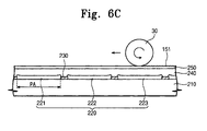
- FIGS. 6A to 6C are sectional views illustrating a method of forming the color filter substrate shown in FIG. 5 .
- the color filter 220 and the black matrix 230 are formed on the second base substrate 210 , and then the overcoat layer 240 is formed on the color filter 220 and the black matrix 230 .
- a second alignment layer 260 including the polyimide is coated over the overcoat layer 240 .
- the second alignment layer 260 may be formed by the inkjet method applied when the first alignment layer 150 is formed as shown in FIG. 3B , or may be formed by a rolling method using a roller.
- the krypton fluoride laser 20 is irradiated onto the second alignment layer 260 to allow the second alignment layer 260 to have the electrical conductivity, so that the common electrode 250 is formed.
- the second alignment pattern 251 is formed on the upper face of the common electrode 251 .
- the common electrode 250 includes the polyimide material having the electrical conductivity generated by irradiating the krypton fluoride laser 20 onto the polyimide material, so that the common electrode 250 may be provided with the second alignment pattern 251 formed thereon by using a rubbing method.
- the manufacturing cost of the color filter substrate 200 may be reduced, and the productivity of the color filter substrate 200 may be enhanced.
- FIG. 7 is a cross-sectional view showing an exemplary embodiment of a liquid crystal display according to the present invention.
- a liquid crystal display panel 400 includes the array substrate 100 , the color filter substrate 200 facing the array substrate 100 , and a liquid crystal layer 300 disposed between the array substrate 100 and the color filter substrate 200 .
- the array substrate 100 has same structure and function as those of the array substrate shown in FIGS. 1 and 2
- the color filter substrate 200 has also same structure and function as those of the color filter substrate shown in FIGS. 4 and 5 .
- detailed descriptions of the array substrate 100 and the color filter substrate 200 will be omitted in order to avoid redundancy.
- the array substrate 100 includes the first base substrate 110 , the gate line GL (refer to FIG. 1 ), the data line DL (refer to FIG. 1 ), the thin film transistor 120 and the pixel electrode 130 .
- the pixel electrode 130 includes the conductive polyimide and is provided with the first alignment pattern 131 formed thereon to align the liquid crystal molecules 310 of the liquid crystal layer 300 .
- the array substrate 100 may further include insulation layers as the gate insulation layer 141 , the protection layer 142 , and the organic insulation layer 143 .
- the color filter substrate 200 is positioned at an upper portion of the array substrate 100 such that the color filter substrate 200 faces the array substrate 100 .
- the color filter substrate 200 includes the second base substrate 210 , the color filter 220 , the black matrix 230 , the overcoat layer 240 , and the common electrode 250 .
- the common electrode 250 includes the conductive polyimide material and is provided with the second alignment pattern 251 formed thereon to align the liquid crystal molecules 310 of the liquid crystal layer 300 .
- the second alignment pattern 251 is formed in a direction substantially perpendicular to the first alignment pattern 131 .
- the pixel electrode 130 and the common electrode 250 include the conductive polyimide material and are provided with the first and second alignment patterns 131 and 251 formed thereon, respectively.
- the array substrate 100 and the color filter substrate 200 do not need to have separate alignment layer, thereby reducing the manufacturing cost and the process complexity for the liquid crystal display panel 400 and enhancing the productivity of the liquid crystal display panel 400 .
- the liquid crystal layer 300 controls the transmittance of the light passing therethrough in accordance with the electric field formed between the pixel electrode 130 and the common electrode 250 .
- the light exiting through the liquid crystal layer 300 is provided to the color filter 220 , so that the image may be displayed on the liquid crystal display panel 400 .
- FIG. 8 is a flowchart illustrating a method of manufacturing the liquid crystal display panel according to the present invention.
- the gate line GL, the data line DL, the thin film transistor 120 , the pixel electrode 130 , the gate insulation layer 141 , the protection layer 142 and the organic insulation layer 143 are formed on the first base substrate 110 , so that the array substrate 100 is completed (S 110 ).
- the process of manufacturing the array substrate 100 is identical with the process of manufacturing the array substrate shown in FIGS. 3A to 3D , and thus detailed description of the process for the array substrate 100 will be omitted.
- the color filter 220 , the black matrix 230 , the overcoat layer 240 and the common electrode 250 are formed on the second base substrate 210 , so that the color filter substrate 200 is completed (S 120 ).
- the process of manufacturing the color filter substrate 200 is identical with the process of manufacturing the color filter substrate shown in FIGS. 6A to 6C , and thus detailed description of the process for the color filter substrate 100 will be omitted.
- the liquid crystal molecules 310 are dropped onto any of the array substrate 100 and the color filter substrate 200 to form the liquid crystal layer 300 (S 130 )
- the array substrate 100 is coupled with the color filter substrate 200 while disposing the liquid crystal layer 300 between the array substrate 100 and the color filter substrate 200 , so that the liquid crystal display panel 400 is completed (S 140 ).
- the array substrate 100 and the color filter substrate 200 are coupled with each other after the liquid crystal layer 300 is formed on the array substrate 100 or the color filter substrate 200 .
- the liquid crystal layer 300 may be formed by a vacuum injection method after coupling the array substrate 100 with the color filter substrate 200 .
- the pixel electrode and the common electrode include the conductive polyimide material and are provided with the alignment pattern formed thereon, respectively.
- the liquid crystal display panel does not need to have the separate alignment layer, so that the manufacturing cost and the process complexity may be reduced and the productivity may be enhanced.
Abstract
Description
Claims (7)
Applications Claiming Priority (3)
| Application Number | Priority Date | Filing Date | Title |
|---|---|---|---|
| KR10-2006-0135303 | 2006-12-27 | ||
| KR10-2006-00135303 | 2006-12-27 | ||
| KR1020060135303A KR101355145B1 (en) | 2006-12-27 | 2006-12-27 | Array substrate and colorfilter substrate, liquid crystal display having the same and method of fabricating the same |
Publications (2)
| Publication Number | Publication Date |
|---|---|
| US20080158459A1 US20080158459A1 (en) | 2008-07-03 |
| US8040477B2 true US8040477B2 (en) | 2011-10-18 |
Family
ID=39583373
Family Applications (1)
| Application Number | Title | Priority Date | Filing Date |
|---|---|---|---|
| US11/958,193 Active 2028-07-25 US8040477B2 (en) | 2006-12-27 | 2007-12-17 | Array substrate, liquid crystal display panel, and method of manufacturing the same |
Country Status (2)
| Country | Link |
|---|---|
| US (1) | US8040477B2 (en) |
| KR (1) | KR101355145B1 (en) |
Cited By (1)
| Publication number | Priority date | Publication date | Assignee | Title |
|---|---|---|---|---|
| US11646319B2 (en) | 2019-12-12 | 2023-05-09 | Lg Display Co., Ltd. | Polyimide substrate including intaglio patterns and display device including the same |
Families Citing this family (3)
| Publication number | Priority date | Publication date | Assignee | Title |
|---|---|---|---|---|
| KR100579192B1 (en) * | 2004-03-11 | 2006-05-11 | 삼성에스디아이 주식회사 | Top-emission type organic electro luminescence display device and method for fabricating of the same |
| KR101359297B1 (en) * | 2012-05-18 | 2014-02-11 | 박경진 | Device for controlling light-amount without an alignment layer and system including the same |
| CN106773397B (en) * | 2016-12-26 | 2023-09-15 | 合肥京东方光电科技有限公司 | Array substrate, preparation method thereof and liquid crystal display device |
Citations (8)
| Publication number | Priority date | Publication date | Assignee | Title |
|---|---|---|---|---|
| KR100203304B1 (en) | 1996-05-22 | 1999-06-15 | 김영환 | A menufacture method of active matrix liquid crystal display device |
| US5949509A (en) * | 1997-05-22 | 1999-09-07 | Hitachi, Ltd. | Active matrix liquid crystal display device method for checking the alignment ability of a photo-alignment layer |
| JP2001021891A (en) | 1999-07-02 | 2001-01-26 | Toshiba Corp | Manufacture of liquid crystal display and liquid crystal display |
| US20020057408A1 (en) * | 1997-01-24 | 2002-05-16 | Kazuhiro Nishiyama | Homeotropic and hybrid alignment types of liquid crystal displays and a manufacturing method thereof |
| JP2004053784A (en) | 2002-07-18 | 2004-02-19 | Sharp Corp | Liquid crystal display device and method for manufacturing the same |
| US20040091641A1 (en) * | 2001-05-24 | 2004-05-13 | Lg. Phillips Lcd Co., Ltd. | Liquid crystal display device and fabricating method thereof, and reworking method of alignment film using the same |
| US7118787B2 (en) * | 2001-06-29 | 2006-10-10 | University Of Hull | Liquid crystal alignment layer |
| US20070154659A1 (en) * | 2005-12-29 | 2007-07-05 | Lg.Philips Lcd Co., Ltd. | Rubbing membrane material and liquid crystal display device using the same |
Family Cites Families (3)
| Publication number | Priority date | Publication date | Assignee | Title |
|---|---|---|---|---|
| KR100840669B1 (en) * | 2001-08-21 | 2008-06-24 | 엘지디스플레이 주식회사 | A Method For Fabricating Liquid Crystal Display Device By Using Thermal Crosslinking Polyimide Based Material |
| CN100430802C (en) * | 2002-12-09 | 2008-11-05 | 株式会社日立显示器 | Liquid crystal display and method for manufacturing same |
| KR100551229B1 (en) * | 2003-06-26 | 2006-02-10 | 주식회사 디피아이 솔루션스 | Method of making organic transparent electrode for display |
-
2006
- 2006-12-27 KR KR1020060135303A patent/KR101355145B1/en active IP Right Grant
-
2007
- 2007-12-17 US US11/958,193 patent/US8040477B2/en active Active
Patent Citations (8)
| Publication number | Priority date | Publication date | Assignee | Title |
|---|---|---|---|---|
| KR100203304B1 (en) | 1996-05-22 | 1999-06-15 | 김영환 | A menufacture method of active matrix liquid crystal display device |
| US20020057408A1 (en) * | 1997-01-24 | 2002-05-16 | Kazuhiro Nishiyama | Homeotropic and hybrid alignment types of liquid crystal displays and a manufacturing method thereof |
| US5949509A (en) * | 1997-05-22 | 1999-09-07 | Hitachi, Ltd. | Active matrix liquid crystal display device method for checking the alignment ability of a photo-alignment layer |
| JP2001021891A (en) | 1999-07-02 | 2001-01-26 | Toshiba Corp | Manufacture of liquid crystal display and liquid crystal display |
| US20040091641A1 (en) * | 2001-05-24 | 2004-05-13 | Lg. Phillips Lcd Co., Ltd. | Liquid crystal display device and fabricating method thereof, and reworking method of alignment film using the same |
| US7118787B2 (en) * | 2001-06-29 | 2006-10-10 | University Of Hull | Liquid crystal alignment layer |
| JP2004053784A (en) | 2002-07-18 | 2004-02-19 | Sharp Corp | Liquid crystal display device and method for manufacturing the same |
| US20070154659A1 (en) * | 2005-12-29 | 2007-07-05 | Lg.Philips Lcd Co., Ltd. | Rubbing membrane material and liquid crystal display device using the same |
Cited By (1)
| Publication number | Priority date | Publication date | Assignee | Title |
|---|---|---|---|---|
| US11646319B2 (en) | 2019-12-12 | 2023-05-09 | Lg Display Co., Ltd. | Polyimide substrate including intaglio patterns and display device including the same |
Also Published As
| Publication number | Publication date |
|---|---|
| US20080158459A1 (en) | 2008-07-03 |
| KR20080060794A (en) | 2008-07-02 |
| KR101355145B1 (en) | 2014-02-04 |
Similar Documents
| Publication | Publication Date | Title |
|---|---|---|
| US7405798B2 (en) | Liquid crystal display apparatus and method of forming the same | |
| US7817227B2 (en) | Array substrate, display panel having the same and method of manufacturing the same | |
| US6567150B1 (en) | Liquid crystal display and method of manufacturing the same | |
| KR100442510B1 (en) | Active matrix substrate and production method thereof, liquid crystal display, flat panel display and image sensing device and production method thereof | |
| JP3332773B2 (en) | Active matrix substrate and method of manufacturing active matrix substrate | |
| KR101620526B1 (en) | Method of making liquid crystal display and liquid crystal display thereof | |
| US9046714B2 (en) | Thin film transistor substrate and method for fabricating the same | |
| US7671956B2 (en) | Liquid crystal display panel and fabricating method thereof | |
| US8040477B2 (en) | Array substrate, liquid crystal display panel, and method of manufacturing the same | |
| KR100763169B1 (en) | Structure of vacuum chuck for adsorbing substrate | |
| US8012845B2 (en) | Insulating film pattern, method for manufacturing the same, and method for manufacturing thin film transistor substrate using the same | |
| US7696027B2 (en) | Method of fabricating display substrate and method of fabricating display panel using the same | |
| US6157431A (en) | Liquid crystal display apparatus suppressed of orientation defect having metal film and photosensitive resin as a columnar spacer and fabrication method thereof | |
| US20080149933A1 (en) | Display panel | |
| KR20020027727A (en) | liquid crystal display and manufacturing method thereof | |
| US8530291B2 (en) | Method for manufacturing display device | |
| JP2009271105A (en) | Method for manufacturing liquid crystal display device | |
| KR100268105B1 (en) | Thin-film transistor substrate and manufacturing method thereof | |
| KR100962499B1 (en) | Liquid crystal display panel and fabrication apparatus and method thereof | |
| CN113140575B (en) | Array substrate, preparation method thereof, display panel and display device | |
| JPH10305369A (en) | Liquid crystal display and manufacture | |
| JP2008032855A (en) | Liquid crystal display | |
| KR101396720B1 (en) | liquid crystal display device and method for fabricating the same | |
| KR20080038593A (en) | Liquid crystal display panel and fabricating method thereof | |
| KR20090035976A (en) | Liquid crystal display device and method of manufacturing the same |
Legal Events
| Date | Code | Title | Description |
|---|---|---|---|
| AS | Assignment |
Owner name: SAMSUNG ELECTRONICS CO., LTD., KOREA, REPUBLIC OF Free format text: ASSIGNMENT OF ASSIGNORS INTEREST;ASSIGNORS:LEE, JUN-HYUP;YOON, YEO-GEON;REEL/FRAME:020262/0207 Effective date: 20071129 |
|
| FEPP | Fee payment procedure |
Free format text: PAYOR NUMBER ASSIGNED (ORIGINAL EVENT CODE: ASPN); ENTITY STATUS OF PATENT OWNER: LARGE ENTITY |
|
| STCF | Information on status: patent grant |
Free format text: PATENTED CASE |
|
| AS | Assignment |
Owner name: SAMSUNG DISPLAY CO., LTD., KOREA, REPUBLIC OF Free format text: ASSIGNMENT OF ASSIGNORS INTEREST;ASSIGNOR:SAMSUNG ELECTRONICS CO., LTD.;REEL/FRAME:029008/0028 Effective date: 20120904 |
|
| FPAY | Fee payment |
Year of fee payment: 4 |
|
| MAFP | Maintenance fee payment |
Free format text: PAYMENT OF MAINTENANCE FEE, 8TH YEAR, LARGE ENTITY (ORIGINAL EVENT CODE: M1552); ENTITY STATUS OF PATENT OWNER: LARGE ENTITY Year of fee payment: 8 |
|
| MAFP | Maintenance fee payment |
Free format text: PAYMENT OF MAINTENANCE FEE, 12TH YEAR, LARGE ENTITY (ORIGINAL EVENT CODE: M1553); ENTITY STATUS OF PATENT OWNER: LARGE ENTITY Year of fee payment: 12 |