US11646319B2 - Polyimide substrate including intaglio patterns and display device including the same - Google Patents
Polyimide substrate including intaglio patterns and display device including the same Download PDFInfo
- Publication number
- US11646319B2 US11646319B2 US17/109,941 US202017109941A US11646319B2 US 11646319 B2 US11646319 B2 US 11646319B2 US 202017109941 A US202017109941 A US 202017109941A US 11646319 B2 US11646319 B2 US 11646319B2
- Authority
- US
- United States
- Prior art keywords
- polyimide substrate
- disposed
- display device
- transmittance
- filling
- Prior art date
- Legal status (The legal status is an assumption and is not a legal conclusion. Google has not performed a legal analysis and makes no representation as to the accuracy of the status listed.)
- Active, expires
Links
- 239000000758 substrate Substances 0.000 title claims abstract description 196
- 239000004642 Polyimide Substances 0.000 title claims abstract description 186
- 229920001721 polyimide Polymers 0.000 title claims abstract description 186
- 238000002834 transmittance Methods 0.000 claims abstract description 92
- 230000005540 biological transmission Effects 0.000 claims description 38
- 239000010409 thin film Substances 0.000 claims description 23
- 239000000463 material Substances 0.000 claims description 18
- 238000009413 insulation Methods 0.000 claims description 14
- 229910021420 polycrystalline silicon Inorganic materials 0.000 claims description 2
- 238000000034 method Methods 0.000 abstract description 34
- 230000001965 increasing effect Effects 0.000 description 17
- 239000010408 film Substances 0.000 description 5
- VYPSYNLAJGMNEJ-UHFFFAOYSA-N Silicium dioxide Chemical compound O=[Si]=O VYPSYNLAJGMNEJ-UHFFFAOYSA-N 0.000 description 4
- 238000005070 sampling Methods 0.000 description 4
- 229910004205 SiNX Inorganic materials 0.000 description 2
- XLOMVQKBTHCTTD-UHFFFAOYSA-N Zinc monoxide Chemical compound [Zn]=O XLOMVQKBTHCTTD-UHFFFAOYSA-N 0.000 description 2
- 230000009286 beneficial effect Effects 0.000 description 2
- 229910052681 coesite Inorganic materials 0.000 description 2
- 229910052906 cristobalite Inorganic materials 0.000 description 2
- 230000002708 enhancing effect Effects 0.000 description 2
- 238000005530 etching Methods 0.000 description 2
- 239000011521 glass Substances 0.000 description 2
- 239000004973 liquid crystal related substance Substances 0.000 description 2
- 239000000377 silicon dioxide Substances 0.000 description 2
- 229910052682 stishovite Inorganic materials 0.000 description 2
- 229910052905 tridymite Inorganic materials 0.000 description 2
- -1 Siloxan Chemical class 0.000 description 1
- 238000007792 addition Methods 0.000 description 1
- 229910052810 boron oxide Inorganic materials 0.000 description 1
- 239000011248 coating agent Substances 0.000 description 1
- 238000000576 coating method Methods 0.000 description 1
- JKWMSGQKBLHBQQ-UHFFFAOYSA-N diboron trioxide Chemical compound O=BOB=O JKWMSGQKBLHBQQ-UHFFFAOYSA-N 0.000 description 1
- 239000007772 electrode material Substances 0.000 description 1
- 229910003437 indium oxide Inorganic materials 0.000 description 1
- PJXISJQVUVHSOJ-UHFFFAOYSA-N indium(iii) oxide Chemical compound [O-2].[O-2].[O-2].[In+3].[In+3] PJXISJQVUVHSOJ-UHFFFAOYSA-N 0.000 description 1
- 238000004519 manufacturing process Methods 0.000 description 1
- 238000012986 modification Methods 0.000 description 1
- 230000004048 modification Effects 0.000 description 1
- UJMWVICAENGCRF-UHFFFAOYSA-N oxygen difluoride Chemical compound FOF UJMWVICAENGCRF-UHFFFAOYSA-N 0.000 description 1
- 238000005498 polishing Methods 0.000 description 1
- 239000000126 substance Substances 0.000 description 1
- 238000006467 substitution reaction Methods 0.000 description 1
- 239000011787 zinc oxide Substances 0.000 description 1
Images


Classifications
-
- H—ELECTRICITY
- H01—ELECTRIC ELEMENTS
- H01L—SEMICONDUCTOR DEVICES NOT COVERED BY CLASS H10
- H01L27/00—Devices consisting of a plurality of semiconductor or other solid-state components formed in or on a common substrate
- H01L27/02—Devices consisting of a plurality of semiconductor or other solid-state components formed in or on a common substrate including semiconductor components specially adapted for rectifying, oscillating, amplifying or switching and having at least one potential-jump barrier or surface barrier; including integrated passive circuit elements with at least one potential-jump barrier or surface barrier
- H01L27/12—Devices consisting of a plurality of semiconductor or other solid-state components formed in or on a common substrate including semiconductor components specially adapted for rectifying, oscillating, amplifying or switching and having at least one potential-jump barrier or surface barrier; including integrated passive circuit elements with at least one potential-jump barrier or surface barrier the substrate being other than a semiconductor body, e.g. an insulating body
- H01L27/1214—Devices consisting of a plurality of semiconductor or other solid-state components formed in or on a common substrate including semiconductor components specially adapted for rectifying, oscillating, amplifying or switching and having at least one potential-jump barrier or surface barrier; including integrated passive circuit elements with at least one potential-jump barrier or surface barrier the substrate being other than a semiconductor body, e.g. an insulating body comprising a plurality of TFTs formed on a non-semiconducting substrate, e.g. driving circuits for AMLCDs
- H01L27/1218—Devices consisting of a plurality of semiconductor or other solid-state components formed in or on a common substrate including semiconductor components specially adapted for rectifying, oscillating, amplifying or switching and having at least one potential-jump barrier or surface barrier; including integrated passive circuit elements with at least one potential-jump barrier or surface barrier the substrate being other than a semiconductor body, e.g. an insulating body comprising a plurality of TFTs formed on a non-semiconducting substrate, e.g. driving circuits for AMLCDs with a particular composition or structure of the substrate
-
- H—ELECTRICITY
- H01—ELECTRIC ELEMENTS
- H01L—SEMICONDUCTOR DEVICES NOT COVERED BY CLASS H10
- H01L25/00—Assemblies consisting of a plurality of individual semiconductor or other solid state devices ; Multistep manufacturing processes thereof
- H01L25/03—Assemblies consisting of a plurality of individual semiconductor or other solid state devices ; Multistep manufacturing processes thereof all the devices being of a type provided for in the same subgroup of groups H01L27/00 - H01L33/00, or in a single subclass of H10K, H10N, e.g. assemblies of rectifier diodes
- H01L25/04—Assemblies consisting of a plurality of individual semiconductor or other solid state devices ; Multistep manufacturing processes thereof all the devices being of a type provided for in the same subgroup of groups H01L27/00 - H01L33/00, or in a single subclass of H10K, H10N, e.g. assemblies of rectifier diodes the devices not having separate containers
- H01L25/075—Assemblies consisting of a plurality of individual semiconductor or other solid state devices ; Multistep manufacturing processes thereof all the devices being of a type provided for in the same subgroup of groups H01L27/00 - H01L33/00, or in a single subclass of H10K, H10N, e.g. assemblies of rectifier diodes the devices not having separate containers the devices being of a type provided for in group H01L33/00
- H01L25/0753—Assemblies consisting of a plurality of individual semiconductor or other solid state devices ; Multistep manufacturing processes thereof all the devices being of a type provided for in the same subgroup of groups H01L27/00 - H01L33/00, or in a single subclass of H10K, H10N, e.g. assemblies of rectifier diodes the devices not having separate containers the devices being of a type provided for in group H01L33/00 the devices being arranged next to each other
-
- H—ELECTRICITY
- H01—ELECTRIC ELEMENTS
- H01L—SEMICONDUCTOR DEVICES NOT COVERED BY CLASS H10
- H01L25/00—Assemblies consisting of a plurality of individual semiconductor or other solid state devices ; Multistep manufacturing processes thereof
- H01L25/16—Assemblies consisting of a plurality of individual semiconductor or other solid state devices ; Multistep manufacturing processes thereof the devices being of types provided for in two or more different main groups of groups H01L27/00 - H01L33/00, or in a single subclass of H10K, H10N, e.g. forming hybrid circuits
- H01L25/167—Assemblies consisting of a plurality of individual semiconductor or other solid state devices ; Multistep manufacturing processes thereof the devices being of types provided for in two or more different main groups of groups H01L27/00 - H01L33/00, or in a single subclass of H10K, H10N, e.g. forming hybrid circuits comprising optoelectronic devices, e.g. LED, photodiodes
-
- H—ELECTRICITY
- H10—SEMICONDUCTOR DEVICES; ELECTRIC SOLID-STATE DEVICES NOT OTHERWISE PROVIDED FOR
- H10K—ORGANIC ELECTRIC SOLID-STATE DEVICES
- H10K77/00—Constructional details of devices covered by this subclass and not covered by groups H10K10/80, H10K30/80, H10K50/80 or H10K59/80
- H10K77/10—Substrates, e.g. flexible substrates
-
- B—PERFORMING OPERATIONS; TRANSPORTING
- B32—LAYERED PRODUCTS
- B32B—LAYERED PRODUCTS, i.e. PRODUCTS BUILT-UP OF STRATA OF FLAT OR NON-FLAT, e.g. CELLULAR OR HONEYCOMB, FORM
- B32B2379/00—Other polymers having nitrogen, with or without oxygen or carbon only, in the main chain
- B32B2379/08—Polyimides
-
- G—PHYSICS
- G09—EDUCATION; CRYPTOGRAPHY; DISPLAY; ADVERTISING; SEALS
- G09G—ARRANGEMENTS OR CIRCUITS FOR CONTROL OF INDICATING DEVICES USING STATIC MEANS TO PRESENT VARIABLE INFORMATION
- G09G2300/00—Aspects of the constitution of display devices
- G09G2300/04—Structural and physical details of display devices
- G09G2300/0404—Matrix technologies
- G09G2300/0408—Integration of the drivers onto the display substrate
-
- G—PHYSICS
- G09—EDUCATION; CRYPTOGRAPHY; DISPLAY; ADVERTISING; SEALS
- G09G—ARRANGEMENTS OR CIRCUITS FOR CONTROL OF INDICATING DEVICES USING STATIC MEANS TO PRESENT VARIABLE INFORMATION
- G09G2300/00—Aspects of the constitution of display devices
- G09G2300/08—Active matrix structure, i.e. with use of active elements, inclusive of non-linear two terminal elements, in the pixels together with light emitting or modulating elements
- G09G2300/0804—Sub-multiplexed active matrix panel, i.e. wherein one active driving circuit is used at pixel level for multiple image producing elements
-
- H—ELECTRICITY
- H01—ELECTRIC ELEMENTS
- H01L—SEMICONDUCTOR DEVICES NOT COVERED BY CLASS H10
- H01L27/00—Devices consisting of a plurality of semiconductor or other solid-state components formed in or on a common substrate
- H01L27/15—Devices consisting of a plurality of semiconductor or other solid-state components formed in or on a common substrate including semiconductor components with at least one potential-jump barrier or surface barrier specially adapted for light emission
- H01L27/153—Devices consisting of a plurality of semiconductor or other solid-state components formed in or on a common substrate including semiconductor components with at least one potential-jump barrier or surface barrier specially adapted for light emission in a repetitive configuration, e.g. LED bars
- H01L27/156—Devices consisting of a plurality of semiconductor or other solid-state components formed in or on a common substrate including semiconductor components with at least one potential-jump barrier or surface barrier specially adapted for light emission in a repetitive configuration, e.g. LED bars two-dimensional arrays
-
- H01L27/3244—
-
- H01L51/0097—
-
- H—ELECTRICITY
- H10—SEMICONDUCTOR DEVICES; ELECTRIC SOLID-STATE DEVICES NOT OTHERWISE PROVIDED FOR
- H10K—ORGANIC ELECTRIC SOLID-STATE DEVICES
- H10K2102/00—Constructional details relating to the organic devices covered by this subclass
- H10K2102/301—Details of OLEDs
- H10K2102/351—Thickness
-
- H—ELECTRICITY
- H10—SEMICONDUCTOR DEVICES; ELECTRIC SOLID-STATE DEVICES NOT OTHERWISE PROVIDED FOR
- H10K—ORGANIC ELECTRIC SOLID-STATE DEVICES
- H10K59/00—Integrated devices, or assemblies of multiple devices, comprising at least one organic light-emitting element covered by group H10K50/00
- H10K59/10—OLED displays
- H10K59/12—Active-matrix OLED [AMOLED] displays
- H10K59/121—Active-matrix OLED [AMOLED] displays characterised by the geometry or disposition of pixel elements
-
- H—ELECTRICITY
- H10—SEMICONDUCTOR DEVICES; ELECTRIC SOLID-STATE DEVICES NOT OTHERWISE PROVIDED FOR
- H10K—ORGANIC ELECTRIC SOLID-STATE DEVICES
- H10K77/00—Constructional details of devices covered by this subclass and not covered by groups H10K10/80, H10K30/80, H10K50/80 or H10K59/80
- H10K77/10—Substrates, e.g. flexible substrates
- H10K77/111—Flexible substrates
-
- Y—GENERAL TAGGING OF NEW TECHNOLOGICAL DEVELOPMENTS; GENERAL TAGGING OF CROSS-SECTIONAL TECHNOLOGIES SPANNING OVER SEVERAL SECTIONS OF THE IPC; TECHNICAL SUBJECTS COVERED BY FORMER USPC CROSS-REFERENCE ART COLLECTIONS [XRACs] AND DIGESTS
- Y02—TECHNOLOGIES OR APPLICATIONS FOR MITIGATION OR ADAPTATION AGAINST CLIMATE CHANGE
- Y02E—REDUCTION OF GREENHOUSE GAS [GHG] EMISSIONS, RELATED TO ENERGY GENERATION, TRANSMISSION OR DISTRIBUTION
- Y02E10/00—Energy generation through renewable energy sources
- Y02E10/50—Photovoltaic [PV] energy
- Y02E10/549—Organic PV cells
Definitions
- Embodiments of the disclosure are related to polyimide substrates and display devices.
- a display device may be implemented in various types, for example, the display device may be implemented as a transparent display device which has a high transmittance and appears transparent while not displaying an image.
- the inventors of the present disclosure have realized that when a substrate having a high transmittance is used, it is possible to affect a process of a display device due to a decrease in other characteristics (e.g., heat resistance, etc.). Accordingly, there are many technical difficulties in implementing a transparent display device. However, the inventors were able to provide a method to implement a transparent display device having a high transmittance by increasing a transmittance of a polyimide substrate included in a display device while maintaining a heat resistance of the polyimide substrate.
- Embodiments of the disclosure provide a method to maintain a heat resistance of a polyimide substrate and increase a transmittance of the polyimide substrate in a process of a display device.
- a display device comprises a polyimide substrate having a first transmittance, comprising a plurality of intaglio patterns located on at least a portion of one surface, and wherein a filling is disposed in the plurality of intaglio patterns and the filling has a second transmittance greater than the first transmittance, and a plurality of subpixels disposed on the polyimide substrate, comprising a light emission portion where a light emitting element is disposed, a circuit portion where a thin film transistor is disposed, and a transmission portion located on at least a portion of an area except for an area where the light emission portion and the circuit portion are disposed.
- a display device comprises a polyimide substrate, and a plurality of subpixels disposed on the polyimide substrate, comprising a light emission portion where a light emitting element is disposed, a circuit portion where a thin film transistor is disposed, and a transmission portion located on at least a portion of an area except for an area where the light emission portion and the circuit portion are disposed, wherein a top surface of the polyimide substrate comprises a plurality of intaglio patterns located on at least a portion of an area overlapped with the transmission portion.
- a polyimide substrate comprises a first portion having a first thickness and a first transmittance, and a plurality of second portion connected to the first portion, a portion corresponding to a second thickness smaller than the first thickness has the first transmittance, and the other portion corresponding to a third thickness excluding the second thickness from the first thickness has a second transmittance greater than the first transmittance.
- an intaglio pattern is formed in one surface of a polyimide substrate, a filling having a higher transmittance than a colored polyimide and a lower coefficient of thermal expansion than a transparent polyimide is disposed in the intaglio pattern, thus a transmittance of the polyimide substrate could be enhanced while maintaining a heat resistance of the polyimide substrate.
- a filling is disposed in an intaglio pattern of a polyimide substrate and a planarization process is performed, thus the polyimide substrate having high transmittance and heat resistance could be implemented in a process of a display device.
- FIG. 1 is a view schematically illustrating a configuration of a display device according to various embodiments of the disclosure
- FIG. 2 is a view illustrating an example of a structure which a display device according to various embodiments of the disclosure is implemented as a transparent display device;
- FIG. 3 is a view illustrating an example of a structure of a polyimide substrate according to various embodiments of the disclosure
- FIG. 4 is a view illustrating an example of a process scheme of a polyimide substrate according to various embodiments of the disclosure
- FIG. 5 is a view illustrating other example of a structure of a polyimide substrate according to various embodiments of the disclosure.
- FIGS. 6 A, 6 B, and 6 C are views illustrating an example of a shape of an intaglio pattern included in a polyimide substrate according to various embodiments of the disclosure.
- FIGS. 7 and 8 are views illustrating examples of areas where an intaglio pattern is disposed in a polyimide substrate according types of a display device.
- first element is connected or coupled to,” “contacts or overlaps,” etc., a second element
- first element is connected or coupled to
- contacts or overlaps etc.
- second element it should be interpreted that, not only can the first element “be directly connected or coupled to” or “directly contact or overlap” the second element, but a third element can also be “interposed” between the first and second elements, or the first and second elements can “be connected or coupled to,” “contact or overlap,” etc., each other via a fourth element.
- the second element may be included in at least one of two or more elements that “are connected or coupled to,” “contact or overlap,” etc., each other.
- time relative terms such as “after,” “subsequent to,” “next,” “before,” and the like, are used to describe processes or operations of elements or configurations, or flows or steps in operating, processing, manufacturing methods, these terms may be used to describe non-consecutive or non-sequential processes or operations unless the term “directly” or “immediately” is used together.
- FIG. 1 is a view schematically illustrating a configuration of a display device 100 according to various embodiments of the disclosure.
- a display device 100 may include a display panel 110 including an active area AA and a non-active area NA, a gate driving circuit 120 , a data driving circuit 130 , and a controller 140 for driving the display panel 110 .
- the display panel 110 may include a plurality of gate lines GL, a plurality of data lines DL, and subpixels SP adjacent at the overlapping locations of the gate lines GL and the data lines DL.
- the gate driving circuit 120 may be controlled by the controller 140 to sequentially output scan signals to the plurality of gate lines GL disposed in the display panel 110 , controlling the driving timing of the subpixels SP.
- the gate driving circuit 120 may include one or more gate driver integrated circuits (GDICs). Depending on driving schemes, the gate driving circuit 120 may be positioned on only one side, or each of two opposite sides, of the display panel 110 .
- GDICs gate driver integrated circuits
- Each gate driver integrated circuit may be connected to a bonding pad of the display panel 110 by a tape automated bonding (TAB) scheme or a chip on glass (COG) scheme, or may be directly disposed on the display panel 110 by implementing as a GIP (Gate In Panel) type, in some cases, may be integrated and disposed on the display panel 110 .
- each gate driver integrated circuit may be implemented by a chip on film (COF) scheme which each gate driver integrated circuit (GDIC) is mounted on a film connected to the display panel 110 .
- COF chip on film
- the data driving circuit 130 receives image data from the controller 140 and converts the image data into an analog data voltage.
- the data driving circuit 130 outputs a data voltage to each data line DL according to the timing of applying a scan signal via the gate line GL, allowing each subpixel SP to represent a brightness according to the image data.
- the data driving circuit 130 may include one or more source driver integrated circuits (SDICs).
- SDICs source driver integrated circuits
- Each source driver integrated circuit may include a shift register, a latch circuit, a digital to analog converter, an output buffer, and the like.
- Each source driver integrated circuit may be connected to a bonding pad of the display panel 110 by a tape automated bonding (TAB) scheme or a chip on glass (COG) scheme, or may be directly disposed on the display panel 110 , in some cases, may be integrated and disposed on the display panel 110 .
- each source driver integrated circuit may be implemented by a chip on film (COF) scheme, in this case, each source driver integrated circuit (SDIC) may be mounted on a film connected to the display panel 110 and electrically connected to the display panel 110 through wires on the film.
- the controller 140 supplies various control signals to the gate driving circuit 120 and the data driving circuit 130 and controls the operation of the gate driving circuit 120 and the data driving circuit 130 .
- the controller 140 is mounted on a printed circuit board, a flexible printed circuit, and the like, and electrically connected to the gate driving circuit 120 and the data driving circuit 130 through the printed circuit board, the flexible printed circuit, and the like.
- the controller 140 enables the gate driving circuit 120 to output scan signals according to the timing of implementing each frame, converts image data received from the outside to meet the data signal format used by the data driving circuit 130 , and outputs the resultant image data to the data driving circuit 130 .
- the controller 140 receives, from the outside (e.g., a host system), various timing signals including a vertical synchronization signal VSYNC, a horizontal synchronization signal HSYNC, an input data enable signal DE, and a clock signal, along with the image data.
- various timing signals including a vertical synchronization signal VSYNC, a horizontal synchronization signal HSYNC, an input data enable signal DE, and a clock signal, along with the image data.
- the controller 140 may generate a diversity of control signals using the timing signals received from the outside and output the control signals to the gate driving circuit 120 and the data driving circuit 130 .
- the controller 140 outputs various gate control signals GCS including a gate start pulse GSP, a gate shift clock GSC, and a gate output enable signal GOE.
- the gate start pulse GSP controls the operation start timing of one or more gate driver integrated circuits (GDICs) constituting the gate driving circuit 120 .
- the gate shift clock GSC is a clock signal commonly input to one or more gate driver integrated circuits (GDICs) and controls the shift timing of the scan signals.
- the gate output enable signal GOE designates timing information about one or more gate driver integrated circuits (GDICs).
- the controller 140 To control the data driving circuit 130 , the controller 140 outputs various data control signals DCS including, e.g., a source start pulse SSP, a source sampling clock SSC, and a source output enable signal SOE.
- DCS data control signals including, e.g., a source start pulse SSP, a source sampling clock SSC, and a source output enable signal SOE.
- the source start pulse SSP controls the data sampling start timing of one or more source driver integrated circuits (SDICs) constituting the data driving circuit 130 .
- the source sampling clock SSC is a clock signal for controlling the sampling timing of data in each source driver integrated circuit (SDIC).
- the source output enable signal SOE controls the output timing of the data driving circuit 130 .
- the display device 100 may further include a power management integrated circuit that supplies various voltages or currents to, e.g., the display panel 110 , the gate driving circuit 120 , and the data driving circuit 130 or controls various voltages or currents to be supplied.
- a power management integrated circuit that supplies various voltages or currents to, e.g., the display panel 110 , the gate driving circuit 120 , and the data driving circuit 130 or controls various voltages or currents to be supplied.
- Each of subpixels SPs is at an area adjacently formed at the crossings of the gate line GL and the data line DL.
- a liquid crystal or a light emitting element may be disposed in the subpixel SP.
- the light emitting element for example, may be an organic light emitting diode (OLED) or an inorganic light emitting diode (LED), in some cases, may be a micro light emitting diode ( ⁇ LED) having a size of dozens of micrometers ( ⁇ m).
- the subpixel SP may include a transparent area where a circuit element and the like is not disposed in an area except for an area where the circuit element or the light emitting element are not disposed. That is, when the display device 100 is a transparent display device, the subpixel SP may include the transparent area.
- FIG. 2 is a view illustrating an example of a structure which a display device 100 according to various embodiments of the disclosure is implemented as a transparent display device.
- a thin film transistor layer 220 on where a plurality of thin film transistors for driving a light emitting element are disposed may be positioned on a lower substrate 210 .
- An area where the thin film transistor is disposed may be regarded as a circuit portion CA on a plane.
- a light emitting element layer 230 on where a plurality of light emitting elements are disposed may be positioned on the thin film transistor layer 220 .
- An area where the light emitting element is disposed may be regarded as a light emitting portion EA on a plane.
- the circuit portion CA and the light emitting portion EA may be overlapped with each other. However, in other cases, the circuit portion CA and the light emitting portion EA may not be overlapped with each other.
- An upper substrate 240 may be disposed on the light emitting element layer 230 .
- the subpixel SP may comprise a transmission portion TA positioned on an area except for an area where the circuit portion CA or the light emitting portion EA is disposed. That is, the transmission portion TA where the thin film transistor or the light emitting element is not disposed may be positioned in the subpixel SP.
- some of material except for an opaque electrode material constituting the thin film transistor or the light emitting element among material disposed on the thin film transistor layer 220 or the light emitting element layer 230 may be disposed on the transmission portion TA.
- some of material having a high transmittance among insulation layers disposed on the thin film transistor layer 220 or the light emitting element layer 230 may be disposed on the transmission portion TA.
- some of transparent electrodes among electrodes constituting the light emitting element included in the light emitting element layer 230 may be disposed on the transmission portion TA.
- the transmission portion TA is an area where an opaque material constituting the thin film transistor or the like is not disposed, in some cases, it may be a transparent area, or an area having high transmittance.
- a transparent display device may be implemented since a light entered to a bottom surface of the lower substrate 210 may penetrate the transmission portion TA and be output on the upper substrate 240 .
- a transparent display device may be implemented by not disposing material being opaque or material having low transmittance on the transmission portion TA of the subpixel SP, but a transmittance of the transmission portion TA may be affected as the lower substrate 210 and the upper substrate 240 or the like are disposed on the transmission portion TA.
- the upper substrate 240 may be possible to dispose the upper substrate 240 as a transparent substrate, but it may be difficult to dispose the lower substrate 210 as a transparent substrate since a heat resistance may be beneficial during a process for placing a thin film transistor or the like on the lower substrate 210 .
- a method is provided to implement the substrate applicable to a transparent display device.
- FIG. 3 is a view illustrating an example of a structure of a polyimide substrate 300 according to various embodiments of the disclosure.
- one surface of the polyimide substrate 300 may comprise a plurality of intaglio patterns EPTNs positioned on at least part area of the one surface.
- the intaglio pattern EPTN may be formed by a process to etch a part of the one surface of the polyimide substrate 300 .
- the intaglio pattern EPTN as used herein is used to broadly encompass shapes or patterns that has ridges or valleys. The valley portion of the intaglio pattern EPTN may be later filled in with various materials.
- the intaglio pattern EPTN may have grooves that are protruded inwards in the polyimide substrate 300 .
- the intaglio pattern EPTN may have square wave-like or rectangular wave-like patterns.
- the polyimide substrate 300 may be a substrate which is used as the lower substrate 210 in the display device 100 .
- a thin film transistor or the like may be disposed on the polyimide substrate 300 .
- the thin film transistor for example, comprises an active layer comprising a polycrystalline silicon, a high temperature heat processing may be performed in a process to form the thin film transistor.
- the polyimide substrate 300 may be made of a material having good heat resistance, and a transmittance of the polyimide substrate 300 may not be high relatively.
- a transmittance of the polyimide substrate 300 may be increased.
- a filling 400 which has a higher transmittance than that of the polyimide substrate 300 may be disposed in the intaglio pattern EPTN formed on one surface of the polyimide substrate 300 .
- a transmittance of the polyimide substrate 300 is 50%
- a transmittance of the filling 400 disposed in the intaglio pattern EPTN of the polyimide substrate 300 may be greater than 50%.
- an overall transmittance of the polyimide substrate 300 may be increased.
- a coefficient of thermal expansion of the filling 400 may be included in a certain range to maintain a heat resistance of the polyimide substrate 300 .
- a coefficient of thermal expansion of the filling 400 may be greater than a coefficient of thermal expansion of the polyimide substrate 300 (e.g., 4 ppm/° C.), and may be smaller than a coefficient of thermal expansion of a transparent polyimide (e.g., 40 ppm/° C.).
- the transparent polyimide may mean a polyimide having much higher transmittance (e.g., 89%) than the polyimide substrate 300 or the filling 400 . That is, a coefficient of thermal expansion of the filling 400 may be smaller than a coefficient of thermal expansion of polyimide having a transmittance greater than a certain level or more (e.g., transmittance is close to 100%).
- An overall transmittance of the polyimide substrate 300 is increased as the filling 400 having a high transmittance in the intaglio pattern EPTN of the polyimide substrate 300 is disposed, furthermore a heat resistance of the polyimide substrate 300 may be maintained as a coefficient of thermal expansion of the filling 400 is included in a certain range.
- the material may be SiO 2 , SiN x , Siloxan, Boron Oxide, Zinc Oxide, Indium Oxide, Fluorine Oxide.
- these materials may be used as the filling 400 , but not limited to these.
- all materials that have a higher transmittance than the polyimide substrate 300 and a coefficient of thermal expansion included in a certain range may be used as the filling 400 .
- a material used as the filling 400 may be a same material with at least one insulation layer among insulation layers disposed on the polyimide substrate 300 .
- a material used as the filling 400 may be a same material with at least one insulation layer among insulation layers disposed on the polyimide substrate 300 .
- an insulation layer made of a same material with the filling 400 may exist among insulation layers disposed on the polyimide substrate 300 .
- the polyimide substrate 300 may comprise a portion having a constant transmittance and a portion that materials having different transmittance are stacked.
- the polyimide substrate 300 may comprise a first portion 310 having a first transmittance.
- a thickness of the first portion 310 may be T1, T1 may be an entire thickness of the polyimide substrate 300 .
- the polyimide substrate 300 may comprise a second portion 320 which is connected to the first portion 310 and is that a portion having the first transmittance and a portion having a second transmittance greater than the first transmittance are stacked.
- a portion corresponding to a thickness T2 of an entire thickness T1 of the polyimide substrate 300 in the second portion 320 may have the first transmittance.
- a portion corresponding to a thickness T3 excluding the thickness T2 from the thickness T1 may have the second transmittance.
- the thickness T3 may greater than the thickness T2. That is, a depth of the intaglio pattern EPTN where the filling 400 having a high transmittance is disposed may be greater than a thickness of a remaining portion after the polyimide substrate 300 is etched.
- an overall transmittance of the polyimide substrate 300 may be increased. And by increasing a ratio that a thickness of a portion which the filling 400 having a high transmittance is disposed possess in a thickness of the second portion 320 , an increase of an overall transmittance of the polyimide substrate 300 may be increased or maximized.
- a width of the first portion 310 of the polyimide substrate 300 may be constant as W1. That is, a distance between the intaglio pattern EPTN may be constant. For example, the distance between neighboring intaglio patterns EPTN may have a constant distance W1. Furthermore, a width of the second portion 320 of the polyimide substrate 300 may be constant as W2. For example, the width of each intaglio patterns EPTN may have a constant distance W2. Accordingly, in some embodiments, a width, an area, or a shape of the intaglio pattern EPTN may be constant.
- each of the intaglio patterns EPTN may be formed as a different shape (e.g., each of the intaglio patterns EPTN may have a different shape from each other). Further, a distance between the intaglio patterns EPTN may be spaced apart from each other at a different distance.
- the filling 400 having a different transmittance with the polyimide substrate 300 is disposed as a constant shape and a constant distance, it may be prevented that the filling 400 disposed in the intaglio pattern EPTN of the polyimide substrate 300 is recognized visually.
- the intaglio pattern EPTN is formed on one surface of the polyimide substrate 300 and the filling 400 having a high transmittance and a coefficient of thermal expansion in a certain range is disposed in the intaglio pattern EPTN, a heat resistance of the polyimide substrate 300 may be maintained while an overall transmittance of the polyimide substrate 300 is increased.
- this polyimide substrate 300 may be implemented in a process of the display device 100 .
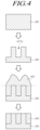
- FIG. 4 is a view illustrating an example of a process scheme of the polyimide substrate 300 according to various embodiments of the disclosure.
- the plurality of intaglio patterns EPTNs may be formed by etching a part of one surface of the polyimide substrate 300 .
- the intaglio pattern EPTN may be formed as a constant shape (e.g., each of the intaglio patterns EPTN may have a same or substantially the same shape as each other), a distance between the intaglio patterns EPTN may be constant (e.g., the distance between the intaglio patterns EPTN may be equally spaced apart).
- the filling 400 having a high transmittance and a certain coefficient of thermal expansion is disposed on one surface of the polyimide substrate 300 . Accordingly, the filling 400 may be disposed on one surface of the polyimide substrate 300 and be filled in the intaglio pattern EPTN formed on the polyimide substrate 300 .
- a top surface of the filling 400 disposed on the polyimide substrate 300 may be flatten by performing a planarization process like as a chemical mechanical polishing (CMP) process.
- CMP chemical mechanical polishing
- a top surface of the filling 400 may be positioned on a same plane with a top surface of a portion where the intaglio pattern EPTN is not disposed in a top surface of the polyimide substrate 300 (e.g., a top surface of the filling 400 may be coplanar or substantially coplanar with a top surface of a portion where the intaglio pattern EPTN is not disposed in a top surface of the polyimide substrate 300 ). That is, the top surface of the filling 400 may be flatten based on a portion where the intaglio pattern EPTN is not formed, it may be a shape that the filling 400 is filled in the intaglio pattern EPTN formed on the polyimide substrate 300 .
- a transmittance of the polyimide substrate 300 may be enhanced while maintaining a heat resistance of the polyimide substrate 300 .
- top surfaces of the polyimide substrate 300 and the filling 400 are flatten after the filling 400 is disposed on the polyimide substrate 300 , processes that insulation layers and various elements or the like are disposed on the polyimide substrate 300 which the intaglio pattern EPTN is formed may be performed easily.
- a planarization process may be performed for a part of the filling 400 to be disposed on a periphery area of the intaglio pattern EPTN on a top surface of the polyimide substrate 300 .
- FIG. 5 is a view illustrating other example of a structure of the polyimide substrate 300 according to various embodiments of the disclosure.
- the plurality of intaglio pattern EPTN may be disposed on at least a part area of the polyimide substrate 300 .
- the filling 400 may be disposed in the intaglio pattern EPTN of the polyimide substrate 300 .
- the filling 400 may be disposed on a periphery area of the intaglio pattern EPTN of the polyimide substrate 300 and be disposed on a top surface of the polyimide substrate 300 .
- the filling 400 may be disposed in the intaglio pattern EPTN of the polyimide substrate 300 and be disposed on the polyimide substrate 300 more.
- a structure that a part of the filling 400 is disposed on the polyimide substrate 300 may be formed.
- a transmittance of the filling 400 is higher than that of the polyimide substrate 300 , even though the filling 400 is disposed on the polyimide substrate 300 overall, an overall transmittance of the polyimide substrate 300 may not be reduced.
- a thickness of insulation layers disposed on the polyimide substrate 300 may be reduced as a part of the filling 400 is disposed on the polyimide substrate 300 .
- an insulation layer like as a buffer layer may be disposed on the polyimide substrate 300 before disposing an electrode layer constituting the thin film transistor on the polyimide substrate 300 .
- a thickness of the buffer layer disposed on the polyimide substrate 300 may be equal or greater than a certain thickness for a convenience of a process.
- a thickness of the buffer layer disposed on the polyimide substrate 300 may be reduced.
- a hardness of the polyimide substrate 300 may be weaken since a thickness of the polyimide substrate 300 on an area where the intaglio pattern EPTN is disposed is thin.
- a hardness of the polyimide substrate 300 may be compensated.
- a heat resistance of a polyimide substrate 300 may be maintained in a certain range while enhancing a transmittance of the polyimide substrate 300 .
- a shape of the intaglio pattern EPTN formed on the polyimide substrate 300 may be various. Furthermore, an area where the intaglio pattern EPTN is disposed may be various according to types of the display device 100 .
- FIGS. 6 A, 6 B, and 6 C are views illustrating an example of a shape of the intaglio pattern EPTN included in the polyimide substrate 300 according to various embodiments of the disclosure.
- FIGS. 6 A, 6 B, and 6 C illustrate an example of a plane structure that the filling 400 is disposed in the intaglio pattern EPTN formed on the polyimide substrate 300 and the filling 400 is flatten for top surfaces of the filling 400 and the polyimide substrate 300 to be positioned on a same plane.
- the plurality of intaglio pattern EPTN formed on one surface of the polyimide substrate 300 may have various shapes, but they may be formed as constant shapes on a same polyimide substrate 300 .
- the intaglio pattern EPTN formed on one surface of the polyimide substrate 300 may be a circle shape.
- the intaglio pattern EPTN formed on one surface of the polyimide substrate 300 may be a quadrangle shape.
- the intaglio pattern EPTN formed on one surface of the polyimide substrate 300 may be “L” shape.
- shapes of the intaglio pattern EPTN formed on one surface of the polyimide substrate 300 may be various.
- Shapes of the intaglio pattern EPTN formed on one surface of the polyimide substrate 300 may be configured variously considering a convenience of etching process, or a ratio of an area where the filling 400 is disposed, or the like.
- the plurality of the intaglio pattern EPTN may have same shapes to prevent that the intaglio pattern EPTN formed on the polyimide substrate 300 and the filling 400 disposed in the intaglio pattern EPTN are recognized as spots. Furthermore, distances between the intaglio pattern EPTN may be constant.
- shapes and distances of the intaglio pattern EPTN where the filling 400 is disposed on one surface of the polyimide substrate 300 may be configured to consider a process convenience and a transmittance or the like, they may be configured that the intaglio pattern EPTN having constant shapes is disposed on the polyimide substrate 300 as constant distances.
- the intaglio pattern EPTN formed on the polyimide substrate 300 may be disposed on the polyimide substrate 300 overall, in some cases, be disposed on a part area.
- FIGS. 7 and 8 are views illustrating examples of areas where the intaglio pattern EPTN is disposed in the polyimide substrate 300 according types of the display device 100 .
- FIG. 7 illustrates an example of an area where the intaglio pattern EPTN is disposed in a case that the display device 100 is a top emission structure
- FIG. 8 illustrates an example of an area where the intaglio pattern EPTN is disposed in a case that the display device 100 is a bottom emission structure.
- the light emitting portion EA and the circuit portion CA may be disposed to be overlapped in the subpixel SP to increase or maximize the transmission portion TA included in the subpixel SP.
- a light emitting element included in the light emitting portion EA may be positioned on a thin film transistor included in the circuit portion CA. And an area except for an area where the light emitting portion EA and the circuit portion CA are overlapped is an area where an element or the like is not disposed, and the area may constitute the transmission portion TA.
- the intaglio pattern EPTN formed on one surface of the polyimide substrate 300 may be positioned on an area overlapped to the transmission portion TA. And the intaglio pattern EPTN may not be positioned on an area overlapped to the light emitting portion EA and the circuit portion CA.
- the light emitting portion EA and the circuit portion CA are not areas to affect a transmittance of the display device 100 , even if the intaglio pattern EPTN where the filling 400 is disposed is not positioned on an area overlapped to the light emitting portion EA and the circuit portion CA, it may not affect the transmittance of the display device 100 .
- a transmittance of the display device 100 may be increased.
- a transmittance of the display device 100 may be improved while reducing or minimizing a process forming the intaglio pattern EPTN on the polyimide substrate 300 .
- the intaglio pattern EPTN of the polyimide substrate 300 is disposed on an area corresponding to the transmission portion TA only, a process for disposing the filling 400 in the intaglio pattern EPTN may not be performed.
- an inside of the intaglio pattern EPTN may be filled by insulation layers or the like disposed on a part area of the polyimide substrate 300 which the intaglio pattern EPTN is formed.
- a process for disposing insulation layers and various elements on that area may be performed.
- the intaglio pattern EPTN may be formed on an area corresponding to the transmission portion TA only, the filling 400 may be disposed in the intaglio pattern EPTN and a periphery area of the intaglio pattern EPTN.
- the filling 400 may be disposed also as a constant thickness on an area where the intaglio pattern EPTN is not disposed, such as an area corresponding to the light emitting portion EA and the circuit portion CA.
- the intaglio pattern EPTN may be formed overall on an area corresponding to the light emitting portion EA, the circuit portion CA and the transmission portion TA in the polyimide substrate 300 .
- the intaglio pattern EPTN is formed on the polyimide substrate 300 overall, as the filling 400 is disposed in the intaglio pattern EPTN, a process for disposing an element like as a thin film transistor on the polyimide substrate 300 may be performed easily.
- positions of a pattern area where the intaglio pattern EPTN is formed on one surface of the polyimide substrate 300 may be more various.
- the light emitting portion EA may not be overlapped with the circuit portion CA in each subpixel SP. That is, an opaque circuit portion CA may be positioned not to be overlapped with the light emitting portion EA, since a light emitted from the light emitting portion EA should be output through a bottom of the display device 100 .
- the transmission portion TA may be position on area except for an area where the light emitting portion EA and the circuit portion CA in the subpixel SP.
- the intaglio pattern EPTN formed on one surface of the polyimide substrate 300 may be positioned on an area overlapped with the transmission portion TA.
- the intaglio pattern EPTN may be positioned on an area overlapped with the transmission portion TA and the light emitting portion EA.
- the intaglio pattern EPTN may be positioned on the polyimide substrate 300 overall.
- a transmittance of the transmission portion TA may be increased by the intaglio pattern EPTN and the filling 400 filled in the intaglio pattern EPTN.
- a planarization process may be performed for a part of the filling 400 to be positioned on an area besides of the intaglio pattern EPTN.
- a thickness of an insulation layer disposed on the polyimide substrate 300 like as a buffer layer or the like, may be reduced, since the filling 400 is disposed on the light emitting portion EA, the circuit portion CA and the transmission portion TA overall.
- a transmittance of an area corresponding to the light emitting portion EA of the subpixel SP may be increased also, an efficiency of a light emitted through a bottom of the polyimide substrate 300 may be increased also.
- a transmittance of the display device 100 may be improved by increasing a transmittance of the polyimide substrate 300 , and at the same time, a light efficiency of the display device 100 having a structure that a light is emitted through the polyimide substrate 300 may be enhanced also.
- a process may be simplified by forming the intaglio pattern EPTN on the polyimide substrate 300 overall.
- a transmittance of the polyimide substrate 300 may be increased.
- a heat resistance of the polyimide substrate 300 may be maintained while increasing a transmittance of the polyimide substrate 300 .
- elements that a high temperature heat process is required may be disposed on the polyimide substrate 300 which increases a transmittance of the polyimide substrate 300 .
- a thickness of an insulation layer or the like disposed on the polyimide substrate 300 may be reduced.
- the intaglio pattern EPTN of the polyimide substrate 300 is disposed on an area corresponding to the transmission portion TA only, or is disposed on an area corresponding to the light emitting portion EA more, a transmittance or a light efficiency of the display device 100 may be improved.
Abstract
Description
Claims (20)
Applications Claiming Priority (2)
| Application Number | Priority Date | Filing Date | Title |
|---|---|---|---|
| KR10-2019-0165224 | 2019-12-12 | ||
| KR1020190165224A KR20210074494A (en) | 2019-12-12 | 2019-12-12 | Polyimide substrate and display device |
Publications (2)
| Publication Number | Publication Date |
|---|---|
| US20210183904A1 US20210183904A1 (en) | 2021-06-17 |
| US11646319B2 true US11646319B2 (en) | 2023-05-09 |
Family
ID=76317053
Family Applications (1)
| Application Number | Title | Priority Date | Filing Date |
|---|---|---|---|
| US17/109,941 Active 2041-03-25 US11646319B2 (en) | 2019-12-12 | 2020-12-02 | Polyimide substrate including intaglio patterns and display device including the same |
Country Status (3)
| Country | Link |
|---|---|
| US (1) | US11646319B2 (en) |
| KR (1) | KR20210074494A (en) |
| CN (1) | CN112992974A (en) |
Citations (18)
| Publication number | Priority date | Publication date | Assignee | Title |
|---|---|---|---|---|
| JPS62200324A (en) | 1986-02-28 | 1987-09-04 | Fujitsu Ltd | Projection type liquid crystal display device |
| US5972193A (en) * | 1997-10-10 | 1999-10-26 | Industrial Technology Research Institute | Method of manufacturing a planar coil using a transparency substrate |
| US6118586A (en) * | 1995-10-03 | 2000-09-12 | Asahi Glass Company Ltd. | Optical head device including an optically anisotropic diffraction grating and production method thereof |
| US6549105B2 (en) * | 1998-06-02 | 2003-04-15 | Matsushita Electric Industrial Co., Ltd. | Millimeter wave module and radio apparatus |
| US20050202348A1 (en) * | 2004-03-11 | 2005-09-15 | Canon Kabushiki Kaisha | Substrate, conductive substrate, fine structure substrate, organic field effect transistor and manufacturing method thereof |
| KR20080060794A (en) | 2006-12-27 | 2008-07-02 | 삼성전자주식회사 | Array substrate and colorfilter substrate, liquid crystal display having the same and method of fabricating the same |
| US20140175405A1 (en) * | 2012-12-22 | 2014-06-26 | Industrial Technology Research Institute | Electronic device package structure and manufacturing method thereof |
| US20160204365A1 (en) * | 2013-12-04 | 2016-07-14 | Lg Chem, Ltd. | Method of manufacturing substrate for organic electronic device |
| KR20160096760A (en) | 2015-02-05 | 2016-08-17 | 삼성디스플레이 주식회사 | Transparent display substrates, transparent display devices and methods of manufacturing transparent display devices |
| US20170194392A1 (en) * | 2016-01-05 | 2017-07-06 | Boe Technology Group Co., Ltd. | Electroluminescent display panel, fabricating method thereof and display device |
| US20180149904A1 (en) * | 2016-11-30 | 2018-05-31 | Lg Display Co., Ltd. | Cover window and foldable display device including the same |
| US20180287099A1 (en) * | 2015-09-10 | 2018-10-04 | Sharp Kabushiki Kaisha | Organic electroluminescence device, method for manufacturing organic electroluminescence device, illumination device, and display device |
| US20180323404A1 (en) * | 2015-11-16 | 2018-11-08 | Sharp Kabushiki Kaisha | Organic electroluminescence device, production method for organic electroluminescence device, illumination device and display device |
| US20190067575A1 (en) * | 2017-08-25 | 2019-02-28 | Wuhan China Star Optoelectronics Semiconductor Display Technology Co., Ltd. | Method of manufacturing flexible display panel |
| US20190229229A1 (en) * | 2018-01-25 | 2019-07-25 | Primax Electronics Ltd. | Light source module |
| US20200132989A1 (en) * | 2018-10-31 | 2020-04-30 | Samsung Display Co., Ltd. | Foldable display device |
| US20210367199A1 (en) * | 2018-05-11 | 2021-11-25 | Yungu (Gu' An) Technology Co., Ltd. | Display screen and method of manufacturing thereof |
| US11543703B2 (en) * | 2018-12-11 | 2023-01-03 | Innolux Corporation | Display apparatus |
Family Cites Families (5)
| Publication number | Priority date | Publication date | Assignee | Title |
|---|---|---|---|---|
| US10263203B2 (en) * | 2016-12-30 | 2019-04-16 | Lg Display Co., Ltd. | Display device |
| KR102378879B1 (en) * | 2017-08-28 | 2022-03-24 | 엘지디스플레이 주식회사 | Flexible color filter substrate and flexible light emitting display apparatus comprising the same |
| CN107527998B (en) * | 2017-08-30 | 2020-07-03 | 武汉华星光电半导体显示技术有限公司 | Flexible substrate, flexible OLED device and preparation method thereof |
| KR102524429B1 (en) * | 2017-10-31 | 2023-04-20 | 엘지디스플레이 주식회사 | Transparent display apparatus |
| CN109360849B (en) * | 2018-11-01 | 2021-01-29 | 京东方科技集团股份有限公司 | Substrate, manufacturing method thereof and transparent display device |
-
2019
- 2019-12-12 KR KR1020190165224A patent/KR20210074494A/en active Search and Examination
-
2020
- 2020-11-30 CN CN202011370595.1A patent/CN112992974A/en active Pending
- 2020-12-02 US US17/109,941 patent/US11646319B2/en active Active
Patent Citations (20)
| Publication number | Priority date | Publication date | Assignee | Title |
|---|---|---|---|---|
| JPS62200324A (en) | 1986-02-28 | 1987-09-04 | Fujitsu Ltd | Projection type liquid crystal display device |
| US6118586A (en) * | 1995-10-03 | 2000-09-12 | Asahi Glass Company Ltd. | Optical head device including an optically anisotropic diffraction grating and production method thereof |
| US5972193A (en) * | 1997-10-10 | 1999-10-26 | Industrial Technology Research Institute | Method of manufacturing a planar coil using a transparency substrate |
| US6549105B2 (en) * | 1998-06-02 | 2003-04-15 | Matsushita Electric Industrial Co., Ltd. | Millimeter wave module and radio apparatus |
| US20050202348A1 (en) * | 2004-03-11 | 2005-09-15 | Canon Kabushiki Kaisha | Substrate, conductive substrate, fine structure substrate, organic field effect transistor and manufacturing method thereof |
| KR20080060794A (en) | 2006-12-27 | 2008-07-02 | 삼성전자주식회사 | Array substrate and colorfilter substrate, liquid crystal display having the same and method of fabricating the same |
| US8040477B2 (en) | 2006-12-27 | 2011-10-18 | Samsung Electronics Co., Ltd. | Array substrate, liquid crystal display panel, and method of manufacturing the same |
| US20140175405A1 (en) * | 2012-12-22 | 2014-06-26 | Industrial Technology Research Institute | Electronic device package structure and manufacturing method thereof |
| US20160204365A1 (en) * | 2013-12-04 | 2016-07-14 | Lg Chem, Ltd. | Method of manufacturing substrate for organic electronic device |
| US9634074B2 (en) | 2015-02-05 | 2017-04-25 | Samsung Display Co., Ltd. | Transparent display substrates, transparent display devices and methods of manufacturing transparent display devices |
| KR20160096760A (en) | 2015-02-05 | 2016-08-17 | 삼성디스플레이 주식회사 | Transparent display substrates, transparent display devices and methods of manufacturing transparent display devices |
| US20180287099A1 (en) * | 2015-09-10 | 2018-10-04 | Sharp Kabushiki Kaisha | Organic electroluminescence device, method for manufacturing organic electroluminescence device, illumination device, and display device |
| US20180323404A1 (en) * | 2015-11-16 | 2018-11-08 | Sharp Kabushiki Kaisha | Organic electroluminescence device, production method for organic electroluminescence device, illumination device and display device |
| US20170194392A1 (en) * | 2016-01-05 | 2017-07-06 | Boe Technology Group Co., Ltd. | Electroluminescent display panel, fabricating method thereof and display device |
| US20180149904A1 (en) * | 2016-11-30 | 2018-05-31 | Lg Display Co., Ltd. | Cover window and foldable display device including the same |
| US20190067575A1 (en) * | 2017-08-25 | 2019-02-28 | Wuhan China Star Optoelectronics Semiconductor Display Technology Co., Ltd. | Method of manufacturing flexible display panel |
| US20190229229A1 (en) * | 2018-01-25 | 2019-07-25 | Primax Electronics Ltd. | Light source module |
| US20210367199A1 (en) * | 2018-05-11 | 2021-11-25 | Yungu (Gu' An) Technology Co., Ltd. | Display screen and method of manufacturing thereof |
| US20200132989A1 (en) * | 2018-10-31 | 2020-04-30 | Samsung Display Co., Ltd. | Foldable display device |
| US11543703B2 (en) * | 2018-12-11 | 2023-01-03 | Innolux Corporation | Display apparatus |
Also Published As
| Publication number | Publication date |
|---|---|
| CN112992974A (en) | 2021-06-18 |
| US20210183904A1 (en) | 2021-06-17 |
| KR20210074494A (en) | 2021-06-22 |
Similar Documents
| Publication | Publication Date | Title |
|---|---|---|
| KR102414940B1 (en) | Display device and method of manufacturing the same | |
| US10930723B2 (en) | Display device | |
| KR102281226B1 (en) | Display device | |
| US11437439B2 (en) | Display device | |
| EP3671852B1 (en) | Organic light emitting display panel and organic light emitting display device including the same | |
| CN110737348A (en) | Display device with touch sensor | |
| US11901371B2 (en) | Contact structure and display device including the same | |
| CN105096753A (en) | Array base plate, manufacturing method of array base plate and display device | |
| US20220399473A1 (en) | Method of manufacturing display device | |
| CN107026188B (en) | Color filter substrate and display device having the same | |
| EP3671850A1 (en) | Organic light emitting display panel and organic light emitting display device including the same | |
| US11385515B2 (en) | Display device | |
| CN110391278B (en) | Electroluminescent display device with improved contact structure | |
| US11646319B2 (en) | Polyimide substrate including intaglio patterns and display device including the same | |
| US20210408078A1 (en) | Electronic Device Substrate, Manufacturing Method Thereof, and Electronic Device | |
| KR20210083917A (en) | Display apparatus | |
| KR20200134908A (en) | Display panel | |
| US20230157054A1 (en) | Display device | |
| US11880523B2 (en) | Touch display device and gate driving circuit | |
| KR102486147B1 (en) | Thin film transistor array substrate and electronic device including the same | |
| US20230004258A1 (en) | Transparent touch display device | |
| US20230380225A1 (en) | Touch display device | |
| US20240045540A1 (en) | Touch display device | |
| KR102512779B1 (en) | Electroluminescent display device | |
| US20230207537A1 (en) | Display device |
Legal Events
| Date | Code | Title | Description |
|---|---|---|---|
| FEPP | Fee payment procedure |
Free format text: ENTITY STATUS SET TO UNDISCOUNTED (ORIGINAL EVENT CODE: BIG.); ENTITY STATUS OF PATENT OWNER: LARGE ENTITY |
|
| AS | Assignment |
Owner name: LG DISPLAY CO., LTD., KOREA, REPUBLIC OF Free format text: ASSIGNMENT OF ASSIGNORS INTEREST;ASSIGNORS:KIM, SUNGHOON;SHIN, DONGCHAE;SON, KYUNGMO;REEL/FRAME:055686/0953 Effective date: 20201103 |
|
| STPP | Information on status: patent application and granting procedure in general |
Free format text: APPLICATION DISPATCHED FROM PREEXAM, NOT YET DOCKETED |
|
| STPP | Information on status: patent application and granting procedure in general |
Free format text: DOCKETED NEW CASE - READY FOR EXAMINATION |
|
| STPP | Information on status: patent application and granting procedure in general |
Free format text: NON FINAL ACTION MAILED |
|
| STPP | Information on status: patent application and granting procedure in general |
Free format text: RESPONSE TO NON-FINAL OFFICE ACTION ENTERED AND FORWARDED TO EXAMINER |
|
| STPP | Information on status: patent application and granting procedure in general |
Free format text: FINAL REJECTION MAILED |
|
| STCF | Information on status: patent grant |
Free format text: PATENTED CASE |