US7986394B2 - Flexural liquid crystal panel and liquid crystal device - Google Patents
Flexural liquid crystal panel and liquid crystal device Download PDFInfo
- Publication number
- US7986394B2 US7986394B2 US12/001,401 US140107A US7986394B2 US 7986394 B2 US7986394 B2 US 7986394B2 US 140107 A US140107 A US 140107A US 7986394 B2 US7986394 B2 US 7986394B2
- Authority
- US
- United States
- Prior art keywords
- substrate
- liquid crystal
- crystal panel
- horizontal direction
- color filter
- Prior art date
- Legal status (The legal status is an assumption and is not a legal conclusion. Google has not performed a legal analysis and makes no representation as to the accuracy of the status listed.)
- Active, expires
Links
Images


Classifications
-
- G—PHYSICS
- G02—OPTICS
- G02F—OPTICAL DEVICES OR ARRANGEMENTS FOR THE CONTROL OF LIGHT BY MODIFICATION OF THE OPTICAL PROPERTIES OF THE MEDIA OF THE ELEMENTS INVOLVED THEREIN; NON-LINEAR OPTICS; FREQUENCY-CHANGING OF LIGHT; OPTICAL LOGIC ELEMENTS; OPTICAL ANALOGUE/DIGITAL CONVERTERS
- G02F1/00—Devices or arrangements for the control of the intensity, colour, phase, polarisation or direction of light arriving from an independent light source, e.g. switching, gating or modulating; Non-linear optics
- G02F1/01—Devices or arrangements for the control of the intensity, colour, phase, polarisation or direction of light arriving from an independent light source, e.g. switching, gating or modulating; Non-linear optics for the control of the intensity, phase, polarisation or colour
- G02F1/13—Devices or arrangements for the control of the intensity, colour, phase, polarisation or direction of light arriving from an independent light source, e.g. switching, gating or modulating; Non-linear optics for the control of the intensity, phase, polarisation or colour based on liquid crystals, e.g. single liquid crystal display cells
- G02F1/133—Constructional arrangements; Operation of liquid crystal cells; Circuit arrangements
- G02F1/1333—Constructional arrangements; Manufacturing methods
- G02F1/133305—Flexible substrates, e.g. plastics, organic film
-
- G—PHYSICS
- G02—OPTICS
- G02F—OPTICAL DEVICES OR ARRANGEMENTS FOR THE CONTROL OF LIGHT BY MODIFICATION OF THE OPTICAL PROPERTIES OF THE MEDIA OF THE ELEMENTS INVOLVED THEREIN; NON-LINEAR OPTICS; FREQUENCY-CHANGING OF LIGHT; OPTICAL LOGIC ELEMENTS; OPTICAL ANALOGUE/DIGITAL CONVERTERS
- G02F1/00—Devices or arrangements for the control of the intensity, colour, phase, polarisation or direction of light arriving from an independent light source, e.g. switching, gating or modulating; Non-linear optics
- G02F1/01—Devices or arrangements for the control of the intensity, colour, phase, polarisation or direction of light arriving from an independent light source, e.g. switching, gating or modulating; Non-linear optics for the control of the intensity, phase, polarisation or colour
- G02F1/13—Devices or arrangements for the control of the intensity, colour, phase, polarisation or direction of light arriving from an independent light source, e.g. switching, gating or modulating; Non-linear optics for the control of the intensity, phase, polarisation or colour based on liquid crystals, e.g. single liquid crystal display cells
- G02F1/133—Constructional arrangements; Operation of liquid crystal cells; Circuit arrangements
- G02F1/1333—Constructional arrangements; Manufacturing methods
- G02F1/133368—Cells having two substrates with different characteristics, e.g. different thickness or material
Definitions
- the invention relates to an active matrix type liquid crystal panel and an active matrix type liquid crystal display device.
- the picture of the liquid crystal display device changes to large picture has been speeded up as the liquid crystal display device is used as the display device of the television set.
- the viewer has discovered that a problem exists, in which the visual angle difference existing between the visual angle for viewing the central part of the picture and the visual angle for viewing the right and left ends of the picture (the term “visual angle” is defined as an angle formed by the visual line of the observer who views the picture and the tangent of the picture, and the difference value is defined as the “visual angle difference”) will be greater.
- the shape of the flexural panel is formed in a concave shape at a side near the observer is taken into consideration.
- the liquid crystal panel is formed by two glass sheet having the liquid crystal sandwiched between them, therefore, by setting the position of the observer's eye as a center, if two glass sheet are bent in a concave shape at the observer's side, then a tender difference exists between the width of the glass substrate near the observer's side, that is, at the inner side, and the width of the glass substrate at the far end, that is, at the outer side, the width of the glass in a transverse direction at the outer side will be wider. This will be described with reference to the following drawings.
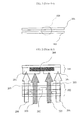
- FIG. 10 is a simplified cross sectional view of the glass substrates before two sheets of the substrates being bent.
- FIG. 11 is a simplified cross sectional view of the glass substrate after two sheets of the substrates being bent.
- 101 is a CF (Color Filter) substrate of the two sheets of the substrates which is the nearest one to the observer
- 102 is a TFT (Thin Film Transistor) substrate which is the farthest one to the observer
- 110 is an arrow indicating the sight line of the observer.
- the width of the outer substrate must be larger than the transverse width of the inner substrate.
- FIG. 1 is a cross sectional view of a plan liquid crystal panel.
- FIG. 2 is an enlarged cross sectional view of a portion 103 in FIG. 1 .
- 204 is a black matrix (Hereinafter also referred to as “BM”)
- 201 is a pigmentation section of the color filter
- 202 is a signal line
- 205 is a light of the back-lighting transmitted to BM 204
- 206 is a light of the back-lighting transmitted to the pigmentation section 201
- 203 is ITO (Indium Tin Oxide) of the pixel.
- the light cannot pass through BM 204 so that BM 204 may block the light 205 , and it cannot reach the eyes of the observer.
- the signal line 202 can be hidden at the back of BM 204 and cannot be seen by the eyes of the observer.
- ITO 203 is transparent, the light 206 is transformed into color light after passing through the pigmentation section 201 , and then reaches the eyes of the observer, and the observer can view a correct image.
- FIG. 3 is a cross sectional view of a substrate which is a substrate of two sheets of plan substrates shown in FIG. 1 after bending.
- FIG. 4 is an enlarged sectional view of the section 301 shown in FIG. 3 .
- the light 205 of FIG. 4 is a light which is blocked actually by BM 204 , however, the panel is bent so that the position of BM 204 is slightly different from that of the liquid crystal panel in a plan shape, therefore the light leaks from the adjacent pigmentation section 201 .
- the CF substrate and TFT substrate in FIG. 4 are flexural rather than in the plan shape, however, it is an enlarged view so that the flexuosity is very small and it can be described as a plane.
- JP58-52513 The reference, Japanese Utility Publication No. JP58-52513, is incorporated by reference in its entirety.
- the object of the invention is to provide a liquid crystal display device having flexural panel, which is formed by bending the normal plan liquid crystal panel, and it is a liquid crystal display device having flexural panel with an excellent display quality that no any light leaks out.
- the liquid crystal panel according to the first aspect of the invention is formed by sandwiching the liquid crystal between a TFT substrate and a CF substrate, said TFT substrate has the pixels containing the thin film transistors disposed in a matrix shape, and said CF substrate has color filter, wherein:
- said entire liquid crystal panel is bent so that one side of the liquid crystal which facing the observer presents a concave shape
- the length at the horizontal direction of the effective display region on the substrate, which is located near the observer's side, is shorter than the length at the horizontal direction of the effective display region on the substrate, which is located far from the observer's side.
- the leakage of the light can be prevented from occurring by adjusting the difference between the arc length of the inner substrate and the arc length of the outer substrate.
- a liquid crystal panel according to the second aspect is a liquid crystal panel according to the first aspect, wherein said substrate, which is located near the observer's side, is the color filter substrate; said substrate, which is located far from the observer's side, is the thin film transistor substrate.
- a liquid crystal panel according to the third aspect is a liquid crystal panel according to the second aspect, wherein the pitch at a horizontal direction between the respective pixels on said CF substrate is smaller than the pitch at a horizontal direction between the respective pixels on said TFT substrate.
- the light leakage caused by the position offset of the black matrix of the color filter can be prevented from occurring by adjusting the pitch of the respective pixels.
- a liquid crystal panel according to the fourth aspect is formed by sandwiching the liquid crystal between the TFT substrate having the pixels containing the thin film transistors disposed in a matrix shape and the CF substrate having the color filter, wherein:
- said entire liquid crystal panel is bent so that one side of the liquid crystal which facing the observer presents a concave shape
- the width at the horizontal direction of a black matrix existing in both left and right end regions at the horizontal direction of the substrate, which is located near the observer's side, is wider than the width of a black matrix on the center section region of the same substrate.
- a liquid crystal panel according to the fifth aspect is a liquid crystal panel according to the fourth aspect, wherein said substrate, which is located near the observer's side, is a color filter substrate.
- a liquid crystal panel according to the sixth aspect is a liquid crystal panel according to the fourth aspect, wherein the pitch at a horizontal direction between the respective pixels on said CF substrate is equal to the pitch at a horizontal direction between the respective pixels on said TFT substrate.
- the width at the horizontal direction of the black matrix is changed to allow the pitch of the pixels on the CF substrate to be equal to the pitch of the pixels on the TFT substrate thereby the same liquid crystal panel can be used commonly for the plan liquid crystal panel and the flexural liquid crystal panel.
- a liquid crystal panel according to the seventh aspect is a liquid crystal panel according to the fifth aspect, wherein the pitch at a horizontal direction between the respective pixels on said color filter substrate is smaller than or equal to the pitch at a horizontal direction between the respective pixels on said thin film transistor substrate.
- a liquid crystal display device wherein it comprises the liquid crystal panel as described at any aspect of the above first ⁇ seventh aspects.
- a flexural panel display device which is constructed by bending a normal plan liquid crystal panel, will be provided, and a flexural liquid crystal panel display device is formed by bending the plan liquid crystal panel so as to prevent the light of the back lighting from leaking, and having an excellent display quality.
- FIG. 1 is a cross sectional view of a plan liquid crystal panel.
- FIG. 2 is an enlarged cross sectional of a portion 103 in FIG. 1 .
- FIG. 3 is a cross sectional view of a substrate formed after bending the two sheets of the plan substrates in FIG. 1 .
- FIG. 4 is an enlarged cross sectional view of a portion 301 in FIG. 3 .
- FIG. 5 is a cross sectional view showing a state before bending the CF substrate and TFT substrate when the pitch at the horizontal direction of the respective pixels on the CF substrate and the pitch at the horizontal direction of the respective pixels on the TFT substrate are the same, and the side lengths at the horizontal direction of the CF substrate and the TFT substrate are the same.
- FIG. 6 is a cross sectional view after the substrates shown in FIG. 5 being bent.
- FIG. 7 is a cross sectional view of the CF substrate and TFT substrate in the plan shape before forming the flexural shape, and characterized in that the pitch at the left to right direction of the pixels on the CF substrate is shorter than the pitch of the pixels on the TFT substrate.
- FIG. 8 is a cross sectional view of the panel in FIG. 7 after bending.
- FIG. 9 is a view used for describing a calculation method.
- FIG. 10 is a view of the glass substrates in which the outline of the two sheets of the substrates before bending is viewed from an end direction of the substrate.
- FIG. 11 is a simplified cross sectional view of the two sheets of the substrates in FIG. 10 after bending.
- FIG. 12 is a deploying perspective view indicating a liquid crystal panel manufacturing method in which the pitch are disposed to change a plan shape liquid crystal panel to a flexural shape liquid crystal panel.
- FIG. 13 is a cross sectional view of a substrate under a condition that the width of BM existing near both the left and right ends of the CF substrate and the width of BM existing in the center are the same.
- FIG. 14 is a cross sectional view of a liquid crystal panel, the flexural shape of which is formed by bending the panel in FIG. 13 .
- FIG. 15 is a cross sectional view of a substrate of the liquid crystal panel substrate before it is bent according to an embodiment of the invention.
- FIG. 16 is a cross sectional view of a liquid crystal panel having a flexural shape after bending the panel in FIG. 15 .
- a flexural liquid crystal panel according to the Embodiment I of the invention in the two sheets of the substrates forming the liquid crystal panel, the pitch at the left-to-right direction of the respective pixels on the substrate which is located near the observer's side, that is, the CF substrate, is shorter than the pitch of the respective pixels on the substrate which is located far from the observer's side.
- FIG. 7 is a cross sectional view of the CF substrate and TFT substrate in the plan shape before forming the flexural shape, and characterized in that the pitch at the left-to-right direction of the pixels on the CF substrate is shorter than the pitch of the pixels on the TFT substrate.
- 101 is a CF substrate
- 102 is a TFT substrate
- 204 is a BM
- 704 is the position of BM when the pitch of the respective pixels on the CF substrate and the pitch of the respective pixels on the TFT substrate are assumed to be the same.
- the pitch at the left to right direction of the respective pixels on the CF substrate is formed to be shorter than the pitch of the respective pixels on the TFT substrate.
- the BM existing near both left and right ends on the CF substrate is located slightly adjacent to the center, as shown in FIG. 7 .
- the photo mask having different pixel pitch is not used for the CF substrate and the TFT substrate, rather, the photo mask having the same pitch is used, when the process, such as the exposal process, and the like, is performed, if the exposal on the CF substrate and TFT substrate is performed by changing the magnification, then the photo mask which is the same as the photo mask used in the prior art can be used to manufacture the flexural liquid crystal panel of the Embodiment 1.
- a bend method for bending a plan panel in order to form a concave shape at the observer's side will be described as follows.
- the liquid crystal panel is fixed by the spacer which are formed in a flexural shape, for example, at two sides at a horizontal direction viewed by the observer of the liquid crystal among four sides around the plan shape panel, meanwhile, the liquid crystal panel is assembled into the liquid crystal display device thereby the plan shape panel is bent. It will be described according to the drawings as follows.
- FIG. 12 is a deploying perspective view of the respective components indicating a liquid crystal panel manufacturing method in which the spacers are disposed to change a plan shape liquid crystal panel to a flexural shape liquid crystal panel.
- 1201 is a spacer having convex shape
- 1207 is a spacer having flexural shape in concave shape
- 101 is a CF substrate
- 102 is a TFT substrate
- 1208 is a back lighting unit.
- the spacers 1207 and 1201 By using the spacers 1207 and 1201 to hold the CF substrate and the TFT substrate, because the CF substrate and the TFT substrate are very thin, so they turn into a flexural shape by bending them simply.
- the manufacturing method in FIG. 12 is only an example.
- FIG. 8 is a cross sectional view of the liquid crystal panel according to the Embodiment 1 of the invention after the shape of the panel turning to a flexural shape.
- 204 is a BM
- 101 is a CF substrate
- 103 is a TFT substrate.
- the pitch at the horizontal direction of the respective pixels on the CF substrate is shorter than the pitch at the horizontal direction of the respective pixels on the TFT substrate.
- the length of the side at the horizontal direction of the CF substrate is shorter than the length of the side at the horizontal direction of the TFT substrate.
- FIG. 5 is a cross sectional view indicating the relative position relation between the position of BM 204 and the signal line 202 when the pitch at the horizontal direction of the respective pixels on the CF substrate and the pitch at the horizontal direction of the respective pixels on the TFT substrate are the same.
- FIG. 6 is a cross sectional view showing the substrates shown in FIG. 5 being bent.
- K is the light from the back lighting. If the pitch at the horizontal direction of the respective pixels on the CF substrate and the pitch at the horizontal direction of the respective pixels on the TFT substrate are the same, then the light K, which can be masked originally by BM 204 , will leak as shown in FIG. 6 . Further, the signal line 202 cannot be hidden behind the BM.
- a substrate structure is formed in which the observer's side of the flexural liquid crystal panel, that is the CF substrate side, of the Embodiment 2 is bent to a concave shape to allow the pitch of the pixels on the CF substrate to be the same as the pitch of the pixels on the TFT substrate, however, the width at the left to right direction of the black matrix existing in both the left and right end regions of the CF substrate bending in a concave shape is wider than the width at the left-to-right direction of the black matrix disposed in the central section region.
- FIG. 15 is a cross sectional view of a substrate of the liquid crystal panel substrate before it is bent according the Embodiment 2 of the invention.
- 101 is a CF substrate
- 102 is a TFT substrate
- 204 is BM.
- the width of the BM existing near both left and right ends of the CF substrate is wider than the width of the BM existing in the center. The shape formed after bending the substrate will be described as follows.
- FIG. 16 is a cross sectional view of a liquid crystal panel having a flexural shape after bending the panel in FIG. 15 .
- 204 is BM
- 101 is a CF substrate
- 102 is a TFT substrate.
- FIG. 13 is a cross sectional view of a substrate under a condition that the width of BM existing near both the left and right ends of the CF substrate and the width of BM existing in the center are the same.
- FIG. 14 is a cross sectional view of a liquid crystal panel having a flexural shape when the panel in FIG. 15 is bent.
- K is the light coming from the back lighting.
- the width of BM existing near both the left and right ends of the CF substrate and the width of BM existing in the center are the same, then the light K which can be masked originally by BM 204 will leak out. Further, the signal line 202 cannot be hidden behind BM.
- the width of BM existing near both the left and right ends of the CF substrate is wider than the width of BM existing in the center.
- the light K is masked by BM 204 , therefore, the light does not leak out.
- the signal line 202 can hide behind BM 204 . As a result, an excellent display quality can be obtained.
- the flexural liquid crystal panel of the Embodiment 2 of the invention is: for the flexural liquid crystal panel of the Embodiment 2, the leakage of the light can be prevented not only under the condition that the panel is bent, but also under the condition that it is a plan panel. That is, the liquid crystal panel of the Embodiment 2 of the invention can be used for both plan liquid crystal panel and flexural liquid crystal panel.
- the flexural liquid crystal panel of the Embodiment 2 of the invention except that it has a characteristic that the width at the left-to-right direction of the black matrix existing in both left and right end regions of the CF substrate having a concave shape bend is wider than the width at the left to right direction of the black matrix disposing in the central section region, it also has another characteristic that the pitch of the pixels on the CF substrate and the pitch of the pixels on the TFT substrate are the same; however, as another embodiment of the invention, it has a characteristic that the width at the horizontal direction (left to right direction) of the black matrix existing in both left and right end regions of the CF substrate having a concave shape bend is wider than the width at the left to right direction of the black matrix disposing in the central section region, and also comprises a characteristic that the pitch at the horizontal direction (left-to-right direction) of the pixels on the CF substrate is smaller than the pitch at the horizontal direction (left-to-right direction) of the pixels on the TFT substrate.
- the structure of the liquid crystal panel of said embodiment synthesizes the features of the Embodiment 1 and Embodiment 2, the specific description is omitted herein and so is the method for bending the plan liquid crystal panel.
- the transverse length is 1042 mm
- the longitudinal length is 586 mm
- the gap between the CF substrate and TFT substrate is 5 ⁇ m
- the distance between the position of the observer's eyes and the panel is 1650 mm.
- FIG. 9 is a view used for describing a calculation method of the example.
- 101 is a CF substrate
- 102 is a TFT substrate
- 701 is a gap for sandwiching the liquid crystal
- W is the length of the gap 701
- 702 is an arc at the outer side of the gap 701
- ⁇ is an angle between a line connecting the eyes of the observer with the left end of the TV panel and a line connecting the eyes of the observer with the right end of the TV panel.
- W is 5 ⁇ m.
- the cross sectional view is not a simple shape as shown in FIG. 9 because of the internal stress of the substrates.
- the purpose of FIG. 9 is to describe a formula for calculating the difference between the arc 701 and the arc 702 , therefore it is not correct, but only for the convenience for describing.
- ⁇ can be calculated with the following formula (1).
Landscapes
- Physics & Mathematics (AREA)
- Nonlinear Science (AREA)
- Mathematical Physics (AREA)
- Chemical & Material Sciences (AREA)
- Crystallography & Structural Chemistry (AREA)
- General Physics & Mathematics (AREA)
- Optics & Photonics (AREA)
- Liquid Crystal (AREA)
- Devices For Indicating Variable Information By Combining Individual Elements (AREA)
Applications Claiming Priority (2)
| Application Number | Priority Date | Filing Date | Title |
|---|---|---|---|
| JP2006333625A JP5026777B2 (ja) | 2006-12-11 | 2006-12-11 | 湾曲液晶パネル及び液晶表示装置 |
| JP2006-333625 | 2006-12-11 |
Publications (2)
| Publication Number | Publication Date |
|---|---|
| US20080137013A1 US20080137013A1 (en) | 2008-06-12 |
| US7986394B2 true US7986394B2 (en) | 2011-07-26 |
Family
ID=39497547
Family Applications (1)
| Application Number | Title | Priority Date | Filing Date |
|---|---|---|---|
| US12/001,401 Active 2029-10-23 US7986394B2 (en) | 2006-12-11 | 2007-12-11 | Flexural liquid crystal panel and liquid crystal device |
Country Status (3)
| Country | Link |
|---|---|
| US (1) | US7986394B2 (ja) |
| JP (1) | JP5026777B2 (ja) |
| CN (1) | CN101201486B (ja) |
Cited By (6)
| Publication number | Priority date | Publication date | Assignee | Title |
|---|---|---|---|---|
| US8477271B2 (en) | 2008-12-26 | 2013-07-02 | Sharp Kabushiki Kaisha | Liquid crystal display device |
| US20160139457A1 (en) * | 2014-11-14 | 2016-05-19 | Shenzhen China Star Optoelectronics Technology Co., Ltd. | Curved liquid crystal display panel and curved liquid crystal display apparatus |
| US10114242B2 (en) | 2012-12-13 | 2018-10-30 | 3M Innovative Properties Company | Curved automatic-darkening filter |
| US10663788B2 (en) | 2016-11-16 | 2020-05-26 | Mitsubishi Electric Corporation | Liquid crystal display and method of manufacturing liquid crystal display |
| US10712596B2 (en) | 2013-08-02 | 2020-07-14 | Samsung Display Co., Ltd. | Liquid crystal display |
| US11226513B2 (en) | 2018-09-19 | 2022-01-18 | Ordos Yuansheng Optoelectronics Co., Ltd. | Curved display panel, manufacturing method thereof and display device |
Families Citing this family (49)
| Publication number | Priority date | Publication date | Assignee | Title |
|---|---|---|---|---|
| JP5322427B2 (ja) * | 2007-12-19 | 2013-10-23 | 三菱電機株式会社 | 液晶表示装置 |
| JP5123078B2 (ja) * | 2008-06-30 | 2013-01-16 | 三菱電機株式会社 | 液晶表示装置及び製造方法 |
| TWI433071B (zh) * | 2009-09-22 | 2014-04-01 | Ind Tech Res Inst | 三維曲面顯示裝置、其製造方法及可塑性顯示面板 |
| KR101907165B1 (ko) * | 2012-09-14 | 2018-10-15 | 삼성전자주식회사 | 곡면형 디스플레이 장치 |
| US20160026035A1 (en) | 2013-03-15 | 2016-01-28 | Sony Corporation | Display device and method of manufacturing the same |
| KR102159739B1 (ko) * | 2013-08-02 | 2020-09-25 | 삼성디스플레이 주식회사 | 액정표시장치 |
| US20150055063A1 (en) * | 2013-08-23 | 2015-02-26 | Innolux Corporation | Display apparatus |
| CN103605228B (zh) * | 2013-11-27 | 2016-09-07 | 青岛海信电器股份有限公司 | 显示设备和液晶电视机 |
| KR102243856B1 (ko) | 2014-04-07 | 2021-04-26 | 삼성디스플레이 주식회사 | 표시 장치 |
| CN104050882B (zh) | 2014-05-30 | 2016-07-20 | 京东方科技集团股份有限公司 | 一种显示装置 |
| KR102152178B1 (ko) * | 2014-06-13 | 2020-09-07 | 엘지디스플레이 주식회사 | 곡면 액정표시장치 및 이를 위한 컬러필터 기판 |
| CN104007575A (zh) * | 2014-06-18 | 2014-08-27 | 深圳市华星光电技术有限公司 | 黑矩阵不等宽的彩色滤光片基板及液晶显示器 |
| US20150370121A1 (en) * | 2014-06-23 | 2015-12-24 | Shenzhen China Star Optoelectronics Technology Co. Ltd. | Color filter substrates and liquid crystal devices having black matrixes with variable widths |
| US9535195B2 (en) | 2014-06-25 | 2017-01-03 | Shenzhen China Star Optoelectronics Technology., Ltd. | Color film substrate and curved display device |
| CN104076552B (zh) * | 2014-06-25 | 2016-08-24 | 深圳市华星光电技术有限公司 | 彩膜基板及曲面显示装置 |
| CN104035258A (zh) * | 2014-06-27 | 2014-09-10 | 深圳市华星光电技术有限公司 | 一种曲面显示面板及曲面显示装置 |
| CN104111567A (zh) * | 2014-08-08 | 2014-10-22 | 深圳市华星光电技术有限公司 | 曲面液晶面板 |
| CN104217652B (zh) * | 2014-09-04 | 2016-05-11 | 深圳市华星光电技术有限公司 | 显示面板、彩色滤光基板及其制造方法、制造设备 |
| TWI571673B (zh) * | 2014-10-01 | 2017-02-21 | 友達光電股份有限公司 | 曲面顯示面板 |
| CN104267533B (zh) * | 2014-10-24 | 2017-05-31 | 深圳市华星光电技术有限公司 | 曲面液晶面板的制作方法 |
| CN104375310B (zh) * | 2014-11-03 | 2017-05-17 | 深圳市华星光电技术有限公司 | 曲面显示面板及曲面显示装置 |
| CN104375339B (zh) * | 2014-11-13 | 2017-07-18 | 深圳市华星光电技术有限公司 | 曲面液晶显示面板及曲面液晶显示装置 |
| TWI521259B (zh) * | 2014-12-05 | 2016-02-11 | 友達光電股份有限公司 | 顯示面板及其製造方法 |
| TWI639869B (zh) * | 2014-12-31 | 2018-11-01 | 友達光電股份有限公司 | 顯示面板 |
| KR102357161B1 (ko) | 2015-01-20 | 2022-01-28 | 삼성디스플레이 주식회사 | 곡면 액정 표시 장치 |
| CN104714323A (zh) * | 2015-03-12 | 2015-06-17 | 大庆金祥寓科技有限公司 | 一种微弧护眼液晶 |
| JP2016224298A (ja) * | 2015-06-01 | 2016-12-28 | 株式会社ジャパンディスプレイ | 液晶表示装置 |
| CN105093653B (zh) * | 2015-08-26 | 2018-05-29 | 深圳市华星光电技术有限公司 | 一种彩膜基板及曲面显示装置 |
| WO2017057387A1 (ja) * | 2015-09-30 | 2017-04-06 | シャープ株式会社 | 表示装置 |
| TWI564624B (zh) * | 2015-11-18 | 2017-01-01 | 友達光電股份有限公司 | 顯示面板 |
| JP2017181818A (ja) * | 2016-03-30 | 2017-10-05 | パナソニック液晶ディスプレイ株式会社 | 表示装置 |
| US10254579B2 (en) * | 2016-07-29 | 2019-04-09 | Lg Display Co., Ltd. | Curved display device |
| KR102588089B1 (ko) * | 2016-07-29 | 2023-10-12 | 엘지디스플레이 주식회사 | 곡면형 표시장치 |
| CN106200069B (zh) * | 2016-08-15 | 2020-01-03 | 深圳市华星光电技术有限公司 | 曲面显示器及其曲面显示面板 |
| CN106773168B (zh) * | 2016-12-28 | 2020-01-03 | 深圳市华星光电技术有限公司 | 掩模版的制作方法及曲面液晶面板的制作方法 |
| US20200050063A1 (en) * | 2017-01-12 | 2020-02-13 | Sharp Kabushiki Kaisha | Liquid crystal display device |
| WO2018158834A1 (ja) * | 2017-02-28 | 2018-09-07 | 堺ディスプレイプロダクト株式会社 | 液晶表示装置 |
| TWI621262B (zh) * | 2017-06-05 | 2018-04-11 | 友達光電股份有限公司 | 顯示面板 |
| CN107908038B (zh) * | 2017-11-28 | 2020-04-28 | 武汉天马微电子有限公司 | 一种曲面显示面板及其显示装置 |
| CN108132560B (zh) * | 2018-01-03 | 2020-05-22 | 厦门天马微电子有限公司 | 显示面板及显示装置 |
| CN108375850A (zh) * | 2018-02-12 | 2018-08-07 | 厦门天马微电子有限公司 | 显示面板和显示装置 |
| CN110579895A (zh) * | 2018-06-11 | 2019-12-17 | 夏普株式会社 | 液晶面板和液晶显示装置 |
| CN108957837A (zh) * | 2018-07-27 | 2018-12-07 | 京东方科技集团股份有限公司 | 显示面板和显示装置 |
| US11016326B2 (en) | 2018-11-05 | 2021-05-25 | Sharp Kabushiki Kaisha | Curved display panel and method of producing the same |
| CN111025775A (zh) * | 2019-12-16 | 2020-04-17 | 深圳市华星光电半导体显示技术有限公司 | 曲面屏 |
| CN111048563B (zh) * | 2019-12-17 | 2022-05-10 | 武汉天马微电子有限公司 | 柔性显示面板及柔性显示装置 |
| CN111446277B (zh) * | 2020-04-13 | 2023-06-23 | 京东方科技集团股份有限公司 | 显示基板及显示装置 |
| JP6870766B2 (ja) * | 2020-07-06 | 2021-05-12 | セイコーエプソン株式会社 | 表示装置及び電子機器 |
| CN114326191B (zh) * | 2021-12-30 | 2023-08-22 | 武汉华星光电技术有限公司 | 曲面显示面板及曲面显示装置 |
Citations (5)
| Publication number | Priority date | Publication date | Assignee | Title |
|---|---|---|---|---|
| US5710607A (en) * | 1989-12-29 | 1998-01-20 | Canon Kabushiki Kaisha | Impact resistant liquid crystal apparatus |
| US6262787B1 (en) * | 1996-07-19 | 2001-07-17 | Ricoh Company, Ltd. | Polymer film liquid crystal display device |
| US6654071B2 (en) * | 2001-06-13 | 2003-11-25 | Eturbotouch Technology Inc. | Flexible current-type touch control panel comprising a current-type touch control shield |
| US7190503B2 (en) * | 2003-10-28 | 2007-03-13 | Seiko Epson Corporation | Electro-optical device, method of manufacturing the same, and electronic apparatus |
| US7705959B2 (en) * | 2001-09-18 | 2010-04-27 | Alphamicron, Inc. | Curved optical device and method having a pair of opposed thermoplastic substrates with spacers therebetween to permanently retain a curved shape |
Family Cites Families (4)
| Publication number | Priority date | Publication date | Assignee | Title |
|---|---|---|---|---|
| JP3938134B2 (ja) * | 2003-10-28 | 2007-06-27 | セイコーエプソン株式会社 | 電気光学装置、およびそれを用いた電子機器 |
| JP4007308B2 (ja) * | 2003-10-28 | 2007-11-14 | セイコーエプソン株式会社 | 電気光学装置、電子機器、および電気光学装置の製造方法 |
| JP2006106079A (ja) * | 2004-09-30 | 2006-04-20 | Seiko Epson Corp | 電気光学装置、それを用いた電子機器、および電気光学装置の製造方法 |
| JP2007333818A (ja) * | 2006-06-12 | 2007-12-27 | Sharp Corp | 表示パネル |
-
2006
- 2006-12-11 JP JP2006333625A patent/JP5026777B2/ja active Active
-
2007
- 2007-12-11 US US12/001,401 patent/US7986394B2/en active Active
- 2007-12-11 CN CN2007101996804A patent/CN101201486B/zh active Active
Patent Citations (5)
| Publication number | Priority date | Publication date | Assignee | Title |
|---|---|---|---|---|
| US5710607A (en) * | 1989-12-29 | 1998-01-20 | Canon Kabushiki Kaisha | Impact resistant liquid crystal apparatus |
| US6262787B1 (en) * | 1996-07-19 | 2001-07-17 | Ricoh Company, Ltd. | Polymer film liquid crystal display device |
| US6654071B2 (en) * | 2001-06-13 | 2003-11-25 | Eturbotouch Technology Inc. | Flexible current-type touch control panel comprising a current-type touch control shield |
| US7705959B2 (en) * | 2001-09-18 | 2010-04-27 | Alphamicron, Inc. | Curved optical device and method having a pair of opposed thermoplastic substrates with spacers therebetween to permanently retain a curved shape |
| US7190503B2 (en) * | 2003-10-28 | 2007-03-13 | Seiko Epson Corporation | Electro-optical device, method of manufacturing the same, and electronic apparatus |
Cited By (7)
| Publication number | Priority date | Publication date | Assignee | Title |
|---|---|---|---|---|
| US8477271B2 (en) | 2008-12-26 | 2013-07-02 | Sharp Kabushiki Kaisha | Liquid crystal display device |
| US10114242B2 (en) | 2012-12-13 | 2018-10-30 | 3M Innovative Properties Company | Curved automatic-darkening filter |
| US10712596B2 (en) | 2013-08-02 | 2020-07-14 | Samsung Display Co., Ltd. | Liquid crystal display |
| US20160139457A1 (en) * | 2014-11-14 | 2016-05-19 | Shenzhen China Star Optoelectronics Technology Co., Ltd. | Curved liquid crystal display panel and curved liquid crystal display apparatus |
| US9581853B2 (en) * | 2014-11-14 | 2017-02-28 | Shenzhen China Star Optoelectronics Technology Co., Ltd. | Curved liquid crystal display panel and curved liquid crystal display apparatus |
| US10663788B2 (en) | 2016-11-16 | 2020-05-26 | Mitsubishi Electric Corporation | Liquid crystal display and method of manufacturing liquid crystal display |
| US11226513B2 (en) | 2018-09-19 | 2022-01-18 | Ordos Yuansheng Optoelectronics Co., Ltd. | Curved display panel, manufacturing method thereof and display device |
Also Published As
| Publication number | Publication date |
|---|---|
| CN101201486B (zh) | 2012-07-04 |
| JP2008145778A (ja) | 2008-06-26 |
| JP5026777B2 (ja) | 2012-09-19 |
| US20080137013A1 (en) | 2008-06-12 |
| CN101201486A (zh) | 2008-06-18 |
Similar Documents
| Publication | Publication Date | Title |
|---|---|---|
| US7986394B2 (en) | Flexural liquid crystal panel and liquid crystal device | |
| US10061165B2 (en) | Liquid crystal display device including contact holes and spacers positioned relative thereto | |
| US10712596B2 (en) | Liquid crystal display | |
| US9176339B2 (en) | Liquid crystal display device | |
| US7796200B2 (en) | Switchable two dimensional/three dimensional display | |
| US8054242B2 (en) | Liquid crystal display device and method of driving the same | |
| US20150168792A1 (en) | Curved display panel | |
| US9964811B2 (en) | Curved display panel and display apparatus containing the same | |
| CN104570448A (zh) | 一种显示面板及显示装置 | |
| WO2017059640A1 (zh) | 曲面液晶显示面板 | |
| US7760303B2 (en) | Liquid crystal display device | |
| CN106019720B (zh) | 一种显示用基板、显示装置和曲面显示装置 | |
| WO2016019604A1 (zh) | 曲面液晶面板 | |
| US20090109154A1 (en) | Display device | |
| US9709841B2 (en) | Liquid crystal display device | |
| US20150370121A1 (en) | Color filter substrates and liquid crystal devices having black matrixes with variable widths | |
| US10503022B2 (en) | Liquid crystal panel and liquid crystal display apparatus | |
| CN109343263B (zh) | Coa型液晶显示器 | |
| US20120127067A1 (en) | Pixel array substrate and display panel | |
| US8194000B2 (en) | Multi panel display device | |
| JP2008276156A (ja) | 表示装置 | |
| CN101377593A (zh) | 液晶显示装置 | |
| US20180284516A1 (en) | Display device | |
| CN100465707C (zh) | 阵列基板、半穿透半反射式液晶显示面板以及电子装置 | |
| WO2021003882A1 (zh) | 一种曲面显示面板 |
Legal Events
| Date | Code | Title | Description |
|---|---|---|---|
| AS | Assignment |
Owner name: INFOVISION OPTOELECTRONICS HOLDINGS LIMITED, VIRGI Free format text: ASSIGNMENT OF ASSIGNORS INTEREST;ASSIGNOR:KAMOSHIDA, KENTA;REEL/FRAME:020394/0283 Effective date: 20061024 |
|
| STCF | Information on status: patent grant |
Free format text: PATENTED CASE |
|
| FPAY | Fee payment |
Year of fee payment: 4 |
|
| MAFP | Maintenance fee payment |
Free format text: PAYMENT OF MAINTENANCE FEE, 8TH YEAR, LARGE ENTITY (ORIGINAL EVENT CODE: M1552); ENTITY STATUS OF PATENT OWNER: LARGE ENTITY Year of fee payment: 8 |
|
| MAFP | Maintenance fee payment |
Free format text: PAYMENT OF MAINTENANCE FEE, 12TH YEAR, LARGE ENTITY (ORIGINAL EVENT CODE: M1553); ENTITY STATUS OF PATENT OWNER: LARGE ENTITY Year of fee payment: 12 |