US7974799B2 - Backboard transmission method, backboard transmission apparatus, and substrate unit - Google Patents
Backboard transmission method, backboard transmission apparatus, and substrate unit Download PDFInfo
- Publication number
- US7974799B2 US7974799B2 US11/438,349 US43834906A US7974799B2 US 7974799 B2 US7974799 B2 US 7974799B2 US 43834906 A US43834906 A US 43834906A US 7974799 B2 US7974799 B2 US 7974799B2
- Authority
- US
- United States
- Prior art keywords
- wave
- unit
- substrate unit
- delay
- signal
- Prior art date
- Legal status (The legal status is an assumption and is not a legal conclusion. Google has not performed a legal analysis and makes no representation as to the accuracy of the status listed.)
- Expired - Fee Related, expires
Links
Images


Classifications
-
- H—ELECTRICITY
- H04—ELECTRIC COMMUNICATION TECHNIQUE
- H04L—TRANSMISSION OF DIGITAL INFORMATION, e.g. TELEGRAPHIC COMMUNICATION
- H04L25/00—Baseband systems
- H04L25/02—Details ; arrangements for supplying electrical power along data transmission lines
- H04L25/03—Shaping networks in transmitter or receiver, e.g. adaptive shaping networks
- H04L25/03006—Arrangements for removing intersymbol interference
- H04L25/03012—Arrangements for removing intersymbol interference operating in the time domain
- H04L25/03019—Arrangements for removing intersymbol interference operating in the time domain adaptive, i.e. capable of adjustment during data reception
- H04L25/03038—Arrangements for removing intersymbol interference operating in the time domain adaptive, i.e. capable of adjustment during data reception with a non-recursive structure
- H04L25/0305—Arrangements for removing intersymbol interference operating in the time domain adaptive, i.e. capable of adjustment during data reception with a non-recursive structure using blind adaptation
-
- H—ELECTRICITY
- H04—ELECTRIC COMMUNICATION TECHNIQUE
- H04B—TRANSMISSION
- H04B3/00—Line transmission systems
- H04B3/54—Systems for transmission via power distribution lines
- H04B3/58—Repeater circuits
-
- H—ELECTRICITY
- H04—ELECTRIC COMMUNICATION TECHNIQUE
- H04L—TRANSMISSION OF DIGITAL INFORMATION, e.g. TELEGRAPHIC COMMUNICATION
- H04L25/00—Baseband systems
- H04L25/02—Details ; arrangements for supplying electrical power along data transmission lines
- H04L25/03—Shaping networks in transmitter or receiver, e.g. adaptive shaping networks
- H04L25/03006—Arrangements for removing intersymbol interference
- H04L2025/0335—Arrangements for removing intersymbol interference characterised by the type of transmission
- H04L2025/03356—Baseband transmission
-
- H—ELECTRICITY
- H04—ELECTRIC COMMUNICATION TECHNIQUE
- H04L—TRANSMISSION OF DIGITAL INFORMATION, e.g. TELEGRAPHIC COMMUNICATION
- H04L25/00—Baseband systems
- H04L25/02—Details ; arrangements for supplying electrical power along data transmission lines
- H04L25/03—Shaping networks in transmitter or receiver, e.g. adaptive shaping networks
- H04L25/03006—Arrangements for removing intersymbol interference
- H04L2025/03433—Arrangements for removing intersymbol interference characterised by equaliser structure
- H04L2025/03439—Fixed structures
- H04L2025/03445—Time domain
- H04L2025/03471—Tapped delay lines
- H04L2025/03477—Tapped delay lines not time-recursive
-
- H—ELECTRICITY
- H04—ELECTRIC COMMUNICATION TECHNIQUE
- H04L—TRANSMISSION OF DIGITAL INFORMATION, e.g. TELEGRAPHIC COMMUNICATION
- H04L25/00—Baseband systems
- H04L25/02—Details ; arrangements for supplying electrical power along data transmission lines
- H04L25/03—Shaping networks in transmitter or receiver, e.g. adaptive shaping networks
- H04L25/03006—Arrangements for removing intersymbol interference
- H04L25/03343—Arrangements at the transmitter end
Definitions
- the present invention generally relates to a technology for connecting a transmission-side unit having integrated circuits and a reception-side unit having integrated circuits with respective connectors to a backboard, and more specifically relates to canceling a reflected wave that generates in the connectors and gets superimposed on a signal wave.
- an electronic device is constituted by connecting substrate units mounted with electronic circuits including integrated circuits via a back board.
- Connectors in which output terminal pins of the substrate units are inserted are arranged on the backboard.
- the substrate units and the backboard are electrically connected. Communication between the substrate units via the backboard is referred to as backboard transmission.
- a repeater of a communication network is explained as an example of the electronic device. According to the increase in traffic, improvement of processing ability of the repeater is attempted. Conventionally, in general, the number of channels of the repeater is increased to improve the processing ability of the repeater. However, when the number of channels is increased, the number of components of the repeater is also increased. As a result, a size of the repeater is increased.
- the substrate units and the backboard are connected by fitting pins in holes called through-holes.
- the portions where the pins and the through-holes are not in contact with each other are bypassed in terms of an electric circuit.
- the portions are called stubs.
- a delay wave generated in the stubs is superimposed on a direct wave to be noise.
- a gain of communication signals carried by the direct waves is damaged by this noise.
- the noise hinders an increase in speed of the backboard transmission and spoils reliability of the high-speed communication.
- a backboard transmission method including connectors for connecting substrate units and a backboard that can prevent stubs from being formed and prevent a delay wave from being generated is disclosed in Mitsubishi Electric Corporation, “Transmission between boards in a repeater at speed of 10 Gbps and a distance of 50 mm was demonstrated for the first time in the world”, [online], Oct. 2, 2003, news release, [retrieved Feb. 1, 2006], Internet URL:http://www.mitsubishielectric.co.jp ⁇ news-data/2003/pdf/1002-b.pdf. According to this backboard transmission method, it is possible to prevent noise and a loss of gain of communication signals and secure reliability of the high-speed communication.
- the influence of reflected waves occurs in one time slot and the reflected waves affect only a waveform of a pulse of one bit.
- the reflected waves affect a pulse of a plurality of bits in a plurality of time slots. This makes it impossible to accurately receive the bits of the pulses.
- a backboard transmission method includes monitoring a signal wave passed between a transmission-side substrate unit and a reception-side substrate unit and detects a delay time and a gain of a reflected wave with respect to the signal wave, wherein the transmission-side substrate unit and the reception-side substrate unit are mounted with integrated circuits and are connected to a backboard via respective connectors; performing delay adjustment with respect to a cancellation wave having a characteristic identical with that of the signal wave based on the delay time detected at the monitoring; performing gain adjustment with respect to the cancellation wave based on the gain detected at the monitoring; and superimposing the cancellation wave subjected to the delay adjustment and the gain adjustment on the signal wave thereby canceling the reflected wave.
- a backboard transmission apparatus includes a signal-wave monitoring unit that monitors a signal wave passed between a transmission-side substrate unit and a reception-side substrate unit and detects a delay time and a gain of a reflected wave with respect to the signal wave, wherein the transmission-side substrate unit and the reception-side substrate unit are mounted with integrated circuits and are connected to a backboard via respective connectors; a delay adjusting unit that performs delay adjustment with respect to a cancellation wave having a characteristic identical with that of the signal wave based on the delay time detected by the signal-wave monitoring unit; a gain adjusting unit that performs gain adjustment with respect to the cancellation wave based on the gain detected by the signal-wave monitoring unit; and a reflected-wave canceling unit that superimposes the cancellation wave subjected to the delay adjustment by the delay adjusting unit and the gain adjustment by the gain adjusting unit on the signal wave thereby canceling the reflected wave.
- a substrate unit includes a signal-wave monitoring unit that monitors a signal wave passed between the substrate unit and other substrate unit and detects a delay time and a gain of a reflected wave with respect to the signal wave, wherein the substrate unit and the other substrate unit are mounted with integrated circuits and are connected to a backboard via respective connectors; a delay adjusting unit that performs delay adjustment with respect to a cancellation wave having a characteristic identical with that of the signal wave based on the delay time detected by the signal-wave monitoring unit; a gain adjusting unit that performs gain adjustment with respect to the cancellation wave based on the gain detected by the signal-wave monitoring unit; and a reflected-wave canceling unit that superimposes the cancellation wave subjected to the delay adjustment by the delay adjusting unit and the gain adjustment by the gain adjusting unit on the signal wave thereby canceling the reflected wave.
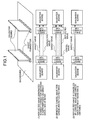
- FIG. 1 is a diagram for explaining an overview of an embodiment of the present invention
- FIG. 2 is a diagram for explaining a situation in which reflected waves are superimposed on a direct wave
- FIG. 3 is a diagram for explaining characteristics of an embodiment the present invention.
- FIG. 4 is a diagram of a constitution of a reflected wave cancellation circuit
- FIG. 5 is a functional block diagram of a constitution of a reflected wave cancellation circuit between daughter boards connected via a backboard;
- FIG. 6 is a functional block diagram of a constitution of a received waveform monitoring unit
- FIG. 7 is a diagram of a schematic constitution of counters
- FIGS. 8 to 10 are functional block diagrams of various example of a modification of the constitution of the received waveform monitoring unit
- FIGS. 11 to 15 are functional block diagrams of various modification of the constitution of the reflected wave cancellation circuit between the daughter boards connected via the backboard;
- FIG. 16 is a diagram for explaining a cancellation method for a complex reflected wave.
- FIG. 17 is a functional block diagram of a cancellation circuit for the complex reflected wave.
- backboard transmission in the present invention transmits a digital signal according to serial communication.
- the backboard transmission may supply electric power.
- a backboard transmission method of monitoring characteristics of reflected waves in a substrate unit on a reception side and canceling the reflected waves based on a result of the monitoring is described.
- various modifications of the backboard transmission method or the like of monitoring characteristics of reflected waves in a substrate unit on a reception side and canceling the reflected waves based on a result of the monitoring are described.
- FIG. 1 is a diagram for explaining an overview of the backboard transmission method according to the present invention.
- two daughter boards (substrate units) are inserted in sheet connectors (connectors) of a backboard (Back Wired Board (BWB)) to be perpendicular to the backboard.
- the daughter boards are mounted with integrated circuits like LSIs. In this way, the two daughter boards are connected as electric circuits via the backboard.
- BWB Back Wired Board
- the two daughter boards are connected to the backboard.
- two or more daughter boards are connected to the backboard.
- the illustration is simplified in this way to explain cancellation of reflected waves generated in communication between the two daughter boards.
- a direct wave of a signal transmitted from a transmission-side daughter board is reflected on a sheet connector of a reception-side daughter board to generate a reflected wave.
- the reflected wave is generated because backboard impedance of a circuit that forms a channel on the backboard does not match impedance of the sheet connector.
- impedance matching it is possible to perform impedance matching by reducing a distance between the output pin and the sheet connector and interposing a buffer in the section to prevent the generation of the reflected wave.
- the reflected wave is propagated backward on the channel of the direct wave and is further reflected on the sheet connector of the transmission-side daughter board to generate a further reflected wave.
- the reflected wave is superimposed on the direct wave to form noise that breaks a waveform of the direct wave (( 1 ) in FIG. 1 ).
- a cancellation wave having a characteristic capable of canceling a second reflected wave is generated and superimposed on a direct wave on which a reflected wave is superimposed (( 2 ) in FIG. 1 ).
- the reflected wave is canceled by the cancellation wave and a direct wave without noise mix is obtained (( 3 ) in FIG. 1 ).
- the present invention is characterized in that the reflected wave is removed from the direct wave in this way.
- FIG. 2 is a diagram for explaining a situation in which reflected waves are superimposed on a direct wave. It is assumed that two sheet connectors on a transmission side and a reception side shown in the figure have an identical characteristic.
- a pulse wave A(n,t) represented by a function of n (a bit number) and t (time) is transmitted from the transmission-side daughter board as a communication signal.
- R reflectance of a pulse wave on a sheet connector
- a direct received wave that reaches the reception side sheet connector as a direct wave is represented by Equation 1. (1 ⁇ R ) ⁇ A ( n,t ) (1)
- a reflected wave reflected on the sheet connector of the reception-side daughter board travels backward on the channel between the transmission-side daughter board and the reception-side daughter board and is further reflected on the sheet connector of the transmission-side daughter board.
- Time from the reflection on the sheet connector of the reception-side daughter board to the reflection on the sheet connector of the transmission-side daughter board is T.
- a gain of this reflected wave is lost because of the reflection on the sheet connector on the reception side.
- the first reflected wave is represented by Equation 2. (1 ⁇ R ) ⁇ R 2 ⁇ A ( n,t ⁇ T ) (2)
- One transmitted wave I 1 is directly inputted to a differential amplifier circuit.
- the other transmitted wave I 1 is subjected to waveform delay processing first.
- the waveform delay processing is processing for delaying respective terms of I 1 by T. Consequently, a transmitted wave I 2 subjected to the waveform delay processing is represented by Equation (6).
- Reflected wave extraction processing is applied to the transmitted wave I 2 .
- a reflection component I 3 of the transmitted wave I 2 is calculated by multiplying I 2 by R 2 .
- a transmitted wave I 3 subjected to the reflected wave extraction processing is represented by Equation (7).
- the transmitted wave I 3 is inputted to the differential amplifier circuit, subjected to output inversion, and superimposed on the transmitted wave I 1 separately inputted.
- I 4 (1 ⁇ R 1 ) ⁇ A ( n,t ) (8)
- FIG. 4 is a diagram of the constitution of the reflected wave cancellation circuit.
- a reflected wave cancellation circuit U includes a received-waveform monitoring unit 100 , a delay adjusting unit 150 , a gain adjusting unit 160 , a branch buffer 200 , and a differential amplification unit 300 .
- the reflected wave cancellation circuit U is formed over the transmission-side daughter board, the back board, the reception-side daughter board. In a conceptual constitution, any component may be mounted on any board.
- the branch buffer 200 is a buffer that branches an output wave from the integrated circuit of the transmission-side daughter board inputted into two.
- the branch buffer 200 also carries out a role of an amplifier that increases a gain of the output waves branched.
- the branched two output waves have an identical characteristic.
- One branched output, that is, a first branched output is inputted to the differential amplification unit 300 and the other branched output, that is, a second branched output, is inputted to the received-waveform monitoring unit 100 and the delay adjusting unit 150 .
- the received-waveform monitoring unit 100 detects a delay time T of a delay wave superimposed on the second branched output wave and reflectance R indicating a degree of attenuation of a gain.
- the delay time T and the reflectance R are inputted to the delay adjusting unit 150 and the gain adjusting unit 160 , respectively.
- the delay adjusting unit 150 receives the input of the delay time T and performs delay adjustment for the second branched output wave.
- the gain adjusting unit 160 receives the reflectance R and performs gain adjustment for the second branched output wave.
- the differential amplification unit 300 receives the input of the first branched output wave and the second branched output wave subjected to the gain adjustment by the gain adjusting unit 160 .
- the differential amplification unit 300 superimposes the second branched output wave subjected to output inversion on the first branched output wave to obtain an output wave with a reflected wave component cancelled.
- FIG. 5 is a functional block diagram of a constitution of a reflected wave cancellation circuit between daughter boards connected via a backboard.
- the reflected wave cancellation circuit U includes a transmission-side daughter board 500 that has a transmission side integrated circuit 510 and the branch buffer 200 , a backboard 600 that has sheet connectors 610 a and 610 b , and a reception-side daughter board 700 that has the received-waveform monitoring unit 100 , the delay adjusting unit 150 , the gain adjusting unit 160 , the differential amplification unit 300 , and a reception side integrated circuit 710 .
- the transmission side integrated circuit 510 is an electronic component that has a large number of signal output terminals such as an LSI. A digital signal carried by a serial wave is outputted from the signal output terminals. A signal wave outputted from the signal output terminals of the transmission side integrated circuit 510 is inputted to the branch buffer 200 and branched into a first branched output wave and a second branched output wave that have an identical characteristic. The first and the second branched output waves pass through a wiring circuit of the backboard 600 from the sheet connector 610 a to be inputted to the reception-side daughter board 700 from the sheet connector 610 b , respectively.
- the first branched output wave inputted to the reception-side daughter board 700 is directly inputted to the differential amplification unit 300 .
- the second branched output wave inputted to the reception-side daughter board 700 is inputted to the received-waveform monitoring unit 100 and the delay adjusting unit 150 .
- the delay adjusting unit 150 which receives the input of the delay time T from the received-waveform monitoring unit 100 , performs delay adjustment for the second branched output wave.
- the gain adjusting unit 160 which receives the input of the reflectance R from the received-waveform monitoring unit 100 , performs gain adjustment for the second branched output wave subjected to the delay adjustment by the delay adjusting unit 150 .
- the differential amplification unit 300 receives the input of the first branched output and the second branched output wave subjected to the gain adjustment by the gain adjusting unit 160 and extracts a direct wave with a reflected wave component cancelled.
- the direct wave with the reflected wave component cancelled is received by the reception side integrated circuit 710 and predetermined digital information is accurately passed.
- FIG. 6 is a functional block diagram of the constitution of the received-waveform monitoring unit shown in FIGS. 4 and 5 .
- the received-waveform monitoring unit 100 includes a signal input unit 101 , amplifiers 102 a and 102 b , an address counter 103 a , a counter 103 b , a comparator 104 , a DELAY or logic gate 105 , a peak hold circuit 106 , an AD converter 107 , memories 108 a and 108 b , a delay time output unit 109 a , and an amplitude-peak output unit 109 b.
- An input signal inputted to the signal input unit 101 is branched into a first input signal and a second input signal.
- the first input signal is used for detecting a delay time and the second input signal is used for detecting an amplitude (gain) peak for calculating a gain attenuation ratio.
- a gain of the first input signal is amplified by the amplifier 102 a and a gain of the second input signal is amplified by the amplifier 102 b.
- the first input signal with the gain amplified by the amplifier 102 a is branched into a signal inputted to the address counter 103 a , a signal directly inputted to the memory 108 a , a signal inputted to the comparator 104 , and a signal inputted to the DELAY or logic gate 105 .
- the address counter 103 a which receives the signal from the amplifier 102 a , increments a memory address and passes a memory address (A) counted at detection timing of a rising edge of the signal to the memories 108 a and 108 b .
- the comparator 104 clears the counter 103 b at arrival timing of a maximum amplitude pulse that arrives first after the counter 103 b is cleared last.
- the counter 103 b increments a memory address and passes a memory address (B) counted at clear timing of the counter 103 b to the memory 108 a .
- the delay time output unit 109 a calculates a delay time T of a reflected wave from the memory addresses (A) and (B) and passes the delay time T to the delay adjusting unit 150 .
- the DELAY or logic gate 105 inputs a delay wave of the first input signal to the peak hold circuit 106 and detects maximum amplitude of the reflected wave from comparison with the second input signal inputted.
- the AD converter 107 subjects information on this maximum amplitude to digital conversion and passes the information to the memory 108 b .
- the amplitude-peak output unit 109 b calculates reflectance (an attenuation ratio) by calculating a ratio of a maximum amplitude peak of the delay wave to a maximum amplitude peak of a direct wave and passes the reflectance to the gain adjusting unit 160 .
- the amplifiers 102 a and 102 b are provided to improve monitoring accuracy for the reflected wave. When the monitoring accuracy is sufficient, the amplifiers 102 a and 102 b do not have to be provided.
- FIG. 7 is a diagram of a schematic constitution of the address counter 103 a and the counter 103 b shown in FIG. 6 .
- the address counter 103 a and the counter 103 b include an oscillator 120 with a period 8 T, a phase delay unit 121 b for delay of time T, a phase delay unit 121 c for delay of time 2 T, a phase delay unit 121 d for delay of time 3 T, a phase delay unit 121 e for delay of time 4 T, a phase delay unit 121 f for delay of time 5 T, a phase delay unit 121 g for delay of time 6 T, a phase delay unit 121 h for delay of time 7 T, a first counter 122 a , a second counter 122 b , a third counter 122 c , a fourth counter 122 d , a fifth counter 122 e , a
- the first to the eighth counters 122 a to 122 h are identical 1-bit counters and operate at a period 8 T.
- the first counter 122 a is directly connected to the oscillator 120 and operates at an original period of the oscillator 120 .
- the second counter 122 b is connected to the oscillator 120 via the phase delay unit 121 b and operates at a period delayed by T from the original period of the oscillator 120 .
- the third counter 122 c is connected to the oscillator 120 via the phase delay unit 121 c and operates at a period delayed by 2 T from the original period of the oscillator 120 .
- the fourth counter 122 d is connected to the oscillator 120 via the phase delay unit 121 d and operates at a period delayed by 3 T from the original period of the oscillator 120 .
- the fifth counter 122 e is connected to the oscillator 120 via the phase delay unit 121 e and operates at a period delayed by 4 T from the original period of the oscillator 120 .
- the sixth counter 122 f is connected to the oscillator 120 via the phase delay unit 121 f and operates at a period delayed by 5 T from the original period of the oscillator 120 .
- the seventh counter 122 g is connected to the oscillator 120 via the phase delay unit 121 g and operates at a period delayed by 6 T from the original period of the oscillator 120 .
- the eighth counter 122 h is connected to the oscillator 120 via the phase delay unit 121 h and operates at a period delayed by 7 T from the original period of the oscillator 120 .
- the decode circuit 123 decodes counter count bits inputted from the first to the eight counters 122 a to 122 h . Input lines for clear signals are connected to the respective counters.
- a clock at which the counters are operable is branched and phases of the counters are delayed to operate the respective counters. This makes it possible to detect a delay time of a reflected wave superimposed on an output wave of a bit rate higher than that at the time when a 1-bit counter is independently used.
- the first embodiment of the present invention has been explained. However, the present invention is not limited to the first embodiment. The present invention may be further carried out in various different embodiments within the scope of the technical idea described in claims. In a second embodiment of the present invention, modifications of the first embodiment are described.
- FIGS. 8 to 10 are functional block diagrams of examples of a modification of the constitution of the received-waveform monitoring unit 100 shown in FIG. 6 .
- a pseudo-impedance 110 is provided between the signal input unit 101 and the amplifiers 102 a and 102 b of the received-waveform monitoring unit 100 in FIG. 6 . It is possible to change an input signal inputted to the signal input unit 101 to a periodic single pulse signal (a sample pulse) transmitted as a sample from a pulse generator separate from the transmission side integrated circuit by providing the pseudo-impedance 110 . When a characteristic of a delay wave is detected using the sample pulse periodically transmitted, it is possible to promptly cope with a change in impedance affected by an environmental change such as a temperature change.
- a NOT gate 111 to which a branched signal branched from the amplifier 102 a of the received-waveform monitoring unit 100 in FIG. 6 is inputted is added.
- a rising-edge-position delay-time output unit 109 a - 1 calculates a delay time T 1 at a rising edge of a pulse in.
- the NOT gate 111 inverts an input signal and passes the inverted signal to the address counter 103 c and the memory 109 c.
- the address counter 103 c can detect a rising edge of a pulse. Since the input signal is the inverted signal, the address counter 103 c detects a falling edge of the pulse of the signal before inversion by detecting the rising edge of the pulse. The address counter 103 c passes information on timing of the rising edge of the pulse to the memory 108 c . Information on the arrival timing of the maximum amplitude pulse is also passed to the memory 108 c from the counter 103 b .
- a falling-edge-position delay-time output unit 109 a - 2 calculates a delay time T 2 at the falling edge of the pulse from the information on the timing of the rising edge of the pulse, the information on the arrival timing of the maximum amplitude pulse, and an input wave directly inputted from the NOT gate 111 .
- Both the delay time T 1 at the rising edge of the pulse and the delay time T 2 at the falling edge of the pulse are inputted to the delay adjusting unit 150 .
- the delay adjusting unit 150 adopts an average of T 1 and T 2 as a delay time of the pulse.
- the pseudo-impedance 110 is provided between the signal input unit 101 and the amplifiers 102 a and 102 b of the received-waveform monitoring unit 100 in FIG. 9 .
- the purpose of adopting this constitution is as explained concerning the received-waveform monitoring unit 100 in FIG. 8 .
- FIGS. 11 to 15 are functional block diagrams of modifications of the constitution of the reflected wave cancellation circuit U between the daughter boards connected via the backboard shown in FIG. 5 .
- the delay adjusting unit 150 and the gain adjusting unit 160 are arranged on the transmission-side daughter board 500 .
- a delay-information output unit 130 a and a gain-information output unit 130 b are provided on the reception-side daughter board 700 and a delay-information detecting unit 140 a and a gain-information detecting unit 140 b are provided on the transmission-side daughter board 500 .
- Delay information of the reflected wave outputted by the received-waveform monitoring unit 100 is passed from the delay-information output unit 130 a to the delay-information detecting unit 140 a through the sheet connector 610 b , the backboard 600 , and the sheet connector 610 a and, then, inputted to the delay adjusting unit 150 .
- Gain information concerning the reflectance of the reflected wave outputted by the received-waveform monitoring unit 100 is passed from the gain-information output unit 130 b to the gain-information detecting unit 140 b through the sheet connector 610 b , the backboard 600 , and the sheet connector 610 a and, then, inputted to the gain adjusting unit 160 .
- the transmission side integrated circuit 510 has a signal output terminal D and a inverted signal output terminal xD.
- a cancellation wave for a reflected wave is generated using a inverted signal outputted from the inverted signal output terminal xD.
- the inverted signal outputted from the inverted signal output terminal xD is passed through a NOT gate 141 to be further inverted.
- the inverted signal coincides with a signal outputted from the signal output terminal D.
- a result of monitoring a waveform of this signal with the received-waveform monitoring unit 100 is used by the delay adjusting unit 150 and the gain adjusting unit 160 to cancel the reflected wave.
- the transmission side integrated circuit 510 further includes the delay adjusting unit 150 . It is possible to further reduce the size of the reflected wave cancellation circuit by using the transmission side integrated circuit 510 that includes the inverted signal output terminal xD and the delay adjusting unit 150 .
- the reception-side daughter board 700 includes the branch buffer 200 .
- the branch buffer 200 may be provided on the reception-side daughter board 700 or the transmission-side daughter board 500 .
- one channel may be shared in both transmission directions or different channels may be used in the respective transmission directions.
- the transmission-side daughter board 500 includes a single pulse generating unit 530 .
- the single pulse generating unit 530 periodically or singly generates a sample pulse that has a characteristic identical with a signal wave generated by the transmission side integrated circuit 510 .
- the single pulse generated by the pulse generating unit 530 is inputted to a branch buffer 200 b through the sheet connector 610 a , the backboard 600 , and the sheet connector 610 b .
- the signal wave generated by the transmission side integrated circuit 510 is inputted to a branch buffer 200 a through the sheet connector 610 a , the backboard 600 , and the sheet connector 610 b .
- the branch buffer 200 a and the branch buffer 200 b have identical impedance.
- the single pulse has to be passed through a branch buffer having impedance identical with that of a branch buffer for the signal wave generated by the transmission side integrated circuit 510 such that the single pulse has conditions identical with those of the signal wave.
- the received-waveform monitoring unit 100 of the reflected wave cancellation circuit U shown in FIG. 15 adopts the constitution shown in FIG. 8 or 11 .
- FIG. 16 is a diagram for explaining the cancellation method for the complex reflected wave.
- the complex reflected wave is generated by superimposing a plurality of reflected waves having different delay times and reflectances one on top of another. Since the superimposition is a linear addition, it is possible to sequentially cancel the respective reflected waves by forming different reflected wave cancellation circuits in the multi-stage constitution.
- the transmitted waves I 11 are represented by Equation (9).
- One transmitted wave I 11 is directly inputted to a differential amplifier circuit.
- the other transmitted wave I 11 is subjected to waveform delay processing first.
- the waveform delay processing is processing for delaying respective terms of I 11 by T 2 . Consequently, a transmitted wave I 12 subjected to the waveform delay processing is represented by Equation (10).
- the transmitted wave I 12 is subjected to reflected wave extraction processing.
- a reflection component I 13 of the transmitted wave I 12 is calculated by multiplying the transmitted wave I 12 by reflectance R 2 2 . Consequently, a transmitted wave I 13 subjected to the reflected wave extraction processing is represented by Equation (11).
- the transmitted wave I 13 is inputted to the differential amplifier circuit, subjected to output inversion, and superimposed on the transmitted wave I 11 separately inputted. In other words, by calculating I 11 -I 13 , it is possible to extract a transmitted wave I 14 with reflected waves having the delay time T 2 and the reflectance R 2 cancelled.
- the transmitted wave I 14 is represented by Equation (12).
- the transmitted wave I 14 is inputted to a branch buffer and the transmitted waves I 14 with reflected waves with the delay time T 1 and reflectance R 1 superimposed thereon is branched in two directions.
- One transmitted wave I 14 is directly inputted to a differential amplifier circuit.
- the other transmitted wave I 14 is subjected to waveform delay processing first.
- the waveform delay processing is processing for delaying respective terms of I 14 by T 1 . Consequently, a transmitted wave I 15 subjected to the waveform delay processing is represented by Equation (13).
- the transmitted wave I 15 is subjected to reflected wave extraction processing.
- a reflection component I 16 of the transmitted wave I 15 is calculated by multiplying the transmitted wave I 15 by reflectance R 1 2 . Consequently, a transmitted wave I 16 subjected to the reflected wave extraction processing is represented by Equation (14).
- the transmitted wave I 16 is inputted to the differential amplifier circuit, subjected to output inversion, and superimposed on the transmitted wave I 14 separately inputted.
- I 14 -I 16 it is possible to extract a signal wave I 17 with reflected waves having the delay time T 1 and the reflectance R 1 cancelled.
- FIG. 17 is a functional block diagram of the multi-stage cancellation circuit that realizes the cancellation method for a complex reflected wave shown in FIG. 16 .
- each of cancellation circuits U 1 to U n one output of the branch buffer 200 included in the cancellation circuit is connected to an input switching unit 800 .
- the input switching unit 800 selectively passes a branch signal from any one of the cancellation circuits U 1 to U n to the received-waveform monitoring unit 100 .
- the cancellation circuit, from which the branch signal is passed to the received-waveform monitoring unit 100 closes and operates.
- the received-waveform monitoring unit 100 passes a delay time and reflectance, which a result of received waveform monitoring, to the delay adjusting unit 150 and the gain adjusting unit 160 of each of the cancellation circuits U 1 to U n . It is possible to form a plurality of cancellation circuits in the multi-stage constitution in a small size by connecting the cancellation circuits U 1 to U n in parallel to the received-waveform monitoring unit 100 using the input switching unit 800 in this way.
- the reflected wave cancellation method and the reflected wave cancellation circuit of the present invention have been explained in the first and the second embodiments. It is possible to use both error correction and code conversion for a signal exchanged between the transmission-side daughter board 500 and the reception-side daughter board 700 . In particular, it is effective to use the error correction to further reduce an influence due to arrival of a reflected wave when a single pulse is transmitted.
- the functional block is divided into the transmission-side daughter board 500 and the reception-side daughter board 700 .
- both the functions on the transmission side and the reception side are mounted on one daughter board.
- the present invention is also possible to apply the present invention to removal of an influence of a reflected wave in a channel including a plurality of branches like an electric power line network.
- the present invention is applicable when there is an influence of a reflected wave in a channel for carrying electricity like electric power and electric signals.
- the transmission between the substrate units via the backboard it is possible to cancel reflected waves generated in the connector sections that connect the backboard and the substrate units. This makes it possible to prevent an influence of the reflected waves in high-speed communication of such transmission and secure and improve reliability of the communication.
- the signal wave for cancellation wave generation is the sample pulse periodically generated and transmitted from the transmission-side substrate unit. This makes it possible to quickly grasp characteristics of the reflected waves, which change according to a change in a surrounding environment, and accurately cancel the reflected waves.
Landscapes
- Engineering & Computer Science (AREA)
- Power Engineering (AREA)
- Computer Networks & Wireless Communication (AREA)
- Signal Processing (AREA)
- Dc Digital Transmission (AREA)
- Cable Transmission Systems, Equalization Of Radio And Reduction Of Echo (AREA)
Abstract
Description
(1−R)×A(n,t) (1)
(1−R)×R 2 ×A(n,t−T) (2)
(1−R)×R 2i ×A(n,t−iT) (3)
I 4=(1−R 1)×A(n,t) (8)
I 17=(1−R 1)×(1−R 2)×A(n,t) (15)
Claims (27)
Applications Claiming Priority (2)
| Application Number | Priority Date | Filing Date | Title |
|---|---|---|---|
| JP2006037222A JP4972948B2 (en) | 2006-02-14 | 2006-02-14 | Backboard transmission method, backboard transmission apparatus, and board unit |
| JP2006-037222 | 2006-02-14 |
Publications (2)
| Publication Number | Publication Date |
|---|---|
| US20070192051A1 US20070192051A1 (en) | 2007-08-16 |
| US7974799B2 true US7974799B2 (en) | 2011-07-05 |
Family
ID=38369778
Family Applications (1)
| Application Number | Title | Priority Date | Filing Date |
|---|---|---|---|
| US11/438,349 Expired - Fee Related US7974799B2 (en) | 2006-02-14 | 2006-05-23 | Backboard transmission method, backboard transmission apparatus, and substrate unit |
Country Status (2)
| Country | Link |
|---|---|
| US (1) | US7974799B2 (en) |
| JP (1) | JP4972948B2 (en) |
Cited By (2)
| Publication number | Priority date | Publication date | Assignee | Title |
|---|---|---|---|---|
| US20110316557A1 (en) * | 2009-01-28 | 2011-12-29 | Advantest Corporation | Test apparatus and test method |
| US8737492B1 (en) * | 2011-07-13 | 2014-05-27 | Netlogic Microsystems, Inc. | Methods, systems and circuits for cancelling reflections on a channel |
Families Citing this family (3)
| Publication number | Priority date | Publication date | Assignee | Title |
|---|---|---|---|---|
| CN102918815B (en) * | 2011-05-30 | 2016-03-30 | 华为技术有限公司 | Advanced telecom computing architecture data exchange system and power board, method for interchanging data |
| JP5772398B2 (en) * | 2011-08-30 | 2015-09-02 | 富士通株式会社 | Electronic component and reflected wave canceling method |
| US10528515B2 (en) | 2017-06-27 | 2020-01-07 | Intel Corporation | Memory channel driver with echo cancellation |
Citations (14)
| Publication number | Priority date | Publication date | Assignee | Title |
|---|---|---|---|---|
| JPS561634A (en) | 1979-06-20 | 1981-01-09 | Nec Corp | Equalizer |
| JPS61242174A (en) | 1985-04-19 | 1986-10-28 | Matsushita Electric Ind Co Ltd | Waveform equalizer |
| US20030038659A1 (en) * | 2001-05-24 | 2003-02-27 | Nec Corporation | Clock control circuit |
| US20030123649A1 (en) * | 2002-01-02 | 2003-07-03 | Casper Bryan K. | Echo cancellation using a variable offset comparator |
| US6628779B1 (en) * | 1998-05-11 | 2003-09-30 | Telcordia Technologies, Inc. | Method and system for scaleable near-end speech cancellation for tip and ring tone signal detectors |
| US20040001450A1 (en) * | 2002-06-24 | 2004-01-01 | He Perry P. | Monitoring and control of an adaptive filter in a communication system |
| US6693883B2 (en) * | 1997-10-22 | 2004-02-17 | Matsushita Electric Industrial Co., Ltd. | TDMA radio terminal capable of adjusting transmit timing by using measured delay time |
| US20040120391A1 (en) * | 2002-12-24 | 2004-06-24 | Chia-Liang Lin | Residual echo reduction for a full duplex transceiver |
| JP2004281960A (en) | 2003-03-19 | 2004-10-07 | Renesas Technology Corp | Ultra-high speed interface using intersymbol interference suppression resistor |
| US20040213170A1 (en) * | 2003-04-22 | 2004-10-28 | Gordon Bremer | Extended-performance echo-canceled duplex (EP ECD) communication |
| US20040246032A1 (en) * | 2003-03-03 | 2004-12-09 | Hiroyuki Ogiso | Clock shaping device and electronic instrument using the same |
| US20050052941A1 (en) * | 2002-06-25 | 2005-03-10 | Fujitsu Limited | Semiconductor memory |
| US20050100083A1 (en) * | 2003-10-16 | 2005-05-12 | Hiroshi Takatori | Full duplex transmission method |
| US20050152488A1 (en) * | 2003-12-16 | 2005-07-14 | California Institute Of Technology | Deterministic jitter equalizer |
Family Cites Families (4)
| Publication number | Priority date | Publication date | Assignee | Title |
|---|---|---|---|---|
| JPS5961234A (en) * | 1982-09-30 | 1984-04-07 | Nec Corp | Adaptive type echo erasing device |
| JP2001127614A (en) * | 1999-10-29 | 2001-05-11 | Nec Corp | Semiconductor integrated circuit and its impedance control method |
| JP2004242224A (en) * | 2003-02-10 | 2004-08-26 | Fujitsu Access Ltd | Reflected wave signal removal apparatus |
| JP4472274B2 (en) * | 2003-06-04 | 2010-06-02 | 株式会社ルネサステクノロジ | Signal transmission system and integrated circuit used therefor |
-
2006
- 2006-02-14 JP JP2006037222A patent/JP4972948B2/en not_active Expired - Fee Related
- 2006-05-23 US US11/438,349 patent/US7974799B2/en not_active Expired - Fee Related
Patent Citations (14)
| Publication number | Priority date | Publication date | Assignee | Title |
|---|---|---|---|---|
| JPS561634A (en) | 1979-06-20 | 1981-01-09 | Nec Corp | Equalizer |
| JPS61242174A (en) | 1985-04-19 | 1986-10-28 | Matsushita Electric Ind Co Ltd | Waveform equalizer |
| US6693883B2 (en) * | 1997-10-22 | 2004-02-17 | Matsushita Electric Industrial Co., Ltd. | TDMA radio terminal capable of adjusting transmit timing by using measured delay time |
| US6628779B1 (en) * | 1998-05-11 | 2003-09-30 | Telcordia Technologies, Inc. | Method and system for scaleable near-end speech cancellation for tip and ring tone signal detectors |
| US20030038659A1 (en) * | 2001-05-24 | 2003-02-27 | Nec Corporation | Clock control circuit |
| US20030123649A1 (en) * | 2002-01-02 | 2003-07-03 | Casper Bryan K. | Echo cancellation using a variable offset comparator |
| US20040001450A1 (en) * | 2002-06-24 | 2004-01-01 | He Perry P. | Monitoring and control of an adaptive filter in a communication system |
| US20050052941A1 (en) * | 2002-06-25 | 2005-03-10 | Fujitsu Limited | Semiconductor memory |
| US20040120391A1 (en) * | 2002-12-24 | 2004-06-24 | Chia-Liang Lin | Residual echo reduction for a full duplex transceiver |
| US20040246032A1 (en) * | 2003-03-03 | 2004-12-09 | Hiroyuki Ogiso | Clock shaping device and electronic instrument using the same |
| JP2004281960A (en) | 2003-03-19 | 2004-10-07 | Renesas Technology Corp | Ultra-high speed interface using intersymbol interference suppression resistor |
| US20040213170A1 (en) * | 2003-04-22 | 2004-10-28 | Gordon Bremer | Extended-performance echo-canceled duplex (EP ECD) communication |
| US20050100083A1 (en) * | 2003-10-16 | 2005-05-12 | Hiroshi Takatori | Full duplex transmission method |
| US20050152488A1 (en) * | 2003-12-16 | 2005-07-14 | California Institute Of Technology | Deterministic jitter equalizer |
Non-Patent Citations (1)
| Title |
|---|
| "Catalog of OMG IDL/Language Mappings Specification" [online] Mitsubishi Denki Kabushiki Kaisha https://www.mitsubishielectric.co.jp/news-data/2003/pdf/1002-b.pdf (submitted as "Potential Reduction in Size and Cost for Communication Network Repeater Units and Mobile Phone Base Station Units" (Fig. 1(a) and Fig. 1(b)). |
Cited By (2)
| Publication number | Priority date | Publication date | Assignee | Title |
|---|---|---|---|---|
| US20110316557A1 (en) * | 2009-01-28 | 2011-12-29 | Advantest Corporation | Test apparatus and test method |
| US8737492B1 (en) * | 2011-07-13 | 2014-05-27 | Netlogic Microsystems, Inc. | Methods, systems and circuits for cancelling reflections on a channel |
Also Published As
| Publication number | Publication date |
|---|---|
| JP2007221267A (en) | 2007-08-30 |
| US20070192051A1 (en) | 2007-08-16 |
| JP4972948B2 (en) | 2012-07-11 |
Similar Documents
| Publication | Publication Date | Title |
|---|---|---|
| US7974799B2 (en) | Backboard transmission method, backboard transmission apparatus, and substrate unit | |
| US9847865B2 (en) | System and method for digital cancellation of self-interference in full-duplex communications | |
| US7447260B2 (en) | Equalizer, equalization method, and transmitter | |
| JP4990123B2 (en) | Output buffer circuit and transmission method | |
| US20070289772A1 (en) | Electronic Circuit | |
| JPH0218658A (en) | Data processor | |
| US7786751B2 (en) | Differential signaling system and method of controlling skew between signal lines thereof | |
| JP2005244479A (en) | Transmission apparatus | |
| JP2017028489A (en) | Skew correction circuit, electronic device and skew correction method | |
| JP5057585B2 (en) | Method and apparatus for analog validation of high-speed bus using electromagnetic coupler | |
| KR100959846B1 (en) | Differential signal transmitter, differential signal receiver | |
| JP2001111408A (en) | High-speed signal transmission wiring mounting structure | |
| JP4236913B2 (en) | Data transfer device | |
| US8737450B2 (en) | High speed serial link systems | |
| JP4472274B2 (en) | Signal transmission system and integrated circuit used therefor | |
| CN111614355A (en) | Data transmission devices, analog-to-digital converters and radar systems | |
| WO2006017830A2 (en) | Line-doubler delay circuit | |
| JP6419402B1 (en) | Communication system and signal repeater | |
| US20030058803A1 (en) | Crosstalk equalization for input-output driver circuits | |
| US20140043097A1 (en) | Electronic device and noise reducing method | |
| KR100667180B1 (en) | Signal transfer device for easy noise rejection of transmitted signals | |
| CN115328849B (en) | Chip combined structure for data transmission and reception | |
| KR102023433B1 (en) | intermodulation canceling device and its method | |
| JP2008252374A (en) | Circuit board | |
| JPH117349A (en) | Electronic circuit and integrated circuit for noise reduction of bus wiring |
Legal Events
| Date | Code | Title | Description |
|---|---|---|---|
| AS | Assignment |
Owner name: FUJITSU LIMITED, JAPAN Free format text: ASSIGNMENT OF ASSIGNORS INTEREST;ASSIGNOR:IZUMI, FUTOSHI;REEL/FRAME:017917/0461 Effective date: 20060428 |
|
| STCF | Information on status: patent grant |
Free format text: PATENTED CASE |
|
| FEPP | Fee payment procedure |
Free format text: PAYER NUMBER DE-ASSIGNED (ORIGINAL EVENT CODE: RMPN); ENTITY STATUS OF PATENT OWNER: LARGE ENTITY Free format text: PAYOR NUMBER ASSIGNED (ORIGINAL EVENT CODE: ASPN); ENTITY STATUS OF PATENT OWNER: LARGE ENTITY |
|
| FPAY | Fee payment |
Year of fee payment: 4 |
|
| MAFP | Maintenance fee payment |
Free format text: PAYMENT OF MAINTENANCE FEE, 8TH YEAR, LARGE ENTITY (ORIGINAL EVENT CODE: M1552); ENTITY STATUS OF PATENT OWNER: LARGE ENTITY Year of fee payment: 8 |
|
| FEPP | Fee payment procedure |
Free format text: MAINTENANCE FEE REMINDER MAILED (ORIGINAL EVENT CODE: REM.); ENTITY STATUS OF PATENT OWNER: LARGE ENTITY |
|
| LAPS | Lapse for failure to pay maintenance fees |
Free format text: PATENT EXPIRED FOR FAILURE TO PAY MAINTENANCE FEES (ORIGINAL EVENT CODE: EXP.); ENTITY STATUS OF PATENT OWNER: LARGE ENTITY |
|
| STCH | Information on status: patent discontinuation |
Free format text: PATENT EXPIRED DUE TO NONPAYMENT OF MAINTENANCE FEES UNDER 37 CFR 1.362 |
|
| FP | Lapsed due to failure to pay maintenance fee |
Effective date: 20230705 |