US7855394B2 - LED array package covered with a highly thermal conductive plate - Google Patents
LED array package covered with a highly thermal conductive plate Download PDFInfo
- Publication number
- US7855394B2 US7855394B2 US12/487,453 US48745309A US7855394B2 US 7855394 B2 US7855394 B2 US 7855394B2 US 48745309 A US48745309 A US 48745309A US 7855394 B2 US7855394 B2 US 7855394B2
- Authority
- US
- United States
- Prior art keywords
- plate
- light source
- substrate
- emitting diode
- phosphor layer
- Prior art date
- Legal status (The legal status is an assumption and is not a legal conclusion. Google has not performed a legal analysis and makes no representation as to the accuracy of the status listed.)
- Active
Links
Images


Classifications
-
- H—ELECTRICITY
- H10—SEMICONDUCTOR DEVICES; ELECTRIC SOLID-STATE DEVICES NOT OTHERWISE PROVIDED FOR
- H10H—INORGANIC LIGHT-EMITTING SEMICONDUCTOR DEVICES HAVING POTENTIAL BARRIERS
- H10H20/00—Individual inorganic light-emitting semiconductor devices having potential barriers, e.g. light-emitting diodes [LED]
- H10H20/80—Constructional details
- H10H20/85—Packages
-
- F—MECHANICAL ENGINEERING; LIGHTING; HEATING; WEAPONS; BLASTING
- F21—LIGHTING
- F21K—NON-ELECTRIC LIGHT SOURCES USING LUMINESCENCE; LIGHT SOURCES USING ELECTROCHEMILUMINESCENCE; LIGHT SOURCES USING CHARGES OF COMBUSTIBLE MATERIAL; LIGHT SOURCES USING SEMICONDUCTOR DEVICES AS LIGHT-GENERATING ELEMENTS; LIGHT SOURCES NOT OTHERWISE PROVIDED FOR
- F21K9/00—Light sources using semiconductor devices as light-generating elements, e.g. using light-emitting diodes [LED] or lasers
- F21K9/60—Optical arrangements integrated in the light source, e.g. for improving the colour rendering index or the light extraction
- F21K9/64—Optical arrangements integrated in the light source, e.g. for improving the colour rendering index or the light extraction using wavelength conversion means distinct or spaced from the light-generating element, e.g. a remote phosphor layer
-
- F—MECHANICAL ENGINEERING; LIGHTING; HEATING; WEAPONS; BLASTING
- F21—LIGHTING
- F21V—FUNCTIONAL FEATURES OR DETAILS OF LIGHTING DEVICES OR SYSTEMS THEREOF; STRUCTURAL COMBINATIONS OF LIGHTING DEVICES WITH OTHER ARTICLES, NOT OTHERWISE PROVIDED FOR
- F21V29/00—Protecting lighting devices from thermal damage; Cooling or heating arrangements specially adapted for lighting devices or systems
- F21V29/50—Cooling arrangements
- F21V29/502—Cooling arrangements characterised by the adaptation for cooling of specific components
- F21V29/506—Cooling arrangements characterised by the adaptation for cooling of specific components of globes, bowls or cover glasses
-
- F—MECHANICAL ENGINEERING; LIGHTING; HEATING; WEAPONS; BLASTING
- F21—LIGHTING
- F21V—FUNCTIONAL FEATURES OR DETAILS OF LIGHTING DEVICES OR SYSTEMS THEREOF; STRUCTURAL COMBINATIONS OF LIGHTING DEVICES WITH OTHER ARTICLES, NOT OTHERWISE PROVIDED FOR
- F21V29/00—Protecting lighting devices from thermal damage; Cooling or heating arrangements specially adapted for lighting devices or systems
- F21V29/50—Cooling arrangements
- F21V29/70—Cooling arrangements characterised by passive heat-dissipating elements, e.g. heat-sinks
- F21V29/83—Cooling arrangements characterised by passive heat-dissipating elements, e.g. heat-sinks the elements having apertures, ducts or channels, e.g. heat radiation holes
-
- F—MECHANICAL ENGINEERING; LIGHTING; HEATING; WEAPONS; BLASTING
- F21—LIGHTING
- F21V—FUNCTIONAL FEATURES OR DETAILS OF LIGHTING DEVICES OR SYSTEMS THEREOF; STRUCTURAL COMBINATIONS OF LIGHTING DEVICES WITH OTHER ARTICLES, NOT OTHERWISE PROVIDED FOR
- F21V29/00—Protecting lighting devices from thermal damage; Cooling or heating arrangements specially adapted for lighting devices or systems
- F21V29/85—Protecting lighting devices from thermal damage; Cooling or heating arrangements specially adapted for lighting devices or systems characterised by the material
-
- H—ELECTRICITY
- H10—SEMICONDUCTOR DEVICES; ELECTRIC SOLID-STATE DEVICES NOT OTHERWISE PROVIDED FOR
- H10H—INORGANIC LIGHT-EMITTING SEMICONDUCTOR DEVICES HAVING POTENTIAL BARRIERS
- H10H20/00—Individual inorganic light-emitting semiconductor devices having potential barriers, e.g. light-emitting diodes [LED]
- H10H20/80—Constructional details
- H10H20/85—Packages
- H10H20/851—Wavelength conversion means
- H10H20/8515—Wavelength conversion means not being in contact with the bodies
-
- H—ELECTRICITY
- H10—SEMICONDUCTOR DEVICES; ELECTRIC SOLID-STATE DEVICES NOT OTHERWISE PROVIDED FOR
- H10H—INORGANIC LIGHT-EMITTING SEMICONDUCTOR DEVICES HAVING POTENTIAL BARRIERS
- H10H20/00—Individual inorganic light-emitting semiconductor devices having potential barriers, e.g. light-emitting diodes [LED]
- H10H20/80—Constructional details
- H10H20/85—Packages
- H10H20/858—Means for heat extraction or cooling
- H10H20/8583—Means for heat extraction or cooling not being in contact with the bodies
-
- H—ELECTRICITY
- H10—SEMICONDUCTOR DEVICES; ELECTRIC SOLID-STATE DEVICES NOT OTHERWISE PROVIDED FOR
- H10W—GENERIC PACKAGES, INTERCONNECTIONS, CONNECTORS OR OTHER CONSTRUCTIONAL DETAILS OF DEVICES COVERED BY CLASS H10
- H10W90/00—Package configurations
Definitions
- the present disclosure relates to a light emitting diode (LED) array package and, more particularly, to an LED array package with a highly thermal conductive plate.
- LED light emitting diode
- LEDs have been developed for many years and have been widely used in various light applications. As LEDs are light-weight, consume less energy, and have a good electrical power to light conversion efficiency, they have been used to replace conventional light sources, such as incandescent lamps and fluorescent light sources. LEDs may be utilized in an array package. For LED array packages, the temperature of a top surface of the package can reach 200° C. or more, which can damage the device. As such, there is a need in the art to improve the heat dissipation performance of LED array packages.
- a light source includes a substrate, a light emitting diode on the substrate, and a phosphor layer over the light emitting diode.
- a plate is on the phosphor layer.
- An attachment member is coupled to the plate and is configured to conduct heat away from the plate.
- a light source in another aspect of the disclosure, includes a substrate, a light emitting diode on the substrate, and a phosphor layer over the light emitting diode.
- the light source further includes first means for conducting heat away from the phosphor layer and second means for securing the first means to the light source and for conducting heat away from the first means.
- FIG. 1 is a cross-section view of a first example of an LED array package according to a first configuration.
- FIG. 2 is a cross-section view of a second example of an LED array package.
- FIG. 3 is a cross-section view of a third example of an LED array package.
- FIG. 4 is a cross-section view of a fourth example of an LED array package.
- FIG. 5 is a cross-section view of a fifth example of an LED array package.
- FIG. 6 is a cross-section view of a sixth example of an LED array package.
- FIG. 7 is a cross-section view of an LED array package according to a second configuration.
- FIG. 8 is a cross-section view of an LED array package according to a third configuration.
- FIG. 9 is a cross-section view of an LED array package according to a fourth configuration.
- FIG. 10 is a perspective view of the conductive glass plate.
- FIG. 11 is a top view of the LED array package of FIG. 7 .
- FIG. 12 is a top view of an LED array package according to a fifth configuration.
- FIG. 13 is a cross-sectional view of an LED array package according to a sixth configuration.
- FIG. 14 is a cross-sectional view of an LED array package according to a seventh configuration.
- FIG. 15 is a cross-sectional view of an LED array package according to an eighth configuration.
- relative terms such as “lower” or “bottom” and “upper” or “top,” may be used herein to describe one element's relationship to another element as illustrated in the drawings. It will be understood that relative terms are intended to encompass different orientations of an apparatus in addition to the orientation depicted in the drawings.
- the term “lower” can therefore encompass both an orientation of “lower” and “upper,” depending of the particular orientation of the apparatus.
- elements described as “below” or “beneath” other elements would then be oriented “above” the other elements.
- the terms “below” or “beneath” can therefore encompass both an orientation of above and below.
- an LED array package may be illustrated with reference to one or more exemplary configurations.
- the term “exemplary” means “serving as an example, instance, or illustration,” and should not necessarily be construed as preferred or advantageous over other configurations of an LED array package disclosed herein.
- FIG. 1 is a cross-section view of a first example of an LED array package 10 according to a first configuration.
- An LED is a semiconductor material impregnated, or doped, with impurities. These impurities add “electrons” and “holes” to the semiconductor, which can move in the material relatively freely.
- a doped region of the semiconductor can have predominantly electrons or holes, which is referred to as n-type or a p-type semiconductor region, respectively.
- the semiconductor includes an n-type semiconductor region and a p-type semiconductor region.
- a reverse electric field is created at the junction between the two regions, which cause the electrons and holes to move away from the junction to form an active region. When a forward voltage sufficient to overcome the reverse electric field is applied across the p-n junction, electrons and holes are forced into the active region and combine. When electrons combine with holes, they fall to lower energy levels and release energy in the form of light.
- the light source may be configured to produce white light.
- White light may enable the light source to act as a direct replacement for conventional light sources used today in incandescent and fluorescent light sources.
- One way is to use individual LEDs that emit red, green, and blue, and then mix all the colors to produce white light.
- the other way is to use a phosphor material to convert monochromatic light emitted from a blue or ultra-violet (UV) LED to broad-spectrum white light.
- UV ultra-violet
- the present invention may be practiced with other LED and phosphor combinations to produce different color lights.
- an array of LEDs 11 is on substrate 12 .
- the array of LEDs 11 may be covered with a layer 16 of a mixture of silicone and phosphor.
- U.S. patent application Ser. No. 12/164,506 entitled “A Light Emitting Device Having A Phosphor Layer” and which is herein incorporated by reference, provides several different additional configurations for the phosphor layer.
- a highly thermal conductive and transparent plate 13 is attached to a top surface of the LED array package 10 on the phosphor layer 16 .
- the plate 13 may be a sapphire plate, a silicone carbide (SiC) plate, a chemical-vapor-deposition (CVD) diamond plate, CVD SiC on a glass plate, CVD diamond on a glass plate, a glass plate, a zinc oxide (ZnO) plate, a quartz plate, or any of the aforementioned types of plates with a metal net (see FIG. 10 ).
- the plate 13 is secured to the phosphor layer by attachment member(s) 14 .
- the attachment member 14 includes a vertical member 14 a that extends between the substrate 12 and the plate 13 .
- the attachment member may further include a flange 14 b that fits over and secures the plate 13 .
- the attachment member 14 may be metal, such as aluminum, silver, copper, or another highly thermal conductive metal.
- the attachment member 14 may be in the shape of a ring and thermally bonded with the plate 13 .
- the attachment member 14 may surround the LED array package 10 and have an extrusion 14 c that extends parallel to the substrate 12 so that it can be thermally attached to the substrate 12 .
- the extrusion 14 c may include holes 14 c′ , which allow the LED array package 10 to be attached to a heat sink on a bottom surface of the substrate 12 through aligned holes 15 in the substrate 12 .
- the attachment member 14 may be secured to the substrate 12 with a thermal pad, epoxy, solder, or another adhesive, or may be secured with screws, bolts, or other fasteners through holes 14 c′ .
- the holes 14 c′ , 15 may be filled with thermal grease or paste, thus providing a good thermal dissipation path from the plate 13 , through the attachment member 14 , to an attached heat sink. While FIG. 1 shows an array of LEDs, the plate 13 and attachment member 14 may be utilized with any number of LEDs including just one LED.
- the temperature of a top surface of the LED array package 10 can reach 200° C. or more.
- the high temperature can significantly reduce the quantum efficiency of the phosphor or damage the whole device.
- the top surface of the LED array package can be significantly reduced with the highly thermal conductive plate 13 and an aluminum ring-shaped attachment member 14 , as shown in FIG. 1 .
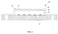
- FIG. 2 is a cross-section view of a second example of an LED array package 20 .
- the plate 13 and the attachment member 14 may be utilized with an LED array package 20 with a clear silicone layer 21 covering the LEDs 11 and a thin-film layer of phosphor 22 on the clear silicone layer 21 .
- FIG. 3 is a cross-section view of a third example of an LED array package 30 .
- the plate 13 and the attachment member 14 may be utilized with an LED array package 30 with a clear silicone layer 31 covering the LEDs 11 , a thin-film layer of phosphor 33 attached to a bottom surface of the plate 13 , and an intervening open air space 32 between the clear silicone layer 31 and the thin-film layer of phosphor 33 .
- FIG. 4 is a cross-section view of a fourth example of an LED array package 40 .
- the plate 13 and the attachment member 14 may be utilized with an LED array package 40 with a clear silicone dome layer 41 covering the LEDs 1 , a thin-film layer of phosphor 43 attached to the bottom surface of the plate 13 , and an intervening open air space 42 between the clear silicone dome layer 41 and the thin-film layer of phosphor 43 .
- the LEDs 11 may be blue LEDs.
- the clear silicone dome layer 41 extracts more blue light from the LED dies 11 , as less light is internally reflected at the interface of the air 42 and the clear silicone 41 .
- FIG. 5 is a cross-section view of a fifth example of an LED array package 50 .
- the plate 13 and the attachment member 14 may be utilized with an LED array package 50 with a clear silicone dome (or half-ball lens) array 51 covering the LEDs 1 , a thin-film layer of phosphor 53 attached to the bottom surface of the plate 13 , and an intervening open air space 52 between the clear silicone dome array 51 and the thin-film layer of phosphor 53 .
- the LEDs 11 may be blue LEDs.
- the clear silicone dome array 51 extracts more blue light from the LED dies 11 , as less light is internally reflected at the interface of the air 52 and the clear silicone 51 .
- FIG. 6 is a cross-section view of a sixth example of an LED array package 60 .
- the plate 13 and the attachment member 14 may be utilized with an LED array package 60 with a clear silicone layer 61 covering the LEDs 11 , a clear dome (or half-ball lens) array 62 bonded onto the clear silicone layer 61 , a thin-film layer of phosphor 64 attached to the bottom surface of the plate 13 , and an intervening open air space 63 between the clear silicone layer 61 and the thin-film layer of phosphor 64 .
- the clear dome array 62 may be silicone, preformed glass, or preformed plastic such as polymethylmethacrylate (PMMA), polycarbonate, acrylic, or another transparent material.
- the LEDs 11 may be blue LEDs.
- the clear dome array 62 extracts more blue light from the LED dies 11 , as less light is internally reflected at the interface of air 52 and the clear dome array 62 .
- FIG. 7 is a cross-section view of an LED array package 70 according to a second configuration.
- the attachment member 71 may not include the extrusions of the attachment member 14 .
- the attachment member 71 may be attached to the substrate 12 with an epoxy, solder, or another adhesive 72 attached between the substrate 12 and the attachment member 71 .
- FIG. 8 is a cross-section view of an LED array package 80 according to a third configuration.
- an array of LEDs 11 is on substrate 12 .
- a plate 13 may be attached to a top surface of the attachment member 81 .
- the plate 13 may be attached to the attachment member 81 with epoxy, solder, or another adhesive.
- the attachment member 81 includes a vertical member 81 a that extends between the substrate 12 and the plate 13 .
- the attachment member 81 may be metal, in the shape of a ring, and thermally bonded with the plate 13 .
- the attachment member 81 may surround the LED array package 80 and have an extrusion 81 b that extends parallel to the substrate 12 so that it can be thermally attached to the substrate 12 .
- the extrusion 81 b may include holes 81 b′ , which allow the LED array package 80 to be attached to a heat sink on a bottom surface of the substrate 12 through aligned holes 15 in the substrate 12 .
- the attachment member 81 may be secured to the substrate 12 with a thermal pad, epoxy, solder, or another adhesive, or may be secured with screws, bolts, or other fasteners through holes 81 b′ , 15 .
- the holes 81 b ′ may be filled with thermal grease or paste, thus providing a good thermal dissipation path from the plate 13 to an attached heat sink.
- FIG. 9 is a cross-section view of an LED array package 90 according to a fourth configuration.
- the attachment member 91 may not include the extrusions of the attachment member 81 .
- the attachment member 91 may be attached to the substrate 12 with an epoxy, solder, or another adhesive 92 attached between the substrate 12 and the attachment member 91 .
- FIG. 10 is a perspective view of the highly thermal conductive plate 13 .
- the plate 13 may include a metal net 100 on a top surface.
- the metal net 100 may be aluminum, copper, silver, or another highly thermally conductive metal.
- the metal net 100 may be on an outer surface of the plate 13 , as shown in FIG. 10 , or may be within the glass plate 13 .
- FIG. 11 is a top view of the LED array package 70 of FIG. 7 .
- the LED array package 70 includes a 5 ⁇ 5 array of LEDs 11 on substrate 12 .
- the ring-shaped attachment member 71 surrounds the LED array to secure the plate 13 (transparent in FIG. 11 ) on a top surface of the LED array and to conduct heat away from the plate 13 . Holes 15 allow the LED array package 70 to be secured to a heat sink.
- FIG. 11 shows the attachment member 71 in the shape of a ring, the attachment member 71 may be separate components and may not entirely surround the LED array. In an alternate configuration, two or more components may be utilized to secure the plate 13 to the LED array package 70 at specific points along the edge of the plate 13 .
- FIG. 12 is a top view of an LED array package 120 according to a fifth configuration.
- the LED array package 120 may include metal columns/walls 121 outside the LED array, and the plate 13 (transparent in FIG. 12 ) may be secured to the metal columns/walls 121 with epoxy, solder, or another adhesive.
- the configurations of a silicone layer, a phosphor layer, and any intervening open air space over the LEDs 11 applies also to the second through fifth configurations of the attachment member.
- the configurations can apply to any number of LEDs on a substrate, and therefore the configurations apply to a light emitting diode as well as to a light emitting diode array.
- a light source in one configuration, includes a substrate, a light emitting diode on the substrate, a phosphor over the light emitting diode, a first means for conducting heat away from the phosphor layer, and a second means for securing the first means to the light source and for conducting heat away from the first means.
- the first means is the plate 13 .
- the second means may be the attachment member 14 ( FIGS. 1-6 ), 71 ( FIGS. 7 , 11 ), 81 ( FIG. 8 ), or 91 ( FIG. 9 ) or may be the walls/columns 121 that extend vertically from the substrate as shown in FIG. 12 .
- FIGS. 13 , 14 , and 15 are cross-sectional views of LED array packages according to additional configurations.
- the plate 13 can be located between the phosphor layer 22 and the LEDs 11 .
- an additional plate 13 ′ may be located below the phosphor layer 22 , with the phosphor layer 22 sandwiched between the plate 13 and the plate 13 ′.
- the plate 13 and the phosphor layer 22 can be dome-shaped.
Landscapes
- Engineering & Computer Science (AREA)
- General Engineering & Computer Science (AREA)
- Physics & Mathematics (AREA)
- Microelectronics & Electronic Packaging (AREA)
- Optics & Photonics (AREA)
- Led Device Packages (AREA)
- Non-Portable Lighting Devices Or Systems Thereof (AREA)
Abstract
Description
Claims (18)
Priority Applications (8)
| Application Number | Priority Date | Filing Date | Title |
|---|---|---|---|
| US12/487,453 US7855394B2 (en) | 2009-06-18 | 2009-06-18 | LED array package covered with a highly thermal conductive plate |
| KR1020127000867A KR101295971B1 (en) | 2009-06-18 | 2010-05-30 | An led array package covered with a highly thermal conductive plate |
| EP10789925.4A EP2614528B1 (en) | 2009-06-18 | 2010-05-30 | An led array package covered with a highly thermal conductive plate |
| PCT/US2010/036783 WO2010147753A1 (en) | 2009-06-18 | 2010-05-30 | An led array package covered with a highly thermal conductive plate |
| CN201080035065.XA CN102484118B (en) | 2009-06-18 | 2010-05-30 | Adopt the LED array encapsulation that high thermal conductivity plate covers |
| JP2012516104A JP5469243B2 (en) | 2009-06-18 | 2010-05-30 | Light source with light emitting diode |
| TW099118870A TWI446600B (en) | 2009-06-18 | 2010-06-10 | LED array package with high-performance heat-conducting plate |
| US12/958,303 US8227828B2 (en) | 2009-06-18 | 2010-12-01 | LED array package covered with a highly thermal conductive plate |
Applications Claiming Priority (1)
| Application Number | Priority Date | Filing Date | Title |
|---|---|---|---|
| US12/487,453 US7855394B2 (en) | 2009-06-18 | 2009-06-18 | LED array package covered with a highly thermal conductive plate |
Related Child Applications (1)
| Application Number | Title | Priority Date | Filing Date |
|---|---|---|---|
| US12/958,303 Continuation US8227828B2 (en) | 2009-06-18 | 2010-12-01 | LED array package covered with a highly thermal conductive plate |
Publications (2)
| Publication Number | Publication Date |
|---|---|
| US20100133556A1 US20100133556A1 (en) | 2010-06-03 |
| US7855394B2 true US7855394B2 (en) | 2010-12-21 |
Family
ID=42221960
Family Applications (2)
| Application Number | Title | Priority Date | Filing Date |
|---|---|---|---|
| US12/487,453 Active US7855394B2 (en) | 2009-06-18 | 2009-06-18 | LED array package covered with a highly thermal conductive plate |
| US12/958,303 Active US8227828B2 (en) | 2009-06-18 | 2010-12-01 | LED array package covered with a highly thermal conductive plate |
Family Applications After (1)
| Application Number | Title | Priority Date | Filing Date |
|---|---|---|---|
| US12/958,303 Active US8227828B2 (en) | 2009-06-18 | 2010-12-01 | LED array package covered with a highly thermal conductive plate |
Country Status (7)
| Country | Link |
|---|---|
| US (2) | US7855394B2 (en) |
| EP (1) | EP2614528B1 (en) |
| JP (1) | JP5469243B2 (en) |
| KR (1) | KR101295971B1 (en) |
| CN (1) | CN102484118B (en) |
| TW (1) | TWI446600B (en) |
| WO (1) | WO2010147753A1 (en) |
Cited By (2)
| Publication number | Priority date | Publication date | Assignee | Title |
|---|---|---|---|---|
| US20110220162A1 (en) * | 2010-03-15 | 2011-09-15 | Siivola Edward P | Thermoelectric (TE) Devices/Structures Including Thermoelectric Elements with Exposed Major Surfaces |
| US20230232658A1 (en) * | 2022-01-17 | 2023-07-20 | Samsung Display Co., Ltd. | Display device and method for manufacturing the same |
Families Citing this family (40)
| Publication number | Priority date | Publication date | Assignee | Title |
|---|---|---|---|---|
| US10008637B2 (en) | 2011-12-06 | 2018-06-26 | Cree, Inc. | Light emitter devices and methods with reduced dimensions and improved light output |
| US9151468B2 (en) * | 2010-06-28 | 2015-10-06 | Axlen, Inc. | High brightness illumination devices using wavelength conversion materials |
| US20120012865A1 (en) * | 2010-07-19 | 2012-01-19 | Jianhua Li | Led array package with a high thermally conductive plate |
| JP5733743B2 (en) * | 2010-12-15 | 2015-06-10 | 日東電工株式会社 | Optical semiconductor device |
| DE102011017633A1 (en) * | 2011-04-27 | 2012-10-31 | Osram Ag | A method of forming a phosphor array and associated phosphor array |
| KR101212654B1 (en) * | 2011-05-20 | 2012-12-14 | (주)라이타이저코리아 | Package for light emitting diode and method for manufacturing thereof |
| KR101262541B1 (en) | 2011-07-18 | 2013-05-08 | 엘지이노텍 주식회사 | Display device |
| KR101823684B1 (en) * | 2011-07-18 | 2018-01-30 | 엘지이노텍 주식회사 | Display device |
| US10211380B2 (en) | 2011-07-21 | 2019-02-19 | Cree, Inc. | Light emitting devices and components having improved chemical resistance and related methods |
| KR20140038553A (en) | 2011-07-21 | 2014-03-28 | 크리,인코포레이티드 | Light emitter device packages, components, and mehtods for improved chemical resistance and related methods |
| US10686107B2 (en) | 2011-07-21 | 2020-06-16 | Cree, Inc. | Light emitter devices and components with improved chemical resistance and related methods |
| US9496466B2 (en) | 2011-12-06 | 2016-11-15 | Cree, Inc. | Light emitter devices and methods, utilizing light emitting diodes (LEDs), for improved light extraction |
| US8917010B2 (en) * | 2012-02-02 | 2014-12-23 | Citizen Electronics Co., Ltd. | Lighting device including phosphor layer and light-transmitting layer that is arranged in contact with the phosphor layer to release static charge to substrate |
| US9240530B2 (en) * | 2012-02-13 | 2016-01-19 | Cree, Inc. | Light emitter devices having improved chemical and physical resistance and related methods |
| US9343441B2 (en) | 2012-02-13 | 2016-05-17 | Cree, Inc. | Light emitter devices having improved light output and related methods |
| JP5936885B2 (en) * | 2012-03-05 | 2016-06-22 | シチズンホールディングス株式会社 | Semiconductor light emitting device |
| DE102012207854A1 (en) | 2012-05-11 | 2013-11-14 | Osram Opto Semiconductors Gmbh | OPTOELECTRONIC COMPONENT AND METHOD FOR MANUFACTURING AN OPTOELECTRONIC COMPONENT |
| JP2014022451A (en) * | 2012-07-13 | 2014-02-03 | Citizen Electronics Co Ltd | Phosphor lens sheet and production method therefor, and light-emitting device including phosphor lens sheet |
| CN103811642B (en) * | 2012-11-12 | 2016-06-22 | 厦门兴恒隆照明科技有限公司 | A kind of remote LED specular removal light-emitting phosphor thin film and LED light source |
| TWI499094B (en) * | 2013-01-25 | 2015-09-01 | Achrolux Inc | Led package and method for fabricating the same |
| US10002855B2 (en) | 2013-02-11 | 2018-06-19 | Lumileds Llc | LED module with hermetic seal of wavelength conversion material |
| US9324692B2 (en) * | 2013-02-18 | 2016-04-26 | Nthdegree Technologies Worldwide Inc. | Transparent LED layer between phosphor layer and light exit surface of lamp |
| JP6104682B2 (en) * | 2013-04-09 | 2017-03-29 | シチズン電子株式会社 | Lighting device |
| WO2014198619A1 (en) | 2013-06-14 | 2014-12-18 | Koninklijke Philips N.V. | Light emitting device |
| JP6053621B2 (en) * | 2013-06-21 | 2016-12-27 | シチズン時計株式会社 | Light emitting device |
| WO2015042193A2 (en) * | 2013-09-17 | 2015-03-26 | Xicato, Inc. | Led based illumination device with integrated output window |
| CN103840067A (en) * | 2013-12-31 | 2014-06-04 | 吴震 | Wavelength conversion device and light-emitting device |
| KR102323289B1 (en) * | 2014-01-07 | 2021-11-08 | 루미리즈 홀딩 비.브이. | Glueless light emitting device with phosphor converter |
| KR20150093283A (en) * | 2014-02-06 | 2015-08-18 | 삼성디스플레이 주식회사 | Frame and light source module comprising the same |
| WO2015138495A1 (en) * | 2014-03-11 | 2015-09-17 | Osram Sylvania Inc. | Light converter assemblies with enhanced heat dissipation |
| KR102166715B1 (en) | 2014-04-02 | 2020-10-19 | 삼성디스플레이 주식회사 | Light source unit, and method for manufacturing the same, and backlight assembly including the same |
| DE102014106164A1 (en) * | 2014-05-02 | 2015-11-05 | Itz Innovations- Und Technologiezentrum Gmbh | Thermally conductive optics |
| EP3146263B1 (en) * | 2014-05-21 | 2019-09-25 | Lumileds Holding B.V. | Method of attaching a lens to a led module with high alignment accuracy |
| US9541273B2 (en) * | 2014-05-22 | 2017-01-10 | Wen-Sung Hu | Heat dissipation structure of SMD LED |
| JP6448365B2 (en) * | 2014-12-26 | 2019-01-09 | シチズン時計株式会社 | Light emitting device and projection device |
| US9985182B2 (en) * | 2015-12-25 | 2018-05-29 | Citizen Electronics Co., Ltd. | Light-emitting apparatus and color-matching apparatus |
| WO2018002809A1 (en) * | 2016-06-29 | 2018-01-04 | Sabic Global Technologies B.V. | Fabrication of phosphor film with heat dissipation film |
| CN109728149B (en) * | 2017-10-30 | 2024-12-06 | 深圳市铭上光电有限公司 | Integrated infrared LED packaging structure resistant to external interference and preparation method thereof |
| EP3717830A4 (en) | 2017-11-27 | 2021-05-26 | Glint Photonics, Inc. | CONFIGURABLE LIGHTS AND COMPONENTS |
| CN109586165B (en) * | 2019-01-25 | 2020-04-07 | 维沃移动通信有限公司 | Laser module and electronic equipment |
Citations (6)
| Publication number | Priority date | Publication date | Assignee | Title |
|---|---|---|---|---|
| US20040113549A1 (en) | 2001-01-31 | 2004-06-17 | Roberts John K | High power radiation emitter device and heat dissipating package for electronic components |
| US20060290251A1 (en) | 2005-06-27 | 2006-12-28 | Shives Gary D | Display device having improved properties |
| US20070040097A1 (en) * | 2005-08-19 | 2007-02-22 | Mok Thye L | Electronic flash, imaging device and method for producing a flash of light having a rectangular radiation pattern |
| US20090296369A1 (en) * | 2008-05-30 | 2009-12-03 | Bridgelux, Inc. | Method and Apparatus for Generating White Light From Solid State Light Emitting Devices |
| US20090322197A1 (en) * | 2008-06-30 | 2009-12-31 | Rene Helbing | Light emitting device having a transparent thermally conductive layer |
| US20100065878A1 (en) * | 2004-02-02 | 2010-03-18 | 3M Innovative Properties Company | Adhesive sheet for light-emitting diode device and light-emitting diode device |
Family Cites Families (17)
| Publication number | Priority date | Publication date | Assignee | Title |
|---|---|---|---|---|
| US6639360B2 (en) * | 2001-01-31 | 2003-10-28 | Gentex Corporation | High power radiation emitter device and heat dissipating package for electronic components |
| US6812503B2 (en) * | 2001-11-29 | 2004-11-02 | Highlink Technology Corporation | Light-emitting device with improved reliability |
| JP2005005544A (en) * | 2003-06-13 | 2005-01-06 | Sumitomo Electric Ind Ltd | White light emitting device |
| US20070262702A1 (en) * | 2004-03-31 | 2007-11-15 | Shunsuke Fujita | Phoshor and Light-Emitting Diode |
| US9104058B2 (en) * | 2005-06-27 | 2015-08-11 | Graftech International Holdings Inc. | Optimized frame system for a liquid crystal display device |
| JP2007081234A (en) * | 2005-09-15 | 2007-03-29 | Toyoda Gosei Co Ltd | Lighting device |
| US7196354B1 (en) * | 2005-09-29 | 2007-03-27 | Luminus Devices, Inc. | Wavelength-converting light-emitting devices |
| EP1963743B1 (en) * | 2005-12-21 | 2016-09-07 | Cree, Inc. | Lighting device |
| KR100764391B1 (en) * | 2006-04-25 | 2007-10-05 | 삼성전기주식회사 | Light emitting diode module |
| JP5036332B2 (en) * | 2007-01-26 | 2012-09-26 | スタンレー電気株式会社 | Light emitting device and color conversion filter |
| JP4953846B2 (en) * | 2007-02-06 | 2012-06-13 | スタンレー電気株式会社 | Light emitting device and manufacturing method thereof |
| TW200847489A (en) * | 2007-02-27 | 2008-12-01 | Kyocera Corp | Light-emitting device |
| JP5480466B2 (en) * | 2007-06-26 | 2014-04-23 | パナソニック株式会社 | Light emitting device |
| US8076833B2 (en) * | 2008-06-30 | 2011-12-13 | Bridgelux, Inc. | Methods and apparatuses for enhancing heat dissipation from a light emitting device |
| US7851819B2 (en) * | 2009-02-26 | 2010-12-14 | Bridgelux, Inc. | Transparent heat spreader for LEDs |
| WO2010123052A1 (en) * | 2009-04-22 | 2010-10-28 | シーシーエス株式会社 | Light-emitting device |
| KR20110035190A (en) * | 2009-09-30 | 2011-04-06 | 엘지이노텍 주식회사 | Light emitting device |
-
2009
- 2009-06-18 US US12/487,453 patent/US7855394B2/en active Active
-
2010
- 2010-05-30 EP EP10789925.4A patent/EP2614528B1/en active Active
- 2010-05-30 WO PCT/US2010/036783 patent/WO2010147753A1/en not_active Ceased
- 2010-05-30 CN CN201080035065.XA patent/CN102484118B/en active Active
- 2010-05-30 KR KR1020127000867A patent/KR101295971B1/en active Active
- 2010-05-30 JP JP2012516104A patent/JP5469243B2/en active Active
- 2010-06-10 TW TW099118870A patent/TWI446600B/en active
- 2010-12-01 US US12/958,303 patent/US8227828B2/en active Active
Patent Citations (6)
| Publication number | Priority date | Publication date | Assignee | Title |
|---|---|---|---|---|
| US20040113549A1 (en) | 2001-01-31 | 2004-06-17 | Roberts John K | High power radiation emitter device and heat dissipating package for electronic components |
| US20100065878A1 (en) * | 2004-02-02 | 2010-03-18 | 3M Innovative Properties Company | Adhesive sheet for light-emitting diode device and light-emitting diode device |
| US20060290251A1 (en) | 2005-06-27 | 2006-12-28 | Shives Gary D | Display device having improved properties |
| US20070040097A1 (en) * | 2005-08-19 | 2007-02-22 | Mok Thye L | Electronic flash, imaging device and method for producing a flash of light having a rectangular radiation pattern |
| US20090296369A1 (en) * | 2008-05-30 | 2009-12-03 | Bridgelux, Inc. | Method and Apparatus for Generating White Light From Solid State Light Emitting Devices |
| US20090322197A1 (en) * | 2008-06-30 | 2009-12-31 | Rene Helbing | Light emitting device having a transparent thermally conductive layer |
Non-Patent Citations (1)
| Title |
|---|
| PCT/US2010/036783-Notification of transmitttal of the international search report and the written opinion of the international searching authority, or the declaration. Jul. 28, 2010. |
Cited By (2)
| Publication number | Priority date | Publication date | Assignee | Title |
|---|---|---|---|---|
| US20110220162A1 (en) * | 2010-03-15 | 2011-09-15 | Siivola Edward P | Thermoelectric (TE) Devices/Structures Including Thermoelectric Elements with Exposed Major Surfaces |
| US20230232658A1 (en) * | 2022-01-17 | 2023-07-20 | Samsung Display Co., Ltd. | Display device and method for manufacturing the same |
Also Published As
| Publication number | Publication date |
|---|---|
| EP2614528B1 (en) | 2016-12-07 |
| JP2012531040A (en) | 2012-12-06 |
| CN102484118B (en) | 2016-06-29 |
| TW201110432A (en) | 2011-03-16 |
| US20110073878A1 (en) | 2011-03-31 |
| WO2010147753A1 (en) | 2010-12-23 |
| JP5469243B2 (en) | 2014-04-16 |
| CN102484118A (en) | 2012-05-30 |
| EP2614528A4 (en) | 2013-12-11 |
| KR20120052227A (en) | 2012-05-23 |
| US20100133556A1 (en) | 2010-06-03 |
| TWI446600B (en) | 2014-07-21 |
| KR101295971B1 (en) | 2013-08-13 |
| US8227828B2 (en) | 2012-07-24 |
| EP2614528A1 (en) | 2013-07-17 |
Similar Documents
| Publication | Publication Date | Title |
|---|---|---|
| US7855394B2 (en) | LED array package covered with a highly thermal conductive plate | |
| US20240234387A9 (en) | Light-emitting device array with individual cells | |
| TWI614920B (en) | Optoelectronic device and method for manufacturing the same | |
| TWI425652B (en) | Solid state light emitting device and its manufacturing method | |
| US8076680B2 (en) | LED package having an array of light emitting cells coupled in series | |
| CN101142692B (en) | Light emitting diode package with array of light emitting cells coupled in series | |
| US20120012865A1 (en) | Led array package with a high thermally conductive plate | |
| CN103715188B (en) | LED emitter with improved white appearance | |
| WO2012015530A2 (en) | Phosphor layer having enhanced thermal conduction and light sources utilizing the phosphor layer | |
| CN102576783A (en) | Pixelated led | |
| US20120012864A1 (en) | Led array package with a color filter | |
| US8937324B2 (en) | Light-emitting device array with individual cells | |
| US20110063846A1 (en) | Extended source light module | |
| JP6062675B2 (en) | Light emitting device and lighting device | |
| HK1171286B (en) | An led array package covered with a highly thermal conductive plate | |
| HK1171286A (en) | An led array package covered with a highly thermal conductive plate | |
| KR20200143851A (en) | Semiconductor device package |
Legal Events
| Date | Code | Title | Description |
|---|---|---|---|
| AS | Assignment |
Owner name: BRIDGELUX, INC.,CALIFORNIA Free format text: ASSIGNMENT OF ASSIGNORS INTEREST;ASSIGNORS:LI, JIANHUA, MR.;HELBING, RENE;HUM, DAVID, MR.;REEL/FRAME:022847/0190 Effective date: 20090616 Owner name: BRIDGELUX, INC., CALIFORNIA Free format text: ASSIGNMENT OF ASSIGNORS INTEREST;ASSIGNORS:LI, JIANHUA, MR.;HELBING, RENE;HUM, DAVID, MR.;REEL/FRAME:022847/0190 Effective date: 20090616 |
|
| SULP | Surcharge for late payment | ||
| STCF | Information on status: patent grant |
Free format text: PATENTED CASE |
|
| AS | Assignment |
Owner name: WHITE OAK GLOBAL ADVISORS, LLC, AS COLLATERAL AGEN Free format text: SECURITY AGREEMENT;ASSIGNOR:BRIDGELUX, INC.;REEL/FRAME:029281/0844 Effective date: 20121109 |
|
| AS | Assignment |
Owner name: BRIDGELUX, INC., CALIFORNIA Free format text: TERMINATION AND RELEASE OF SECURITY INTEREST IN PATENT COLLATERAL RECORDED AT REEL/FRAME 029281/0844 ON NOVEMBER 12, 2012;ASSIGNOR:WELLS FARGO BANK, NATIONAL ASSOCIATION (SUCCESSOR BY ASSIGNMENT FROM WHITE OAK GLOBAL ADVISORS, LLC, AS COLLATERAL AGENT);REEL/FRAME:031560/0102 Effective date: 20131029 |
|
| FPAY | Fee payment |
Year of fee payment: 4 |
|
| MAFP | Maintenance fee payment |
Free format text: PAYMENT OF MAINTENANCE FEE, 8TH YEAR, LARGE ENTITY (ORIGINAL EVENT CODE: M1552) Year of fee payment: 8 |
|
| MAFP | Maintenance fee payment |
Free format text: PAYMENT OF MAINTENANCE FEE, 12TH YEAR, LARGE ENTITY (ORIGINAL EVENT CODE: M1553); ENTITY STATUS OF PATENT OWNER: LARGE ENTITY Year of fee payment: 12 |