US7820366B2 - Method of writing identifying information on wafer - Google Patents
Method of writing identifying information on wafer Download PDFInfo
- Publication number
- US7820366B2 US7820366B2 US11/350,733 US35073306A US7820366B2 US 7820366 B2 US7820366 B2 US 7820366B2 US 35073306 A US35073306 A US 35073306A US 7820366 B2 US7820366 B2 US 7820366B2
- Authority
- US
- United States
- Prior art keywords
- identifying information
- patterned
- film
- pattern
- resist layer
- Prior art date
- Legal status (The legal status is an assumption and is not a legal conclusion. Google has not performed a legal analysis and makes no representation as to the accuracy of the status listed.)
- Expired - Fee Related, expires
Links
- 238000000034 method Methods 0.000 title claims abstract description 67
- 238000005530 etching Methods 0.000 claims abstract description 13
- 239000010408 film Substances 0.000 claims description 133
- 239000010409 thin film Substances 0.000 claims description 32
- 230000000149 penetrating effect Effects 0.000 claims 4
- 229920002120 photoresistant polymer Polymers 0.000 claims 1
- 239000002184 metal Substances 0.000 abstract description 41
- 238000000206 photolithography Methods 0.000 description 20
- 239000000463 material Substances 0.000 description 5
- 238000004544 sputter deposition Methods 0.000 description 4
- 238000000992 sputter etching Methods 0.000 description 4
- 230000000694 effects Effects 0.000 description 3
- 238000001312 dry etching Methods 0.000 description 2
- 238000001020 plasma etching Methods 0.000 description 2
- 238000007747 plating Methods 0.000 description 2
- 239000004065 semiconductor Substances 0.000 description 2
- 239000007769 metal material Substances 0.000 description 1
- 238000012986 modification Methods 0.000 description 1
- 230000004048 modification Effects 0.000 description 1
- 238000000059 patterning Methods 0.000 description 1
- 230000002265 prevention Effects 0.000 description 1
- 238000004886 process control Methods 0.000 description 1
- 239000000758 substrate Substances 0.000 description 1
Images


Classifications
-
- G—PHYSICS
- G03—PHOTOGRAPHY; CINEMATOGRAPHY; ANALOGOUS TECHNIQUES USING WAVES OTHER THAN OPTICAL WAVES; ELECTROGRAPHY; HOLOGRAPHY
- G03F—PHOTOMECHANICAL PRODUCTION OF TEXTURED OR PATTERNED SURFACES, e.g. FOR PRINTING, FOR PROCESSING OF SEMICONDUCTOR DEVICES; MATERIALS THEREFOR; ORIGINALS THEREFOR; APPARATUS SPECIALLY ADAPTED THEREFOR
- G03F7/00—Photomechanical, e.g. photolithographic, production of textured or patterned surfaces, e.g. printing surfaces; Materials therefor, e.g. comprising photoresists; Apparatus specially adapted therefor
- G03F7/70—Microphotolithographic exposure; Apparatus therefor
- G03F7/70425—Imaging strategies, e.g. for increasing throughput or resolution, printing product fields larger than the image field or compensating lithography- or non-lithography errors, e.g. proximity correction, mix-and-match, stitching or double patterning
- G03F7/70466—Multiple exposures, e.g. combination of fine and coarse exposures, double patterning or multiple exposures for printing a single feature
-
- G—PHYSICS
- G03—PHOTOGRAPHY; CINEMATOGRAPHY; ANALOGOUS TECHNIQUES USING WAVES OTHER THAN OPTICAL WAVES; ELECTROGRAPHY; HOLOGRAPHY
- G03F—PHOTOMECHANICAL PRODUCTION OF TEXTURED OR PATTERNED SURFACES, e.g. FOR PRINTING, FOR PROCESSING OF SEMICONDUCTOR DEVICES; MATERIALS THEREFOR; ORIGINALS THEREFOR; APPARATUS SPECIALLY ADAPTED THEREFOR
- G03F7/00—Photomechanical, e.g. photolithographic, production of textured or patterned surfaces, e.g. printing surfaces; Materials therefor, e.g. comprising photoresists; Apparatus specially adapted therefor
- G03F7/70—Microphotolithographic exposure; Apparatus therefor
- G03F7/70483—Information management; Active and passive control; Testing; Wafer monitoring, e.g. pattern monitoring
- G03F7/70491—Information management, e.g. software; Active and passive control, e.g. details of controlling exposure processes or exposure tool monitoring processes
- G03F7/70541—Tagging, i.e. hardware or software tagging of features or components, e.g. using tagging scripts or tagging identifier codes for identification of chips, shots or wafers
-
- G—PHYSICS
- G03—PHOTOGRAPHY; CINEMATOGRAPHY; ANALOGOUS TECHNIQUES USING WAVES OTHER THAN OPTICAL WAVES; ELECTROGRAPHY; HOLOGRAPHY
- G03F—PHOTOMECHANICAL PRODUCTION OF TEXTURED OR PATTERNED SURFACES, e.g. FOR PRINTING, FOR PROCESSING OF SEMICONDUCTOR DEVICES; MATERIALS THEREFOR; ORIGINALS THEREFOR; APPARATUS SPECIALLY ADAPTED THEREFOR
- G03F9/00—Registration or positioning of originals, masks, frames, photographic sheets or textured or patterned surfaces, e.g. automatically
- G03F9/70—Registration or positioning of originals, masks, frames, photographic sheets or textured or patterned surfaces, e.g. automatically for microlithography
- G03F9/7073—Alignment marks and their environment
- G03F9/708—Mark formation
-
- G—PHYSICS
- G03—PHOTOGRAPHY; CINEMATOGRAPHY; ANALOGOUS TECHNIQUES USING WAVES OTHER THAN OPTICAL WAVES; ELECTROGRAPHY; HOLOGRAPHY
- G03F—PHOTOMECHANICAL PRODUCTION OF TEXTURED OR PATTERNED SURFACES, e.g. FOR PRINTING, FOR PROCESSING OF SEMICONDUCTOR DEVICES; MATERIALS THEREFOR; ORIGINALS THEREFOR; APPARATUS SPECIALLY ADAPTED THEREFOR
- G03F9/00—Registration or positioning of originals, masks, frames, photographic sheets or textured or patterned surfaces, e.g. automatically
- G03F9/70—Registration or positioning of originals, masks, frames, photographic sheets or textured or patterned surfaces, e.g. automatically for microlithography
- G03F9/7073—Alignment marks and their environment
- G03F9/7084—Position of mark on substrate, i.e. position in (x, y, z) of mark, e.g. buried or resist covered mark, mark on rearside, at the substrate edge, in the circuit area, latent image mark, marks in plural levels
-
- H—ELECTRICITY
- H01—ELECTRIC ELEMENTS
- H01L—SEMICONDUCTOR DEVICES NOT COVERED BY CLASS H10
- H01L23/00—Details of semiconductor or other solid state devices
- H01L23/544—Marks applied to semiconductor devices or parts, e.g. registration marks, alignment structures, wafer maps
-
- H—ELECTRICITY
- H01—ELECTRIC ELEMENTS
- H01L—SEMICONDUCTOR DEVICES NOT COVERED BY CLASS H10
- H01L2223/00—Details relating to semiconductor or other solid state devices covered by the group H01L23/00
- H01L2223/544—Marks applied to semiconductor devices or parts
- H01L2223/54406—Marks applied to semiconductor devices or parts comprising alphanumeric information
-
- H—ELECTRICITY
- H01—ELECTRIC ELEMENTS
- H01L—SEMICONDUCTOR DEVICES NOT COVERED BY CLASS H10
- H01L2223/00—Details relating to semiconductor or other solid state devices covered by the group H01L23/00
- H01L2223/544—Marks applied to semiconductor devices or parts
- H01L2223/54426—Marks applied to semiconductor devices or parts for alignment
-
- H—ELECTRICITY
- H01—ELECTRIC ELEMENTS
- H01L—SEMICONDUCTOR DEVICES NOT COVERED BY CLASS H10
- H01L2223/00—Details relating to semiconductor or other solid state devices covered by the group H01L23/00
- H01L2223/544—Marks applied to semiconductor devices or parts
- H01L2223/54433—Marks applied to semiconductor devices or parts containing identification or tracking information
-
- H—ELECTRICITY
- H01—ELECTRIC ELEMENTS
- H01L—SEMICONDUCTOR DEVICES NOT COVERED BY CLASS H10
- H01L2223/00—Details relating to semiconductor or other solid state devices covered by the group H01L23/00
- H01L2223/544—Marks applied to semiconductor devices or parts
- H01L2223/54473—Marks applied to semiconductor devices or parts for use after dicing
- H01L2223/5448—Located on chip prior to dicing and remaining on chip after dicing
-
- H—ELECTRICITY
- H01—ELECTRIC ELEMENTS
- H01L—SEMICONDUCTOR DEVICES NOT COVERED BY CLASS H10
- H01L2924/00—Indexing scheme for arrangements or methods for connecting or disconnecting semiconductor or solid-state bodies as covered by H01L24/00
- H01L2924/0001—Technical content checked by a classifier
- H01L2924/0002—Not covered by any one of groups H01L24/00, H01L24/00 and H01L2224/00
Definitions
- the present invention relates to a method of writing identifying information on a wafer, wherein the identifying information is written by photolithography on the wafer used for forming thin-film elements.
- Thin-film elements manufactured through thin-film forming techniques include those manufactured by forming a plurality of thin-film elements on a wafer (substrate) through the use of the thin-film forming techniques and then separating the wafer into the individual thin-film elements.
- Such thin-film elements include semiconductor elements and thin-film magnetic heads.
- the above-mentioned thin-film elements are manufactured through a plurality of steps.
- alignment marks are formed on the wafer for alignment performed in the following step.
- Such alignment marks may be made of patterned films that are patterned through the use of photolithography, for example.
- Japanese Published Patent Application 2002-184672 discloses a technique in which alignment marks for a batch exposure apparatus and alignment marks for a reducing exposure apparatus are formed on a wafer in a first photolithography step.
- wafer identifying information and element location identifying information are written on each of the above-mentioned thin-film elements for objectives such as process control and prevention of nonconforming products, wherein the wafer identifying information is used for identifying the wafer to which each of the thin-film elements belongs, and the element location identifying information is used for identifying the location of each of the thin-film elements on the wafer.
- These items of identification information are written on the wafer at a point before the wafer is divided into the respective thin-film elements.
- the identification information is also made of patterned films that are patterned through the use of photolithography, for example.
- Japanese Published Patent Application 62-20116 discloses a technique in which, on a wafer on which a plurality of thin-film magnetic heads are to be formed, marks for identifying the respective heads are formed in a batch by photolithography.
- identifying information is written on the wafer through the use of photolithography, using an alignment mark that is first formed (that may be hereinafter called the first alignment mark) as a reference indicating the location.
- This case may be one in which a patterned film for the first alignment mark and a patterned film for the identifying information are formed at the same heights by patterning a single thin film.
- the patterned film for the first alignment mark is formed, and then a photolithography step for forming the patterned film for the identifying information is performed using the patterned film for the first alignment mark as the reference of the location.
- FIG. 34 is a flowchart showing the related-art method of writing identifying information.
- FIG. 35A to FIG. 45A , FIG. 35B to FIG. 45B , FIG. 35C to FIG. 45C , and FIG. 35D to FIG. 45D are views for illustrating the steps of the method of writing identifying information of FIG. 34 .
- FIG. 45D each illustrate a state of a layered structure made up of a wafer and layers formed thereon.
- FIG. 35A to FIG. 45A each illustrate a top surface of a region in which the identifying information is to be located.
- FIG. 35B to FIG. 45B each illustrate a top surface of a region in which the first alignment mark is to be located.
- FIG. 35C to FIG. 45C each illustrate a cross section of the region in which the identifying information is to be located.
- FIG. 35D to FIG. 45D each illustrate a cross section of the region in which the first alignment mark is to be located.
- the region in which the identifying information is to be located may be a rectangular region, for example, surrounding the identifying information.
- the region in which the first alignment mark is to be located may be a rectangular region, for example, surrounding the first alignment mark.
- a metal film 212 is formed on the wafer 211 by sputtering, for example (step S 201 ).
- a resist layer 214 is formed by applying a resist to the top of the metal film 212 (step S 202 ).
- the resist used here may be positive one, for example.
- the resist layer 214 is exposed through masks 215 and 216 (step S 203 ).
- the mask 215 is formed to intercept light in an entire region where the identifying information is to be located.
- the mask 216 is designed so that, in the region where the first alignment mark is to be located, light is intercepted in portions corresponding to the pattern of the first alignment mark, and light is allowed to pass through in the other portions.
- the resist layer 214 is developed (step S 204 ). In the region where the identifying information is to be located, the resist layer 214 developed entirely remains. In the region where the first alignment mark is to be located, portions of the resist layer 214 developed that correspond to the pattern of the first alignment mark only remain.
- the steps surrounded by the broken line indicated with S 21 that is, the steps from S 202 to S 204 , are the photolithography steps for forming the first alignment mark.
- the metal film 212 is selectively etched, using the resist layer 214 as an etching mask (step S 205 ). As a result, in the region where the identifying information is to be located, the metal film 212 entirely remains. In the region where the first alignment mark is to be located, portions of the metal film 212 that correspond to the pattern of the first alignment mark only remain. The portions of the metal film 212 remaining in the region where the first alignment mark is to be located become a patterned film 212 A for the first alignment mark. Next, as shown in FIG. 40A to FIG. 40D , the resist layer 214 is removed (step S 206 ).
- a resist layer 217 is formed by applying a resist to the entire top surface of the layered structure (step S 207 ).
- the resist used here may be positive one, for example.
- the resist layer 217 is exposed through masks 218 and 219 (step S 208 ).
- the mask 218 is designed so that, in the region where the identifying information is to be located, light is intercepted in portions corresponding to the pattern of the identifying information, and light is allowed to pass through in the other portions.
- the mask 219 is formed to intercept light in the entire region where the first alignment mark is to be located. In this step, the masks 218 and 219 are aligned using the patterned film 212 A for the first alignment mark as the reference of the location.
- the resist layer 217 is developed (step S 209 ).
- steps of the resist layer 217 developed that correspond to the pattern of the identifying information only remain.
- the steps surrounded by the broken line indicated with S 22 that is, the steps from S 207 to S 209 , are the photolithography steps for writing the identifying information.
- the metal film 212 is selectively etched, using the resist layer 217 as an etching mask (step S 210 ). As a result, in the region where the identifying information is to be located, portions of the metal film 212 that correspond to the pattern of the identifying information only remain. These remaining portions of the metal film 212 become a patterned film 212 B for the identifying information. In the region where the first alignment mark is to be located, the patterned film 212 A remains as it is.
- the resist layer 217 is removed (step S 211 ), and the steps for writing the identifying information are thereby completed.
- FIG. 35A to FIG. 45A , FIG. 35B to FIG. 45B , FIG. 35C to FIG. 45C , and FIG. 35D to FIG. 45D there arises a problem that, since the method includes a great number of steps, a long period of time and costs are required for forming the patterned film for the first alignment mark and the patterned film for the identifying information.
- a method of writing identifying information on a wafer of the invention for writing identifying information through the use of a patterned resist layer on a wafer used for forming thin-film elements.
- the method comprises: the step of forming a resist layer on the wafer; the first exposure step of exposing the resist layer based on a first pattern for an alignment mark by projecting the first pattern onto the resist layer; the first development step of developing the resist layer to form a pattern to be a reference of a location in the resist layer, the first development step being performed after the first exposure step; the second exposure step of exposing the resist layer based on a second pattern for the identifying information by projecting the second pattern onto the resist layer, using the pattern formed in the resist layer in the first development step as the reference of the location; the second development step of developing the resist layer to form a patterned resist layer after the second exposure step; and the patterned film forming step of forming a patterned film for the alignment mark that is patterned based on the first pattern and a patterned film for the identifying information that
- the method of the invention may further comprise the step of forming a film to be etched that is located below the resist layer, the step being performed before the step of forming the resist layer, wherein, in the patterned film forming step, the film to be etched may be selectively etched, using the patterned resist layer as an etching mask, and the patterned film for the alignment mark and the patterned film for the identifying information may be thereby formed of remaining portions of the film etched.
- the patterned resist layer may have a groove, and, in the patterned film forming step, the patterned film for the alignment mark and the patterned film for the identifying information may be formed by forming a film in the groove of the patterned resist layer.
- development in the first development step, development may be performed such that a part of a portion of the resist layer soluble in a developer remains, the part being close to the wafer.
- a plurality of exposure regions may be predetermined on the wafer, and processing of projecting the first pattern onto the resist layer may be repeated for the respective exposure regions.
- processing of projecting the second pattern onto the resist layer may be repeated for the respective exposure regions.
- a plurality of element regions in each of which a thin-film element is to be formed may be predetermined in the exposure regions, and, in the second exposure step, exposure may be performed such that the second pattern is projected for each of the element regions.
- the identifying information may include wafer identifying information for identifying the wafer.
- the identifying information may include element location identifying information for identifying a location of each of the thin-film elements in the wafer.
- the resist layer is exposed based on the first pattern for the alignment mark.
- the resist layer is developed and the pattern to be the reference of the location is thereby formed in the resist layer.
- the resist layer is exposed based on the second pattern for the identifying information by projecting the second pattern onto the resist layer, using the pattern formed in the resist layer in the first development step as the reference of the location.
- FIG. 1 is view for illustrating a wafer to which a first embodiment of the invention is applied.
- FIG. 2 is a flowchart showing a method of writing identifying information of the first embodiment of the invention.
- FIG. 3A to FIG. 3D are views for illustrating a step of the method of writing identifying information of the first embodiment of the invention.
- FIG. 4A to FIG. 4D are views for illustrating a step that follows the step shown in FIG. 3A to FIG. 3D .
- FIG. 5A to FIG. 5D are views for illustrating a step that follows the step shown in FIG. 4A to FIG. 4D .
- FIG. 6A to FIG. 6D are views for illustrating a step that follows the step shown in FIG. 5A to FIG. 5D .
- FIG. 7A to FIG. 7D are views for illustrating a step that follows the step shown in FIG. 6A to FIG. 6D .
- FIG. 8A to FIG. 8D are views for illustrating a step that follows the step shown in FIG. 7A to FIG. 7D .
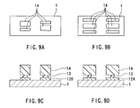
- FIG. 9A to FIG. 9D are views for illustrating a step that follows the step shown in FIG. 8A to FIG. 8D .
- FIG. 10A to FIG. 10D are views for illustrating a step that follows the step shown in FIG. 9A to FIG. 9D .
- FIG. 11A to FIG. 11D are views for illustrating a step of a method of writing identifying information of a second embodiment of the invention.
- FIG. 13A to FIG. 13D are views for illustrating a step that follows the step shown in FIG. 12A to FIG. 12D .
- FIG. 14A to FIG. 14D are views for illustrating a step that follows the step shown in FIG. 13A to FIG. 13D .
- FIG. 15A to FIG. 15D are views for illustrating a step that follows the step shown in FIG. 14A to FIG. 14D .
- FIG. 16A to FIG. 16D are views for illustrating a step that follows the step shown in FIG. 15A to FIG. 15D .
- FIG. 17 is a flowchart showing a method of writing identifying information of a third embodiment of the invention.
- FIG. 18A to FIG. 18D are views for illustrating a step of the method of writing identifying information of the third embodiment of the invention.
- FIG. 19A to FIG. 19D are views for illustrating a step that follows the step shown in FIG. 18A to FIG. 18D .
- FIG. 20A to FIG. 20D are views for illustrating a step that follows the step shown in FIG. 19A to FIG. 19D .
- FIG. 21A to FIG. 21D are views for illustrating a step that follows the step shown in FIG. 20A to FIG. 20D .
- FIG. 22A to FIG. 22D are views for illustrating a step that follows the step shown in FIG. 21A to FIG. 21D .
- FIG. 23A to FIG. 23D are views for illustrating a step that follows the step shown in FIG. 22A to FIG. 22D .
- FIG. 24A to FIG. 24D are views for illustrating a step that follows the step shown in FIG. 23A to FIG. 23D .
- FIG. 25 is a flowchart showing a method of writing identifying information of a fourth embodiment of the invention.
- FIG. 26A to FIG. 26D are views for illustrating a step of the method of writing identifying information of the fourth embodiment of the invention.
- FIG. 27A to FIG. 27D are views for illustrating a step that follows the step shown in FIG. 26A to FIG. 26D .
- FIG. 28A to FIG. 28D are views for illustrating a step that follows the step shown in FIG. 27A to FIG. 27D .
- FIG. 29A to FIG. 29D are views for illustrating a step that follows the step shown in FIG. 28A to FIG. 28D .
- FIG. 30A to FIG. 30D are views for illustrating a step that follows the step shown in FIG. 29A to FIG. 29D .
- FIG. 31A to FIG. 31D are views for illustrating a step that follows the step shown in FIG. 30A to FIG. 30D .
- FIG. 32A to FIG. 32D are views for illustrating a step that follows the step shown in FIG. 31A to FIG. 31D .
- FIG. 33A to FIG. 33D are views for illustrating a step that follows the step shown in FIG. 32A to FIG. 32D .
- FIG. 34 is a flowchart showing a method of writing identifying information of related art.
- FIG. 35A to FIG. 35D are views for illustrating a step of the method of writing identifying information of FIG. 34 .
- FIG. 36A to FIG. 36D are views for illustrating a step that follows the step shown in FIG. 35A to FIG. 35D .
- FIG. 37A to FIG. 37D are views for illustrating a step that follows the step shown in FIG. 36A to FIG. 36D .
- FIG. 38A to FIG. 38D are views for illustrating a step that follows the step shown in FIG. 37A to FIG. 37D .
- FIG. 39A to FIG. 39D are views for illustrating a step that follows the step shown in FIG. 38A to FIG. 38D .
- FIG. 40A to FIG. 40D are views for illustrating a step that follows the step shown in FIG. 39A to FIG. 39D .
- FIG. 41A to FIG. 41D are views for illustrating a step that follows the step shown in FIG. 40A to FIG. 40D .
- FIG. 42A to FIG. 42D are views for illustrating a step that follows the step shown in FIG. 41A to FIG. 41D .
- FIG. 43A to FIG. 43D are views for illustrating a step that follows the step shown in FIG. 42A to FIG. 42D .
- FIG. 44A to FIG. 44D are views for illustrating a step that follows the step shown in FIG. 43A to FIG. 43D .
- FIG. 45A to FIG. 45D are views for illustrating a step that follows the step shown in FIG. 44A to FIG. 44D .
- FIG. 1 is a view for illustrating the wafer to which the first embodiment is applied.
- a plurality of exposure regions 2 are predetermined on the wafer 1 to which the embodiment is applied.
- the exposure regions 2 are those in which a specific pattern is projected onto a resist layer described later by a single exposure processing.
- an alignment mark 3 that is first formed is located in each of the exposure regions 2 .
- a plurality of element regions 4 in which respective thin-film elements are formed are predetermined in each of the exposure regions 2 .
- the alignment mark 3 is located in a region of each of the exposure regions 2 that has an area equal to the area of several ones of the element regions 4 , for example.
- the thin-film elements may be semiconductor elements or microdevices such as thin-film magnetic heads.
- identifying information 5 is written in each of the element regions 4 .
- FIG. 1( d ) illustrates an example in which the identifying information 5 is written at two points in the element region 4
- the identifying information 5 may be written at one point in the element region 4 or three or more points in the element region 4 .
- the identifying information 5 includes wafer identifying information 5 A for identifying the wafer 1 , and element location identifying information 5 B for identifying the location of each of the thin-film elements on the wafer 1 .
- Each of the wafer identifying information 5 A and the element location identifying information 5 B includes a plurality of digits each of which is indicated with a numeral or an alphabet.
- the same wafer identifying information 5 A is allocated to each of the element regions 4 on the wafer 1 .
- different sorts of element location identifying information 5 B are allocated to the respective element regions 4 .
- FIG. 2 is a flowchart showing the method of writing the identifying information of the embodiment.
- FIG. 3A to FIG. 10A , FIG. 3B to FIG. 10B , FIG. 3C to FIG. 10C , and FIG. 3D to FIG. 10D are views for illustrating the steps of the method.
- FIG. 3A to FIG. 10A , FIG. 3B to FIG. 10B , FIG. 3C to FIG. 10C , and FIG. 3D to FIG. 10D are views for illustrating the steps of the method.
- FIG. 3A to FIG. 10A , FIG. 3B to FIG. 10B , FIG. 3C to FIG. 10C , and FIG. 3D to FIG. 10D are views for illustrating the steps of the method.
- FIG. 10A , FIG. 3B to FIG. 10B , FIG. 3C to FIG. 10C , and FIG. 3D to FIG. 10D each illustrate a state of a layered structure made up of the wafer 1 and layers formed thereon.
- FIG. 3A to FIG. 10A each illustrate a top surface of a region in which the identifying information 5 is to be located.
- FIG. 3B to FIG. 10B each illustrate a top surface of a region in which the alignment mark 3 is to be located.
- FIG. 3C to FIG. 10C each illustrate a cross section of the region in which the identifying information 5 is to be located.
- FIG. 3D to FIG. 10D each illustrate a cross section of the region in which the alignment mark 3 is to be located.
- the region in which the identifying information 5 is to be located may be a rectangular region, for example, surrounding the identifying information 5 .
- the region in which the alignment mark 3 is to be located may be a rectangular region, for example, surrounding the alignment mark 3 .
- a metal film 12 as a film to be etched is formed on the wafer 1 by sputtering, for example (step S 101 ).
- the metal film 12 may be made of any metal material that is not transparent, such as Ti.
- two resist layers 13 and 14 are formed by applying two kinds of resists to the top of the metal film 12 one by one (step S 102 ).
- the resist layer 13 is the lower one and the resist layer 14 is the upper one.
- the resists forming the resist layers 13 and 14 are positive ones, the resists may be negative ones.
- the lower resist layer 13 may be one that is not photosensitive as long as it is soluble in a developer.
- FIG. 4A to FIG. 4D show the example in which the two resist layers 13 and 14 are formed, a single resist layer may be formed by applying one kind of resist to the top of the metal film 12 .
- the resist layers 13 and 14 are exposed through masks 15 and 16 (step S 103 ).
- the mask 15 is formed to intercept light in an entire region where the identifying information 5 is to be located.
- the mask 16 has a first pattern for the alignment mark 3 . That is, the mask 16 is designed so that, in the region where the alignment mark 3 is to be located, light is intercepted in portions corresponding to the pattern of the alignment mark 3 , and light is allowed to pass through in the other portions.
- the first pattern for the alignment mark 3 is projected onto the resist layers 13 and 14 , and the resist layers 13 and 14 are thereby exposed based on the first pattern. This step is performed for each of the exposure regions 2 and repeated until exposure of all the exposure regions 2 is completed. This step corresponds to the first exposure step of the invention.
- step S 104 the resist layers 13 and 14 are developed to form a pattern to be a reference of a location.
- This step corresponds to the first development step of the invention.
- development is performed such that parts of portions of the resist layers 13 and 14 soluble in the developer remain, the parts being close to the wafer 1 . If the resists forming the resist layers 13 and 14 are positive, the portions to which light for exposure is applied become soluble in the developer. If the resists forming the resist layers 13 and 14 are negative, the portions to which light for exposure is not applied become soluble in the developer.
- FIG. 6A to FIG. 6D show an example in which development is performed such that the entire resist layer 13 touching the metal film 12 and a part of the resist layer 14 close to the wafer 1 remain.
- the resist layer 14 developed has: a convex portion 14 a located in the entire region where the identifying information 5 is to be located; a convex portion 14 b having a shape corresponding to the pattern of the alignment mark 3 and located in the region where the alignment mark 3 is to be located; and a lower portion 14 c other than the convex portions 14 a and 14 b .
- the top surface of the lower portion 14 c is located at a level lower than the top surfaces of the convex portions 14 a and 14 b (a level closer to the top surface of the wafer 1 ).
- This difference in level makes it possible to recognize the location and shape of the convex portion 14 b by observing the convex portion 14 b with a microscope, for example.
- the pattern of the convex portion 14 b is the one that serves as the reference of the location.
- the steps surrounded by the broken line indicated with S 11 that is, the steps from S 102 to S 104 , are the photolithography steps for forming the alignment mark 3 .
- the mask 17 has a second pattern for the identifying information 5 . That is, the mask 17 is designed so that, in the region where the identifying information 5 is to be located, light is intercepted in portions corresponding to the pattern of the identifying information 5 , and light is allowed to pass through in the other portions.
- the mask 18 is formed to intercept light in the entire region where the alignment mark 3 is to be located.
- the second pattern for the identifying information 5 is projected onto the resist layers 13 and 14 , and the resist layers 13 and 14 are thereby exposed based on the second pattern.
- the resist layers 13 and 14 are actually multi-exposed based on the pattern for the wafer identifying information 5 A and the pattern for the element location identifying information 5 B.
- This step is performed for each of the exposure regions 2 and repeated until exposure of all the exposure regions 2 is completed. In this step, exposure is performed such that the second pattern for the identifying information 5 is projected for each of the element regions 4 .
- This step corresponds to the second exposure step of the invention.
- Projection of the second pattern onto the resist layers 13 and 14 is performed using the pattern formed in the resist layer 14 in the development step of the step S 104 , that is, the pattern of the convex portion 14 b , as the reference of the location. That is, the masks 17 and 18 are aligned using the pattern formed in the resist layer 14 in the development step of the step S 104 , that is, the pattern of the convex portion 14 b , as the reference of the location.
- the convex portion 14 b has a shape corresponding to the pattern of the alignment mark 3 . Therefore, although the alignment mark 3 is not formed yet at this point, it is possible to align the masks 17 and 18 in a manner similar to the case in which alignment is performed using the alignment mark 3 as the reference of the location after the alignment mark 3 is formed.
- the resist layers 13 and 14 are developed to form the patterned resist layers 13 and 14 (step S 106 ).
- steps S 105 and S 106 are the photolithography steps for writing the identifying information 5 .
- the metal film 12 is selectively etched by ion milling, for example, using the resist layers 13 and 14 as etching masks (step S 107 ).
- steps S 107 the metal film 12 is selectively etched by ion milling, for example, using the resist layers 13 and 14 as etching masks.
- the patterned film 12 A for the alignment mark 3 and the patterned film 12 B for the identifying information 5 are formed through the use of the patterned resist layers 13 and 14 , wherein the patterned film 12 A is patterned based on the first pattern while the patterned film 12 B is patterned based on the second pattern.
- This step corresponds to the patterned film forming step of the invention.
- the patterned films 12 A and 12 B are formed at the same height, using the same metal film 12 .
- the method of etching the metal film 12 is not limited to ion milling but may be any sort of dry etching such as reactive ion etching.
- the resist layers 13 and 14 are removed (step S 108 ), and the steps for writing the identifying information 5 are thereby completed.
- the alignment mark 3 is used as the reference of the location in the photolithography steps performed after the alignment mark 3 is formed.
- the embodiment does not require the etching step of the step S 205 of FIG. 34 , the step of removing the resist layer of the step S 206 , and the step of applying resist of the step S 207 .
- FIG. 11A to FIG. 16A , FIG. 11B to FIG. 16B , FIG. 11C to FIG. 16C , and FIG. 11D to FIG. 16D are views for illustrating the steps of the method.
- FIG. 11A to FIG. 16A , FIG. 11B to FIG. 16B , FIG. 11C to FIG. 16C , and FIG. 11D to FIG. 16D are views for illustrating the steps of the method.
- FIG. 16D each illustrate a state of a layered structure made up of the wafer 1 and layers formed thereon.
- FIG. 11A to FIG. 16A each illustrate a top surface of a region in which the identifying information 5 is to be located.
- FIG. 11B to FIG. 16B each illustrate a top surface of a region in which the alignment mark 3 is to be located.
- FIG. 1C to FIG. 16C each illustrate a cross section of the region in which the identifying information 5 is to be located.
- FIG. 11D to FIG. 16D each illustrate a cross section of the region in which the alignment mark 3 is to be located.
- the method of writing the identifying information of the second embodiment includes the step of forming the metal film 12 as a film to be etched on the wafer 1 (step S 101 ), as shown in FIG. 3A to FIG. 3D , that is the same as that of the first embodiment.
- FIG. 11A to FIG. 11D illustrate the following step.
- a resist layer 24 is formed by applying resist to the top of the metal film 12 (step S 102 ).
- the resist forming the resist layer 24 is positive one, the resist may be negative one.
- the resist layer 24 is exposed through the masks 15 and 16 (step S 103 ).
- the masks 15 and 16 are the same as those of the first embodiment.
- the first pattern for the alignment mark 3 that the mask 16 has is projected onto the resist layer 24 , and the resist layer 24 is thereby exposed based on the first pattern.
- This step is performed for each of the exposure regions 2 and repeated until exposure of all the exposure regions 2 is completed. This step corresponds to the first exposure step of the invention.
- step S 104 the resist layer 24 is developed (step S 104 ).
- This step corresponds to the first development step of the invention.
- development is performed such that portions of the resist layer 24 soluble in the developer are all removed. If the resist forming the resist layer 24 is positive, portions to which light for exposure is applied become soluble in the developer. If the resist forming the resist layer 24 is negative, portions to which light for exposure is not applied become soluble in the developer.
- the resist layer 24 developed entirely remains in the region where the identifying information 5 is to be located. Portions of the resist layer 24 developed that correspond to the pattern of the alignment mark 3 only remain in the region where the alignment mark 3 is to be located. In this region it is possible to recognize the location and shape of the resist layer 24 by observing the resist layer 24 with a microscope, for example.
- the resist layer 24 is exposed through the masks 17 and 18 (step S 105 ).
- the masks 17 and 18 are the same as those of the first embodiment.
- the second pattern for the identifying information 5 that the mask 17 has is projected onto the resist layer 24 , and the resist layer 24 is thereby exposed based on the second pattern. Since the identifying information 5 includes the wafer identifying information 5 A and the element location identifying information 5 B, the resist layer 24 is actually multi-exposed based on the pattern for the wafer identifying information 5 A and the pattern for the element location identifying information 5 B.
- This step is performed for each of the exposure regions 2 and repeated until exposure of all the exposure regions 2 is completed. This step corresponds to the second exposure step of the invention.
- Projection of the second pattern onto the resist layer 24 is performed using the pattern formed in the resist layer 24 in the development step of the step S 104 , that is, the pattern of the resist layer 24 in the region where the alignment mark 3 is to be located, as the reference of the location. That is, the masks 17 and 18 are aligned using the pattern formed in the resist layer 24 in the development step of the step S 104 as the reference of the location.
- the resist layer 24 in the region where the alignment mark 3 is to be located has a shape corresponding to the pattern of the alignment mark 3 . Therefore, although the alignment mark 3 is not formed yet at this point, it is possible to align the masks 17 and 18 in a manner similar to the case in which alignment is performed using the alignment mark 3 as the reference of the location after the alignment mark 3 is formed.
- the resist layer 24 is developed to form the patterned resist layer 24 (step S 106 ).
- steps S 106 portions of the resist layer 24 developed that correspond to the pattern of the identifying information 5 only remain.
- the metal film 12 is selectively etched by ion milling, for example, using the resist layer 24 as an etching mask (step S 107 ).
- steps S 107 the metal film 12 is selectively etched by ion milling, for example, using the resist layer 24 as an etching mask.
- the patterned film 12 A for the alignment mark 3 and the patterned film 12 B for the identifying information 5 are formed through the use of the patterned resist layer 24 , wherein the patterned film 12 A is patterned based on the first pattern while the patterned film 12 B is patterned based on the second pattern.
- the method of etching the metal film 12 is not limited to ion milling but may be any sort of dry etching such as reactive ion etching.
- the resist layer 24 is removed (step S 108 ), and the steps for writing the identifying information 5 are thereby completed.
- FIG. 17 is a flowchart showing the method of writing identifying information of the third embodiment.
- FIG. 18A to FIG. 24A , FIG. 18B to FIG. 24B , FIG. 18C to FIG. 24C , and FIG. 18D to FIG. 24D are views for illustrating the steps of the method.
- FIG. 18D to FIG. 24D each illustrate a state of a layered structure made up of the wafer 1 and layers formed thereon.
- FIG. 18A to FIG. 24A each illustrate a top surface of a region in which the identifying information 5 is to be located.
- FIG. 18B to FIG. 24B each illustrate a top surface of a region in which the alignment mark 3 is to be located.
- FIG. 18C to FIG. 24C each illustrate a cross section of the region in which the identifying information 5 is to be located.
- FIG. 18D to FIG. 24D each illustrate a cross section of the region in which the alignment mark 3 is to be located.
- two resist layers 33 and 34 are formed by applying two kinds of resists to the wafer 1 one by one (step S 111 ).
- the resist layer 33 is the lower one and the resist layer 34 is the upper one.
- the resists forming the resist layers 33 and 34 are positive ones, the resists may be negative ones.
- the lower resist layer 33 may be one that is not photosensitive as long as it is soluble in a developer.
- FIG. 18A to FIG. 18D show the example in which the two resist layers 33 and 34 are formed, a single resist layer may be formed by applying one kind of resist to the wafer 1 .
- the resist layers 33 and 34 are exposed through masks 35 and 36 (step S 112 ).
- the mask 35 is formed to intercept light in an entire region where the identifying information 5 is to be located.
- the mask 36 has a first pattern for the alignment mark 3 . That is, the mask 36 is designed so that, in the region where the alignment mark 3 is to be located, light is allowed to pass through in portions corresponding to the pattern of the alignment mark 3 , and light is intercepted in the other portions.
- the first pattern for the alignment mark 3 is projected onto the resist layers 33 and 34 , and the resist layers 33 and 34 are thereby exposed based on the first pattern. This step is performed for each of the exposure regions 2 and repeated until exposure of all the exposure regions 2 is completed. This step corresponds to the first exposure step of the invention.
- the resist layers 33 and 34 are developed to form patterns to be references of locations in the resist layers 33 and 34 (step S 113 ).
- This step corresponds to the first development step of the invention.
- development is performed such that parts of portions of the resist layers 33 and 34 soluble in the developer remain, the parts being close to the wafer 1 . If the resists forming the resist layers 33 and 34 are positive, the portions to which light for exposure is applied become soluble in the developer. If the resists forming the resist layers 33 and 34 are negative, the portions to which light for exposure is not applied become soluble in the developer.
- FIG. 20A to FIG. 20D show an example in which development is performed such that the entire resist layer 33 touching the wafer 1 and a part of the resist layer 34 close to the wafer 1 remain.
- the resist layer 34 developed has a concave portion 34 a located in the region where the alignment mark 3 is to be located.
- the concave portion 34 a has a shape corresponding to the pattern of the alignment mark 3 .
- the pattern of the concave portion 34 a is the one that serves as the reference of the location.
- the steps surrounded by the broken line indicated with S 13 that is, the steps from S 111 to S 113 , are the photolithography steps for forming the alignment mark 3 .
- the resist layers 33 and 34 are exposed through masks 37 and 38 (step S 114 ).
- the mask 37 has a second pattern for the identifying information 5 . That is, the mask 37 is designed such that, in the region where the identifying information 5 is to be located, light is allowed to pass through in portions corresponding to the pattern of the identifying information 5 , and light is intercepted in the other portions.
- the mask 38 is formed to intercept light in the entire region where the alignment mark 3 is to be located.
- the second pattern for the identifying information 5 is projected onto the resist layer 34 , and the resist layers 33 and 34 are thereby exposed based on the second pattern.
- the resist layers 33 and 34 are actually multi-exposed based on the pattern for the wafer identifying information 5 A and the pattern for the element location identifying information 5 B.
- This step is performed for each of the exposure regions 2 and repeated until exposure of all the exposure regions 2 is completed. In this step, exposure is performed such that the second pattern for the identifying information 5 is projected for each of the element regions 4 .
- This step corresponds to the second exposure step of the invention.
- Projection of the second pattern onto the resist layers 33 and 34 is performed using the pattern formed in the resist layer 34 in the development step of the step S 113 , that is, the pattern of the concave portion 34 a , as the reference of the location. That is, the masks 37 and 38 are aligned using the pattern formed in the resist layer 34 in the development step of the step S 113 , that is, the pattern of the concave portion 34 a , as the reference of the location.
- the concave portion 34 a has a shape corresponding to the pattern of the alignment mark 3 . Therefore, although the alignment mark 3 is not formed yet at this point, it is possible to align the masks 37 and 38 in a manner similar to the case in which alignment is performed using the alignment mark 3 as the reference of the location after the alignment mark 3 is formed.
- the resist layers 33 and 34 are developed to form the patterned resist layers 33 and 34 (step S 115 ).
- the resist layers 33 and 34 developed respectively have grooves 33 A and 34 A formed in the region where the alignment mark 3 is to be located, and grooves 33 B and 34 B formed in the region where the identifying information 5 is to be located.
- Each of the grooves 33 A and 34 A has a shape corresponding to the pattern of the alignment mark 3 .
- Each of the grooves 33 B and 34 B has a shape corresponding to the pattern of the identifying information 5 .
- the steps surrounded by the broken line indicated with S 14 that is, the steps S 114 and S 115 , are the photolithography steps for writing the identifying information 5 .
- a metal film 39 is formed by sputtering, for example, on the entire top surface of the layered structure (step S 116 ).
- step S 117 the resist layers 33 and 34 are removed (lifted off) (step S 117 ), and the steps for writing the identifying information 5 are thereby completed.
- steps S 117 the steps for writing the identifying information 5 are thereby completed.
- These remaining portions of the metal film 39 become a patterned film 39 A indicating the alignment mark 3 .
- portions of the metal film 39 that correspond to the pattern of the identifying information 5 only remain on the wafer 1 .
- These remaining portions of the metal film 39 become a patterned film 39 B indicating the identifying information 5 .
- the patterned film 39 A for the alignment mark 3 and the patterned film 39 B for the identifying information 5 are formed through the use of the patterned resist layers 33 and 34 , wherein the patterned film 39 A is patterned based on the first pattern while the patterned film 39 B is patterned based on the second pattern.
- This step corresponds to the patterned film forming step of the invention.
- the patterned films 39 A and 39 B are formed at the same height, using the same material.
- FIG. 25 is a flowchart showing the method of writing identifying information of the fourth embodiment.
- FIG. 26A to FIG. 33A , FIG. 26B to FIG. 33B , FIG. 26C to FIG. 33C , and FIG. 26D to FIG. 33D are views for illustrating the steps of the method.
- FIG. 26D to FIG. 33D each illustrate a state of a layered structure made up of the wafer 1 and layers formed thereon.
- FIG. 26A to FIG. 33A each illustrate a top surface of a region in which the identifying information 5 is to be located.
- FIG. 26B to FIG. 33B each illustrate a top surface of a region in which the alignment mark 3 is to be located.
- FIG. 26C to FIG. 33C each illustrate a cross section of the region in which the identifying information 5 is to be located.
- FIG. 26D to FIG. 33D each illustrate a cross section of the region in which the alignment mark 3 is to be located.
- an electrode film 42 for plating is formed by sputtering, for example, on the wafer 1 (step S 121 ).
- a resist layer 44 is formed by applying a resist to the top of the electrode film 42 (step S 122 ).
- the resist forming the resist layer 44 is positive one, the resist may be negative one.
- the resist layer 44 is exposed through the masks 35 and 36 (step S 123 ).
- the masks 35 and 36 are the same as those of the third embodiment.
- the first pattern for the alignment mark 3 that the mask 36 has is projected onto the resist layer 44 , and the resist layer 44 is thereby exposed based on the first pattern.
- This step is performed for each of the exposure regions 2 and repeated until exposure of all the exposure regions 2 is completed. This step corresponds to the first exposure step of the invention.
- the resist layer 44 is developed (step S 124 ).
- This step corresponds to the first development step of the invention.
- development is performed such that portions of the resist layer 44 soluble in the developer are all removed. If the resist forming the resist layer 44 is positive, the portions to which light for exposure is applied become soluble in the developer. If the resist forming the resist layer 44 is negative, the portions to which light for exposure is not applied become soluble in the developer.
- the resist layer 44 developed has a groove 44 A located in the region where the alignment mark 3 is to be located.
- the groove 44 A has a shape corresponding to the pattern of the alignment mark 3 .
- the pattern of the groove 44 A is the one that serves as the reference of the location.
- the steps surrounded by the broken line indicated with S 15 that is, the steps from S 122 to S 124 are the photolithography steps for forming the alignment mark 3 .
- the resist layer 44 is exposed through the masks 37 and 38 (step S 125 ).
- the masks 37 and 38 are the same as those of the third embodiment.
- the second pattern for the identifying information 5 that the mask 37 has is projected onto the resist layer 44 , and the resist layer 44 is thereby exposed based on the second pattern. Since the identifying information 5 includes the wafer identifying information 5 A and the element location identifying information 5 B, the resist layer 44 is actually multi-exposed based on the pattern for the wafer identifying information 5 A and the pattern for the element location identifying information 5 B.
- This step is performed for each of the exposure regions 2 and repeated until exposure of all the exposure regions 2 is completed. This step corresponds to the second exposure step of the invention.
- Projection of the second pattern onto the resist layer 44 is performed using the pattern formed in the resist layer 44 in the development step of the step S 124 , that is, the pattern of the groove 44 A, as the reference of the location. That is, the masks 37 and 38 are aligned using the pattern formed in the resist layer 44 in the development step of the step S 124 , that is, the pattern of the groove 44 A, as the reference of the location.
- the groove 44 A has a shape corresponding to the pattern of the alignment mark 3 . Therefore, although the alignment mark 3 is not formed yet at this point, it is possible to align the masks 37 and 38 in a manner similar to the case in which alignment is performed using the alignment mark 3 as the reference of location after the alignment mark 3 is formed.
- the resist layer 44 is developed to form the patterned resist layer 44 (step S 126 ).
- the resist layer 44 developed has the groove 44 A formed in the region where the alignment mark 3 is to be located, and a groove 44 B formed in the region where the identifying information 5 is to be located.
- the groove 44 A has a shape corresponding to the pattern of the alignment mark 3 .
- the groove 44 B has a shape corresponding to the pattern of the identifying information 5 .
- This step corresponds to the second development step of the invention.
- a metal film is formed by plating in the grooves 44 A and 44 B of the resist layer 44 (step S 127 ).
- the metal film formed in the groove 44 A becomes a patterned film 49 A indicating the alignment mark 3 .
- the metal film formed in the groove 44 B becomes a patterned film 49 B indicating the identifying information 5 .
- the patterned film 49 A for the alignment mark 3 and the patterned film 49 B for the identifying information 5 are formed through the use of the patterned resist layer 44 , wherein the patterned film 49 A is patterned based on the first pattern while the patterned film 49 B is patterned based on the second pattern.
- This step corresponds to the patterned film forming step of the invention.
- the patterned films 49 A and 49 B are formed at the same height, using the same material.
- the resist layer 44 is removed (step S 128 ), and the steps for writing the identifying information 5 are thereby completed.
- the present invention is not limited to the foregoing embodiments but may be practiced in still other ways.
- the wafer identifying information 5 A and the element location identifying information 5 B are written as the identifying information 5 on the wafer 1 in the foregoing embodiments, the invention is applicable to cases in which only one of the wafer identifying information 5 A and the element location identifying information 5 B is written on the wafer 1 .
- the patterned film 12 A for the alignment mark 3 and the patterned film 12 B for the identifying information 5 are formed at the same height, using the same metal film 12 .
- the patterned films 12 A and 12 B may be formed by etching films made of different materials.
Landscapes
- Physics & Mathematics (AREA)
- General Physics & Mathematics (AREA)
- Condensed Matter Physics & Semiconductors (AREA)
- Engineering & Computer Science (AREA)
- Computer Hardware Design (AREA)
- Microelectronics & Electronic Packaging (AREA)
- Power Engineering (AREA)
- Exposure And Positioning Against Photoresist Photosensitive Materials (AREA)
- Exposure Of Semiconductors, Excluding Electron Or Ion Beam Exposure (AREA)
Applications Claiming Priority (2)
| Application Number | Priority Date | Filing Date | Title |
|---|---|---|---|
| JP2005-109702 | 2005-04-06 | ||
| JP2005109702A JP4268951B2 (ja) | 2005-04-06 | 2005-04-06 | ウェハにおける識別情報記入方法 |
Publications (2)
| Publication Number | Publication Date |
|---|---|
| US20060228651A1 US20060228651A1 (en) | 2006-10-12 |
| US7820366B2 true US7820366B2 (en) | 2010-10-26 |
Family
ID=37083534
Family Applications (1)
| Application Number | Title | Priority Date | Filing Date |
|---|---|---|---|
| US11/350,733 Expired - Fee Related US7820366B2 (en) | 2005-04-06 | 2006-02-10 | Method of writing identifying information on wafer |
Country Status (2)
| Country | Link |
|---|---|
| US (1) | US7820366B2 (ja) |
| JP (1) | JP4268951B2 (ja) |
Cited By (1)
| Publication number | Priority date | Publication date | Assignee | Title |
|---|---|---|---|---|
| US20120147372A1 (en) * | 2009-08-28 | 2012-06-14 | Fujitsu Limited | Optical-component fabricating method and optical-component fabricating apparatus |
Families Citing this family (4)
| Publication number | Priority date | Publication date | Assignee | Title |
|---|---|---|---|---|
| CN102243443A (zh) * | 2010-05-14 | 2011-11-16 | 北京京东方光电科技有限公司 | 曝光区域之间图形偏移量的检测方法及测试图形 |
| FR2974194B1 (fr) | 2011-04-12 | 2013-11-15 | Commissariat Energie Atomique | Procede de lithographie |
| US8822141B1 (en) * | 2013-03-05 | 2014-09-02 | International Business Machines Corporation | Front side wafer ID processing |
| US10283456B2 (en) * | 2015-10-26 | 2019-05-07 | Taiwan Semiconductor Manufacturing Co., Ltd. | Lithography engraving machine for forming water identification marks and aligment marks |
Citations (11)
| Publication number | Priority date | Publication date | Assignee | Title |
|---|---|---|---|---|
| JPS6220116A (ja) | 1985-07-19 | 1987-01-28 | Hitachi Ltd | 薄膜磁気ヘツド |
| US4670090A (en) * | 1986-01-23 | 1987-06-02 | Rockwell International Corporation | Method for producing a field effect transistor |
| JPS63275115A (ja) | 1987-05-06 | 1988-11-11 | Nec Corp | 半導体装置のパタ−ン形成方法 |
| JPH0215612A (ja) | 1988-07-04 | 1990-01-19 | Oki Electric Ind Co Ltd | 半導体装置の認識符号形成方法 |
| US5733711A (en) * | 1996-01-02 | 1998-03-31 | Micron Technology, Inc. | Process for forming both fixed and variable patterns on a single photoresist resin mask |
| JP2002184672A (ja) | 2000-12-14 | 2002-06-28 | Nippon Inter Electronics Corp | フォトマスクの位置合わせマークの形成方法 |
| US20030059726A1 (en) * | 2001-09-05 | 2003-03-27 | Sumitomo Special Metals Co., Ltd. | Method of recording identifier and set of photomasks |
| JP2003131391A (ja) | 2001-08-09 | 2003-05-09 | Sumitomo Special Metals Co Ltd | 識別情報記録方法およびフォトマスクセット |
| JP2003140366A (ja) | 2001-11-06 | 2003-05-14 | Sumitomo Special Metals Co Ltd | アライメントマーク作製方法 |
| US6623911B1 (en) * | 2001-09-17 | 2003-09-23 | Taiwan Semiconductor Manufacturing Company | Method to form code marks on mask ROM products |
| US6924090B2 (en) | 2001-08-09 | 2005-08-02 | Neomax Co., Ltd. | Method of recording identifier and set of photomasks |
-
2005
- 2005-04-06 JP JP2005109702A patent/JP4268951B2/ja active Active
-
2006
- 2006-02-10 US US11/350,733 patent/US7820366B2/en not_active Expired - Fee Related
Patent Citations (12)
| Publication number | Priority date | Publication date | Assignee | Title |
|---|---|---|---|---|
| JPS6220116A (ja) | 1985-07-19 | 1987-01-28 | Hitachi Ltd | 薄膜磁気ヘツド |
| US4670090A (en) * | 1986-01-23 | 1987-06-02 | Rockwell International Corporation | Method for producing a field effect transistor |
| JPS63275115A (ja) | 1987-05-06 | 1988-11-11 | Nec Corp | 半導体装置のパタ−ン形成方法 |
| JPH0215612A (ja) | 1988-07-04 | 1990-01-19 | Oki Electric Ind Co Ltd | 半導体装置の認識符号形成方法 |
| US5733711A (en) * | 1996-01-02 | 1998-03-31 | Micron Technology, Inc. | Process for forming both fixed and variable patterns on a single photoresist resin mask |
| JP2002184672A (ja) | 2000-12-14 | 2002-06-28 | Nippon Inter Electronics Corp | フォトマスクの位置合わせマークの形成方法 |
| JP2003131391A (ja) | 2001-08-09 | 2003-05-09 | Sumitomo Special Metals Co Ltd | 識別情報記録方法およびフォトマスクセット |
| US6924090B2 (en) | 2001-08-09 | 2005-08-02 | Neomax Co., Ltd. | Method of recording identifier and set of photomasks |
| US20030059726A1 (en) * | 2001-09-05 | 2003-03-27 | Sumitomo Special Metals Co., Ltd. | Method of recording identifier and set of photomasks |
| US6623911B1 (en) * | 2001-09-17 | 2003-09-23 | Taiwan Semiconductor Manufacturing Company | Method to form code marks on mask ROM products |
| JP2003140366A (ja) | 2001-11-06 | 2003-05-14 | Sumitomo Special Metals Co Ltd | アライメントマーク作製方法 |
| US7354699B2 (en) | 2001-11-06 | 2008-04-08 | Hitachi Metals, Ltd. | Method for producing alignment mark |
Cited By (2)
| Publication number | Priority date | Publication date | Assignee | Title |
|---|---|---|---|---|
| US20120147372A1 (en) * | 2009-08-28 | 2012-06-14 | Fujitsu Limited | Optical-component fabricating method and optical-component fabricating apparatus |
| US8587782B2 (en) * | 2009-08-28 | 2013-11-19 | Fujitsu Limited | Optical-component fabricating method and optical-component fabricating apparatus |
Also Published As
| Publication number | Publication date |
|---|---|
| US20060228651A1 (en) | 2006-10-12 |
| JP2006294680A (ja) | 2006-10-26 |
| JP4268951B2 (ja) | 2009-05-27 |
Similar Documents
| Publication | Publication Date | Title |
|---|---|---|
| US7187429B2 (en) | Alignment method, exposure apparatus and device fabrication method | |
| US7987436B2 (en) | Sub-resolution assist feature to improve symmetry for contact hole lithography | |
| US20030207584A1 (en) | Patterning tighter and looser pitch geometries | |
| US7820366B2 (en) | Method of writing identifying information on wafer | |
| US20110175247A1 (en) | Semiconductor integrated circuit pattern verification method, photomask manufacturing method, semiconductor integrated circuit device manufacturing method, and program for implementing semiconductor integrated circuit pattern verification method | |
| US7556897B2 (en) | Methods of forming reticles | |
| JPH10125570A (ja) | 位相エッジ位相シフト設計における相互接続の設計競合を排除する方法 | |
| US7479365B2 (en) | Semiconductor device manufacturing method | |
| KR100588118B1 (ko) | 다중층 레티클 | |
| EP1286219B1 (en) | Method of recording identifier and set of photomasks | |
| US20040101765A1 (en) | Use of chromeless phase shift features to pattern large area line/space geometries | |
| US6897010B2 (en) | Method of recording identifier and set of photomasks | |
| US7745067B2 (en) | Method for performing place-and-route of contacts and vias in technologies with forbidden pitch requirements | |
| US6654488B1 (en) | Fill pattern inspection | |
| US6602642B2 (en) | Optical proximity correction verification mask | |
| US7251806B2 (en) | Model-based two-dimensional interpretation filtering | |
| US20050219484A1 (en) | Novel method to simplify twin stage scanner OVL machine matching | |
| CN113632213A (zh) | 对半导体器件进行裸片级唯一认证和序列化的方法 | |
| US7011909B2 (en) | Photolithography mask and method of fabricating a photolithography mask | |
| US20100064274A1 (en) | Proximity correction method and system | |
| US6841313B2 (en) | Photomask with dies relating to different functionalities | |
| US7531907B2 (en) | System and method for forming serial numbers on HDD wafers | |
| US7276316B2 (en) | Common second level frame exposure methods for making embedded attenuated phase shift masks | |
| US6594817B2 (en) | Reticle exposure matrix | |
| US6406819B1 (en) | Method for selective PSM with assist OPC |
Legal Events
| Date | Code | Title | Description |
|---|---|---|---|
| AS | Assignment |
Owner name: TDK CORPORATION, JAPAN Free format text: ASSIGNMENT OF ASSIGNORS INTEREST;ASSIGNORS:TAJIMA, SHIGEKAZU;TSUKIYAMA, SATOSHI;IIJIMA, AKIO;SIGNING DATES FROM 20060130 TO 20060206;REEL/FRAME:017557/0211 Owner name: SAE MAGNETICS (H.K.) LTD., CHINA Free format text: ASSIGNMENT OF ASSIGNORS INTEREST;ASSIGNORS:TAJIMA, SHIGEKAZU;TSUKIYAMA, SATOSHI;IIJIMA, AKIO;SIGNING DATES FROM 20060130 TO 20060206;REEL/FRAME:017557/0211 Owner name: SAE TECHNOLOGIES (H.K.) LIMITED, CHINA Free format text: ASSIGNMENT OF ASSIGNORS INTEREST;ASSIGNORS:TAJIMA, SHIGEKAZU;TSUKIYAMA, SATOSHI;IIJIMA, AKIO;SIGNING DATES FROM 20060130 TO 20060206;REEL/FRAME:017557/0211 Owner name: SAE MAGNETICS (H.K.) LTD., CHINA Free format text: ASSIGNMENT OF ASSIGNORS INTEREST;ASSIGNORS:TAJIMA, SHIGEKAZU;TSUKIYAMA, SATOSHI;IIJIMA, AKIO;REEL/FRAME:017557/0211;SIGNING DATES FROM 20060130 TO 20060206 Owner name: SAE TECHNOLOGIES (H.K.) LIMITED, CHINA Free format text: ASSIGNMENT OF ASSIGNORS INTEREST;ASSIGNORS:TAJIMA, SHIGEKAZU;TSUKIYAMA, SATOSHI;IIJIMA, AKIO;REEL/FRAME:017557/0211;SIGNING DATES FROM 20060130 TO 20060206 Owner name: TDK CORPORATION, JAPAN Free format text: ASSIGNMENT OF ASSIGNORS INTEREST;ASSIGNORS:TAJIMA, SHIGEKAZU;TSUKIYAMA, SATOSHI;IIJIMA, AKIO;REEL/FRAME:017557/0211;SIGNING DATES FROM 20060130 TO 20060206 |
|
| AS | Assignment |
Owner name: SAE MAGNETICS (H.K.) LTD., CHINA Free format text: ASSIGNMENT OF ASSIGNORS INTEREST;ASSIGNOR:SAE TECHNOLOGIES (H.K.) LIMITED;REEL/FRAME:023395/0915 Effective date: 20090929 |
|
| STCF | Information on status: patent grant |
Free format text: PATENTED CASE |
|
| FEPP | Fee payment procedure |
Free format text: PAYOR NUMBER ASSIGNED (ORIGINAL EVENT CODE: ASPN); ENTITY STATUS OF PATENT OWNER: LARGE ENTITY |
|
| FPAY | Fee payment |
Year of fee payment: 4 |
|
| MAFP | Maintenance fee payment |
Free format text: PAYMENT OF MAINTENANCE FEE, 8TH YEAR, LARGE ENTITY (ORIGINAL EVENT CODE: M1552) Year of fee payment: 8 |
|
| FEPP | Fee payment procedure |
Free format text: MAINTENANCE FEE REMINDER MAILED (ORIGINAL EVENT CODE: REM.); ENTITY STATUS OF PATENT OWNER: LARGE ENTITY |
|
| LAPS | Lapse for failure to pay maintenance fees |
Free format text: PATENT EXPIRED FOR FAILURE TO PAY MAINTENANCE FEES (ORIGINAL EVENT CODE: EXP.); ENTITY STATUS OF PATENT OWNER: LARGE ENTITY |
|
| STCH | Information on status: patent discontinuation |
Free format text: PATENT EXPIRED DUE TO NONPAYMENT OF MAINTENANCE FEES UNDER 37 CFR 1.362 |
|
| FP | Lapsed due to failure to pay maintenance fee |
Effective date: 20221026 |