US7777834B2 - Light source device, display device, terminal device, light source unit, and method for driving light source device - Google Patents
Light source device, display device, terminal device, light source unit, and method for driving light source device Download PDFInfo
- Publication number
- US7777834B2 US7777834B2 US11/518,313 US51831306A US7777834B2 US 7777834 B2 US7777834 B2 US 7777834B2 US 51831306 A US51831306 A US 51831306A US 7777834 B2 US7777834 B2 US 7777834B2
- Authority
- US
- United States
- Prior art keywords
- light
- light source
- transparent
- switching element
- scattering
- Prior art date
- Legal status (The legal status is an assumption and is not a legal conclusion. Google has not performed a legal analysis and makes no representation as to the accuracy of the status listed.)
- Active, expires
Links
Images


Classifications
-
- G—PHYSICS
- G02—OPTICS
- G02F—OPTICAL DEVICES OR ARRANGEMENTS FOR THE CONTROL OF LIGHT BY MODIFICATION OF THE OPTICAL PROPERTIES OF THE MEDIA OF THE ELEMENTS INVOLVED THEREIN; NON-LINEAR OPTICS; FREQUENCY-CHANGING OF LIGHT; OPTICAL LOGIC ELEMENTS; OPTICAL ANALOGUE/DIGITAL CONVERTERS
- G02F1/00—Devices or arrangements for the control of the intensity, colour, phase, polarisation or direction of light arriving from an independent light source, e.g. switching, gating or modulating; Non-linear optics
- G02F1/01—Devices or arrangements for the control of the intensity, colour, phase, polarisation or direction of light arriving from an independent light source, e.g. switching, gating or modulating; Non-linear optics for the control of the intensity, phase, polarisation or colour
- G02F1/13—Devices or arrangements for the control of the intensity, colour, phase, polarisation or direction of light arriving from an independent light source, e.g. switching, gating or modulating; Non-linear optics for the control of the intensity, phase, polarisation or colour based on liquid crystals, e.g. single liquid crystal display cells
- G02F1/133—Constructional arrangements; Operation of liquid crystal cells; Circuit arrangements
- G02F1/1333—Constructional arrangements; Manufacturing methods
- G02F1/1335—Structural association of cells with optical devices, e.g. polarisers or reflectors
- G02F1/133553—Reflecting elements
- G02F1/133555—Transflectors
-
- G—PHYSICS
- G02—OPTICS
- G02B—OPTICAL ELEMENTS, SYSTEMS OR APPARATUS
- G02B6/00—Light guides; Structural details of arrangements comprising light guides and other optical elements, e.g. couplings
- G02B6/0001—Light guides; Structural details of arrangements comprising light guides and other optical elements, e.g. couplings specially adapted for lighting devices or systems
- G02B6/0011—Light guides; Structural details of arrangements comprising light guides and other optical elements, e.g. couplings specially adapted for lighting devices or systems the light guides being planar or of plate-like form
- G02B6/0033—Means for improving the coupling-out of light from the light guide
- G02B6/005—Means for improving the coupling-out of light from the light guide provided by one optical element, or plurality thereof, placed on the light output side of the light guide
-
- G—PHYSICS
- G02—OPTICS
- G02B—OPTICAL ELEMENTS, SYSTEMS OR APPARATUS
- G02B6/00—Light guides; Structural details of arrangements comprising light guides and other optical elements, e.g. couplings
- G02B6/0001—Light guides; Structural details of arrangements comprising light guides and other optical elements, e.g. couplings specially adapted for lighting devices or systems
- G02B6/0011—Light guides; Structural details of arrangements comprising light guides and other optical elements, e.g. couplings specially adapted for lighting devices or systems the light guides being planar or of plate-like form
- G02B6/0066—Light guides; Structural details of arrangements comprising light guides and other optical elements, e.g. couplings specially adapted for lighting devices or systems the light guides being planar or of plate-like form characterised by the light source being coupled to the light guide
- G02B6/0068—Arrangements of plural sources, e.g. multi-colour light sources
-
- G—PHYSICS
- G02—OPTICS
- G02B—OPTICAL ELEMENTS, SYSTEMS OR APPARATUS
- G02B6/00—Light guides; Structural details of arrangements comprising light guides and other optical elements, e.g. couplings
- G02B6/0001—Light guides; Structural details of arrangements comprising light guides and other optical elements, e.g. couplings specially adapted for lighting devices or systems
- G02B6/0011—Light guides; Structural details of arrangements comprising light guides and other optical elements, e.g. couplings specially adapted for lighting devices or systems the light guides being planar or of plate-like form
- G02B6/0075—Arrangements of multiple light guides
- G02B6/0076—Stacked arrangements of multiple light guides of the same or different cross-sectional area
-
- G—PHYSICS
- G02—OPTICS
- G02B—OPTICAL ELEMENTS, SYSTEMS OR APPARATUS
- G02B6/00—Light guides; Structural details of arrangements comprising light guides and other optical elements, e.g. couplings
- G02B6/0001—Light guides; Structural details of arrangements comprising light guides and other optical elements, e.g. couplings specially adapted for lighting devices or systems
- G02B6/0011—Light guides; Structural details of arrangements comprising light guides and other optical elements, e.g. couplings specially adapted for lighting devices or systems the light guides being planar or of plate-like form
- G02B6/0013—Means for improving the coupling-in of light from the light source into the light guide
- G02B6/0015—Means for improving the coupling-in of light from the light source into the light guide provided on the surface of the light guide or in the bulk of it
- G02B6/0016—Grooves, prisms, gratings, scattering particles or rough surfaces
-
- G—PHYSICS
- G02—OPTICS
- G02B—OPTICAL ELEMENTS, SYSTEMS OR APPARATUS
- G02B6/00—Light guides; Structural details of arrangements comprising light guides and other optical elements, e.g. couplings
- G02B6/0001—Light guides; Structural details of arrangements comprising light guides and other optical elements, e.g. couplings specially adapted for lighting devices or systems
- G02B6/0011—Light guides; Structural details of arrangements comprising light guides and other optical elements, e.g. couplings specially adapted for lighting devices or systems the light guides being planar or of plate-like form
- G02B6/0013—Means for improving the coupling-in of light from the light source into the light guide
- G02B6/0015—Means for improving the coupling-in of light from the light source into the light guide provided on the surface of the light guide or in the bulk of it
- G02B6/002—Means for improving the coupling-in of light from the light source into the light guide provided on the surface of the light guide or in the bulk of it by shaping at least a portion of the light guide, e.g. with collimating, focussing or diverging surfaces
-
- G—PHYSICS
- G02—OPTICS
- G02B—OPTICAL ELEMENTS, SYSTEMS OR APPARATUS
- G02B6/00—Light guides; Structural details of arrangements comprising light guides and other optical elements, e.g. couplings
- G02B6/0001—Light guides; Structural details of arrangements comprising light guides and other optical elements, e.g. couplings specially adapted for lighting devices or systems
- G02B6/0011—Light guides; Structural details of arrangements comprising light guides and other optical elements, e.g. couplings specially adapted for lighting devices or systems the light guides being planar or of plate-like form
- G02B6/0033—Means for improving the coupling-out of light from the light guide
- G02B6/0035—Means for improving the coupling-out of light from the light guide provided on the surface of the light guide or in the bulk of it
- G02B6/0038—Linear indentations or grooves, e.g. arc-shaped grooves or meandering grooves, extending over the full length or width of the light guide
-
- G—PHYSICS
- G02—OPTICS
- G02B—OPTICAL ELEMENTS, SYSTEMS OR APPARATUS
- G02B6/00—Light guides; Structural details of arrangements comprising light guides and other optical elements, e.g. couplings
- G02B6/0001—Light guides; Structural details of arrangements comprising light guides and other optical elements, e.g. couplings specially adapted for lighting devices or systems
- G02B6/0011—Light guides; Structural details of arrangements comprising light guides and other optical elements, e.g. couplings specially adapted for lighting devices or systems the light guides being planar or of plate-like form
- G02B6/0033—Means for improving the coupling-out of light from the light guide
- G02B6/005—Means for improving the coupling-out of light from the light guide provided by one optical element, or plurality thereof, placed on the light output side of the light guide
- G02B6/0053—Prismatic sheet or layer; Brightness enhancement element, sheet or layer
-
- G—PHYSICS
- G02—OPTICS
- G02F—OPTICAL DEVICES OR ARRANGEMENTS FOR THE CONTROL OF LIGHT BY MODIFICATION OF THE OPTICAL PROPERTIES OF THE MEDIA OF THE ELEMENTS INVOLVED THEREIN; NON-LINEAR OPTICS; FREQUENCY-CHANGING OF LIGHT; OPTICAL LOGIC ELEMENTS; OPTICAL ANALOGUE/DIGITAL CONVERTERS
- G02F1/00—Devices or arrangements for the control of the intensity, colour, phase, polarisation or direction of light arriving from an independent light source, e.g. switching, gating or modulating; Non-linear optics
- G02F1/01—Devices or arrangements for the control of the intensity, colour, phase, polarisation or direction of light arriving from an independent light source, e.g. switching, gating or modulating; Non-linear optics for the control of the intensity, phase, polarisation or colour
- G02F1/13—Devices or arrangements for the control of the intensity, colour, phase, polarisation or direction of light arriving from an independent light source, e.g. switching, gating or modulating; Non-linear optics for the control of the intensity, phase, polarisation or colour based on liquid crystals, e.g. single liquid crystal display cells
- G02F1/133—Constructional arrangements; Operation of liquid crystal cells; Circuit arrangements
- G02F1/1333—Constructional arrangements; Manufacturing methods
- G02F1/1335—Structural association of cells with optical devices, e.g. polarisers or reflectors
- G02F1/1336—Illuminating devices
- G02F1/133626—Illuminating devices providing two modes of illumination, e.g. day-night
Definitions
- the present invention relates to a light source device capable of switching the radiation angle of illuminating light; to a display device provided with this light source device and capable of switching the viewing angle; to a terminal device equipped with this display device; to a light source unit incorporating the light source device; and to a method for driving the light source device.
- liquid crystal display devices that use liquid crystals are currently deployed and used on a wide scale in a range of devices that includes monitors, televisions (TV), and other large terminal devices; notebook-type personal computers, cash dispensers, vending machines, and other mid-sized terminal devices; and personal TVs, PDAs (Personal Digital Assistance: personal information terminal), mobile phones, mobile gaming devices, and other small terminal devices.
- These liquid crystal display devices can be generally classified, according to the type of light source used, as transmissive, reflective, or transflective (using transmitted light and reflected light jointly).
- transmissive and transflective liquid crystal display devices In transmissive and transflective liquid crystal display devices, a light source device is installed on the back surface of a liquid crystal panel, and a display is created using the light emitted from the light source device. Specifically, in current mainstream liquid crystal display devices, a light source device that is separate from the liquid crystal panel is essential.
- liquid crystal panel that is the primary component of a liquid crystal display device
- information is displayed by using an electric field to control the orientation of liquid crystal molecules
- numerous modes have been proposed according to the combination of the type and initial orientation of the liquid crystal molecules, the direction of the electric field, and other characteristics.
- the modes most often used in conventional terminal devices include an STN (Super Twisted Nematic) mode using a simple matrix structure, and a TN (Twisted Nematic) mode using an active matrix structure.
- STN Super Twisted Nematic
- TN Transmission Nematic
- liquid crystal panels that use these modes have a narrow angle range in which gradation can be correctly distinguished, and grayscale inversion occurs outside the optimum viewing position.
- gradation can be correctly distinguished over a wide viewing angle range by using these wide-angle-view liquid crystal panels, even though a medium-sized terminal device is basically a personal tool, applications for sharing information with others that can be appreciated by several people simultaneously are gradually being developed and installed.
- medium-sized terminal devices are such that they are used not only in closed rooms under tight security, but also in public places. It then becomes important to keep display of private information and confidential information from being viewed by a third party.
- occasions where private information and confidential information are displayed have increased in conjunction with progress in terminal devices, and demand for techniques to prevent surreptitious viewing is increasing.
- a display having a wide viewing angle range to allow viewing by several people simultaneously, and a display having a narrow viewing angle range that can be viewed only by the user are both individually desirable, and the ability to switch between these two types of display in a single terminal device is also desirable. Therefore, in order to satisfy such requirements, there has been proposed a display device in which the light source device essential to the liquid crystal display device is designed so that the viewing angle range can be changed.
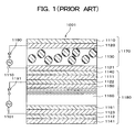
- FIG. 1 is a schematic sectional view showing a first conventional viewing-angle-controlled liquid crystal display device described in Japanese Laid-open Patent Application No. 5-72529.
- the first viewing-angle-controlled liquid crystal display device 1001 is composed of a liquid crystal element 1170 that is capable of controlling scattering; and a liquid crystal element 1180 that is capable of controlling optical rotation and double refraction properties.
- the liquid crystal element 1170 capable of controlling scattering is composed of substrates 1110 and 1111 that are optically transparent in the visible region, transparent electrodes 1120 and 1121 , a scattering liquid crystal 1130 , a voltage supply source 1100 , and a switch 1190 .
- the liquid crystal element 1180 capable of controlling optical rotation and double refraction properties is composed of substrates 1111 and 1112 that are optically transparent in the visible region, transparent electrodes 1122 and 1123 , polarizers 1140 and 1141 , orientation films 1150 and 1151 , a liquid crystal layer 1160 having optical rotation and double refraction properties, a voltage supply source 1101 , and a switch 1191 .
- Polymer dispersed liquid crystal is used as the scattering liquid crystal 1130
- TN liquid crystal is used as the liquid crystal 1180 that is capable of controlling optical rotation and double refraction properties.
- the polarizers 1140 and 1141 are arranged as a crossed Nicol.
- a voltage is applied between the transparent electrodes 1122 and 1123 , whereby the optical rotation and double refraction properties of the liquid crystal layer 1160 are changed, and this change can be used to control the transmittance of light.
- the optical rotation and double refraction properties that substantially affect the incident light will differ according to the direction of the viewing angle. A phenomenon therefore occurs in which the luminance and chroma are reduced or inverted, depending on the viewing angle.
- a liquid crystal element 1170 that can control scattering is disposed above this type of viewing-angle-dependent liquid crystal element 1180 to reduce viewing angle dependency.
- the liquid crystal molecules are randomly oriented in the absence of an electric field applied to the liquid crystal 1130 of the liquid crystal element 1170 that can control scattering, substantially isotropic scattering occurs over the entire viewing angle range, and a display can be obtained that has minimal dependency on the viewing angle.
- an electric field is applied to the liquid crystal 1130
- the liquid crystal molecules orient themselves substantially parallel to the applied electric field. The light emitted from the liquid crystal element 1180 exits without being scattered by the liquid crystal molecules.
- FIG. 2 is a schematic sectional view showing a second conventional viewing-angle-controlled liquid crystal display device described in Japanese Laid-open Patent Application No. 9-244018; and FIG. 3 is a schematic perspective view showing the illumination device used in this viewing-angle-controlled liquid crystal display device.
- the second conventional viewing-angle-controlled liquid crystal display device 2101 is composed of a liquid crystal display element 2102 , a scatter control element (scatter control means) 2103 , and an illumination device (backlight) 2104 .
- the scatter control element 2103 is disposed between the liquid crystal display element 2102 and the illumination device 2104 .
- FIG. 1 is a schematic sectional view showing a second conventional viewing-angle-controlled liquid crystal display device described in Japanese Laid-open Patent Application No. 9-244018
- FIG. 3 is a schematic perspective view showing the illumination device used in this viewing-angle-controlled liquid crystal display device.
- the second conventional viewing-angle-controlled liquid crystal display device 2101 is composed of a liquid crystal display element 2102 , a scatter
- the illumination device 2104 is provided with an opaque slitted sheet (translucent sheet) 2120 and an irradiating unit 2121 disposed on the substrate side of the scatter control element 2103 .
- a fluorescent tube or other light source 2122 is provided to the irradiating unit 2121 , and a light emission surface 2123 for emitting the light from the light source 2122 and guiding the light to the opaque slitted sheet 2120 is formed.
- a reflecting sheet 2124 for reflecting the light emitted from the light source 2122 is provided in the irradiating unit 2121 on the surface facing the light emission surface 2123 .
- the opaque slitted sheet 2120 a large number of linear opaque members extending in one direction are arranged parallel to each other on one surface of a translucent sheet. The extension direction of the opaque members coincides with the vertical direction of the display screen.
- the light emitted from the light source 2122 exits from the light emission surface 2123 of the irradiating unit 2121 , and is radiated to the scatter control element 2103 via the opaque slitted sheet 2120 .
- the opaque slitted sheet 2120 blocks light incident from directions that are significantly inclined with respect to the light-incident surface of the opaque slitted sheet 2120 . There is obtained thereby transmitted light that is highly parallel to the direction perpendicular to the plane of the opaque slitted sheet 2120 .
- the light emitted from the illumination device 2104 then is incident on the scatter control element 2103 .
- the scatter control element 2103 controls the scattering properties of incident light according to whether or not voltage is applied. When the scatter control element 2103 is in the scattering state, the light emitted from the illumination device 2104 is scattered by the scatter control element 2103 , whereas when the scatter control element 2103 is in the transparent state, the light from the illumination device 2104 is not scattered.
- this second conventional viewing-angle-controlled liquid crystal display device 2101 since scattering of the light can be controlled by the scatter control element 2103 , the viewing angle characteristics of displayed content can be controlled. Furthermore, since highly collimated light can be directed towards the liquid crystal display element 2102 by the illumination device 2104 , with the scatter control element 2103 in the transparent state, it is possible to reliably obtain viewing angle characteristics so that only an observer directly facing the display unit can ascertain the displayed content. Consequently, it is possible to obtain a liquid crystal display device that is capable of being switched at random between a state in which display characteristics are uniformly maintained in all viewing angle directions with negligible dependence of display characteristics on viewing angle, and a state in which displayed content can be ascertained only from a position directly facing the display unit.
- the conventional viewing-angle-controlled liquid crystal display devices described above have problems such as the following.
- the color of images changes when the viewing angle is switched.
- a switch is made from a narrow viewing angle display having a narrow viewing angle range to a wide viewing angle display having a wide viewing angle range
- images take on a yellowish hue, which can be unpleasant for the user.
- An object of the present invention is to provide a light source device that enables switching of the radiation angle range, wherein the light source device can prevent change in color when the radiation angle range is switched; a display device with switchable radiation angle range equipped with this light source device; a terminal device in which this display device is installed; a light source unit incorporating the light source device; and a method of driving the light source device.
- the light source device has a planar light source that emits light in planar form; a transparent/scattering switching element switchable between a transparent state in which light emitted from the planar light source is transmitted and a scattering state in which the light is scattered; and a control unit for controlling the planar light source and the transparent/scattering switching element; wherein during switching of the state of the transparent/scattering switching element, the control unit changes the chromaticity of light emitted from the planar light source, so as to reduce chromaticity change of light emitted from the transparent/scattering state switching element.
- control unit changes the chromaticity of the light emitted from the planar light source when the transparent/scattering switching element transitions from the transparent state to the scattering state, it is possible to cancel out chromaticity change caused by frequency-dependence of the scattering characteristics of the transparent/scattering switching element. It is thereby possible to reduce chromaticity change of light emitted from the transparent/scattering switching element.
- the control unit preferably controls the planar light source in such a way that the following Eqs. 1 to 3 are satisfied when the transparent/scattering switching element is switched, where the chromaticity coordinates of light emitted from the planar light source when the transparent/scattering switching element is brought to the transparent state are designated as (xt, yt), the chromaticity coordinates of light emitted from the transparent/scattering switching element are designated as (xpt, ypt), the chromaticity coordinates of light emitted from the transparent/scattering switching element when light having chromaticity coordinates (xt, yt) enters the transparent/scattering switching element while in the scattering state are designated as (xptd, yptd), the chromaticity coordinates of light emitted from the planar light source when the transparent/scattering switching element is in the scattering state are designated as (xd, yd), and the chromaticity coordinates of light emitted from the transparent
- the planar light source may have a first light source, and a second light source that emits light whose chromaticity coordinates are different from the chromaticity coordinates of the light emitted from the first light source; and the control unit may vary the proportion of the quantity of light emitted from the first light source and the quantity of light emitted from the second light source, so that when the transparent/scattering switching element is in the scattering state, this proportion is different from that in the transparent state.
- the chromaticity coordinate values of light emitted from the second light source may be smaller than the chromaticity coordinate values of light emitted from the first light source; and the control unit, when the transparent/scattering switching element is switched from the transparent state to the scattering state, may increase the quantity of light of the second light source so that the proportion of change in the quantity of light of the second light source is greater than the proportion of change in the quantity of light of the first light source.
- the second light source will emit light that is more bluish than the first light source, but since the transparent/scattering switching element in the scattering state scatters more of the short-wavelength component, the light emitted from the transparent/scattering switching element in the scattering state will maintain a white color close to that when in the transparent state.
- the first and second light sources are preferably light-emitting diodes.
- Light-emitting diodes are thinner than cold cathode fluorescent lamps, making it possible for the light source device to be thinner.
- Each of the light-emitting diodes may have a blue light-emitting diode that emits blue light, and a yellow phosphor that emits yellow light by excitation with the blue light.
- each light-emitting diode may have an ultraviolet light-emitting diode that emits ultraviolet light, a red phosphor that emits red light by excitation with the ultraviolet light, a green phosphor that emits green light by excitation with the ultraviolet light, and a blue phosphor that emits blue light by excitation with the ultraviolet light.
- the quantity of light of the light-emitting diode is preferably adjusted by pulse modulation. It is thereby possible to adjust the quantity of light by adjusting the emission time proportions, so that fluctuation in white balance can be reduced.
- the planar light source may have a light-guide plate for receiving light emitted from the first and second light sources, and emitting this light in planar form. There may be a plurality of first light sources and a plurality of second light sources arranged in alternating fashion. By so doing, a large number of light-emitting diodes can be placed in the planar light source, making it possible to increase the luminance of the light source device and reduce the occurrence of unevenness.
- the first light sources are preferably connected to each other in series, and the second light sources are preferably connected to each other in series. Electrical current flowing to the plurality of first light-emitting diodes can thereby be made mutually equal, and electrical current flowing to the plurality of second light emitting diodes can be made mutually equal. As a result, variability in quantity of light caused by variability of internal impedance of the light-emitting diodes can be reduced.
- the number of first light sources and the number of second light sources are preferably equal to each other.
- the driving voltages for the first and second light sources can be identical, and the design of the control unit can be simplified, thereby reducing cost, saving space, and improving reliability.
- the wiring terminals of the first light sources and the wiring terminals of the second light sources may be partially shared.
- a single first light source and a single second light source may be provided, and one corner of the light-guide plate may be cut off to form a single inclined surface, with the first and second light sources positioned at locations facing the inclined surface. It is thereby possible to reduce the occurrence of unevenness when a change is produced in the quantity of light of the first and second light sources.
- the planar light source may have a first light-guide plate for receiving light emitted from the first light source and emitting this light in planar form; and a second light-guide plate which, when viewed from the first light-guide plate, is disposed on the transparent/scattering switching element side or on the opposite side therefrom, and which receives light emitted from the second light source and emits this light in planar form.
- the first light source and the second light source device viewed in the direction looking toward the planar light source from the transparent/scattering switching element, are preferably positioned in the same mutual location relative to each other. The occurrence of unevenness can be reduced thereby.
- Each of the first and second light sources may be a cold cathode fluorescent lamp. It is thereby possible to attain a high-efficiency light source device. Light source devices furnished with cold cathode fluorescent lamps are more appropriate for installation in terminal devices larger than medium ones, rather than in small mobile terminal devices, and when so installed can reduce change in color during viewing angle switching.
- the first and second light sources may be housed in mutually different packages.
- ordinary light-emitting diodes merely having different chromaticity coordinates can be used, making it possible to lower costs.
- the light source device may have a light direction regulating element for regulating a direction of light emitted from the planar light source and emitting the light to the transparent/scattering switching element. By so doing, the directivity of light emitted from the planar light source can be increased.
- the display device comprises the aforementioned light source device, and a transmissive display panel for transmitting light emitted from this light source device, and thus superimposes an image on this light.
- the viewing angle of the display device can be switched.
- the transmissive display panel may be a liquid crystal panel.
- the liquid crystal panel is preferably in a horizontal field mode, multi-domain vertical alignment mode, or film-compensated TN mode liquid crystal panel. It is thereby possible to reduce grayscale inversion in the display when the transparent/scattering switching element is in the scattering state, so that visibility is improved.
- the terminal device has the aforementioned display device.
- This terminal device may be a mobile phone, a personal information terminal, a gaming device, a digital camera, a video camera, a video player, a notebook-type personal computer, a cash dispenser, or a vending machine.
- the light source unit comprises a planar light source that emits light in planar form; and a transparent/scattering switching element switchable between a transparent state in which light emitted from the planar light source is transmitted and a scattering state in which the light is scattered; wherein during switching of the state of the transparent/scattering switching element, the chromaticity of light emitted from the planar light source is changed so as to reduce chromaticity change of light emitted from the transparent/scattering state switching element.
- the method for driving a light source device comprises a transparent step for emitting first light by a planar light source that emits light in planar form, and switching to a transparent state a transparent/scattering switching element switchable between a transparent state in which light emitted from the planar light source is transmitted, and a scattering state in which the light is scattered; and a scattering step for causing the planar light source to emit second light whose chromaticity differs from the chromaticity of the first light, and switching the transparent/scattering switching element to the scattering state; wherein the chromaticity of the second light is set so as to reduce chromaticity change of light emitted from the transparent/scattering switching element during transition from the transparent step or the scattering step to the other.
- FIG. 1 is a schematic sectional view showing the first conventional viewing-angle-controlled liquid crystal display device disclosed in Japanese Laid-open Patent Application 5-72529;
- FIG. 2 is a schematic sectional view showing the first conventional viewing-angle-controlled liquid crystal display device disclosed in Japanese Laid-open Patent Application 9-244018;
- FIG. 3 is a schematic perspective view showing the illumination device used in the conventional viewing-angle-controlled liquid crystal display device disclosed in Japanese Laid-open Patent Application 9-244018;
- FIG. 4 is a perspective view showing the display device according to a first embodiment of the present invention.
- FIG. 5 is a perspective view showing a light source unit as a constituent element thereof
- FIG. 6 is an xy chromaticity diagram depicting the chromaticity coordinates (x, y) of two types of light sources which are constituent elements of the light source unit;
- FIG. 7 is a sectional view showing a light source, light-guide plate, and optical film as constituent elements of the light source unit;
- FIG. 8 is a sectional view showing the transparent/scattering state switching element that is a constituent element of the light source unit
- FIG. 9 is an xy chromaticity diagram depicting chromaticity coordinates (x, y) with the transparent/scattering switching element in the transparent state and in the scattering state;
- FIG. 10 is a perspective view showing the terminal device according to the present embodiment.
- FIGS. 11A through 11G are timing charts depicting operation when the display device according to the present embodiment is switched from a narrow-angle display to a wide-angle display, wherein time is plotted on the horizontal axis of each chart.
- FIG. 11A has the haze (HAZE: haze value) of the transparent/scattering state switching element plotted on the vertical axis
- FIG. 11B has the emission luminosity of the white LED plotted on the vertical axis
- FIG. 11C has the emission luminosity of the bluish white LED plotted on the vertical axis
- FIG. 11D has the frontal luminance of light prior to entering the transparent/scattering switching element plotted on the vertical axis
- FIG. 11A has the haze (HAZE: haze value) of the transparent/scattering state switching element plotted on the vertical axis
- FIG. 11B has the emission luminosity of the white LED plotted on the vertical axis
- FIG. 11C has the emission luminos
- FIG. 11E has the chromaticity coordinate (x, y) values of light prior to entering the transparent/scattering switching element plotted on the vertical axis
- FIG. 11F has the frontal luminance of light after entering the transparent/scattering switching element plotted on the vertical axis
- FIG. 11G has the chromaticity coordinate (x, y) values of light after entering the transparent/scattering switching element plotted on the vertical axis;
- FIG. 12 is a perspective view showing the display device according to a second embodiment of the invention.
- FIG. 13 is a perspective view showing a light source unit as a constituent element thereof
- FIG. 14 is a perspective view showing a louver as a constituent element thereof
- FIG. 15 is a perspective view showing the display device according to a third embodiment of the invention.
- FIGS. 16A through 16G are timing charts depicting operation when the display device according to the present embodiment is switched from a narrow-angle display to a wide-angle display, wherein time is plotted on the horizontal axis of each chart.
- FIG. 16A has the haze (HAZE: haze value) of the transparent/scattering state switching element plotted on the vertical axis
- FIG. 16B has the emission luminosity of the white LED plotted on the vertical axis
- FIG. 16C has the emission luminosity of the bluish white LED plotted on the vertical axis
- FIG. 16D has the frontal luminance of light prior to entering the transparent/scattering switching element plotted on the vertical axis
- FIG. 16E has the chromaticity coordinate (x, y) values of light prior to entering the transparent/scattering switching element plotted on the vertical axis
- FIG. 16F has the frontal luminance of light after entering the transparent/scattering switching element plotted on the vertical axis
- FIG. 16G has the chromaticity coordinate (x, y) values of light after entering the transparent/scattering switching element plotted on the vertical axis;
- FIG. 17 is a perspective view showing the display device according to a fifth embodiment of the invention.
- FIG. 18 is a perspective view showing the display device according to a sixth embodiment of the invention.
- FIG. 19 is a perspective view showing a light source unit as a constituent element thereof.
- FIG. 20 is a perspective view showing a light source, light-guide plate, and optical film as constituent elements of the light source unit;
- FIG. 21 is a sectional view showing a light source, light-guide plate, and optical film as constituent elements of the light source unit;
- FIG. 22 is a perspective view showing the display device according to a seventh embodiment of the invention.
- FIG. 23 is a perspective view showing a light source unit as a constituent element thereof.
- FIG. 24 is a perspective view showing a light source, light-guide plate, and optical film as constituent elements of the light source unit;
- FIG. 25 is a sectional view showing a light source, light-guide plate, and optical film as constituent elements of the light source unit;
- FIG. 26 is a perspective view showing the display device according to an eighth embodiment of the invention.
- FIG. 27 is a perspective view showing a light source unit as a constituent element thereof.
- FIG. 28 is a sectional view showing a light source, light-guide plate, and optical film as constituent elements of the light source unit;
- FIG. 29 is a partly enlarged sectional view depicting the behavior of light in proximity to a convex portion of the optical film
- FIG. 30 is a perspective view showing the convex portion of the optical film
- FIG. 31 is a perspective view showing the terminal device according to the present embodiment.
- FIG. 32 is a perspective view showing the display device according to a ninth embodiment of the invention.
- FIG. 33 is a perspective view showing a light source unit as a constituent element thereof.
- FIGS. 34A through 34F are timing charts depicting operation when the display device according to the present embodiment is switched from a narrow-angle display to a wide-angle display, wherein time is plotted on the horizontal axis of each chart.
- FIG. 34A has the haze (HAZE: haze value) of the transparent/scattering state switching element plotted on the vertical axis
- FIG. 34B has the emission luminosity of the white LED plotted on the vertical axis
- FIG. 34C has the frontal luminance of light prior to entering the transparent/scattering switching element plotted on the vertical axis
- FIG. 34D has the chromaticity coordinate (x, y) values of light prior to entering the transparent/scattering switching element plotted on the vertical axis
- FIG. 34E has the frontal luminance of light after entering the transparent/scattering switching element plotted on the vertical axis
- FIG. 34F has the chromaticity coordinate (x, y) values of light after entering the transparent/scattering switching element plotted on the vertical axis.
- FIG. 4 is a perspective view showing the display device according to the present embodiment
- FIG. 5 is a perspective view showing a light source unit as a constituent element thereof
- FIG. 6 is an xy chromaticity diagram depicting the chromaticity coordinates (x, y) of two types of light sources which are constituent elements of this light source unit;
- FIG. 4 is a perspective view showing the display device according to the present embodiment
- FIG. 5 is a perspective view showing a light source unit as a constituent element thereof
- FIG. 6 is an xy chromaticity diagram depicting the chromaticity coordinates (x, y) of two types of light sources which are constituent elements of this light source unit
- FIG. 4 is a perspective view showing the display device according to the present embodiment
- FIG. 5 is a perspective view showing a light source unit as a constituent element thereof
- FIG. 6 is an xy chromaticity diagram depicting the chromaticity coordinates (x, y) of two types of light sources which are constituent elements of this
- FIG. 7 is a sectional view showing a light source, light-guide plate, and optical film as constituent elements of the light source unit;
- FIG. 8 is a sectional view showing the transparent/scattering state switching element that is a constituent element of the light source unit;
- FIG. 9 is an xy chromaticity diagram depicting chromaticity coordinates (x, y) with the transparent/scattering switching element in the transparent state and in the scattering state;
- FIG. 10 is a perspective view showing the terminal device according to the present embodiment.
- the display device 2 is composed of a light source device 1 and a transmissive liquid crystal panel 7 .
- a light-guide plate 3 consisting of transparent material is disposed in the light source device 1 .
- the light-guide plate 3 is of rectangular plate shape.
- a plurality of these white LEDs 51 and bluish white LEDs 52 are arranged along the light-incident surface 3 a of the light-guide plate 3 .
- the white LEDs 51 number three and the bluish white LEDs 52 number two.
- the white LEDs 51 and the bluish white LEDs 52 are arranged in alternating fashion so that LEDs of different types are situated adjacently.
- Light incident on the light-incident surface 3 a is output uniformly by the light-guide plate 3 from its principal face (light-emitting surface 3 b ).
- An optical film 4 is disposed on the light-emitting surface 3 b side of the light-guide plate 3 .
- the purpose of the optical film 4 is to cause light exiting the light-guide plate 3 to be reflected towards the direction of the normal line of the light-emitting surface of the light-guide plate 3 .
- a transparent/scattering switching element 122 is disposed to the light-emitting surface side of the optical film 4 . The transparent/scattering switching element 122 , during exit from the opposite side thereof of light entering from the optical film 4 , switches between a state of scattering the light, and a state of transmitting the light without scattering.
- a control circuit 201 for controlling the white LEDs 51 , the bluish white LEDs 52 , and the transparent/scattering switching element 122 is also provided.
- This control circuit 201 adjusts the luminosity of the white LEDs 51 and the bluish white LEDs 52 by controlling the amount of current.
- the white LEDs 51 , the bluish white LEDs 52 , the light-guide plate 3 , the optical film 4 , the transparent/scattering switching element 122 , and the control circuit 201 together constitute the light source device 1 .
- the transmissive liquid crystal panel 7 is disposed on the light-emitting surface side of the transparent/scattering switching element 122 , and is allowed to transmit light, whereby an image is superimposed on the light.
- the white LEDs 51 , the bluish white LEDs 52 , the light-guide plate 3 , the optical film 4 , and the transparent/scattering switching element 122 together constitute the light source unit 6 . That is, the light source device 1 (see FIG. 4 ) is composed of the light source unit 6 and the control circuit 201 .
- an XYZ orthogonal coordinate system is established as follows in the present specification.
- the direction going from the white LEDs 51 and bluish white LEDs 52 towards the light-guide plate 3 interior is designated as the +X direction, and the opposite direction as the ⁇ X direction.
- the +X direction and ⁇ X direction are collectively referred to as the X-axis direction.
- the one orthogonal to the X-axis direction is designated as the Y-axis direction.
- the direction orthogonal to both the X-axis direction and the Y-axis direction is designated as the Z-axis direction; within this Z-axis direction, the direction going from the light-guide plate 3 interior towards the light-emitting surface 3 b is designated as the +Z direction, and the opposite direction as the ⁇ Z direction.
- the +Z direction represents the forward direction, i.e., going towards the user.
- the +Y direction represents the direction forming a right-handed coordinate system. That is, with the thumb of the right hand pointing in the +X direction and the index finger in the +Y direction, the middle finger points in the +Z direction.
- the light-emitting surface 3 b of the light-guide plate 3 represents the XY plane, and viewed from the light-guide plate 3 , the white LEDs 51 and bluish white LEDs 52 are situated in the ⁇ X direction, and the optical film 4 is disposed in the +Z direction.
- the transparent/scattering switching element 122 is disposed in the +Z direction viewed from the optical film 4 .
- the white LEDs 51 and bluish white LEDs 52 constituting the two different types of light sources are LEDs that are composed of a blue LED and a yellow phosphor for emitting yellow light by excitation with the blue light emitted from this blue LED, and that emit white light by excitation with blue and yellow light. LEDs that operate on this principle emit white light of a slightly different color depending on the luminosity of the bluish white LED and the intensity of the yellow light emitted from the yellow phosphor. Specifically, white light is obtained where there is balance between the blue light emitted from the blue LED and the yellow light emitted from the yellow phosphor.
- Bluish white light is emitted in cases in which the blue light emitted from the blue LED is more intense than the yellow light emitted from the yellow phosphor.
- the white LEDs 51 represent the former LEDs that emit white light
- the bluish white LEDs 52 represent the latter LEDs that emit bluish white light.
- the light source unit 6 is furnished with three white LEDs 51 and two bluish white LEDs 52 , and the LEDs of the same type are connected in series. That is, the three white LEDs 51 are connected in series, and the two bluish white LEDs 52 are connected in series.
- FIG. 7 is a sectional view of the light-guide plate 3 and the optical film 4 along line A-A′ in FIG. 5 .
- An example of a light path is also shown in FIG. 7 ; this will be described later.
- a diffusion pattern is formed on the light-incident surface 3 a , in order to reduce in-plane irregular luminance at the light-emitting surface 3 b caused by LED placement location.
- an inclined surface 3 d is formed on the light-emitting surface 3 b of the light-guide plate 3 .
- the inclined surface 3 d is inclined in the direction of illumination of light that has been emitted from the white LEDs 51 and bluish white LEDs 52 , and transmitted by the light-guide plate 3 in the +X direction.
- the incline angle of the inclined surface 3 d is six degrees with respect to the X-axis direction, for example.
- a plurality of inclined surfaces 3 d are arrayed in the X-axis direction, with each inclined surface extending over the entire length of the light-guide plate 3 in the Y-axis direction.
- a hologram pattern (not shown) having anisotropy within the XY plate is formed on the light-emitting surface 3 b of the light-guide plate. Light propagated within the light-guide plate 3 and emitted from the light-emitting surface 3 b is imparted with increased directivity in the Y-axis direction by means of this hologram pattern.
- the optical film 4 is composed of a flat plate portion 4 a , and a plurality of primary prism elements 4 b formed on the flat plate portion 4 a on the side facing the light-guide plate 3 .
- the primary prism elements 4 b are prism elements that project out in the ⁇ Z direction with their ridgelines extending in the Y-axis direction; a plurality of these primary prism elements 4 b are arrayed along the X-axis direction.
- the apex angle of the primary prism elements 4 b is set to 70 degrees, for example.
- the Z-axis direction matches the direction of projection of the primary prism elements 4 b ; i.e., the direction that is parallel to a plane dividing the side faces of the primary prism elements 4 b in to two equal parts and that is orthogonal to the Y-axis direction.
- the optical film 4 having the primary prism elements 4 b formed thereon causes light emitted from the light-guide plate 3 to be deflected toward the +Z direction within the XZ plane, so that the light exits with high directivity in the +Z direction.
- the hologram pattern formed on the light-emitting surface 3 b of the light-guide plate functions to increase directivity in the Y-axis direction, so light exiting the optical film 4 has heightened directivity in the +Z direction, in relation to both the X-axis direction and the Y-axis direction.
- the material for the light-guide plate 3 and the optical film 4 is preferably a clear resin due to the ease of processing afforded thereby.
- PMMA polymethyl-methacrylate having a refractive index of 1.5 is used.
- FIG. 8 is a sectional view showing the transparent/scattering state switching element 122 disposed on the light-emitting surface side of the optical film 4 .
- a pair of transparent substrates 109 arranged parallel to one another, with each transparent substrate 109 having an electrode 110 disposed on the face thereof facing towards the other transparent substrate 109 , so as to cover the face of the transparent substrate 109 .
- a PDLC Polymer Dispersed Liquid Crystal
- liquid crystal molecules 111 b are dispersed throughout a polymer matrix 111 a .
- the PDLC layer 111 is formed, for example, by exposing a mixture of photosetting resin and a liquid crystal material to bring about setting.
- the orientation of the liquid crystal molecules 111 b within the PDLC layer 111 is changed through application of a voltage to the PDLC layer 111 by using the pair of electrodes 110 .
- a voltage for example, in the absence of an electric field applied to the PDLC layer, since the apparent refractive indices of the polymer matrix and the liquid crystal molecules differ, incident light is scattered and caused to exit in a scattered state.
- an electric field is applied to the PDLC layer, the apparent refractive indices of the polymer matrix and the liquid crystal molecules become substantially identical, and a transparent state is established in which the incident light is emitted without being scattered.
- the transparent/scattering switching element 122 thus scatters or transmits incident light and emits the light to the transmissive liquid crystal panel 7 .
- a 60 Hz rectangular wave is applied to the transparent/scattering switching element in order to prevent burn-in.
- control circuit 201 is connected to the transparent/scattering switching element 122 and to the white LEDs 51 and bluish white LEDs 52 mentioned previously, and is used to drive and control the transparent/scattering switching element and the LEDs.
- the display device 2 is installed in a mobile phone 9 , for example.
- the mobile phone 9 used as a mobile terminal in accordance with the present embodiment is provided with the above-described display device 2 .
- FIGS. 11A through 11G are timing charts depicting operation when the display device according to the present embodiment is switched from a narrow-angle display to a wide-angle display, wherein time is plotted on the horizontal axis of each chart.
- FIG. 11A has the haze (HAZE: haze value) of the transparent/scattering state switching element plotted on the vertical axis
- FIG. 11B has the emission luminosity of the white LED plotted on the vertical axis
- FIG. 11C has the emission luminosity of the bluish white LED plotted on the vertical axis
- FIG. 11A has the haze (HAZE: haze
- FIG. 11D has the frontal luminance of light prior to entering the transparent/scattering switching element plotted on the vertical axis
- FIG. 11E has the chromaticity coordinate (x, y) values of light prior to entering the transparent/scattering switching element plotted on the vertical axis
- FIG. 11F has the frontal luminance of light after entering the transparent/scattering switching element plotted on the vertical axis
- FIG. 11G has the chromaticity coordinate (x, y) values of light after entering the transparent/scattering switching element plotted on the vertical axis.
- control circuit 201 When the control circuit 201 receives a wide-angle display instruction, it drives the white LEDs 51 and the bluish white LEDs 52 so that they emit light, and drives the transparent/scattering switching element 122 so that it assumes the scattering state. As a result, the white LEDs 51 and the bluish white LEDs 52 light up, and the light emitted from the white LEDs 51 and the bluish white LEDs 52 enters the light-guide plate 3 from the light-incident face 3 a of the light-guide plate.
- the light that has entered the light-guide plate is diffused in the Y-axis direction within the light-guide plate, whereby the light of the white LEDs 51 and the bluish white LEDs 52 becomes mixed.
- the angle thereof with respect to the Z-axis direction is 48.2°. Since this angle is greater than the critical angle of 41.8°, the light is totally reflected without exiting from the light-guide plate 3 .
- the light-diffusing surface 3 c as well, light incident on areas other than the inclined surface 3 d is totally reflected at the same angle, so that the light is propagated in the direction away from the white LEDs 51 and the bluish white LEDs 52 while undergoing repeated total reflection between the light-emitting surface 3 b and the light-diffusing surface 3 c .
- light incident on the light-guide plate 3 will always have an angle of 41.8° or less with respect to the Z-axis direction, subsequent to incidence. Consequently, the incident light will have an angle of 48.2° or greater with respect to the Z-axis direction when reaching the light-emitting surface 3 b or the light-diffusing surface 3 c of the light-guide plate 3 , and will be totally reflected.
- Light L 1 that has exited from the light-guide plate 3 at an incline angle of 62.4° with respect to the Z-axis direction is now incident on the optical film 4 . Since the apex angle of the primary prism elements 4 b is 70°, the angle of incidence on the primary prism element 4 b is 7.4°, and an angle of 4.9° is formed by the direction of advance of incident light within the primary prism element 4 b and the normal line of the conical incident face. Light L 1 subsequently reaches the side face on the opposite side of the primary prism element 4 b , but since the angle thereof with respect to this side face is 65.1° from the plane normal line, it is totally reflected and advances in a direction 11.1° from the Z-axis.
- the angle of the light L 1 exiting from the optical film 4 is a direction 16.8° from the Z-axis. That is, light exiting the optical film 4 has strong directivity in essentially the Z-axis direction within the XZ plane.
- the light emitted from the optical film 4 is now incident on the transparent/scattering switching element 122 . Since the transparent/scattering switching element 122 is in the scattering state in the absence of applied voltage, the high-directivity light is scattered uniformly by the transparent/scattering switching element 122 , and is thereby dispersed over a wide angle range. That is, the light is scattered by the transparent/scattering switching element 122 , directivity is reduced, and wide-angle light is generated. The light distributed over this wide range is incident on the transmissive liquid crystal panel 7 which imposes an image, and the light then exits while maintaining a wide angle. In this way, the image is displayed over a wide viewing angle.
- the control circuit 201 When the control circuit 201 receives a narrow-angle display instruction, it drives the white LEDs 51 so that they emit light, as well as driving the transparent/scattering switching element 122 so that it is brought to the transparent state. As a result, only the white LEDs 51 light up, and the light emitted from the white LEDs 51 propagates through the light-guide plate 3 and exits from the optical film 4 in a narrow angle range, in the same manner as with wide-angle display. This light is incident on the transparent/scattering switching element 122 .
- the transparent/scattering switching element 122 Since the transparent/scattering switching element 122 is in the transparent state when voltage is applied thereto, the high-directivity light is transmitted unchanged, without being scattered by the transparent/scattering switching element 122 . That is, the light exits the transparent/scattering switching element 122 while maintaining high directivity.
- the light having the high-directivity distribution is incident on the transmissive liquid crystal panel 7 to superpose an image, and the light then exits while maintaining high directivity. In this way, the image is displayed over a narrow viewing angle.
- the transparent/scattering switching element 122 is disposed between the optical film 4 and the transmissive liquid crystal panel 7 , and the transparent/scattering switching element 122 is furnished with a PDLC layer 111 so that the light radiation angle can be switched by transmission or scattering of light by the PDLC layer 111 .
- the extent of scattering of light depends on the wavelength of the light, with light of shorter wavelength being scattered more strongly, and light of longer wavelength being more difficult to scatter.
- the color change differs according to the fine structure and thickness of the transparent/scattering switching element.
- haze of the transparent/scattering switching element is increased, in association with which the quantity of light of the bluish white LEDs 52 is increased. That is, in the narrow-viewing-angle display mode up to time t 1 , only the white LEDs 51 are lit, whereas in the wide-viewing-angle display mode beginning at time t 1 , both the white LEDs 51 and the bluish white LEDs 52 are lit. It is thereby possible to prevent the phenomenon of a drop in frontal luminance during switching from a narrow-viewing-angle display mode to a wide-viewing-angle display mode, as shown in FIGS. 11 d and 11 f.
- the chromaticity coordinates of light emitted from the transparent/scattering switching element can be kept the same in both the narrow-viewing-angle display mode prior to time t 1 and the wide-viewing-angle display mode beginning at time t 1 .
- the phenomenon whereby the display takes on a yellowish hue unpleasant for the user can be reduced during switching from a narrow-viewing-angle display mode to a wide-viewing-angle display mode.
- the display device 2 is switched from a narrow-viewing-angle display to a wide-viewing-angle display was described above, but the same principle is applicable to the case of switching from a wide-viewing-angle display to a narrow-viewing-angle display.
- the present embodiment is effective for preventing the phenomenon of yellow discoloration of the display during switching from a narrow-viewing-angle display to a wide-viewing-angle display.
- control circuit 201 controls the white LEDs 51 and the bluish white LEDs 52 in such a way that the following Eqs.
- the chromaticity coordinates of light emitted from the light-guide plate 3 i.e., of the mixed light emitted from the three white LEDs 51 and the two bluish white LEDs 52 (hereinafter termed “mixed light”) when the transparent/scattering switching element 122 is placed in the transparent state, are designated as (xt, yt)
- the chromaticity coordinates of light emitted from the transparent/scattering switching element are designated as (xpt, ypt)
- the chromaticity coordinates of light emitted from the transparent/scattering switching element when the light-source light having chromaticity coordinates (xt, yt) enters the transparent/scattering switching element while the element is in the scattering state are designated as (xptd, yptd)
- the chromaticity coordinates of the light source with the transparent/scattering switching element in the scattering state are designated as (xd, yd)
- Eqs. 4 to 6 are identical expressions to Eqs. 1 to 3 given previously.
- Light whose aforementioned chromaticity coordinates are (xt, yt) represents light-source light that is always emitted by the light-guide plate in conventional light source devices, as well as light-source light that is emitted from the light-guide plate solely during a narrow-angle display in the present embodiment.
- Light whose aforementioned chromaticity coordinates are (xpt, ypt) represents light that is emitted from the transparent/scattering switching element 122 during a narrow-angle display in conventional light source devices and in the light source device of the present embodiment.
- Light whose aforementioned chromaticity coordinates are (xptd, yptd) represents light emitted from the transparent/scattering switching element during a wide-angle display in conventional light source devices.
- Light whose chromaticity coordinates are (xd, yd) represents light-source light emitted from the light-guide plate during a wide-angle display in the light source device of the present embodiment.
- Eq. 6 means that, based on the chromaticity coordinates (xpt, ypt), the chromaticity coordinates (xpd, ypd) are located closer to the chromaticity coordinates (xpt, ypt) than to the chromaticity coordinates (xptd, yptd).
- the color appearance of the light will be closer to that in the case in which light-source light during a narrow-angle display has passed through the transparent/scattering switching element in the transparent state.
- the effects of the present embodiment shall be described.
- haze of the transparent/scattering switching element is increased, in association with which the quantity of light of the bluish white LEDs 52 is increased, thereby making smaller the chromaticity coordinates of the light-source light so that the light is bluish.
- the transparent/scattering switching element in the scattering state produces greater scattering of the short-wavelength component. Therefore, if the color of the light source remains the same during a narrow-angle display and wide-angle display, the light exiting the transparent/scattering switching element will have a yellowish tinge.
- the light source by giving the light source a bluish hue during a wide-angle display, it is possible to maintain the light at the same white color as during a narrow-angle display. Also, by increasing the quantity of light of the bluish white LEDs during a wide-angle display in addition to the lighting of the white LEDs, frontal luminance can be maintained at the same level as during a narrow-angle display.
- the white LEDs and the bluish white LEDs in alternating fashion, the occurrence of irregular luminance can be reduced, even where the drive conditions of the respective LEDs differ between a narrow-angle display and a wide-angle display.
- all of the white LEDs are connected in series, and all of the bluish white LEDs are connected in series.
- the present embodiment describes the use of LEDs of two types, namely, white LEDs and bluish white LEDs, as the light sources, the invention is not limited thereto, and it is also possible to employ any combination whereby the chromaticity coordinates of the light source can be varied between a narrow-angle display and a wide-angle display. As a result, it is possible to reduce the color change of light exiting the transparent/scattering switching element. It is acceptable to use LEDs of three or more types.
- an LED of a type composed of a blue LED and a yellow phosphor that emits yellow light by excitation with the blue light emitted from the blue LED is used as an LED.
- the invention is not limited thereto, and can also be implemented effectively for a light source that emits fixed proportions of light whose wavelengths can be easily scattered by the transparent/scattering switching element in a scattering state, and light that has other wavelengths, so that the spectral balance of the emitted light cannot be varied freely through driving conditions or the like.
- Such a light source is an LED of a type composed of an ultraviolet LED that emits ultraviolet light, and red/blue/green phosphors that emit red/blue/green light by excitation with the ultraviolet light emitted from the ultraviolet LED.
- the emission proportion of red/blue/green is fixed depending on the amount of the individual red/blue/green phosphors, but by using LEDs with an increased amount of blue phosphor as the bluish white LEDs, effects analogous to the present embodiment can be obtained.
- LEDs of the type composed of an ultraviolet LED and red/blue/green phosphors are used, it is possible to display more vivid colors and to improve color rendering, as compared to the use of LEDs of a type composed of a blue LED and a yellow phosphor that emits yellow light by excitation with the blue light emitted from the blue LED.
- Change in color during switching between a narrow-angle display and a wide-angle display can also be reduced by using a light source device that employs a light source whose emission proportions of various wavelength bands can be controlled through driving conditions or the like.
- a light source is an LED containing red/blue/green colors in a single package, with each color being controlled independently.
- the use of such a light source requires major control circuitry, and the cost of the light source will thus be higher.
- the present embodiment allows the control circuitry to be simplified and costs to be reduced because it is sufficient merely to use a plurality of types of light sources whose emission proportion are fixed depending on the wavelength, and to control the emission level of the light sources of each type.
- the white LED set composed of three serially connected white LEDs and the bluish white LED set composed of two serially connected bluish white LEDs may share either cathode or anode terminals. By so doing, three lines, rather than four, from the light source will suffice, making it possible to conserve space.
- the white LEDs and bluish white LEDs are preferably contained in mutually different packages. Costs can thereby be reduced since ordinary light-emitting diodes having mutually different chromaticity coordinates can merely be used.
- the transparent/scattering switching element is not limited to one provided with a PDLC layer, it being possible to use any element switchable between a transparent state and a scattering state.
- a PDLC layer is one that assumes the scattering state in the absence of applied voltage, and assumes the transparent state when a voltage is applied.
- the intensity of the light source during the scattering state can be enhanced without increasing the battery capacity, since the transparent/scattering state switching element no longer consumes power when in the scattering state, and the power that would have been consumed can be allocated to the light source.
- a PDLC layer that assumes the transparent state in the absence of applied voltage, and the scattering state when a voltage is applied.
- This type of PDLC layer can be fabricated by exposing a polymer matrix to light to cure the polymer matrix while applying a voltage. By this configuration, there is no need to apply a voltage to the PDLC layer, so power consumption can be reduced in a mobile information terminal in which narrow-angle display is frequently used.
- Cholesteric liquid crystals, ferroelectric liquid crystals, or the like may also be used as the liquid crystal molecules of the PDLC layer. Even when voltage is no longer applied, these liquid crystals retain the same orientation as when the voltage was applied, i.e., the crystals have memory properties. By using this type of PDLC layer, it becomes possible to reduce power consumption.
- the display panel used in combination with the planar light source device of the present invention is not limited to a liquid crystal panel, and any display panel that uses a light source device may be used.
- the liquid crystal panel is also not limited to transmissive type, and any panel that has a transmissive area in each pixel may be used.
- a transflective liquid crystal panel having a reflective area in a portion of each pixel, a micro-transmissive transflective liquid crystal panel, or a micro-reflective liquid crystal panel may also be used.
- a liquid crystal panel is preferred that has minimal dependence on the viewing angle. Grayscale inversion during display at a wide viewing angle can thereby be reduced.
- Examples of the mode of such a liquid crystal panel include the horizontal field mode IPS (In-Plane Switching), FFS (Fringe Field Switching), AFFS (Advanced Fringe Field Switching), and the like.
- Vertical alignment modes include MVA (Multi-domain Vertical Alignment), which is multi-domain and has reduced viewing-angle dependency, as well as PVA (Patterned Vertical Alignment), ASV (Advanced Super V), and the like.
- a film-compensated TN mode liquid crystal display panel may also be appropriately used.
- a mobile phone was described as the terminal device, but the invention is not limited thereto, and the display device according to the present embodiment can also be implemented suitably not only in a mobile phone, but in various other kinds of terminal devices such as PDAs (Personal Digital Assistant: personal information terminal), gaming devices, digital cameras, digital video cameras, and various other types of mobile terminal devices.
- the display device according to the present embodiment may be implemented not only in mobile terminal devices, but also in notebook-type personal computers, cash dispensers, vending machines, and other various types of terminal devices.
- FIG. 12 is a perspective view showing the display device according to the present embodiment of the invention.
- FIG. 13 is a perspective view showing a light source unit as a constituent element thereof; and
- FIG. 14 is a perspective view showing a louver as a constituent element thereof and which constitutes a light direction regulating element.
- a characteristic feature of the display device 21 , light source device 11 , and light source unit 61 according to the second embodiment feature is that these devices have as a constituent element a louver 112 that constitutes a light direction regulating element.
- the louver 112 is positioned between the optical film 4 and the transparent/scattering switching element 122 .
- the louver 112 has transparent zones 112 a that transmit light, and absorbing zones 112 b that absorb light, arrayed in alternating fashion in a direction parallel to the louver surface.
- the direction in which the transparent zones 112 a and absorbing zones 112 b are arrayed in alternating fashion is the Y-axis direction in FIG. 12 .
- Other aspects in the present embodiment are similar to those in the first embodiment described previously.
- the louver 112 can increase the directivity in the Y-axis direction of light emitted from the optical film 4 .
- leakage of light in the diagonal direction during a narrow-angle display can be reduced, and the effect to prevent surreptitious viewing can be increased.
- FIG. 15 is a perspective view showing the display device according to this embodiment of the invention.
- the display device 22 , light source device 12 , and light source unit according to the third embodiment differ from the display device 2 , light source device 1 , and light source unit 6 according to the above-described first embodiment in that there are three serially connected bluish white LEDs, the same number as the white LEDs.
- the present embodiment is similar to the first embodiment described previously.
- the bluish white LEDs and the white LEDs are equal in number, and the LEDs of each type are connected in series so that the driving voltage may be the same for each.
- FIGS. 16A through 16G are timing charts depicting operation when the display device according to the present embodiment is switched from a narrow-angle display to a wide-angle display, wherein time is plotted on the horizontal axis of each chart.
- FIG. 16A has the haze (HAZE: haze value) of the transparent/scattering state switching element plotted on the vertical axis
- FIG. 16B has the emission luminosity of the white LED plotted on the vertical axis
- FIG. 16C has the emission luminosity of the bluish white LED plotted on the vertical axis
- FIG. 16D has the frontal luminance of light prior to entering the transparent/scattering switching element plotted on the vertical axis
- FIG. 16E has the chromaticity coordinate (x, y) values of light prior to entering the transparent/scattering switching element plotted on the vertical axis
- FIG. 11F has the frontal luminance of light after entering the transparent/scattering switching element plotted on the vertical axis
- FIG. 11G has the chromaticity coordinate (x, y) values of light after entering the transparent/scattering switching element plotted on the vertical axis.
- the present embodiment is the same as in the above-described third embodiment in terms of the design of the light source device, display device, terminal device, and light source unit.
- the present embodiment differs, however, in terms of the method of driving the light source device, and in particular the lighting status of the light source.
- the third embodiment described previously only the white LEDs are lit during a narrow-angle display, with the bluish white LEDs being extinguished; while both the white LEDs and the bluish white LEDs are lit during a wide-angle display.
- the bluish white LED emission luminosity is zero in a narrow-angle display.
- the bluish white LEDs are lit in a narrow-angle display as well.
- the bluish white LEDs 52 are lit even during a narrow-angle display up to time t 1 .
- the quantity of light from the bluish white LEDs 52 at this time is less than the quantity of light during a wide-angle display starting at time t 1 , and the quantity of light from the bluish white LEDs 52 increases in association with the increase in haze of the transparent/scattering switching element during switching from a narrow-angle display to a wide-angle display.
- the proportion of light emitted from the bluish white LEDs 52 to total emitted light during a wide-angle display is greater than the emission proportion in the third embodiment described previously.
- the chromaticity coordinates of light emitted from the transparent/scattering switching element can be kept the same between the narrow-angle display mode up to time t 1 and the wide-angle display mode starting at time t 1 . It is thereby possible to reduce the phenomenon of a yellowish appearance of the display and the resultant unpleasantness for the user when a switch is made from a narrow-angle display mode to a wide-angle display mode.
- FIG. 17 is a perspective view showing the display device according to the present embodiment of the invention.
- the display device 22 and the light source device 13 according to this fifth embodiment differ in that a control circuit 202 is provided in place of the control circuit 201 .
- the control circuit 201 adjusts the quantity of light of the white LEDs 51 and the bluish white LEDs 52 by controlling the amount of current.
- the control circuit 202 also adjusts the quantity of light through pulse width modulation of the electric current.
- the circuit increases the quantity of emitted light by lengthening the time interval of electric current pulses applied to the white LEDs 51 and the bluish white LEDs 52 , and reduces the quantity of emitted light by shortening this time interval.
- the present embodiment is similar to the first embodiment described previously.
- the yellow phosphor is excited by a portion of the blue light emitted from the blue LED, and emits yellow light, with the blue light and yellow light mixing to produce white light. Therefore, the proportion of light emission of blue light and yellow light may fluctuate when changes are induced in the quantity of light of the white LEDs and the bluish white LEDs by variations in the amount of electric current between a narrow-angle display and a wide-angle display.
- FIG. 18 is a perspective view showing the display device according to this embodiment.
- FIG. 19 is a perspective view showing a light source unit as a constituent element thereof;
- FIG. 20 is a perspective view showing a light source, light-guide plate, and optical film as constituent elements of the light source unit; and
- FIG. 21 is a sectional view thereof.
- the display device 24 , light source device 14 , and light source unit 64 according to this sixth embodiment differ by being provided with a light-guide plate 31 in place of the light-guide plate 3 , and being provided with an optical film 41 in place of the optical film 4 .
- One white LED 51 and one bluish white LED 52 are disposed in a corner of the light-guide plate 31 .
- the light-guide plate 31 in the display device of the present embodiment is formed with a generally rectangular plate shape from a transparent resin such as methacrylate resin, and has an inclined surface 31 d formed on a light-diffusing surface 31 c .
- the corner of the corner portion having the smallest X coordinate and Y coordinate is cut off on the diagonal, with this cut face constituting a light-incident surface 31 a .
- the one white LED 51 and one bluish white LED 52 are disposed at locations facing this light-incident surface 31 a .
- the direction of the normal line of the light-incident surface 31 a is a direction orthogonal to the Z-axis direction, and intersecting both the X-axis direction and Y-axis direction.
- the inclined surface 31 d formed on the light-diffusing surface 31 c of the light-guide plate 31 is arranged in a concentric circle pattern, centered on the location of the corner that was cut off to form the light-incident surface 31 a (hereinafter termed the “virtual corner point”).
- the inclined surface 31 d spreads in a fan shape centered on the virtual corner point, with the outer edge thereof extending in arcuate shape centered on the virtual corner point.
- the direction of maximum incline of each inclined surface 31 d location is the direction going towards the virtual corner point from that location.
- the virtual corner point corresponds to the center point of the white LED 51 and the bluish white LED 52 .
- the optical film 41 there are formed a plurality of primary prism elements 41 b situated on the light-guide plate 31 side of a flat plate portion 41 a .
- the primary prism elements 41 b extend in an arcuate shape centered on the virtual corner point, with the primary prism elements 41 b being arranged in a concentric circle pattern centered on the virtual corner point.
- the present embodiment is similar to the first embodiment described previously.
- light emitted from the white LED 51 and the bluish white LED 52 enters the light-guide plate 31 from the light-incident surface 31 a .
- Light entering the light-guide plate 31 from the light-incident surface 31 a while spreading out radially with the virtual corner point as the center, advances through the light-guide plate 31 while being totally reflected between the light-emitting surface 31 b and the light-diffusing surface 31 c of the light-guide plate 31 .
- the direction of maximum incline at each inclined surface 31 d location is the direction going towards the aforementioned virtual corner point from each location, as viewed from the Z-axis direction. Therefore, there is no change in the direction of advance of the light when viewed from the Z-axis direction despite the light being reflected by the inclined surface 31 d . Accordingly, light emitted from the light-emitting surface 31 b of the light-guide plate 31 has high directivity in relation to the direction that connects the virtual corner point and the light exit location on the light-emitting surface 31 b , but has low directivity in relation to the direction orthogonal to this direction.
- This light then undergoes refraction and total reflection within the primary prism elements 41 b of the optical film 41 , is deflected in the +Z direction, exits the optical film 41 with high directivity in the +Z direction, and is incident on the transparent/scattering switching element 122 . Subsequent operation is the same as in the first embodiment described previously.
- the white LED and the bluish white LED as light sources can be disposed in a relatively narrow area at one corner of the light-guide plate.
- irregular luminance and irregular color during switching the quantity of light of the bluish white LED can be reduced.
- FIG. 22 is a perspective view showing the display device according to this embodiment.
- FIG. 23 is a perspective view showing a light source unit as a constituent element thereof;
- FIG. 24 is a perspective view showing a light source, light-guide plate, and optical film as constituent elements of the light source unit; and
- FIG. 25 is a sectional view thereof.
- the display device 25 , light source device 15 , and light source unit 65 according to the seventh embodiment differ by being provided with a light-guide plate 32 in addition to the light-guide plate 31 .
- the light-guide plate 32 is arranged parallel to the light-guide plate 31 and spaced apart to the ⁇ Z axis side of the light-guide plate 31 , and a white LED 51 is disposed in a corner portion of the light-guide plate 31 , while a bluish white LED 52 is disposed in a corner portion of the light-guide plate 32 .
- the white LED 51 and the bluish white LED 52 are situated at the same location, viewed from the Z-axis direction.
- the constitution of the light-guide plate 32 is the same as that of the light-guide plate 31 .
- an inclined surface 31 d is formed on the light-diffusing surface 31 c of the light-guide plate 31
- a light-incident surface 31 a is formed in one corner portion of the light-guide plate 31
- the white LED 51 is disposed at a location facing this light-incident surface 31 a .
- the inclined surface 31 d spreads over a fan-shaped area centered on the white LED 51 , and is arrayed in an arcuate shape centered on the white LED 51 .
- the direction of maximum incline of each inclined surface 31 d location is coincident with the direction going towards the white LED 51 from each location.
- an inclined surface 32 d is formed on the light-diffusing surface 32 c of the light-guide plate 32 , a light-incident surface 32 a is formed in one corner portion of the light-guide plate 32 , and the bluish white LED 52 is disposed at a location facing this light-incident surface 32 a .
- the inclined surface 32 d spreads over a fan-shaped area centered on the bluish white LED 52 , and is arrayed in an arcuate shape centered on the bluish white LED 52 .
- the direction of maximum incline of each inclined surface 32 d location is coincident with the direction going towards the bluish white LED 52 from each location.
- this embodiment is analogous to the sixth embodiment described previously.
- light emitted from the white LED 51 enters the light-guide plate 31 from the light-incident surface 31 a .
- the light that has entered the light-guide plate 31 from the light-incident surface 31 a while spreading out radially within the light-guide plate 31 , advances through the light-guide plate 31 while being totally reflected between the light-emitting surface 31 b and the light-diffusing surface 31 c of the light-guide plate 31 .
- the light emitted from the light-emitting surface 31 b of the light-guide plate 31 has high directivity in relation to the direction connecting the white LED 51 with the light exit location on the light-emitting surface 31 b , but has low directivity in relation to the direction orthogonal to this direction.
- light emitted from the bluish white LED 52 enters the light-guide plate 32 from the light-incident surface 32 a .
- the light that has entered the light-guide plate 32 from the light-incident surface 32 a while spreading out radially within the light-guide plate 32 , advances through the light-guide plate 32 while being totally reflected between the light-emitting surface 32 b and the light-diffusing surface 32 c of the light-guide plate 32 .
- the light emitted from the light-emitting surface 32 b of the light-guide plate 32 has high directivity in relation to the direction that connects the bluish white LED 52 and the light exit location on the light-emitting surface 32 b , but has low directivity in relation to the direction orthogonal to this direction.
- Light emitted from the light-guide plate 31 with small spread and high directivity undergoes refraction and total reflection by the primary prism elements 41 b of the optical film 41 and is deflected in the +Z direction, and is output with high directivity in the +Z direction, whereupon it enters the transparent/scattering switching element 122 . Subsequent operation is analogous to that in the first embodiment described previously.
- the white LED and the bluish white LED can be disposed respectively on two light-guide plates arranged spaced apart in the Z-axis direction, these two types of LEDs can be disposed in a stacked configuration at identical locations on the light-guide plates.
- irregular luminance and irregular color during switching of the quantity of light of the bluish white LED can be reduced effectively.
- the operation and effects of this seventh embodiment are otherwise analogous to those of the sixth embodiment described previously.
- FIG. 26 is a perspective view showing the display device according to an eighth embodiment of the invention
- FIG. 27 is a perspective view showing a light source unit as a constituent element thereof
- FIG. 28 is a sectional view showing a light source, light-guide plate, and optical film as constituent elements of the light source unit
- FIG. 29 is a partly enlarged sectional view depicting the behavior of light in proximity to a convex portion of the optical film
- FIG. 30 is a perspective view showing a convex portion of the optical film
- FIG. 31 is a perspective view showing the terminal device according to the present embodiment.
- the display device 26 , light source device 16 , and light source unit 66 according to this eighth embodiment differ by having a light-guide plate 33 in place of the light-guide plate 3 ; a optical film 42 in place of the optical film 4 ; a white cold cathode fluorescent lamp 53 and a bluish white cold cathode fluorescent lamp 54 as the light source, instead of the white LED 51 and bluish white LED 52 described in the first embodiment; and a control circuit 203 in place of the control circuit 201 .
- the white cold cathode fluorescent lamp 53 and the bluish white cold cathode fluorescent lamp 54 are situated respectively to the +X direction side and the ⁇ X direction side of the light-guide plate 33 .
- the side faces of the light-guide plate 33 on the +X direction side and the ⁇ X direction side thereof constitute a light-incident face 33 a for receiving the light emitted from the white cold cathode fluorescent lamp 53 and the bluish white cold cathode fluorescent lamp 54 respectively.
- This light-incident face 33 a does not have a diffusion pattern such as the pattern on the light-guide plate 3 in the first embodiment described previously (see FIG. 4 ).
- the bluish white cold cathode fluorescent lamp 54 employs more blue phosphors than does the white cold cathode fluorescent lamp 53 , so that the cold cathode fluorescent lamp emits bluish white light.
- the control circuit 203 drives the cold cathode fluorescent lamps, rather than LEDs.
- the light-guide plate 33 of the present embodiment lacks an inclined surface on the light-diffusing surface 33 c .
- the optical film 42 is furnished with a flat plate portion 42 a , and the light-guide plate 33 side of this flat plate portion 42 a , i.e., the ⁇ Z direction side thereof, is provided with a plurality of projections 42 b .
- the shape of the projection 42 b is a shape that includes part of a sphere or elliptical sphere, and the apical portion 42 c thereof is in intimate contact optically with the light-emitting surface 33 b of the light-guide plate 33 .
- a cross sectional shape obtained by cutting the reflecting surfaces 42 d in the XY plane is a partial circle or partial ellipse.
- the display device according to the present embodiment is installed in a notebook-type computer, for example. That is, the terminal device according to the present embodiment is a notebook-type computer 91 .
- Other aspects in the present embodiment are similar to those in the first embodiment described previously.
- reflection at the reflecting surfaces 42 d represents total reflection utilizing the difference in refractive index between the projection 42 b and the air.
- the reflecting surfaces 42 d of the projection 42 b are curved surfaces of arcuate cross section in the XY plane, the reflecting surfaces 42 d can reflect light emitted by light sources situated at locations spaced apart from one another, so that the light exits in generally the same direction, i.e., towards the +Z direction. That is, not only light emitted by the white cold cathode fluorescent lamp 53 , but also light emitted by the bluish white cold cathode fluorescent lamp 54 can be reflected towards the +Z direction. Operation of this eighth embodiment is otherwise analogous to that of the first embodiment described previously.
- cold cathode fluorescent lamps are used instead of LEDs as the light source.
- cold cathode fluorescent lamps have higher efficiency than LEDs, and thus are particularly favorable for installation in terminal devices larger than a medium one, rather than in small mobile terminal devices; and when so installed can reduce change in color during viewing angle switching.
- the effects of this eighth embodiment are otherwise analogous to that of the first embodiment described previously.
- FIG. 32 is a perspective view showing the display device according to the present embodiment of the invention
- FIG. 33 is a perspective view showing a light source unit as a constituent element thereof
- FIGS. 34A through 34F are timing charts depicting operation when the display device according to the present embodiment is switched from a narrow-angle display to a wide-angle display, wherein time is plotted on the horizontal axis of each chart.
- FIG. 34A has the haze (HAZE: haze value) of the transparent/scattering state switching element plotted on the vertical axis
- FIG. 34B has the emission luminosity of the white LED plotted on the vertical axis
- FIG. 34C has the frontal luminance of light prior to entering the transparent/scattering switching element plotted on the vertical axis
- FIG. 34D has the chromaticity coordinate (x, y) values of light prior to entering the transparent/scattering switching element plotted on the vertical axis
- FIG. 34E has the frontal luminance of light after entering the transparent/scattering switching element plotted on the vertical axis
- FIG. 34F has the chromaticity coordinate (x, y) values of light after entering the transparent/scattering switching element plotted on the vertical axis.
- the display device 27 , light source device 17 , and light source unit 67 according to this ninth embodiment differ in being provided with white LEDs 55 only, and no bluish white LEDs; and in being provided, in place of the control circuit 201 , with a control circuit 204 for driving the white LEDs 55 .
- the white LEDs 55 are LEDs of a type composed of a blue LED and a yellow phosphor that emits yellow light by excitation with the blue light emitted from the blue LED.
- the white LEDs 55 differ from the white LEDs 51 used in the first embodiment described previously, in that it is possible to vary the chromaticity coordinates of the light emitted from the LED, by varying the quantity of light. Specifically, in cases in which the quantity of light is small, the white LED 55 emits white light of a yellowish hue, but as the quantity of light increases, the LED emits white light of a bluish hue.
- the present embodiment is similar to the first embodiment described previously.
- the control circuit 204 controls the white LEDs 55 so that the aforementioned Eqs. 4 to 6 are satisfied.
- the chromaticity coordinates of light emitted from the transparent/scattering switching element can be kept the same in both the narrow-viewing-angle display mode up to time t 1 and the wide-viewing-angle display mode beginning at time t 1 . It is thereby possible to reduce the phenomenon whereby the display takes on a yellowish hue unpleasant for the user during switching from a narrow-viewing-angle display mode to a wide-viewing-angle display mode.
- the present invention is suitable for use as the display device of a mobile phone, a PDA, a gaming device, a digital camera, a video camera, a video player, or other mobile terminal device, or as the display device of a notebook-type personal computer, a cash dispenser, a vending machine, or other terminal device.
Landscapes
- Physics & Mathematics (AREA)
- General Physics & Mathematics (AREA)
- Optics & Photonics (AREA)
- Nonlinear Science (AREA)
- Mathematical Physics (AREA)
- Chemical & Material Sciences (AREA)
- Crystallography & Structural Chemistry (AREA)
- Liquid Crystal (AREA)
- Planar Illumination Modules (AREA)
- Liquid Crystal Display Device Control (AREA)
- Control Of Indicators Other Than Cathode Ray Tubes (AREA)
- Devices For Indicating Variable Information By Combining Individual Elements (AREA)
Applications Claiming Priority (2)
| Application Number | Priority Date | Filing Date | Title |
|---|---|---|---|
| JP2005266460A JP4757577B2 (ja) | 2005-09-14 | 2005-09-14 | 光源装置、表示装置、端末装置、光源ユニット及び光源装置の駆動方法 |
| JP2005-266460 | 2005-09-14 |
Publications (2)
| Publication Number | Publication Date |
|---|---|
| US20070058108A1 US20070058108A1 (en) | 2007-03-15 |
| US7777834B2 true US7777834B2 (en) | 2010-08-17 |
Family
ID=37854682
Family Applications (1)
| Application Number | Title | Priority Date | Filing Date |
|---|---|---|---|
| US11/518,313 Active 2029-06-17 US7777834B2 (en) | 2005-09-14 | 2006-09-11 | Light source device, display device, terminal device, light source unit, and method for driving light source device |
Country Status (3)
| Country | Link |
|---|---|
| US (1) | US7777834B2 (zh) |
| JP (1) | JP4757577B2 (zh) |
| CN (1) | CN100559236C (zh) |
Cited By (8)
| Publication number | Priority date | Publication date | Assignee | Title |
|---|---|---|---|---|
| US20080111951A1 (en) * | 2006-11-10 | 2008-05-15 | Innolux Display Corp. | Backlight module having light-mixing member and liquid crystal display using same |
| US20110234938A1 (en) * | 2010-03-29 | 2011-09-29 | Samsung Electronics Co., Ltd. | Display apparatus and backlight unit |
| US20110279753A1 (en) * | 2010-05-13 | 2011-11-17 | Hyoung-Joo Kim | Backlight assembly and display apparatus having the same |
| US20120069598A1 (en) * | 2010-09-17 | 2012-03-22 | Au Optronics Corporation | Edge-type backlight module |
| US20120229422A1 (en) * | 2011-03-09 | 2012-09-13 | Samsung Electronics Co., Ltd | Light sensing assembly and interactive display device having the same |
| US20130215361A1 (en) * | 2012-02-16 | 2013-08-22 | Yewen Wang | Light Guide Plate, Backlight Module and LCD Device |
| US9615021B2 (en) | 2015-02-26 | 2017-04-04 | Apple Inc. | Image capture device with adaptive white balance correction using a switchable white reference |
| US11145263B2 (en) | 2018-11-16 | 2021-10-12 | Samsung Electronics Co., Ltd. | Display apparatus and driving method thereof |
Families Citing this family (35)
| Publication number | Priority date | Publication date | Assignee | Title |
|---|---|---|---|---|
| JP2008046387A (ja) * | 2006-08-17 | 2008-02-28 | Nec Saitama Ltd | 情報処理装置 |
| WO2008111265A1 (ja) * | 2007-03-09 | 2008-09-18 | Sharp Kabushiki Kaisha | 表示装置用照明装置、表示装置 |
| WO2008111264A1 (ja) * | 2007-03-09 | 2008-09-18 | Sharp Kabushiki Kaisha | 表示装置用照明装置、表示装置 |
| WO2008111262A1 (ja) * | 2007-03-09 | 2008-09-18 | Sharp Kabushiki Kaisha | 表示装置用照明装置、表示装置 |
| US8154689B2 (en) * | 2007-04-26 | 2012-04-10 | Sharp Kabushiki Kaisha | Light emitting element and liquid crystal display apparatus |
| JP2009058858A (ja) * | 2007-09-03 | 2009-03-19 | Canon Inc | 表示装置及び撮像装置 |
| JP5299757B2 (ja) * | 2007-10-30 | 2013-09-25 | Nltテクノロジー株式会社 | 表示装置および電子機器 |
| US8552965B2 (en) | 2007-10-30 | 2013-10-08 | Nlt Technologies, Ltd. | Display device and electronic appliance |
| US8531126B2 (en) * | 2008-02-13 | 2013-09-10 | Canon Components, Inc. | White light emitting apparatus and line illuminator using the same in image reading apparatus |
| CN102159880B (zh) * | 2008-09-23 | 2014-07-30 | 皇家飞利浦电子股份有限公司 | 具有电致可变散射元件的照明器件及其中电致可变散射元件的使用 |
| JP2010145773A (ja) * | 2008-12-19 | 2010-07-01 | Sony Corp | 表示装置および表示装置の制御方法 |
| TW201100692A (en) | 2009-06-26 | 2011-01-01 | Young Lighting Technology Corp | Light plate |
| JP2011118142A (ja) * | 2009-12-03 | 2011-06-16 | Stanley Electric Co Ltd | 表示装置及びその製造方法 |
| KR101094285B1 (ko) * | 2009-12-04 | 2011-12-19 | 삼성모바일디스플레이주식회사 | 박막트랜지스터 및 이를 포함하는 표시장치 |
| WO2011136072A1 (ja) * | 2010-04-28 | 2011-11-03 | シャープ株式会社 | 表示装置 |
| KR20120089385A (ko) * | 2010-11-08 | 2012-08-10 | 삼성디스플레이 주식회사 | 액정 표시 장치 |
| KR102007830B1 (ko) * | 2012-08-27 | 2019-08-06 | 엘지디스플레이 주식회사 | 백라이트 유닛 및 이를 포함하는 액정표시장치 |
| DE112013004466B4 (de) * | 2012-09-13 | 2021-11-11 | Mitsubishi Electric Corporation | Flächenlichtquellenvorrichtung und Anzeigevorrichtung unter Verwendung derselben |
| US9205775B2 (en) * | 2013-10-01 | 2015-12-08 | Denso International America, Inc. | Prism for light reflecting/diffusion between LED's |
| IL232888B (en) * | 2014-05-29 | 2020-08-31 | Vaynberg Mark | Liquid crystal display backlight |
| CN104091571B (zh) | 2014-06-30 | 2016-04-06 | 京东方科技集团股份有限公司 | 一种显示系统 |
| KR102349859B1 (ko) * | 2015-07-08 | 2022-01-12 | 엘지디스플레이 주식회사 | 시야각 선택형 백 라이트 유닛 |
| CN205229630U (zh) * | 2015-12-10 | 2016-05-11 | 乐视致新电子科技(天津)有限公司 | 一种背光模组、显示模组及显示设备 |
| CN106773180A (zh) * | 2017-01-16 | 2017-05-31 | 京东方科技集团股份有限公司 | 视角切换结构和显示装置 |
| WO2018139159A1 (ja) | 2017-01-27 | 2018-08-02 | 富士フイルム株式会社 | 液晶表示装置、電子機器、表示制御方法、表示制御プログラム、及び非一時的記録媒体 |
| CN107448816A (zh) * | 2017-07-14 | 2017-12-08 | 安徽亮亮电子科技有限公司 | 一种新型导热塑料面板灯具 |
| CN109272946B (zh) * | 2018-11-16 | 2020-06-05 | 昆山龙腾光电股份有限公司 | 一种背光源控制电路及液晶显示装置 |
| CN109524442B (zh) * | 2018-11-29 | 2020-06-19 | 京东方科技集团股份有限公司 | 有机发光二极管显示基板及其制备方法、显示装置 |
| JP2020118739A (ja) * | 2019-01-21 | 2020-08-06 | 三菱電機株式会社 | 液晶表示装置 |
| CN110308512B (zh) * | 2019-07-30 | 2020-09-29 | 昆山龙腾光电股份有限公司 | 背光模组、显示装置以及导光板的制造方法 |
| CN110658583A (zh) * | 2019-11-06 | 2020-01-07 | 合肥京东方光电科技有限公司 | 导光板、背光模组及显示装置 |
| CN113126339A (zh) * | 2020-01-16 | 2021-07-16 | 京东方科技集团股份有限公司 | 显示装置 |
| WO2022009466A1 (ja) * | 2020-07-06 | 2022-01-13 | パナソニックIpマネジメント株式会社 | 表示装置および表示方法 |
| CN114545692A (zh) * | 2022-02-09 | 2022-05-27 | 业成科技(成都)有限公司 | 叠屏液晶显示装置 |
| WO2023157508A1 (ja) * | 2022-02-18 | 2023-08-24 | 株式会社ジャパンディスプレイ | 照明装置 |
Citations (6)
| Publication number | Priority date | Publication date | Assignee | Title |
|---|---|---|---|---|
| JPH0572529A (ja) | 1991-09-18 | 1993-03-26 | Hitachi Ltd | 液晶表示素子及びそれを用いた装置とシステム |
| JPH09105907A (ja) | 1995-10-12 | 1997-04-22 | Hitachi Ltd | 液晶表示装置 |
| JPH09244018A (ja) | 1996-03-04 | 1997-09-19 | Sharp Corp | 液晶表示装置 |
| US5956107A (en) * | 1996-09-20 | 1999-09-21 | Sharp Kabushiki Kaisha | Diffusion optical guide plate, and backlight source and liquid crystal display apparatus using the same |
| US6646636B1 (en) * | 1999-10-29 | 2003-11-11 | Digilens Inc. | Display system utilizing ambient light and a dedicated light source |
| CN1651981A (zh) | 2004-02-05 | 2005-08-10 | 夏普株式会社 | 视角控制元件和使用了该元件的影像显示装置 |
Family Cites Families (2)
| Publication number | Priority date | Publication date | Assignee | Title |
|---|---|---|---|---|
| JP2004342454A (ja) * | 2003-05-15 | 2004-12-02 | Sharp Corp | 発光装置及びこの発光装置を用いた表示装置 |
| JP4506159B2 (ja) * | 2003-12-05 | 2010-07-21 | ソニー株式会社 | 照明装置および方法、表示装置および方法、並びに、プログラム |
-
2005
- 2005-09-14 JP JP2005266460A patent/JP4757577B2/ja active Active
-
2006
- 2006-09-11 US US11/518,313 patent/US7777834B2/en active Active
- 2006-09-14 CN CNB200610153404XA patent/CN100559236C/zh active Active
Patent Citations (6)
| Publication number | Priority date | Publication date | Assignee | Title |
|---|---|---|---|---|
| JPH0572529A (ja) | 1991-09-18 | 1993-03-26 | Hitachi Ltd | 液晶表示素子及びそれを用いた装置とシステム |
| JPH09105907A (ja) | 1995-10-12 | 1997-04-22 | Hitachi Ltd | 液晶表示装置 |
| JPH09244018A (ja) | 1996-03-04 | 1997-09-19 | Sharp Corp | 液晶表示装置 |
| US5956107A (en) * | 1996-09-20 | 1999-09-21 | Sharp Kabushiki Kaisha | Diffusion optical guide plate, and backlight source and liquid crystal display apparatus using the same |
| US6646636B1 (en) * | 1999-10-29 | 2003-11-11 | Digilens Inc. | Display system utilizing ambient light and a dedicated light source |
| CN1651981A (zh) | 2004-02-05 | 2005-08-10 | 夏普株式会社 | 视角控制元件和使用了该元件的影像显示装置 |
Cited By (11)
| Publication number | Priority date | Publication date | Assignee | Title |
|---|---|---|---|---|
| US20080111951A1 (en) * | 2006-11-10 | 2008-05-15 | Innolux Display Corp. | Backlight module having light-mixing member and liquid crystal display using same |
| US7903199B2 (en) * | 2006-11-10 | 2011-03-08 | Chimei Innolux Corporation | Backlight module having light-mixing member and liquid crystal display using same |
| US20110234938A1 (en) * | 2010-03-29 | 2011-09-29 | Samsung Electronics Co., Ltd. | Display apparatus and backlight unit |
| US20110279753A1 (en) * | 2010-05-13 | 2011-11-17 | Hyoung-Joo Kim | Backlight assembly and display apparatus having the same |
| US8786803B2 (en) * | 2010-05-13 | 2014-07-22 | Samsung Display Co., Ltd. | Backlight assembly and display apparatus having the same |
| US20120069598A1 (en) * | 2010-09-17 | 2012-03-22 | Au Optronics Corporation | Edge-type backlight module |
| US20120229422A1 (en) * | 2011-03-09 | 2012-09-13 | Samsung Electronics Co., Ltd | Light sensing assembly and interactive display device having the same |
| US8860694B2 (en) * | 2011-03-09 | 2014-10-14 | Samsung Display Co., Ltd. | Light sensing assembly and interactive display device having the same |
| US20130215361A1 (en) * | 2012-02-16 | 2013-08-22 | Yewen Wang | Light Guide Plate, Backlight Module and LCD Device |
| US9615021B2 (en) | 2015-02-26 | 2017-04-04 | Apple Inc. | Image capture device with adaptive white balance correction using a switchable white reference |
| US11145263B2 (en) | 2018-11-16 | 2021-10-12 | Samsung Electronics Co., Ltd. | Display apparatus and driving method thereof |
Also Published As
| Publication number | Publication date |
|---|---|
| JP4757577B2 (ja) | 2011-08-24 |
| CN100559236C (zh) | 2009-11-11 |
| CN1932593A (zh) | 2007-03-21 |
| US20070058108A1 (en) | 2007-03-15 |
| JP2007079093A (ja) | 2007-03-29 |
Similar Documents
| Publication | Publication Date | Title |
|---|---|---|
| US7777834B2 (en) | Light source device, display device, terminal device, light source unit, and method for driving light source device | |
| US8446548B2 (en) | Light source device, display device, terminal device, and transparent/scattering state switching element | |
| US7621665B2 (en) | Light source device, display device, terminal device, and optical member | |
| US8368639B2 (en) | Planar light source device, display device, terminal device, and method for driving planar light source device | |
| USRE44063E1 (en) | Light source device, display device, and terminal device | |
| US7349043B2 (en) | Light source, display device, portable terminal device, and ray direction switching element | |
| CN102224448B (zh) | 具有梯度提取的半镜面中空背光源 | |
| JP4728688B2 (ja) | 光源装置、表示装置、端末装置及び光ユニット | |
| US7525531B2 (en) | Method for manufacturing lighting device, image display, liquid crystal monitor, liquid crystal television, liquid crystal information terminal, and light guide plate | |
| KR101549510B1 (ko) | 액정 디스프레이용 백라이트 시스템 | |
| US8523419B2 (en) | Thin hollow backlights with beneficial design characteristics | |
| US7821611B2 (en) | Display device having a light source with transparent/scattering state switching element | |
| US8029180B2 (en) | Light unit, backlight, frontlight, and display device | |
| US20070030240A1 (en) | Display device, method, and terminal device having switchable viewing angle | |
| US20150277164A1 (en) | Liquid crystal display device | |
| JP2004220031A (ja) | 液晶表示装置 | |
| JP5013371B2 (ja) | 光源装置、表示装置、端末装置及び透明・散乱切替素子 | |
| CN101354120A (zh) | 光源、显示设备、便携式终端设备和光束方向切换元件 | |
| EP3835857B1 (en) | Display apparatus | |
| JP2022545685A (ja) | 指向性照明装置およびプライバシーディスプレイ | |
| KR200200978Y1 (ko) | 반사형 액정표시소자 | |
| JP2002014338A (ja) | 液晶表示装置およびその照明装置 | |
| JP2000075288A (ja) | 液晶表示素子 | |
| JP2002072198A (ja) | 反射型液晶表示装置 |
Legal Events
| Date | Code | Title | Description |
|---|---|---|---|
| AS | Assignment |
Owner name: NEC LCD TECHNOLOGIES, LTD, JAPAN Free format text: ASSIGNMENT OF ASSIGNORS INTEREST;ASSIGNORS:UEHARA, SHIN-ICHI;SAITOH, GOROH;REEL/FRAME:018306/0364 Effective date: 20060901 Owner name: NEC CORPORATION, JAPAN Free format text: ASSIGNMENT OF ASSIGNORS INTEREST;ASSIGNORS:UEHARA, SHIN-ICHI;SAITOH, GOROH;REEL/FRAME:018306/0364 Effective date: 20060901 |
|
| STCF | Information on status: patent grant |
Free format text: PATENTED CASE |
|
| AS | Assignment |
Owner name: NLT TECHNOLOGIES, LTD., JAPAN Free format text: CHANGE OF NAME;ASSIGNOR:NEC LCD TECHNOLOGIES, LTD.;REEL/FRAME:027195/0933 Effective date: 20110701 |
|
| FPAY | Fee payment |
Year of fee payment: 4 |
|
| AS | Assignment |
Owner name: NLT TECHNOLOGIES, LTD., JAPAN Free format text: ASSIGNMENT OF ASSIGNORS INTEREST;ASSIGNOR:NEC CORPORATION;REEL/FRAME:037798/0297 Effective date: 20160219 |
|
| FEPP | Fee payment procedure |
Free format text: PAYOR NUMBER ASSIGNED (ORIGINAL EVENT CODE: ASPN); ENTITY STATUS OF PATENT OWNER: LARGE ENTITY |
|
| MAFP | Maintenance fee payment |
Free format text: PAYMENT OF MAINTENANCE FEE, 8TH YEAR, LARGE ENTITY (ORIGINAL EVENT CODE: M1552) Year of fee payment: 8 |
|
| MAFP | Maintenance fee payment |
Free format text: PAYMENT OF MAINTENANCE FEE, 12TH YEAR, LARGE ENTITY (ORIGINAL EVENT CODE: M1553); ENTITY STATUS OF PATENT OWNER: LARGE ENTITY Year of fee payment: 12 |