US7746537B2 - MEMS devices and processes for packaging such devices - Google Patents
MEMS devices and processes for packaging such devices Download PDFInfo
- Publication number
- US7746537B2 US7746537B2 US11/734,730 US73473007A US7746537B2 US 7746537 B2 US7746537 B2 US 7746537B2 US 73473007 A US73473007 A US 73473007A US 7746537 B2 US7746537 B2 US 7746537B2
- Authority
- US
- United States
- Prior art keywords
- backplate
- package
- seal
- desiccant
- mems
- Prior art date
- Legal status (The legal status is an assumption and is not a legal conclusion. Google has not performed a legal analysis and makes no representation as to the accuracy of the status listed.)
- Expired - Fee Related, expires
Links
Images


Classifications
-
- G—PHYSICS
- G02—OPTICS
- G02B—OPTICAL ELEMENTS, SYSTEMS OR APPARATUS
- G02B27/00—Optical systems or apparatus not provided for by any of the groups G02B1/00 - G02B26/00, G02B30/00
- G02B27/0006—Optical systems or apparatus not provided for by any of the groups G02B1/00 - G02B26/00, G02B30/00 with means to keep optical surfaces clean, e.g. by preventing or removing dirt, stains, contamination, condensation
-
- B—PERFORMING OPERATIONS; TRANSPORTING
- B81—MICROSTRUCTURAL TECHNOLOGY
- B81C—PROCESSES OR APPARATUS SPECIALLY ADAPTED FOR THE MANUFACTURE OR TREATMENT OF MICROSTRUCTURAL DEVICES OR SYSTEMS
- B81C1/00—Manufacture or treatment of devices or systems in or on a substrate
- B81C1/00015—Manufacture or treatment of devices or systems in or on a substrate for manufacturing microsystems
- B81C1/00261—Processes for packaging MEMS devices
- B81C1/00277—Processes for packaging MEMS devices for maintaining a controlled atmosphere inside of the cavity containing the MEMS
- B81C1/00285—Processes for packaging MEMS devices for maintaining a controlled atmosphere inside of the cavity containing the MEMS using materials for controlling the level of pressure, contaminants or moisture inside of the package, e.g. getters
-
- G—PHYSICS
- G02—OPTICS
- G02B—OPTICAL ELEMENTS, SYSTEMS OR APPARATUS
- G02B26/00—Optical devices or arrangements for the control of light using movable or deformable optical elements
- G02B26/001—Optical devices or arrangements for the control of light using movable or deformable optical elements based on interference in an adjustable optical cavity
-
- G—PHYSICS
- G02—OPTICS
- G02B—OPTICAL ELEMENTS, SYSTEMS OR APPARATUS
- G02B26/00—Optical devices or arrangements for the control of light using movable or deformable optical elements
- G02B26/08—Optical devices or arrangements for the control of light using movable or deformable optical elements for controlling the direction of light
- G02B26/0816—Optical devices or arrangements for the control of light using movable or deformable optical elements for controlling the direction of light by means of one or more reflecting elements
- G02B26/0833—Optical devices or arrangements for the control of light using movable or deformable optical elements for controlling the direction of light by means of one or more reflecting elements the reflecting element being a micromechanical device, e.g. a MEMS mirror, DMD
- G02B26/0841—Optical devices or arrangements for the control of light using movable or deformable optical elements for controlling the direction of light by means of one or more reflecting elements the reflecting element being a micromechanical device, e.g. a MEMS mirror, DMD the reflecting element being moved or deformed by electrostatic means
-
- B—PERFORMING OPERATIONS; TRANSPORTING
- B81—MICROSTRUCTURAL TECHNOLOGY
- B81B—MICROSTRUCTURAL DEVICES OR SYSTEMS, e.g. MICROMECHANICAL DEVICES
- B81B2201/00—Specific applications of microelectromechanical systems
- B81B2201/04—Optical MEMS
- B81B2201/047—Optical MEMS not provided for in B81B2201/042 - B81B2201/045
-
- B—PERFORMING OPERATIONS; TRANSPORTING
- B81—MICROSTRUCTURAL TECHNOLOGY
- B81C—PROCESSES OR APPARATUS SPECIALLY ADAPTED FOR THE MANUFACTURE OR TREATMENT OF MICROSTRUCTURAL DEVICES OR SYSTEMS
- B81C2203/00—Forming microstructural systems
- B81C2203/01—Packaging MEMS
- B81C2203/0145—Hermetically sealing an opening in the lid
-
- B—PERFORMING OPERATIONS; TRANSPORTING
- B81—MICROSTRUCTURAL TECHNOLOGY
- B81C—PROCESSES OR APPARATUS SPECIALLY ADAPTED FOR THE MANUFACTURE OR TREATMENT OF MICROSTRUCTURAL DEVICES OR SYSTEMS
- B81C2203/00—Forming microstructural systems
- B81C2203/01—Packaging MEMS
- B81C2203/0172—Seals
- B81C2203/019—Seals characterised by the material or arrangement of seals between parts
-
- B—PERFORMING OPERATIONS; TRANSPORTING
- B81—MICROSTRUCTURAL TECHNOLOGY
- B81C—PROCESSES OR APPARATUS SPECIALLY ADAPTED FOR THE MANUFACTURE OR TREATMENT OF MICROSTRUCTURAL DEVICES OR SYSTEMS
- B81C2203/00—Forming microstructural systems
- B81C2203/03—Bonding two components
- B81C2203/032—Gluing
Definitions
- the field of the invention relates to microelectromechanical systems (MEMS). More specifically, the invention relates to MEMS devices having an electrical contact, electrode interconnect structures. One particular application can be found in capacitive MEMS devices. Finally, due to the (semi)-transparent nature of the electrode material in visible light, the invention also relates to optical MEMS devices, in general, and interferometric light modulators in particular.
- MEMS microelectromechanical systems
- Microelectromechanical systems include micro mechanical elements, actuators, and electronics. Micromechanical elements may be created using deposition, etching, and or other micromachining processes that etch away parts of substrates and/or deposited material layers or that add layers to form electrical and electromechanical devices.
- One type of MEMS device is called an interferometric modulator.
- interferometric modulator or interferometric light modulator refers to a device that selectively absorbs and/or reflects light using the principles of optical interference.
- an interferometric modulator may comprise a pair of conductive plates, one or both of which may be transparent and/or reflective in whole or part and capable of relative motion upon application of an appropriate electrical signal.
- one plate may comprise a stationary layer deposited on a substrate and the other plate may comprise a metallic membrane separated from the stationary layer by an air gap.
- the position of one plate in relation to another can change the optical interference of light incident on the interferometric modulator.
- Such devices have a wide range of applications, and it would be beneficial in the art to utilize and/or modify the characteristics of these types of devices so that their features can be exploited in improving existing products and creating new products that have not yet been developed.
- One embodiment is a method of manufacturing a microelectromechanical systems (MEMS) based display device.
- This method includes providing a transparent substrate comprising at least one MEMS device formed thereon; providing a first backplate comprising at least one orifice; providing a second backplate comprising at least one desiccant area; and forming a MEMS package wherein the transparent substrate is joined to the first backplate, and the first backplate is joined to the second backplate.
- Another embodiment is a display device made by this method.
- Another embodiment is a microelectromechanical systems based device that includes: a transparent substrate having a microelectromechanical system (MEMS) device formed thereon; a first backplate comprising at least one orifice; and a second backplate joined to the first backplate, and comprising at least one desiccant area, wherein the at least one desiccant area is exposed to the MEMS device through the at least one orifice.
- MEMS microelectromechanical system
- Still another embodiment is a method of manufacturing a MEMS display device.
- This method includes providing a package formed by a transparent substrate having a microelectromechanical system device formed thereon and a backplate sealed to the transparent substrate with a sealant, wherein an orifice is provided in the package; injecting a desiccant into the package through the orifice; and sealing the orifice.
- Another embodiment is a display device made by this method.
- Yet another embodiment is a method of manufacturing a microelectromechanical systems (MEMS) based display device.
- This method includes providing a package formed by a transparent substrate having a microelectromechanical system device formed thereon and a backplate sealed to the transparent substrate with a sealant, wherein an orifice is provided in the backplate; and sealing the orifice with a plug, wherein the plug comprises a desiccant.
- MEMS microelectromechanical systems
- FIG. 1 is an isometric view depicting a portion of one embodiment of an interferometric modulator display in which a movable reflective layer of a first interferometric modulator is in a relaxed position and a movable reflective layer of a second interferometric modulator is in an actuated position.
- FIG. 2 is a system block diagram illustrating one embodiment of an electronic device incorporating a 3 ⁇ 3 interferometric modulator display.
- FIG. 3 is a diagram of movable mirror position versus applied voltage for one exemplary embodiment of an interferometric modulator of FIG. 1 .
- FIG. 4 is an illustration of a set of row and column voltages that may be used to drive an interferometric modulator display.
- FIG. 5A illustrates one exemplary frame of display data in the 3 ⁇ 3 interferometric modulator display of FIG. 2 .
- FIG. 5B illustrates one exemplary timing diagram for row and column signals that may be used to write the frame of FIG. 5A .
- FIGS. 6A and 6B are system block diagrams illustrating an embodiment of a visual display device comprising a plurality of interferometric modulators.
- FIG. 7A is a cross section of the device of FIG. 1 .
- FIG. 7B is a cross section of an alternative embodiment of an interferometric modulator.
- FIG. 7C is a cross section of another alternative embodiment of an interferometric modulator.
- FIG. 7D is a cross section of yet another alternative embodiment of an interferometric modulator.
- FIG. 7E is a cross section of an additional alternative embodiment of an interferometric modulator.
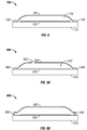
- FIG. 8 is a cross-section of a basic package structure.
- FIG. 9A is a cross-section of a package structure in accordance with an embodiment having an opening in the backplate.
- FIG. 9B is a cross-section of a package structure in accordance with an embodiment having an opening in the perimeter seal.
- FIG. 9C is a top plan view of a package structure shown in FIG. 9B .
- FIG. 9D is a top plan view of a backplate having openings according to an embodiment.
- FIG. 9E is a cross-sectional view of a package structure having openings in the backplate.
- FIG. 9F is a top plan view of a backplate having openings according to another embodiment.
- FIG. 9G is a top plan view of a backplate having openings according to yet another embodiment.
- FIG. 10 is a cross-section of a package structure in accordance with an embodiment having an opening in the backplate and desiccant within the package.
- FIGS. 11A-11B are schematic views showing a process of removing water vapor from the package according to an embodiment.
- FIG. 11C is a top plan view of the embodiment shown in FIG. 11B .
- FIG. 12 is a schematic view showing a process of removing water vapor from the package according to another embodiment.
- FIG. 13 is a schematic view showing a process of removing water vapor from the package according to still embodiment.
- FIG. 14 is a schematic view showing a process of removing water vapor from the package according to yet another embodiment.
- FIG. 15 is a schematic view showing a process of removing water vapor from the package according to yet another embodiment.
- FIGS. 16A-16C are schematic views showing a process of removing water vapor from the package according to yet another embodiment.
- FIG. 17A is a schematic view showing a process of sealing openings according to an embodiment.
- FIG. 17B is a top plan view of the embodiment shown in FIG. 17A prior to sealing the openings.
- FIG. 18 is a flow diagram illustrating one embodiment of a process for manufacturing MEMS devices, such as interferometric modulators.
- FIG. 19 is a cross-sectional view of an panel of interferometric modulator arrays having a double layered backplate.
- FIG. 20A is a flow diagram illustrating one embodiment of a process for manufacturing MEMS devices, such as interferometric modulators, wherein a groove is formed on a backplate.
- FIG. 20B is a cross-sectional view of a panel of interferometric modulator arrays having a groove formed on a backplate.
- FIG. 21 is one embodiment of a MEMS display device package, where the package has two sealant layers.
- FIG. 22 is a cross-sectional view of one embodiment of an interferometric modulator array package, wherein a plug is used to seal an orifice in a backplate.
- the embodiments may be implemented in or associated with a variety of electronic devices such as, but not limited to, mobile telephones, wireless devices, personal data assistants (PDAs), hand-held or portable computers, GPS receivers/navigators, cameras, MP3 players, camcorders, game consoles, wrist watches, clocks, calculators, television monitors, flat panel displays, computer monitors, auto displays (e.g., odometer display, etc.), cockpit controls and/or displays, display of camera views (e.g., display of a rear view camera in a vehicle), electronic photographs, electronic billboards or signs, projectors, architectural structures, packaging, and aesthetic structures (e.g., display of images on a piece of jewelry).
- MEMS devices of similar structure to those described herein can also be used in non-display applications such as in electronic switching devices.
- Embodiments of the invention relate to the packaging of MEMS devices, such as interferometric modulators by low cost, high-throughput processes.
- the MEMS devices are packaged in a process that closely mimics the manufacture of liquid crystal displays (LCDs).
- LCDs liquid crystal displays
- Large-scale manufacturing of LCDs has been undertaken by many companies throughout the world.
- adapting the packaging of MEMS devices to a process that closely parallels the LCD process allows these MEMS devices to be packaged in an efficient an high-throughput manner.
- FIG. 1 One interferometric modulator display embodiment comprising an interferometric MEMS display element is illustrated in FIG. 1 .
- the pixels are in either a bright or dark state.
- the display element In the bright (“on” or “open”) state, the display element reflects a large portion of incident visible light to a user.
- the dark (“off” or “closed”) state When in the dark (“off” or “closed”) state, the display element reflects little incident visible light to the user.
- the light reflectance properties of the “on” and “off” states may be reversed.
- MEMS pixels can be configured to reflect predominantly at selected colors, allowing for a color display in addition to black and white.
- FIG. 1 is an isometric view depicting two adjacent pixels in a series of pixels of a visual display, wherein each pixel comprises a MEMS interferometric modulator.
- an interferometric modulator display comprises a row/column array of these interferometric modulators.
- Each interferometric modulator includes a pair of reflective layers positioned at a variable and controllable distance from each other to form a resonant optical cavity with at least one variable dimension.
- one of the reflective layers may be moved between two positions. In the first position, referred to herein as the relaxed position, the movable reflective layer is positioned at a relatively large distance from a fixed partially reflective layer.
- the movable reflective layer In the second position, referred to herein as the actuated position, the movable reflective layer is positioned more closely adjacent to the partially reflective layer. Incident light that reflects from the two layers interferes constructively or destructively depending on the position of the movable reflective layer, producing either an overall reflective or non-reflective state for each pixel.
- the depicted portion of the pixel array in FIG. 1 includes two adjacent interferometric modulators 12 a and 12 b .
- a movable reflective layer 14 a is illustrated in a relaxed position at a predetermined distance from an optical stack 16 a , which includes a partially reflective layer.
- the movable reflective layer 14 b is illustrated in an actuated position adjacent to the optical stack 16 b.
- optical stack 16 typically comprise of several fused layers, which can include an electrode layer, such as indium tin oxide (ITO), a partially reflective layer, such as chromium, and a transparent dielectric.
- ITO indium tin oxide
- the optical stack 16 is thus electrically conductive, partially transparent and partially reflective, and may be fabricated, for example, by depositing one or more of the above layers onto a transparent substrate 20 .
- the partially reflective layer can be formed from a variety of materials that are partially reflective such as various metals, semiconductors, and dielectrics.
- the partially reflective layer can be formed of one or more layers of materials, and each of the layers can be formed of a single material or a combination of materials.
- the layers of the optical stack are patterned into parallel strips, and may form row electrodes in a display device as described further below.
- the movable reflective layers 14 a , 14 b may be formed as a series of parallel strips of a deposited metal layer or layers (orthogonal to the row electrodes of 16 a , 16 b ) deposited on top of posts 18 and an intervening sacrificial material deposited between the posts 18 . When the sacrificial material is etched away, the movable reflective layers 14 a , 14 b are separated from the optical stacks 16 a , 16 b by a defined gap 19 .
- a highly conductive and reflective material such as aluminum may be used for the reflective layers 14 , and these strips may form column electrodes in a display device.
- the cavity 19 remains between the movable reflective layer 14 a and optical stack 16 a , with the movable reflective layer 14 a in a mechanically relaxed state, as illustrated by the pixel 12 a in FIG. 1 .
- a potential difference is applied to a selected row and column, the capacitor formed at the intersection of the row and column electrodes at the corresponding pixel becomes charged, and electrostatic forces pull the electrodes together.
- the movable reflective layer 14 is deformed and is forced against the optical stack 16 .
- a dielectric layer within the optical stack 16 may prevent shorting and control the separation distance between layers 14 and 16 , as illustrated by pixel 12 b on the right in FIG. 1 .
- the behavior is the same regardless of the polarity of the applied potential difference. In this way, row/column actuation that can control the reflective vs. non-reflective pixel states is analogous in many ways to that used in conventional LCD and other display technologies.
- FIGS. 2 through 5B illustrate one exemplary process and system for using an array of interferometric modulators in a display application.
- FIG. 2 is a system block diagram illustrating one embodiment of an electronic device that may incorporate aspects of the invention.
- the electronic device includes a processor 21 which may be any general purpose single- or multi-chip microprocessor such as an ARM, Pentium®, Pentium II®, Pentium III®, Pentium IV®, Pentium® Pro, an 8051, a MIPS®, a Power PC®, an ALPHA®, or any special purpose microprocessor such as a digital signal processor, microcontroller, or a programmable gate array.
- the processor 21 may be configured to execute one or more software modules.
- the processor may be configured to execute one or more software applications, including a web browser, a telephone application, an email program, or any other software application.
- the processor 21 is also configured to communicate with an array driver 22 .
- the array driver 22 includes a row driver circuit 24 and a column driver circuit 26 that provide signals to a display array or panel 30 .
- the cross section of the array illustrated in FIG. 1 is shown by the lines 1 - 1 in FIG. 2 .
- the row/column actuation protocol may take advantage of a hysteresis property of these devices illustrated in FIG. 3 . It may require, for example, a 10 volt potential difference to cause a movable layer to deform from the relaxed state to the actuated state. However, when the voltage is reduced from that value, the movable layer maintains its state as the voltage drops back below 10 volts.
- the movable layer does not relax completely until the voltage drops below 2 volts.
- There is thus a range of voltage, about 3 to 7 V in the example illustrated in FIG. 3 where there exists a window of applied voltage within which the device is stable in either the relaxed or actuated state. This is referred to herein as the “hysteresis window” or “stability window.”
- hysteresis window or “stability window.”
- the row/column actuation protocol can be designed such that during row strobing, pixels in the strobed row that are to be actuated are exposed to a voltage difference of about 10 volts, and pixels that are to be relaxed are exposed to a voltage difference of close to zero volts. After the strobe, the pixels are exposed to a steady state voltage difference of about 5 volts such that they remain in whatever state the row strobe put them in. After being written, each pixel sees a potential difference within the “stability window” of 3-7 volts in this example. This feature makes the pixel design illustrated in FIG. 1 stable under the same applied voltage conditions in either an actuated or relaxed pre-existing state.
- each pixel of the interferometric modulator is essentially a capacitor formed by the fixed and moving reflective layers, this stable state can be held at a voltage within the hysteresis window with almost no power dissipation. Essentially no current flows into the pixel if the applied potential is fixed.
- a display frame may be created by asserting the set of column electrodes in accordance with the desired set of actuated pixels in the first row.
- a row pulse is then applied to the row 1 electrode, actuating the pixels corresponding to the asserted column lines.
- the asserted set of column electrodes is then changed to correspond to the desired set of actuated pixels in the second row.
- a pulse is then applied to the row 2 electrode, actuating the appropriate pixels in row 2 in accordance with the asserted column electrodes.
- the row 1 pixels are unaffected by the row 2 pulse, and remain in the state they were set to during the row 1 pulse. This may be repeated for the entire series of rows in a sequential fashion to produce the frame.
- the frames are refreshed and/or updated with new display data by continually repeating this process at some desired number of frames per second.
- protocols for driving row and column electrodes of pixel arrays to produce display frames are also well known and may be used in conjunction with the present invention.
- FIGS. 4 , 5 A, and 5 B illustrate one possible actuation protocol for creating a display frame on the 3 ⁇ 3 array of FIG. 2 .
- FIG. 4 illustrates a possible set of column and row voltage levels that may be used for pixels exhibiting the hysteresis curves of FIG. 3 .
- actuating a pixel involves setting the appropriate column to ⁇ V bias , and the appropriate row to + ⁇ V, which may correspond to ⁇ 5 volts and +5 volts respectively Relaxing the pixel is accomplished by setting the appropriate column to +V bias , and the appropriate row to the same + ⁇ V, producing a zero volt potential difference across the pixel.
- the pixels are stable in whatever state they were originally in, regardless of whether the column is at +V bias , or ⁇ V bias .
- voltages of opposite polarity than those described above can be used, e.g., actuating a pixel can involve setting the appropriate column to +V bias , and the appropriate row to ⁇ V.
- releasing the pixel is accomplished by setting the appropriate column to ⁇ V bias , and the appropriate row to the same ⁇ V, producing a zero volt potential difference across the pixel.
- FIG. 5B is a timing diagram showing a series of row and column signals applied to the 3 ⁇ 3 array of FIG. 2 which will result in the display arrangement illustrated in FIG. 5A , where actuated pixels are non-reflective.
- the pixels Prior to writing the frame illustrated in FIG. 5A , the pixels can be in any state, and in this example, all the rows are at 0 volts, and all the columns are at +5 volts. With these applied voltages, all pixels are stable in their existing actuated or relaxed states.
- pixels ( 1 , 1 ), ( 1 , 2 ), ( 2 , 2 ), ( 3 , 2 ) and ( 3 , 3 ) are actuated.
- columns 1 and 2 are set to ⁇ 5 volts
- column 3 is set to +5 volts. This does not change the state of any pixels, because all the pixels remain in the 3-7 volt stability window.
- Row 1 is then strobed with a pulse that goes from 0, up to 5 volts, and back to zero. This actuates the ( 1 , 1 ) and ( 1 , 2 ) pixels and relaxes the ( 1 , 3 ) pixel. No other pixels in the array are affected.
- row 2 is set to ⁇ 5 volts, and columns 1 and 3 are set to +5 volts.
- the same strobe applied to row 2 will then actuate pixel ( 2 , 2 ) and relax pixels ( 2 , 1 ) and ( 2 , 3 ). Again, no other pixels of the array are affected.
- Row 3 is similarly set by setting columns 2 and 3 to ⁇ 5 volts, and column 1 to +5 volts.
- the row 3 strobe sets the row 3 pixels as shown in FIG. 5A . After writing the frame, the row potentials are zero, and the column potentials can remain at either +5 or ⁇ 5 volts, and the display is then stable in the arrangement of FIG. 5A .
- FIGS. 6A and 6B are system block diagrams illustrating an embodiment of a display device 40 .
- the display device 40 can be, for example, a cellular or mobile telephone.
- the same components of display device 40 or slight variations thereof are also illustrative of various types of display devices such as televisions and portable media players.
- the display device 40 includes a housing 41 , a display 30 , an antenna 43 , a speaker 44 , an input device 48 , and a microphone 46 .
- the housing 41 is generally formed from any of a variety of manufacturing processes as are well known to those of skill in the art, including injection molding, and vacuum forming.
- the housing 41 may be made from any of a variety of materials, including but not limited to plastic, metal, glass, rubber, and ceramic, or a combination thereof.
- the housing 41 includes removable portions (not shown) that may be interchanged with other removable portions of different color, or containing different logos, pictures, or symbols.
- the display 30 of exemplary display device 40 may be any of a variety of displays, including a bi-stable display, as described herein.
- the display 30 includes a flat-panel display, such as plasma, EL, OLED, STN LCD, or TFT LCD as described above, or a non-flat-panel display, such as a CRT or other tube device, as is well known to those of skill in the art.
- the display 30 includes an interferometric modulator display, as described herein.
- the components of one embodiment of exemplary display device 40 are schematically illustrated in FIG. 6B .
- the illustrated exemplary display device 40 includes a housing 41 and can include additional components at least partially enclosed therein.
- the exemplary display device 40 includes a network interface 27 that includes an antenna 43 which is coupled to a transceiver 47 .
- the transceiver 47 is connected to a processor 21 , which is connected to conditioning hardware 52 .
- the conditioning hardware 52 may be configured to condition a signal (e.g. filter a signal).
- the conditioning hardware 52 is connected to a speaker 45 and a microphone 46 .
- the processor 21 is also connected to an input device 48 and a driver controller 29 .
- the driver controller 29 is coupled to a frame buffer 28 , and to an array driver 22 , which in turn is coupled to a display array 30 .
- a power supply 50 provides power to all components as required by the particular exemplary display device 40 design.
- the network interface 27 includes the antenna 43 and the transceiver 47 so that the exemplary display device 40 can communicate with one or more devices over a network. In one embodiment the network interface 27 may also have some processing capabilities to relieve requirements of the processor 21 .
- the antenna 43 is any antenna known to those of skill in the art for transmitting and receiving signals. In one embodiment, the antenna transmits and receives RF signals according to the IEEE 802.11 standard, including IEEE 802.11(a), (b), or (g). In another embodiment, the antenna transmits and receives RF signals according to the BLUETOOTH standard. In the case of a cellular telephone, the antenna is designed to receive CDMA, GSM, AMPS or other known signals that are used to communicate within a wireless cell phone network.
- the transceiver 47 pre-processes the signals received from the antenna 43 so that they may be received by and further manipulated by the processor 21 .
- the transceiver 47 also processes signals received from the processor 21 so that they may be transmitted from the exemplary display device 40 via the antenna 43 .
- the transceiver 47 can be replaced by a receiver.
- network interface 27 can be replaced by an image source, which can store or generate image data to be sent to the processor 21 .
- the image source can be a digital video disc (DVD) or a hard-disc drive that contains image data, or a software module that generates image data.
- Processor 21 generally controls the overall operation of the exemplary display device 40 .
- the processor 21 receives data, such as compressed image data from the network interface 27 or an image source, and processes the data into raw image data or into a format that is readily processed into raw image data.
- the processor 21 then sends the processed data to the driver controller 29 or to frame buffer 28 for storage.
- Raw data typically refers to the information that identifies the image characteristics at each location within an image. For example, such image characteristics can include color, saturation, and gray-scale level.
- the processor 21 includes a microcontroller, CPU, or logic unit to control operation of the exemplary display device 40 .
- Conditioning hardware 52 generally includes amplifiers and filters for transmitting signals to the speaker 45 , and for receiving signals from the microphone 46 .
- Conditioning hardware 52 may be discrete components within the exemplary display device 40 , or may be incorporated within the processor 21 or other components.
- the driver controller 29 takes the raw image data generated by the processor 21 either directly from the processor 21 or from the frame buffer 28 and reformats the raw image data appropriately for high speed transmission to the array driver 22 . Specifically, the driver controller 29 reformats the raw image data into a data flow having a raster-like format, such that it has a time order suitable for scanning across the display array 30 . Then the driver controller 29 sends the formatted information to the array driver 22 .
- a driver controller 29 such as a LCD controller, is often associated with the system processor 21 as a stand-alone Integrated Circuit (IC), such controllers may be implemented in many ways. They may be embedded in the processor 21 as hardware, embedded in the processor 21 as software, or fully integrated in hardware with the array driver 22 .
- the array driver 22 receives the formatted information from the driver controller 29 and reformats the data into a parallel set of waveforms that are applied many times per second to the hundreds and sometimes thousands of leads coming from the display's x-y matrix of pixels.
- driver controller 29 is a conventional display controller or a bi-stable display controller (e.g., an interferometric modulator controller).
- array driver 22 is a conventional driver or a bi-stable display driver (e.g., an interferometric modulator display).
- a driver controller 29 is integrated with the array driver 22 .
- display array 30 is a typical display array or a bi-stable display array (e.g., a display including an array of interferometric modulators).
- the input device 48 allows a user to control the operation of the exemplary display device 40 .
- input device 48 includes a keypad, such as a QWERTY keyboard or a telephone keypad, a button, a switch, a touch-sensitive screen, a pressure- or heat-sensitive membrane.
- the microphone 46 is an input device for the exemplary display device 40 . When the microphone 46 is used to input data to the device, voice commands may be provided by a user for controlling operations of the exemplary display device 40 .
- Power supply 50 can include a variety of energy storage devices as are well known in the art.
- power supply 50 is a rechargeable battery, such as a nickel-cadmium battery or a lithium ion battery.
- power supply 50 is a renewable energy source, a capacitor, or a solar cell, including a plastic solar cell, and solar-cell paint.
- power supply 50 is configured to receive power from a wall outlet.
- control programmability resides, as described above, in a driver controller which can be located in several places in the electronic display system. In some cases control programmability resides in the array driver 22 . Those of skill in the art will recognize that the above-described optimization may be implemented in any number of hardware and/or software components and in various configurations.
- FIGS. 7A-7E illustrate five different embodiments of the movable reflective layer 14 and its supporting structures.
- FIG. 7A is a cross section of the embodiment of FIG. 1 , where a strip of metal material 14 is deposited on orthogonally extending supports 18 .
- FIG. 7B the moveable reflective layer 14 is attached to supports at the corners only, on tethers 32 .
- FIG. 7C the moveable reflective layer 14 is suspended from a deformable layer 34 , which may comprise a flexible metal.
- the deformable layer 34 connects, directly or indirectly, to the substrate 20 around the perimeter of the deformable layer 34 .
- connection posts are herein referred to as support posts.
- the embodiment illustrated in FIG. 7D has support post plugs 42 upon which the deformable layer 34 rests.
- the movable reflective layer 14 remains suspended over the cavity, as in FIGS. 7A-7C , but the deformable layer 34 does not form the support posts by filling holes between the deformable layer 34 and the optical stack 16 . Rather, the support posts are formed of a planarization material, which is used to form support post plugs 42 .
- the embodiment illustrated in FIG. 7E is based on the embodiment shown in FIG. 7D , but may also be adapted to work with any of the embodiments illustrated in FIGS. 7A-7C as well as additional embodiments not shown. In the embodiment shown in FIG. 7E , an extra layer of metal or other conductive material has been used to form a bus structure 44 . This allows signal routing along the back of the interferometric modulators, eliminating a number of electrodes that may otherwise have had to be formed on the substrate 20 .
- the interferometric modulators function as direct-view devices, in which images are viewed from the front side of the transparent substrate 20 , the side opposite to that upon which the modulator is arranged.
- the reflective layer 14 optically shields the portions of the interferometric modulator on the side of the reflective layer opposite the substrate 20 , including the deformable layer 34 . This allows the shielded areas to be configured and operated upon without negatively affecting the image quality.
- Such shielding allows the bus structure 44 in FIG. 7E , which provides the ability to separate the optical properties of the modulator from the electromechanical properties of the modulator, such as addressing and the movements that result from that addressing.
- This separable modulator architecture allows the structural design and materials used for the electromechanical aspects and the optical aspects of the modulator to be selected and to function independently of each other.
- the embodiments shown in FIGS. 7C-7E have additional benefits deriving from the decoupling of the optical properties of the reflective layer 14 from its mechanical properties, which are carried out by the deformable layer 34 .
- This allows the structural design and materials used for the reflective layer 14 to be optimized with respect to the optical properties, and the structural design and materials used for the deformable layer 34 to be optimized with respect to desired mechanical properties.
- Interferometric modulators typically include moving parts, such as the movable mirrors 14 a , 14 b that must have a protected space in which to move.
- a schematic of a basic package structure 700 for an interferometric modulator is illustrated in FIG. 8 .
- a basic package structure 700 includes a transparent substrate 710 and a backplate cover or “cap” 720 .
- an interferometric modulator array 730 is encapsulated within the package structure 700 .
- the backplate 720 and transparent substrate 710 may be sealed together to protect the interferometric modulator array 730 from harmful elements in the environment.
- a method of packaging an interferometric modulator according to the embodiment shown in FIG. 8 will be discussed in more detail below.
- the packages and packaging methods described herein may be used for packaging any interferometric modulator, including, but not limited to, the interferometric modulators described above.
- the interferometric modulator array 730 is configured to reflect light through the transparent substrate and includes moving parts, such as the movable mirrors 14 a , 14 b of FIG. 1 . Therefore, to prevent these parts from being damaged, a gap or cavity 770 may be created between such moving parts and the backplate 720 . It will be understood that, in an embodiment, the gap or cavity 770 is created when a backplate 720 having a recessed area is joined to the transparent substrate 710 , as shown in FIG. 8 .
- the transparent substrate 710 may be any transparent substance capable of having thin film, MEMS devices built upon it. Such transparent substances include, but are not limited to, glass, plastic, and transparent polymers. Images are viewed through the transparent substrate 710 , which serves as an imaging surface.
- an interferometric modulator array 730 may be formed on a transparent substrate 710 . It will be understood that the fixed mirrors 16 a , 16 b (of FIG. 1 ) of the interferometric modulator array 730 are adjacent the transparent substrate 710 and the movable mirrors 14 a , 14 b are formed over the fixed mirrors 16 a , 16 b such that the movable mirrors 14 a , 14 b may move inside the package structure 700 of the embodiment shown in FIG. 8 .
- the transparent substrate 710 is covered with indium tin oxide (ITO).
- ITO indium tin oxide
- the ITO may be deposited by standard deposition techniques, including chemical vapor deposition (CVD) and sputtering, for example, to a thickness of about 500 ⁇ .
- a relatively thin layer of chrome may be deposited over the ITO.
- the ITO/chrome bilayer is then etched and patterned into columns to form the column electrodes 16 a , 16 b .
- a layer of silicon dioxide (SiO 2 ) may be formed over the ITO/chrome columns to create partially reflective fixed mirrors 16 a , 16 b .
- a sacrificial layer of, for example, silicon (Si) is deposited (and later released) over the structure to create a resonant optical cavity between the fixed mirrors 16 a , 16 b and the movable mirrors 14 a , 14 b .
- this sacrificial layer may be formed of molybdenum (Mo), tungsten (W), or titanium (Ti).
- Another mirror layer formed of aluminum, may be deposited over the sacrificial layer of silicon to form the movable mirrors 14 a , 14 b of the interferometric modulator array 730 .
- This mirror layer is deposited and patterned into rows orthogonal to the column electrodes 16 a , 16 b to create the row/column array described above.
- this mirror layer may comprise reflective metals, such as, for example, silver (Ag) or gold (Au).
- this mirror layer may be a stack of metals configured to give the proper optical and mechanical properties.
- the sacrificial layer is removed, for example, using a gas etching process, after the movable mirrors 14 a , 14 b are formed to create the optical cavity between the fixed mirrors 16 a , 16 b and the movable mirrors 14 a , 14 b .
- this sacrificial layer is removed after the backplate is joined to the transparent substrate through an opening in either the backplate or perimeter seal, as will be described in more detail below.
- Standard etching techniques may be used to remove the sacrificial layer of silicon. The particular release etching will depend on the material to be released. For example, xenon difluoride (XeF 2 ) may be used to remove the silicon sacrificial layer.
- each layer of the interferometric modulator array 730 may be deposited and patterned using standard deposition techniques and standard photolithographic techniques.
- the backplate 720 serves a mechanical function, protecting the interferometric modulator array 730 from contaminants in the environment.
- the backplate 720 along with the transparent substrate 710 and a seal 740 (which is described in more detail below) prevent mechanical interference, moisture, and contaminant gases from reaching and potentially damaging the interferometric modulator array 730 within the package 700 .
- the backplate 720 may therefore be formed of any suitable material, whether transparent or opaque, conductive or insulating.
- Suitable materials for the backplate 720 include, but are not limited to, glass (e.g., float, 1737, soda lime), plastic, ceramics, polymers, laminates, and metals and metal foils (e.g., stainless steel (SS302, SS410), Kovar, plated Kovar).
- a sealing means or a seal 740 is typically provided to join the transparent substrate 710 and the backplate 720 to form the package structure 700 .
- the seal 740 may be a semi-hermetic seal, such as a conventional epoxy-based adhesive.
- the seal 740 may be Polyisobutylene (PIB), o-rings, polyurethane, thin film metal weld, liquid spin-on glass, solders, polymers, or plastics, among other types of seals.
- the seal 740 may be a hermetic seal.
- the seal 740 may be cured and hardened.
- the seal 740 which may be hardened, between the backplate 720 and the transparent substrate 710 is different from seals that may be applied after division of the package structure 700 into individual arrays.
- the structure may be mechanically or laser scribed or otherwise prepared for division. Depending on the seal 740 , as well as other factors, it may be advantageous, after the division, to apply an endseal to the individual package structures or arrays.
- FIG. 9A A side-view illustration of an embodiment of a package structure 800 having an endseal opening is shown in FIG. 9A .
- An endseal opening is typically either an opening in an otherwise continuous perimeter seal (as shown in FIG. 9B ) or an opening or hole 850 in the backplate 820 , as shown in FIG. 9A .
- FIG. 9C is a top plan view of the embodiment shown in FIG. 9B . As shown in FIGS. 9B and 9C , the perimeter seal is not continuously dispensed, leaving an opening 860 in the seal 840 .
- openings or holes 850 in the packaging process allows packaging to take place in ambient conditions, where the atmospheric conditions are not controlled for the benefit of the manufacturing process.
- ambient conditions may be the laboratory conditions in a substantially particle-free clean room typically having a temperature around 70° F. and relative humidity in the range of about 40 to about 60%, or about 50%.
- the openings or holes 850 allow pressure within the package 800 to escape so that the pressure does not cause the transparent substrate 810 and the backplate 820 to come apart during the joining or sealing process because pressure does not build up within the package 800 . Allowing the pressure within the package to escape via the openings 850 provides for constant pressure within the package 850 , which also allows a more uniform seal width even if the seal is not dispensed with a uniform thickness.
- the opening or hole 850 may also be configured to allow material to enter and exit the package 800 .
- the opening or hole 850 may be configured to allow for application of a solvent to the interferometric modulator array 830 for removal of a spacer or sacrificial layer, which will be described in more detail below.
- a solvent to the interferometric modulator array 830 for removal of a spacer or sacrificial layer, which will be described in more detail below.
- an endseal may not be necessary, as will be described in more detail below.
- the package structure 800 may be hermetically sealed to ensure the environment within the package structure 800 remains constant regardless of the surrounding environment.
- An example of a hermetic sealing process is disclosed in U.S. Pat. No. 6,589,625, the entirety of which is hereby incorporated by reference.
- the seal 840 is a hermetic barrier that acts as an environmental barrier preventing all air and water vapor from flowing through the seal 840 and entering the package structure 800 .
- Suitable materials for a hermetic seal include, but are not limited to, welds, solders, adhesives mixed with molecular sieves, such as a zeolite.
- the adhesive component alone cannot act as a suitable environmental barrier because it will eventually allow moisture and other contaminants to permeate into the package structure 800 .
- a semi-hermetic seal 840 of one of the aforementioned materials is desirable for space-critical environments because the seal 840 can be very thin and inexpensive, relative to other sealing techniques, such as welding and soldering.
- the semi-hermetic seal 840 may be applied through simple in-line manufacturing processes, whereas the techniques of welding and soldering for hermetic seals require very high temperature processes that can damage the package structure 800 , are relatively expensive, and tend to occupy much more space because a welded or soldered seal is thicker. It will be understood that a semi-hermetic seal may include an adhesive that is not mixed with any molecular sieves or desiccants.
- the zeolites may include aluminosilicate-structured minerals, such as sodium aluminosilicate. In another embodiment, the zeolites may include microporous silicate-structured minerals. It will be appreciated that active components, other than zeolites, that can act as absorbing filters on the molecular level can also be used.
- the adhesives may be a low outgassing adhesive. In other embodiments, the adhesives may be adhesives with varied outgassing.
- a desiccant used in the seal may be a calcium dioxide, strontium oxide (SRO), silica gels, montmorillonite clay (such as a magnesium aluminum silicate), molecular sieves (zeolites), or calcium sulfates.
- the amount of material for the seal 840 will depend on the estimated amount of moisture or contaminant gases that will need to be removed from within the package structure 800 during the lifetime of the package structure 800 .
- the amount of material for the seal 840 also depends not only on the amount of moisture or contaminant gases inside the package structure 800 when the package is formed, but also the permeation rate of the seal 800 and the outgassing potential of the package components.
- Zeolites may absorb water molecules at relatively high temperatures. Zeolites can trap moisture and contaminant gases in their pores. The skilled artisan will understand that zeolites having deferent pore sizes can be selected for the seal 840 material to absorb different contaminants. In an embodiment, zeolites are selected to absorb contaminant molecules, such as aromatic branched-chain hydrocarbons that have critical diameters of up to ten angstroms. In another embodiment, zeolites having pore sizes between two and three angstroms may be selected to abort contaminant molecules having diameters of less than two angstroms, such as hydrogen and moisture molecules. In still another embodiment, zeolites having pore sizes of about fifty angstroms (50 ⁇ ) can be used to absorb nitrogen and carbon dioxide molecules. The skilled artisan will appreciate that the hermetic seal 840 may be comprised of a mixture of zeolites having various pore sizes.
- the seal 840 is typically applied to the transparent substrate 810 along the perimeter, around the interferometric modulator array 830 .
- the seal 840 is typically applied to the transparent substrate 810 around the perimeter of the of interferometric modulator array 830 .
- the seal 840 may be formed to a thickness in a range of about 1 to about 20 microns, or in a range of about 12 to about 18 microns, or about 15 microns.
- the thickness of the seal 840 will depend on various factors, including the estimated lifetime of the device, the material of the seal 840 , the amount of contaminants and moisture that are estimated to permeate into the package structure 800 during the lifetime, the humidity of the ambient environment, and whether a desiccant is included within the package structure 800 and the flatness of the backplate 820 and the transparent substrate 810 .
- the backplate 820 is then positioned over the transparent substrate 810 , and the transparent substrate 810 and the backplate 820 are sealed together by the seal 840 to form the package structure 800 .
- an outer bead (not shown) of adhesive is applied around the perimeter of the seal 840 .
- the outer bead may include a low permeation rate adhesive, which can provide additional environmental protection to the package structure 800 .
- the outer bead of adhesive may be useful in an environment having a great deal of contaminants where the seal 840 alone cannot serve as an effective hermetic seal without being loaded with an impractical amount of the active component. For example, if the seal 840 includes a high portion of zeolites (e.g., more than 60 percent zeolites by weight), the seal 840 can become microscopically porous as well as highly viscous and thus difficult to apply. Such a seal 840 having a high portion of zeolites may not provide a robust mechanical support to the package structure 800 .
- the outer bead may also provide additional mechanical support.
- the backplate 820 may be formed with at least one opening 850 therein.
- a release material such as xenon difluoride (XeF 2 ) may be introduced through the opening into the interior of the package structure 800 to remove the sacrificial layer within the interferometric modulator array 830 (between the fixed mirrors 16 a , 16 b and the movable mirrors 14 a , 14 b ).
- the number and size of these openings 850 may depend on the desired rate of removal of the sacrificial layer.
- xenon difluoride may be introduced into the interior of the package structure 800 through an opening or openings 850 in the backplate 820 .
- Such openings 850 in the backplate 820 may be created by etching an opening in the backplate 820 .
- the xenon difluoride (XeF 2 ) reacts with the sacrificial layer to remove it.
- a sacrificial layer formed of spin-on glass or oxide may be gas etched or vapor phase etched to remove the sacrificial layer after the backplate 820 has been joined to the transparent substrate 810 .
- the removal process will depend on the material of the sacrificial layer.
- the opening(s) 850 in the backplate 820 may be sealed.
- a thermally or UV cured polymer is used to seal these openings.
- the opening(s) may also be sealed with metal or glass caps, metal foil, adhesive, welds, or solder. The skilled artisan will appreciate that other materials may be used as well and that materials having high viscosity are advantageous.
- the package structure 800 may have an opening 860 in the perimeter seal 840 rather than, or in addition to, an opening in the backplate 820 .
- the opening 860 in the seal 840 provides the same advantages as those described above for an opening in the backplate 820 , including allowing for packaging at ambient conditions, and introduction of a release material, desiccant, and self-aligning monolayer.
- the opening 860 in the seal 840 may be closed to form a sealed opening after the joining of the transparent substrate 810 and the backplate 820 and introduction of desiccant, release material, and self-aligning monolayer, if desired.
- the opening 860 is sealed with a polymer, such as UV or thermally cured. It is advantageous that the polymer has a lower viscosity than that of the perimeter seal 840 such that increase surface tension helps the polymer to fully seal the opening 860 .
- the opening or hole 850 may be closed to form an endseal or sealed opening to complete the package 800 with, for example, a metal or glass cap, metal foil, adhesive, solder, or UV or thermally cured polymer.
- metal caps may be used with a backplate formed of a printed circuit board (PCB) backplate that may include electronic interfaces for use with radio-frequency (RF) signals.
- PCB backplate may serve not only as protection for circuitry that is integrated into the backplate but may also enhance RF circuit needs.
- metal caps may be included for RF enhancement or protection.
- Antenna properties may also be incorporated into the PCB backplate or the interferometric modulator, including, but not limited to, the use of a metal backplate or a metal cap as an antenna for a cellular phone.
- a desiccant can be applied inside the package structure 800 in a vapor form through, for example, the opening(s) 850 .
- a portion of a desiccant 860 could be included or applied to the interior surface of the backplate 820 , as shown in FIG. 9 .
- more or other types of desiccants can be applied to the interior of the package 800 through the opening(s) 850 .
- the size of the opening(s) 850 may be small and can thereby allow both high-absorption rate desiccant or slow-absorption rate desiccant to be incorporated into the backplate 820 prior to joining of the backplate 820 to the transparent substrate 810 because the amount of air that will pass into the package 800 through the opening(s) without any vacuum or pressure driving force is sufficiently small.
- the opening 850 has a diameter in a range of about 10 to about 100 microns.
- the opening(s) 850 allow for a desiccant 860 to be incorporated into the backplate 820 prior to assembly and for some gas or etchant to be injected through the opening(s) 850 to either activate the desiccant 860 or to deposit additional desiccant in the package 800 .
- a desiccant may be used to control moisture resident within the package structure 800 .
- a desiccant may not be necessary to prevent moisture from traveling from the atmosphere into the interior of the package structure 800 .
- a desiccant may be advantageous.
- the lifetime expectation of the device may depend on the lifetime of the desiccant.
- the interferometric modulator display may fail as sufficient moisture enters the package structure to cause damage to the interferometric modulator.
- the theoretical maximum lifetime of the device is determined by the water vapor flux into the package as well as the amount and type of desiccant.
- the lifetime of the device is not dependent on the desiccant capacity, or the geometry of the seal.
- the interferometric modulator will not fail due to a consumed desiccant.
- a desiccant may be used to reduce moisture resident within the package structure 800 .
- Desiccants may be used for packages that have either hermetic or semi-hermetic seals.
- a desiccant may be used to control moisture moving into the package from the environment.
- a desiccant may not be necessary for a hermetically sealed package, but may be desirable to control moisture within the package structure 800 .
- desiccants may be provided within the package to absorb any moisture that moves into the package during the manufacturing process.
- any substance that can trap moisture while not interfering with the optical properties of the interferometric modulator array 830 may be used as the desiccant.
- Suitable desiccant materials include, but are not limited to, zeolites, molecular sieves, surface adsorbents, bulk adsorbents, and chemical reactants. The skilled artisan will appreciate that the desiccant material should be selected based on a variety of factors, including the estimated amount to contaminant gases in the environment as well as the absorption rate and amount of the desiccant material.
- the desiccant may be in different forms, shapes, and sizes.
- the desiccant may alternatively be in powder form. These powders may be inserted directly into the package or they may be mixed with an adhesive for application.
- the desiccant may be formed into different shapes, such as cylinders or sheets, before being applied inside the package.
- the desiccant may be applied after the transparent substrate 810 and the backplate 820 are joined.
- a small hole or opening 850 is formed in the backplate 820 .
- the opening or hole 850 may be formed prior to joining the backplate 820 to the transparent substrate 810 .
- the opening or hole 850 allows desiccant 865 to be injected into individual package structures 800 after the backplate 820 and transparent substrate 810 have been sealed together.
- sealing the opening or hole 850 is also required to form the sealed package structure 800 such that the interior of the package structure 800 is isolated from the surrounding ambient environment.
- the skilled artisan will appreciate that the opening or hole 850 can also facilitate a complete perimeter seal process, thereby eliminating the typical LCD-type endseal opening used in the perimeter seal 840 .
- the opening or hole 850 in the backplate 820 may be sealed after injection of a desiccant into the package 800 .
- a self-aligning monolayer is applied within the package 800 to allow the moving parts (e.g., elements 14 a , 14 b ) of the interferometric modulator array 830 to move easily.
- the self-aligning monolayer can be applied to the interior of the package structure 800 through the opening(s) 850 .
- the monolayer may comprise a material configured to reduce the surface friction on the moving parts and/or repel water vapor from the moving parts.
- Exemplary materials for the self-aligning monolayer include, but are not limited to, fluoro silane, chloro-fluoro silane, methoxy silane, trichlorosilane, perfluorodecanoic carboxylic acid, octadecyltrichlorosilane (OTS), dichlorodimethylsilane, or hydrophobic or non-stick materials, such as PTFE, teflon, silicone, polystyrene, polyurethane (both standard and ultraviolet curable), a block copolymer containing a hydrophobic component (for example poly-methyl-methacrylate), or polysilazane (especially with polisiloxane).
- fluoro silane fluoro silane
- chloro-fluoro silane methoxy silane
- trichlorosilane perfluorodecanoic carboxylic acid
- OTS octadecyltrichlorosilane
- an exemplary materials for a self-aligning monolayer include, but are not limited to, inorganic materials such as one or more of the following: graphite, diamond-like carbon (DLC), silicon carbide (SiC), a hydrogenated diamond coating, or fluorinated DLC.
- inorganic materials such as one or more of the following: graphite, diamond-like carbon (DLC), silicon carbide (SiC), a hydrogenated diamond coating, or fluorinated DLC.
- interferometric modulators have a higher tolerance (e.g., up to about 10%) for humidity requirements that organic light emitting diodes (OLED) displays. It is possible that water vapor permeates into the package 800 even if it is semi-hermetically or hermetically sealed. In certain embodiments in which a desiccant is placed in the interior of the package 800 , a certain amount of moisture permeation may be tolerated, depending on the capacity of the desiccant. However, if there exists moisture or water vapor in an amount higher than the tolerance level, or if there is more water permeation into the package 800 than desired, the interferometric modulator array 830 is likely to have a shortened lifetime or may fail to operate properly.
- OLED organic light emitting diodes
- moisture which has been created and/or permeated during assembly, may not have been properly removed before completing the fabrication of the package.
- the relative humidity level in the interior of the package, particularly without a desiccant should be maintained less than the tolerance level so that the interferometric modulator array 830 operates properly for the duration of its expected lifetime.
- FIGS. 11A-11B illustrate schematic diagrams showing a process of removing water vapor from the package according to an embodiment.
- the package 900 in FIG. 11A includes a desiccant 970 , whereas the package 900 in FIG. 11B does not.
- FIG. 11C is a top plan view of the embodiment shown in FIG. 11B .
- the seal 940 is not dispensed continuously to create an inlet 960 and an outlet 980 in the seal 940 .
- a water vapor removing process will be described in more detail below.
- the term “water vapor” may include any kind of water, including, but not limited to, liquid water, gaseous water (in vapor phase), or condensed water on surfaces inside the package.
- an inlet 960 and an outlet 980 are defined in the seal 940 .
- the inlet 960 is configured to supply a gas into the interior of the package 900 and the outlet 980 is configured to allow water vapor to exit the package 900 .
- one inlet and one outlet are defined in the seal 940 .
- one inlet and a plurality of outlets are defined in the seal.
- at least one of the inlet 960 and outlet 980 is formed with the use of a scriber.
- the shape of the inlet 960 and outlet 980 is substantially circular.
- the inlet 960 and outlet 980 may have shapes other than circular. The skilled artisan will appreciate that the inlet 960 and/or outlet 980 may alternatively be formed by drilling or with the use of any other appropriate tool or process.
- the inlet 960 and the outlet 980 have substantially the same size. In other embodiments, the inlet 960 and outlet 980 may be of different sizes. For example, the size of the inlet 960 can be greater than that of the outlet hole 980 . Alternatively, the sizes of the inlet 960 and outlet 980 may be determined by the criteria of how effectively or easily they may be sealed after the water vapor is removed, as will be described in more detail below. In other words, so long as sealing can be effectively performed, the inlet 960 and outlet 980 can be of any size. The diameter of at least one of the inlet 960 and the outlet 980 may be in the range of about 10 microns to about 2 mm, or in the range of about 500 microns to about 1.5 mm, or about 1 mm.
- the inlet 960 and outlet 980 may be defined in the seal 940 simultaneously. Alternatively, one of the inlet 960 and the outlet 980 is defined first and thereafter the other is defined in the seal 940 .
- the inlet 960 may be formed first, and the outlet 980 may be formed after gas has been introduced through the inlet 960 and into the package 900 .
- the gas pressure in the interior of the package 900 can be increased so as to enhance the water vapor removal process.
- the gas introduced into the package 900 is a dry inert gas, such as molecular nitrogen, N 2 .
- the gas is argon.
- the gas can be any type of gas that is effective in removing water vapor in the interior of the package 900 by, for example, pressure, drying, driving off (blowing), or vacuuming (sucking).
- the gas may be, for example, air, heated air, a heated gas, or a dry gas.
- the gas may be continuously fed through the inlet 960 and into the interior of the package 900 until all of the water vapor is substantially removed.
- whether the water vapor has been substantially removed can be determined by monitoring the humidity at the outlet port 980 to measure the humidity of the gas exiting the outlet 980 .
- the package 900 can be placed in a chamber (or vacuum chamber), and the gas may be fed into the package 900 by evacuating the chamber and then refilling it with a dry gas, such as nitrogen or argon.
- a dry gas such as nitrogen or argon.
- at least a partial vacuum is created around the package 900 to draw out the water vapor from the interior of the package 900 . It will be understood that, in this embodiment, only one opening in the package 900 is necessary. Thus, it is not necessary to have both an inlet 960 and an outlet 980 is this embodiment.
- water vapor may be removed during the fabrication process for the package 900 .
- a “release” or removal process can be used in which the sacrificial layer in the interferometric modulator array 930 is etched away first, as described above. Then, water vapor (and/or any unwanted or unnecessary material) in the interior of the package 900 can be removed with the use of a carrier gas (e.g., nitrogen or argon) introduced into the package through the inlet 960 formed in the seal 940 .
- a carrier gas e.g., nitrogen or argon
- the removal process is performed by a MEMS etching system, such as, for example, X3 Series Xetch, which is available from XACIX, USA, and MEMS ETCHER, which is available from Penta Vacuum, Singapore.
- a MEMS etching system such as, for example, X3 Series Xetch, which is available from XACIX, USA, and MEMS ETCHER, which is available from Penta Vacuum, Singapore.
- FIG. 12 is a schematic diagram showing a process of removing water vapor from the interior of the package according to another embodiment.
- a thin film 1020 is instead deposited over the transparent substrate 1010 and a sacrificial layer formed over the interferometric modulator array 1030 .
- the inlet 1040 and outlet 1050 are formed in the thin film Backplate 1020 , as shown in FIG. 12 . It will be understood that the sacrificial layer needs to be removed to create a cavity below the Backplate 1020 .
- a release material such as xenon difluoride (XeF 2 ) may be introduced through an opening 1040 , 1050 in the thin film 1020 into the interior of the package structure 1000 to remove the sacrificial layer.
- XeF 2 xenon difluoride
- the water vapor inside the package may be removed using the methods described above.
- a package structure having a thin film backplate is described in U.S. patent application Ser. No. 11/045,738, filed Jan. 28, 2005, which is hereby incorporated herein in its entirety.
- FIG. 13 is a schematic diagram showing a process of removing water vapor from a package 1100 according to another embodiment.
- an inlet 1150 is formed in the backplate 1120 rather than in the seal 1140 .
- the backplate 1120 is formed of a material, such as glass, metal, or flexible polymer, the inlet 1150 can be effectively created in the backplate 1120 with the use of a scriber or laser, for example.
- An outlet 1160 may be formed in the seal 1140 by dispensing a non-continuous seal, as shown in FIG. 13 . Gas may be fed into the package 1100 through the inlet 1150 to remove water vapor and/or unwanted material. Alternatively, it will be understood that the inlet may be formed in the seal and the outlet may be formed in the backplate.
- FIG. 14 is a schematic diagram showing a package configuration for removing water vapor from a package 1200 according to another embodiment.
- both the inlet 1250 and the outlet 1260 are formed in the backplate 1220 and not in the seal 1240 , as shown in FIG. 13 .
- gas may be fed into the package 1200 to remove water vapor and/or unwanted material.
- the inlet 1250 and outlet 1260 maybe be formed in the backplate 1220 during the fabrication process for the backplate 1220 .
- FIG. 15 is a schematic diagram showing a package configuration for removing water vapor from a package 1300 according to yet another embodiment.
- an inlet 1350 is formed in the transparent substrate 1310 and the outlet 1360 is formed in the seal 1340 by dispensing a non-continuous seal, as shown in FIG. 15 .
- the transparent substrate 1310 is formed of a material, such as, for example, glass, plastic, or polymer
- the inlet 1350 can be effectively defined in the transparent substrate 1310 with the use of a scriber or a laser, for example.
- gas may be introduced into the package 1300 to remove water vapor from the interior of the package.
- FIGS. 16A-16C are schematic diagrams showing a process of removing water vapor from a package 1400 according to another embodiment.
- the opening 1450 may be formed in the seal 1440 .
- the opening 1460 may be formed in the backplate 1420 .
- the opening 1470 may be formed in the transparent substrate 1410 .
- heated air or a heated gas may be introduced into the package 1400 to dry the water vapor within the package 1400 .
- vacuuming may also be performed to draw out any remaining water vapor from the interior of the package 1400 .
- the opening 1450 , 1460 , 1470 can also be used to inject desiccant, a release material, or self-aligning monolayer, as described in detail above.
- FIGS. 17A and 17B are cross-sectional and top view diagrams, respectively, showing sealing openings 1550 in a package 1500 , according to an embodiment.
- openings 1550 may be sealed to form an endseal.
- the openings 1550 in the seal are formed by dispensing a non-continuous seal 1540 .
- openings 1550 in the seal 1540 are sealed with the same material that forms the perimeter seal 1540 . It will be understood that although FIG. 17A shows a sealing process for a package having openings in the seal 1540 , the same or a similar sealing process can be performed for other embodiments.
- openings in a backplate may be sealed with the same material that forms the backplate.
- openings in a transparent substrate may be sealed with the same material that forms the transparent substrate.
- the openings may be sealed with alternative materials, including, but not limited to, thermally or UV cured epoxies, having a low viscosity, welds, solders, metal caps, and glass caps.
- the packaging process including an endseal process, may be accomplished in a vacuum, pressure between a vacuum up to and including ambient pressure, or pressure higher than ambient pressure.
- the packaging process may also be accomplished in an environment of varied and controlled high or low pressure during the sealing process.
- the packaging environment may be of an inert gas at ambient conditions.
- Packaging at ambient conditions allows for a lower cost process because it provides more potential for versatility in equipment choice and because the device may be transported through ambient conditions without affecting the operation of the device.
- a front glass plate and a rear glass plate are sandwiched together to create an LCD display.
- the front glass plate and the rear glass plate are produced in different production lines.
- the two glass plates are aligned, combined and fixed together, normally using thermally curable epoxy.
- the glass panels are pressed together and heated in order to cure the seals and create a stable panel structure.
- the glass panels are then scribed and broken to the final display dimensions.
- a single set of front and rear glass plates can be used to produce several individual display panels by scribing and breaking the plates once they are sealed together.
- An opening in the seal is provided so the two plates can be brought in close proximity without a resultant build-up of internal air pressure within the interior of the plate sandwich.
- the opening provides a way to introduce the liquid crystal material between the glass plates.
- the edges are ground and the singularized displays are filled with liquid crystal liquid and the opening in the seal is then closed using UV curable polymer.
- this type or another similar type of process can be advantageously adapted to the packaging of other types of display products, such as interferometric modulator displays.
- a first glass plate having a set of interferometric modulator arrays can be provided.
- a thermally curable or UV curable polymer material can be screen printed around the outer circumference of each array.
- a second glass plate can then be pressed against the first glass plate and heated to cure the seal between each array.
- the arrays can then be scribed and broken apart into individual display components.
- Some embodiments include a variety of methods for overcoming the problems associated with air pressure building up between the glass plates as they are sandwiched together.
- the thermally curable or UV curable polymer can be printed in around each array, however a small gap can be left to provide an air passage between the interior of the array and the external environment. After the glass plates have been sealed together, the gap can thereafter be sealed to protect the interior of the array from the external environment using, for example, a UV curable polymer, similar to LCD packaging.
- a UV curable polymer similar to LCD packaging.
- water vapor in the air can cause mirrors within the modulator array to stick and not function properly.
- sealing the small gap left in the polymer will prevent ambient water vapor from entering the interior of the modulator array.
- a desiccant is introduced between the glass plates, in a method similar to introduction of the liquid crystal solution between glass panels in an LCD display. If a gap is left open from the external environment to the interior of each modulator array, a low-viscosity liquid polymer with incorporated desiccant can be introduced between the glass panels and allowed to flow inside of each modular array.
- the low viscosity liquid polymer with desiccant can comprise any of the desiccants described above, including calcium oxide, strontium oxide (SrO), silica gels, montmorillonite clay (e.g. a magnesium aluminum silicate), molecular sieves (zeolites), calcium sulfates, or a combination thereof.
- the low-viscosity liquid desiccant comprises a UV curable epoxy filled with desiccant material.
- a series of orifices can be provided in either glass plate so that the air pressure does not build up inside the devices as the glass plates are brought together to form the package.
- the first glass plate may provide the interferometric modulator arrays and the thermally curable or UV curable polymer circumscribing each array.
- the second glass plate may include a series of small orifices configured to be positioned opposite each array as the two glass plates are sandwiched together. Once the plates are sandwiched together to form a package, the orifices in the second glass plate can be sealed by a method, such as is described above. After the thermally curable or UV-curable polymer has hardened, the arrays can be separated, for example, by scribing and braking apart to provide individual modulator arrays.
- FIG. 18 One embodiment of a process 1800 for manufacturing a MEMS device is shown in FIG. 18 .
- a first backplate 1810 is provided with a series of orifices 1820 A-D.
- the first backplate may be, for example, approximately 0.3 mm thick.
- a resin 1830 A-D is applied through silk screening, inkjet, or another technology, to circumscribe each orifice 1820 A-D.
- the resin is approximately 4-12 ⁇ m in height and 0.7-1 mm in width.
- the resin 1830 A-D is configured so that when the first backplate 1810 is sealed to the iMoD array plate 1840 , the resin provides an airtight seal around the outer periphery of each modulator array 1842 A-D.
- the resin is a UV-curable sealant.
- the resin is thermal glue that is cured by baking the glass plates.
- the thermal glue may be an acrylic epoxy type which is baked in an oven at, for example, approximately 160° C. to be cured.
- the first backplate comprises a series of orifices 1820 A-D, there would be no air pressure built up when the two plates are brought together. Any air pressure that would normally be built up between the plates would escape through the orifices 1820 A-D into the ambient environment.
- a second backplate 1850 is sealed to the first Backplate 1810 .
- the second backplate 1850 may be, for example, approximately 0.4 mm thick.
- the combination of the first and the second backplates creates a dual-backplate structure of, for example, approximately 0.7 mm in thickness.
- the second backplate 1850 contains desiccant areas 1852 A-D which are configured to align with the orifices 1820 A-D in the first backplate.
- the desiccant areas 1852 A-D are adjacent the interferometric modulators 1842 A-D. The position of these components with respect to one another will be described in more detail with reference to cross-sectional FIG. 19 .
- the final three-layered display panel is scribed and broken into individual display cells for further processing.
- the iMoD array plate 1840 may contain either released or unreleased interferometric modulators. If the interferometric modulators are not released, then a release gas may be used to release the iMoDs 1842 A-D after they iMoD array plate 1840 has been sealed to the first backplate 1810 . Because the first backplate 1810 includes orifices 1820 A-D, the release gas can contact the individual arrays 1842 A-D even after the sandwich between the plates 1810 and 1840 has been created. This provides an advantage in that the thermal processing required to seal the plates 1810 and 1840 together may be harmful to unreleased components. Accordingly, using this process, the interferometric modulators may remain unreleased until after the thermal bonding step has been completed.
- the size and pattern of the desiccant illustrated in FIG. 18 is not limiting on the invention. Desiccant areas of virtually any size or shape that help absorb moisture from the interior of the interferometric modulator array are anticipated to work similarly.
- FIG. 19 shows a cross sectional view of the triple layer sandwich created by the plates 1840 , 1810 and 1850 .
- the lower plate 1840 includes the interferometric modulator arrays 1842 A-D. Opposite the arrays 1842 A-D are orifices 1820 A-D, and exposed through the orifices are desiccant areas 1852 A-D from the second backplate 1850 .
- the resin 1830 A-D seals each modulator array 1842 A-D from each other array. In one embodiment, the resin provides a fully hermetic seal between the arrays.
- the first backplate 1810 and the second backplate 1850 are sealed together prior to contacting the iMoD array plate 1840 .
- a small opening is left in the resin layer 1820 A-D in order to prevent air pressure from building up when the two backplate layers are sealed to the array plate 1840 .
- the openings in the resin layer 1820 A-D can be sealed with additional resin or adhesive.
- a backplate 2010 having a series of grooves 2012 A-D.
- the grooves 2012 A-D are in a square configuration.
- the grooves can be created by, for example, mechanical scribing or chemical etching or sandblasting a channel in the backplate 2010 in the desired pattern.
- a series of resin patterns 2020 A-D are then applied along the outer circumference of the grooves 2012 A-D.
- a small opening 2022 A is left in each of the resin patterns to allow air to flow out from the device as it is packaged.
- An iMoD array plate 2025 having a set of interferometric modulator arrays 2030 A-D is then aligned and adhered to the backplate 2010 to form a package by curing the resin 2020 A-D in a manner similar to that described in the process of FIG. 18 .
- each iMoD array 2030 A-D is aligned opposite each of the respective grooves 2012 A-D.
- the resin layer 2020 A-D seals each modulator array 2030 A-D from the external environment, with the exception of a small opening.
- a liquid desiccant can be, for example, a very low viscosity UV epoxy mixed with calcium oxide powder (CaO). This liquid desiccant can then be flowed into each array package through the small opening 2022 A in the resin 2020 A-D.
- the sandwich formed by the plates 2010 and 2025 is scribed and broken into individual array panels 2050 prior to addition of the liquid desiccant.
- the grooves 2012 A-D will also fill with desiccant to provide a fairly thick circumference of desiccant just on the interior edge of the resin layer.
- the small opening in the resin layer can then be sealed to prevent the desiccant from flowing back out of the array package.
- a UV epoxy filled with desiccant can be UV cured to lock-in the desiccant in place. This also would prevent the ambient environment from entering the interior of the array package.
- the modulator array plate 2025 includes a series of interferometric modulators 2030 A-D which are disposed opposite the backplate 2010 .
- the backplate 2010 has a series of grooves 2012 A-D which are carved into the backplate 2010 .
- a resin layer 2020 A-D separates each modulator array from the other arrays.
- the backplate 2010 may be layered with two or more layers of resin.
- an inner layer of resin 2105 on the interior of groove 2112 may be provided.
- an outer resin layer 2110 may be provided on the exterior of the groove 2112 .
- the inner layer of resin 2105 may have very small air permeable openings 2120 that would allow escape of increasing air pressure, but would not allow a liquid desiccant to flow into the inner portion of the modulator array package.
- the liquid desiccant is flowed through an opening 2125 in the outer layer of resin 2110 it will fill the groove 2112 , but not flow over the actual modulator array. This would prevent the modulator array from being damaged by the liquid desiccant or any byproducts of the desiccant.
- FIG. 22 shows another embodiment of a MEMS device 2200 that can be made by a LCD compatible process.
- a first plate 2210 having an interferometric modulator array 2212 is shown.
- the substrate is sealed to a backplate 2215 by sealants 2220 A and 2220 B.
- the backplate 2215 contains a tapered orifice 2225 which can be used to allow air to escape while the two plates 2210 and 2215 are brought together and sealed.
- a tapered plug 2230 having a desiccant tip 2235 is used to fill the orifice 2225 once the plates 2210 and 2215 are sealed together.
- the tapered plug can be a small piece of glass, or other material such as metal or ceramic. In practice the tapered plug would be glued into place using an epoxy or other sealant as described above.
- the process of making the device 2200 can start from a plate of several arrays, as described in FIG. 18 . At the end of that process, the individual arrays can be scribed and separated from the other arrays on the plate.
- a MEMS package 2300 is formed using four glass spacers 2310 A-D.
- the spacers 2310 A-D fit together to form a frame around an interferometric modulator array 2325 .
- An epoxy bond 2330 holds the four spacers 2310 A-D together in the frame configuration.
- the epoxy bond 2330 may, for example, be a thermally curable or UV curable epoxy.
- the frame has four corners 2333 A-D which provide an air permeable passageway between the spacers from the ambient environment to the interior of a package formed around the modulator array 2325 .
- the four glass spacers 2310 A-D bond to a transparent substrate 2350 .
- the transparent substrate 2350 supports the interferometric modulator array 2325 .
- the spacers support a glass backplate 2355 which includes a desiccant 2360 .
- the corners 2333 A-D initially function as crevices for excessive air pressure when the backplate 2355 with desiccant 2360 is attached.
- the edge crevices prevent air pressure from building up within the package during the step of joining the transparent substrate 2350 to the backplate 2355 . Later the edge crevices between the spacers can be sealed by a resin.
Landscapes
- Physics & Mathematics (AREA)
- Engineering & Computer Science (AREA)
- General Physics & Mathematics (AREA)
- Optics & Photonics (AREA)
- Microelectronics & Electronic Packaging (AREA)
- Manufacturing & Machinery (AREA)
- Spectroscopy & Molecular Physics (AREA)
- Mechanical Light Control Or Optical Switches (AREA)
- Laminated Bodies (AREA)
- Packaging Frangible Articles (AREA)
Abstract
Description
Claims (25)
Priority Applications (1)
| Application Number | Priority Date | Filing Date | Title |
|---|---|---|---|
| US11/734,730 US7746537B2 (en) | 2006-04-13 | 2007-04-12 | MEMS devices and processes for packaging such devices |
Applications Claiming Priority (2)
| Application Number | Priority Date | Filing Date | Title |
|---|---|---|---|
| US79173006P | 2006-04-13 | 2006-04-13 | |
| US11/734,730 US7746537B2 (en) | 2006-04-13 | 2007-04-12 | MEMS devices and processes for packaging such devices |
Publications (2)
| Publication Number | Publication Date |
|---|---|
| US20070242341A1 US20070242341A1 (en) | 2007-10-18 |
| US7746537B2 true US7746537B2 (en) | 2010-06-29 |
Family
ID=38562921
Family Applications (2)
| Application Number | Title | Priority Date | Filing Date |
|---|---|---|---|
| US11/734,730 Expired - Fee Related US7746537B2 (en) | 2006-04-13 | 2007-04-12 | MEMS devices and processes for packaging such devices |
| US11/735,362 Expired - Fee Related US7715080B2 (en) | 2006-04-13 | 2007-04-13 | Packaging a MEMS device using a frame |
Family Applications After (1)
| Application Number | Title | Priority Date | Filing Date |
|---|---|---|---|
| US11/735,362 Expired - Fee Related US7715080B2 (en) | 2006-04-13 | 2007-04-13 | Packaging a MEMS device using a frame |
Country Status (3)
| Country | Link |
|---|---|
| US (2) | US7746537B2 (en) |
| EP (1) | EP1979268A2 (en) |
| WO (2) | WO2007120885A2 (en) |
Cited By (14)
| Publication number | Priority date | Publication date | Assignee | Title |
|---|---|---|---|---|
| US20090068795A1 (en) * | 2002-12-27 | 2009-03-12 | Shinko Electric Industries Co., Ltd. | Production methods of electronic devices |
| US7816164B2 (en) | 2006-12-01 | 2010-10-19 | Qualcomm Mems Technologies, Inc. | MEMS processing |
| US20110012219A1 (en) * | 2007-09-28 | 2011-01-20 | Qualcomm Mems Technologies, Inc. | Optimization of desiccant usage in a mems package |
| US7978396B2 (en) | 2003-08-15 | 2011-07-12 | Qualcomm Mems Technologies, Inc. | Optical interference display panel |
| US8004736B2 (en) | 2003-08-18 | 2011-08-23 | Qualcomm Mems Technologies, Inc. | Optical interference display panel and manufacturing method thereof |
| US8040587B2 (en) | 2006-05-17 | 2011-10-18 | Qualcomm Mems Technologies, Inc. | Desiccant in a MEMS device |
| US20120025363A1 (en) * | 2010-08-02 | 2012-02-02 | Advanced Semiconductor Engineering, Inc. | Package structure and manufacturing method thereof |
| CN102344109A (en) * | 2010-08-02 | 2012-02-08 | 日月光半导体制造股份有限公司 | Packaging structure and manufacturing method thereof |
| US20120099179A1 (en) * | 2004-09-27 | 2012-04-26 | Qualcomm Mems Technologies, Inc. | Method and device for providing electronic circuitry on a backplate |
| US8379392B2 (en) | 2009-10-23 | 2013-02-19 | Qualcomm Mems Technologies, Inc. | Light-based sealing and device packaging |
| US8410690B2 (en) | 2009-02-13 | 2013-04-02 | Qualcomm Mems Technologies, Inc. | Display device with desiccant |
| US8760797B1 (en) | 2013-06-13 | 2014-06-24 | Seagate Technology Llc | Contamination control for a disc drive |
| US8921956B2 (en) | 2013-01-25 | 2014-12-30 | Infineon Technologies Ag | MEMS device having a back plate with elongated protrusions |
| US20150014798A1 (en) * | 2013-07-15 | 2015-01-15 | Stmicroelectronics S.R.L. | Assembly for a mems environmental sensor device having improved resistance, and corresponding manufacturing process |
Families Citing this family (38)
| Publication number | Priority date | Publication date | Assignee | Title |
|---|---|---|---|---|
| US8124434B2 (en) * | 2004-09-27 | 2012-02-28 | Qualcomm Mems Technologies, Inc. | Method and system for packaging a display |
| US7999994B2 (en) | 2005-02-23 | 2011-08-16 | Pixtronix, Inc. | Display apparatus and methods for manufacture thereof |
| US8519945B2 (en) | 2006-01-06 | 2013-08-27 | Pixtronix, Inc. | Circuits for controlling display apparatus |
| US8310442B2 (en) | 2005-02-23 | 2012-11-13 | Pixtronix, Inc. | Circuits for controlling display apparatus |
| US8159428B2 (en) | 2005-02-23 | 2012-04-17 | Pixtronix, Inc. | Display methods and apparatus |
| US9158106B2 (en) | 2005-02-23 | 2015-10-13 | Pixtronix, Inc. | Display methods and apparatus |
| US9082353B2 (en) * | 2010-01-05 | 2015-07-14 | Pixtronix, Inc. | Circuits for controlling display apparatus |
| US9229222B2 (en) | 2005-02-23 | 2016-01-05 | Pixtronix, Inc. | Alignment methods in fluid-filled MEMS displays |
| US20070205969A1 (en) | 2005-02-23 | 2007-09-06 | Pixtronix, Incorporated | Direct-view MEMS display devices and methods for generating images thereon |
| US8482496B2 (en) | 2006-01-06 | 2013-07-09 | Pixtronix, Inc. | Circuits for controlling MEMS display apparatus on a transparent substrate |
| US9261694B2 (en) | 2005-02-23 | 2016-02-16 | Pixtronix, Inc. | Display apparatus and methods for manufacture thereof |
| US7561334B2 (en) * | 2005-12-20 | 2009-07-14 | Qualcomm Mems Technologies, Inc. | Method and apparatus for reducing back-glass deflection in an interferometric modulator display device |
| US8526096B2 (en) | 2006-02-23 | 2013-09-03 | Pixtronix, Inc. | Mechanical light modulators with stressed beams |
| WO2007149475A2 (en) | 2006-06-21 | 2007-12-27 | Qualcomm Mems Technologies, Inc. | Method for packaging an optical mems device |
| US9176318B2 (en) | 2007-05-18 | 2015-11-03 | Pixtronix, Inc. | Methods for manufacturing fluid-filled MEMS displays |
| US8014167B2 (en) * | 2007-09-07 | 2011-09-06 | Seagate Technology Llc | Liquid crystal material sealed housing |
| US8169679B2 (en) | 2008-10-27 | 2012-05-01 | Pixtronix, Inc. | MEMS anchors |
| FI125817B (en) | 2009-01-27 | 2016-02-29 | Teknologian Tutkimuskeskus Vtt Oy | Improved electronically controlled Fabry-Perot interferometer, an intermediate product, an electrode system and a method for producing an electronically controlled Fabry-Perot interferometer |
| US8284476B2 (en) * | 2009-12-11 | 2012-10-09 | Qualcomm Mems Technologies, Inc. | Backlight utilizing desiccant light turning array |
| BR112012019383A2 (en) * | 2010-02-02 | 2017-09-12 | Pixtronix Inc | CIRCUITS TO CONTROL DISPLAY APPARATUS |
| WO2011097252A2 (en) * | 2010-02-02 | 2011-08-11 | Pixtronix, Inc. | Methods for manufacturing cold seal fluid-filled display apparatus |
| CN103038568A (en) | 2010-04-16 | 2013-04-10 | 弗莱克斯照明第二有限责任公司 | Front illumination device comprising a film-based lightguide |
| EP2558775B1 (en) | 2010-04-16 | 2019-11-13 | FLEx Lighting II, LLC | Illumination device comprising a film-based lightguide |
| US9057872B2 (en) | 2010-08-31 | 2015-06-16 | Qualcomm Mems Technologies, Inc. | Dielectric enhanced mirror for IMOD display |
| JP5845588B2 (en) * | 2011-02-09 | 2016-01-20 | セイコーエプソン株式会社 | Wavelength variable interference filter, optical module, optical analyzer, and wavelength variable interference filter manufacturing method |
| US8988440B2 (en) * | 2011-03-15 | 2015-03-24 | Qualcomm Mems Technologies, Inc. | Inactive dummy pixels |
| US20120235959A1 (en) * | 2011-03-15 | 2012-09-20 | Qualcomm Mems Technologies, Inc. | Seal anchor structures |
| US20130002685A1 (en) * | 2011-06-30 | 2013-01-03 | Qualcomm Mems Technologies, Inc. | Bonded double substrate approach to solve laser drilling problems |
| JP5857602B2 (en) * | 2011-10-03 | 2016-02-10 | ミツミ電機株式会社 | Optical scanning device |
| FR2981059A1 (en) | 2011-10-11 | 2013-04-12 | Commissariat Energie Atomique | METHOD FOR ENCAPSULATING MICRO-DEVICE BY SHELF CAP AND GETTER DEPOSITION THROUGH THE HOOD |
| WO2013188514A2 (en) * | 2012-06-12 | 2013-12-19 | Frank Joseph Pompei | Ultrasonic transducer |
| US9134552B2 (en) | 2013-03-13 | 2015-09-15 | Pixtronix, Inc. | Display apparatus with narrow gap electrostatic actuators |
| CN104505466B (en) * | 2014-12-04 | 2016-06-29 | 深圳市华星光电技术有限公司 | OLED encapsulating structure and method for packing thereof |
| US20160209681A1 (en) * | 2015-01-16 | 2016-07-21 | Qualcomm Mems Technologies, Inc. | Device encapsulation using a dummy cavity |
| KR102495122B1 (en) * | 2018-01-23 | 2023-02-03 | 삼성디스플레이 주식회사 | Display device |
| WO2019220382A2 (en) * | 2018-05-17 | 2019-11-21 | Unispectral Ltd. | Optical device and a method for bonding |
| CN111083315B (en) * | 2018-10-19 | 2023-10-27 | 宁波舜宇光电信息有限公司 | No-air-escape hole type photosensitive assembly, camera shooting module and manufacturing method |
| US11505454B2 (en) * | 2019-09-25 | 2022-11-22 | Taiwan Semiconductor Manufacturing Company Ltd. | MEMS structure and manufacturing method thereof |
Citations (187)
| Publication number | Priority date | Publication date | Assignee | Title |
|---|---|---|---|---|
| US4036360A (en) | 1975-11-12 | 1977-07-19 | Graham Magnetics Incorporated | Package having dessicant composition |
| US4074480A (en) | 1976-02-12 | 1978-02-21 | Burton Henry W G | Kit for converting single-glazed window to double-glazed window |
| US4310220A (en) | 1977-01-24 | 1982-01-12 | Sharp Kabushiki Kaisha | Electrochromic display with one porous separator |
| US4383255A (en) | 1980-03-11 | 1983-05-10 | Centre Electronique Horloger S.A. | Miniature display device |
| US4459182A (en) | 1980-03-04 | 1984-07-10 | U.S. Philips Corporation | Method of manufacturing a display device |
| US4531126A (en) | 1981-05-18 | 1985-07-23 | Societe D'etude Du Radant | Method and device for analyzing a very high frequency radiation beam of electromagnetic waves |
| US4844614A (en) | 1987-09-01 | 1989-07-04 | Nicolet Instrument Corporation | Interchangeable beam splitting holder and compartment therefor |
| US4956619A (en) | 1988-02-19 | 1990-09-11 | Texas Instruments Incorporated | Spatial light modulator |
| US5018256A (en) | 1990-06-29 | 1991-05-28 | Texas Instruments Incorporated | Architecture and process for integrating DMD with control circuit substrates |
| US5099353A (en) | 1990-06-29 | 1992-03-24 | Texas Instruments Incorporated | Architecture and process for integrating DMD with control circuit substrates |
| US5216537A (en) | 1990-06-29 | 1993-06-01 | Texas Instruments Incorporated | Architecture and process for integrating DMD with control circuit substrates |
| US5244707A (en) | 1992-01-10 | 1993-09-14 | Shores A Andrew | Enclosure for electronic devices |
| US5268533A (en) | 1991-05-03 | 1993-12-07 | Hughes Aircraft Company | Pre-stressed laminated lid for electronic circuit package |
| US5304419A (en) | 1990-07-06 | 1994-04-19 | Alpha Fry Ltd | Moisture and particle getter for enclosures |
| US5331454A (en) | 1990-11-13 | 1994-07-19 | Texas Instruments Incorporated | Low reset voltage process for DMD |
| US5401983A (en) | 1992-04-08 | 1995-03-28 | Georgia Tech Research Corporation | Processes for lift-off of thin film materials or devices for fabricating three dimensional integrated circuits, optical detectors, and micromechanical devices |
| EP0695959A1 (en) | 1994-07-29 | 1996-02-07 | AT&T Corp. | Direct view display based on a micromechanical modulator |
| US5610438A (en) | 1995-03-08 | 1997-03-11 | Texas Instruments Incorporated | Micro-mechanical device with non-evaporable getter |
| US5614785A (en) | 1995-09-28 | 1997-03-25 | Texas Instruments Incorporated | Anode plate for flat panel display having silicon getter |
| US5717476A (en) | 1995-01-13 | 1998-02-10 | Seiko Epson Corporation | Liquid crystal display device and manfacturing method therefor |
| US5771321A (en) | 1996-01-04 | 1998-06-23 | Massachusetts Institute Of Technology | Micromechanical optical switch and flat panel display |
| US5784189A (en) | 1991-03-06 | 1998-07-21 | Massachusetts Institute Of Technology | Spatial light modulator |
| EP0822570A3 (en) | 1996-08-02 | 1998-10-14 | Motorola, Inc. | Field emission display and method of making same |
| US5835255A (en) | 1986-04-23 | 1998-11-10 | Etalon, Inc. | Visible spectrum modulator arrays |
| US5837562A (en) | 1995-07-07 | 1998-11-17 | The Charles Stark Draper Laboratory, Inc. | Process for bonding a shell to a substrate for packaging a semiconductor |
| US5853662A (en) | 1996-04-17 | 1998-12-29 | Mitsubishi Gas Chemical Company, Inc. | Method for preserving polished inorganic glass and method for preserving article obtained by using the same |
| US5856820A (en) | 1995-02-24 | 1999-01-05 | The Whitaker Corporation | Laminated acoustic wave touch panel |
| US5882761A (en) | 1995-11-24 | 1999-03-16 | Pioneer Electronic Corporation | Organic EL element |
| US5936758A (en) | 1996-04-12 | 1999-08-10 | Texas Instruments Incorporated | Method of passivating a micromechanical device within a hermetic package |
| US5939785A (en) | 1996-04-12 | 1999-08-17 | Texas Instruments Incorporated | Micromechanical device including time-release passivant |
| US5999306A (en) | 1995-12-01 | 1999-12-07 | Seiko Epson Corporation | Method of manufacturing spatial light modulator and electronic device employing it |
| EP0969700A1 (en) | 1998-06-12 | 2000-01-05 | TDK Corporation | Organic EL display assembly |
| US6040937A (en) | 1994-05-05 | 2000-03-21 | Etalon, Inc. | Interferometric modulation |
| US6120339A (en) | 1998-10-26 | 2000-09-19 | Micron Technology, Inc. | Methods of fabricating flat panel evacuated displays |
| US6127765A (en) | 1998-02-24 | 2000-10-03 | Tokyo Institute Of Technology | Micro-electromechanical device |
| US6195196B1 (en) | 1998-03-13 | 2001-02-27 | Fuji Photo Film Co., Ltd. | Array-type exposing device and flat type display incorporating light modulator and driving method thereof |
| US6238755B1 (en) | 1997-11-15 | 2001-05-29 | Dow Corning Corporation | Insulating glass units |
| US20010004085A1 (en) | 1999-12-15 | 2001-06-21 | Gueissaz Fran?Ccedil;Ois | Method for hermetically encapsulating microsystems in situ |
| US6261853B1 (en) | 2000-02-07 | 2001-07-17 | Therma-Wave, Inc. | Method and apparatus for preparing semiconductor wafers for measurement |
| US6303986B1 (en) | 1998-07-29 | 2001-10-16 | Silicon Light Machines | Method of and apparatus for sealing an hermetic lid to a semiconductor die |
| JP2001318324A (en) | 2000-05-11 | 2001-11-16 | Seiko Epson Corp | Optical switching unit, method for manufacturing the same and image display device |
| JP2001351998A (en) | 2000-06-09 | 2001-12-21 | Kyocera Corp | Package for semiconductor device |
| US20020012364A1 (en) | 2000-02-11 | 2002-01-31 | Ron Kalian | Method of synchronising the replay of audio data in a network of computers |
| JP2002062491A (en) | 2000-08-15 | 2002-02-28 | Canon Inc | Image pickup optical system and light quantity controller using interferometric modulation device |
| JP2002062492A (en) | 2000-08-15 | 2002-02-28 | Canon Inc | Projection optical system using interferometric modulation device |
| US6365229B1 (en) | 1998-09-30 | 2002-04-02 | Texas Instruments Incorporated | Surface treatment material deposition and recapture |
| US20020043706A1 (en) | 2000-06-28 | 2002-04-18 | Institut National D'optique | Miniature Microdevice Package and Process for Making Thereof |
| US6379988B1 (en) | 2000-05-16 | 2002-04-30 | Sandia Corporation | Pre-release plastic packaging of MEMS and IMEMS devices |
| US20020052392A1 (en) | 2000-10-20 | 2002-05-02 | Day Robert F. | Bita3 adrenergic receptor agonists and uses thereof |
| US20020056900A1 (en) | 2000-11-16 | 2002-05-16 | Liu Jwei Wien | Electro-optical package with drop-in aperture |
| US20020057565A1 (en) | 2000-11-14 | 2002-05-16 | Satoshi Seo | Light emitting device |
| US20020056898A1 (en) | 2000-11-16 | 2002-05-16 | Lopes Vincent C. | Package with environmental control material carrier |
| US20020063322A1 (en) | 2000-11-30 | 2002-05-30 | Robbins Roger A. | Micromechanical getter anchor |
| US20020070931A1 (en) | 2000-07-03 | 2002-06-13 | Hiroichi Ishikawa | Optical multilayer structure, optical switching device, and image display |
| US20020075555A1 (en) | 1994-05-05 | 2002-06-20 | Iridigm Display Corporation | Interferometric modulation of radiation |
| US20020075551A1 (en) | 2000-11-29 | 2002-06-20 | Onix Microsystems, Inc | Enclosure for MEMS apparatus and method of using the same |
| US6426461B1 (en) | 2000-09-21 | 2002-07-30 | Delphi Technologies, Inc. | Enclosure for electronic components |
| US6426124B2 (en) | 1998-12-21 | 2002-07-30 | Sikorsky Aircraft Corporation | Processed fiber for emission of energy into a medium and method therefor |
| US20020119724A1 (en) | 1999-10-15 | 2002-08-29 | Electrovac, Fabrikation Electrotechnischer Spezialartikel Gesellschaft Mbh | Method for producing a field emission display |
| US6445062B1 (en) | 1999-02-19 | 2002-09-03 | Nec Corporation | Semiconductor device having a flip chip cavity with lower stress and method for forming same |
| US6447126B1 (en) | 1994-11-02 | 2002-09-10 | Texas Instruments Incorporated | Support post architecture for micromechanical devices |
| JP2002258310A (en) | 2001-02-28 | 2002-09-11 | Kyocera Corp | Liquid crystal display device and display equipment |
| US6455927B1 (en) | 2001-03-12 | 2002-09-24 | Amkor Technology, Inc. | Micromirror device package |
| US6462392B1 (en) | 2000-02-04 | 2002-10-08 | Robert Bosch Gmbh | Micromechanical cap structure and the respective manufacturing method |
| JP2002296519A (en) | 2001-03-29 | 2002-10-09 | Ricoh Co Ltd | Optical modulator and method of manufacturing the same, image forming apparatus having the optical modulator, and image projection display device having the optical modulator |
| US6466354B1 (en) | 2000-09-19 | 2002-10-15 | Silicon Light Machines | Method and apparatus for interferometric modulation of light |
| US6465355B1 (en) | 2001-04-27 | 2002-10-15 | Hewlett-Packard Company | Method of fabricating suspended microstructures |
| US20020149096A1 (en) | 2001-04-16 | 2002-10-17 | John Liebeskind | Electronic device sealed under vacuum containing a getter and method of operation |
| JP2002312066A (en) | 2001-04-17 | 2002-10-25 | Hunet Inc | Portable computer equipped with removable attached additional display and display module for additional installation of such display |
| US6472739B1 (en) | 1999-11-15 | 2002-10-29 | Jds Uniphase Corporation | Encapsulated microelectromechanical (MEMS) devices |
| US20020160583A1 (en) | 2001-04-26 | 2002-10-31 | Samsung Electronics Co., Ltd. | MEMS relay and mehtod of fabricating the same |
| JP2002328313A (en) | 2001-05-01 | 2002-11-15 | Sony Corp | Optical switching element, its manufacturing method, and image display device |
| US6489670B1 (en) | 2000-05-16 | 2002-12-03 | Sandia Corporation | Sealed symmetric multilayered microelectronic device package with integral windows |
| US20020187254A1 (en) | 2001-05-08 | 2002-12-12 | Eastman Kodak Company | Ultrasonically sealing the cover plate to provide a hermetic enclosure for OLED displays |
| JP2002357846A (en) | 2002-04-15 | 2002-12-13 | Sharp Corp | Liquid crystal display device and its manufacturing method |
| US6507385B1 (en) | 1999-04-30 | 2003-01-14 | Matsushita Electric Industrial Co., Ltd. | Liquid crystal display element and manufacturing method thereof |
| US6525416B2 (en) | 2000-10-04 | 2003-02-25 | Infineon Technologies Ag | Electronic devices and a sheet strip for packaging bonding wire connections of electronic devices and method for producing them |
| US20030043157A1 (en) | 1999-10-05 | 2003-03-06 | Iridigm Display Corporation | Photonic MEMS and structures |
| JP2003075741A (en) | 2001-07-24 | 2003-03-12 | Lucent Technol Inc | Constitution of mems driver circuit |
| US20030054588A1 (en) | 2000-12-07 | 2003-03-20 | Reflectivity, Inc., A California Corporation | Methods for depositing, releasing and packaging micro-electromechanical devices on wafer substrates |
| US20030062186A1 (en) | 2001-09-21 | 2003-04-03 | Eastman Kodak Company | Sealing structure for highly moisture-sensitive electronic device element and method for fabrication |
| US20030072070A1 (en) | 1995-05-01 | 2003-04-17 | Etalon, Inc., A Ma Corporation | Visible spectrum modulator arrays |
| US20030075794A1 (en) | 2001-10-23 | 2003-04-24 | Felton Lawrence E. | MEMS capping method and apparatus |
| US6558820B2 (en) | 2001-05-10 | 2003-05-06 | Eastman Kodak Company | High contrast light-emitting diode devices |
| US20030103185A1 (en) | 2001-11-30 | 2003-06-05 | Lg. Philips Lcd Co., Ltd. | Liquid crystal display panel and method for fabricating the same |
| US20030108306A1 (en) | 2001-12-12 | 2003-06-12 | Axsun Technologies, Inc. | MEMS tunable optical filter system with moisture getter for frequency stability |
| US6583921B2 (en) | 1999-12-28 | 2003-06-24 | Texas Instruments Incorporated | Micromechanical device and method for non-contacting edge-coupled operation |
| US20030121418A1 (en) | 2001-06-25 | 2003-07-03 | Loop Calvin L. | Desiccant system |
| US20030122137A1 (en) | 2001-12-27 | 2003-07-03 | Seiko Epson Corporation | Optical device and method of manufacturing the same, optical module, circuit board, and electronic instrument |
| US6589625B1 (en) | 2001-08-01 | 2003-07-08 | Iridigm Display Corporation | Hermetic seal and method to create the same |
| US20030138656A1 (en) | 2002-01-07 | 2003-07-24 | Sparks Douglas Ray | Method of forming a reactive material and article formed thereby |
| JP2003217828A (en) | 2002-01-22 | 2003-07-31 | Seiko Epson Corp | Sealing board, manufacturing method for it, display device and electronic device |
| US20030144034A1 (en) | 2001-12-12 | 2003-07-31 | Hack Michael G. | Intelligent multi-media display communication system |
| US6603182B1 (en) | 2002-03-12 | 2003-08-05 | Lucent Technologies Inc. | Packaging micromechanical devices |
| US20030152872A1 (en) | 2002-02-12 | 2003-08-14 | Miles Mark W. | Method for fabricating a structure for a microelectromechanical systems (MEMS) device |
| JP2003233024A (en) | 2002-02-13 | 2003-08-22 | Sony Corp | Optical multilayered structure, optical switching element using the same, and picture display device |
| US20030161126A1 (en) | 1998-12-19 | 2003-08-28 | Wilkinson Timothy D. | Spacers for cells having spaced opposed substrates |
| US20030160021A1 (en) | 2002-02-27 | 2003-08-28 | Honeywell International Inc. | Bonding for a micro-electro-mechanical system (MEMS) and MEMS based devices |
| US20030184412A1 (en) | 2002-03-27 | 2003-10-02 | Gorrell Jonathan F. | Tunable MEMS resonator and method for tuning |
| CN1449990A (en) | 2003-04-30 | 2003-10-22 | 华中科技大学 | Post-package technology for microelectromechinical system |
| US6650455B2 (en) | 1994-05-05 | 2003-11-18 | Iridigm Display Corporation | Photonic mems and structures |
| JP2003330001A (en) | 2002-05-10 | 2003-11-19 | Alps Electric Co Ltd | Liquid crystal display |
| US6661084B1 (en) | 2000-05-16 | 2003-12-09 | Sandia Corporation | Single level microelectronic device package with an integral window |
| FR2841380A1 (en) | 2002-06-25 | 2003-12-26 | Commissariat Energie Atomique | Encapsulation of an object under a controlled atmosphere in a cavity provided with a vent that is stopped with a porous material prior to final sealing |
| US6674562B1 (en) | 1994-05-05 | 2004-01-06 | Iridigm Display Corporation | Interferometric modulation of radiation |
| US6690444B1 (en) | 1998-12-19 | 2004-02-10 | Qinetiq Limited | Sealing of cells having active backplanes |
| JP2004053852A (en) | 2002-07-18 | 2004-02-19 | Sony Corp | Optical modulation element and manufacturing method therefor |
| US20040051929A1 (en) | 1994-05-05 | 2004-03-18 | Sampsell Jeffrey Brian | Separable modulator |
| US20040066258A1 (en) | 2000-11-29 | 2004-04-08 | Cohn Michael B. | MEMS device with integral packaging |
| JP2004118001A (en) | 2002-09-27 | 2004-04-15 | Matsushita Electric Ind Co Ltd | Display device |
| US20040076008A1 (en) | 2001-12-26 | 2004-04-22 | Koichi Ikeda | Electrostatic drive type mems element, manufacturing method thereof, optical mems element, optical modulation element, glv device, and laser display |
| EP1418154A2 (en) | 2002-11-08 | 2004-05-12 | Samsung Electronics Co., Ltd. | Method and apparatus for vacuum-mounting a micro electro mechanical system on a substrate |
| US20040100677A1 (en) | 2000-12-07 | 2004-05-27 | Reflectivity, Inc., A California Corporation | Spatial light modulators with light blocking/absorbing areas |
| US6743656B2 (en) | 1999-10-04 | 2004-06-01 | Texas Instruments Incorporated | MEMS wafer level package |
| US20040122175A1 (en) | 1996-03-05 | 2004-06-24 | Hekal Ihab M. | Co-continuous interconnecting channel morphology composition |
| US20040140557A1 (en) | 2003-01-21 | 2004-07-22 | United Test & Assembly Center Limited | Wl-bga for MEMS/MOEMS devices |
| US20040150319A1 (en) | 2002-02-04 | 2004-08-05 | Toshifumi Tomimatsu | Display apparatus and method of manufacturing the same |
| US6778046B2 (en) | 2001-09-17 | 2004-08-17 | Magfusion Inc. | Latching micro magnetic relay packages and methods of packaging |
| US6779260B1 (en) | 2003-03-28 | 2004-08-24 | Delphi Technologies, Inc. | Overmolded electronic package including circuit-carrying substrate |
| US20040163472A1 (en) | 2003-02-26 | 2004-08-26 | Mitsubishi Denki Kabushiki Kaisha | Acceleration sensor formed on surface of semiconductor substrate |
| US20040166603A1 (en) | 2003-02-25 | 2004-08-26 | Carley L. Richard | Micromachined assembly with a multi-layer cap defining a cavity |
| US20040173886A1 (en) | 2003-03-07 | 2004-09-09 | Carley L. Richard | Micromachined assembly with a multi-layer cap defining a cavity |
| US6791660B1 (en) | 2002-02-12 | 2004-09-14 | Seiko Epson Corporation | Method for manufacturing electrooptical device and apparatus for manufacturing the same, electrooptical device and electronic appliances |
| US20040183990A1 (en) | 2000-08-02 | 2004-09-23 | Dong-Yuan Guang | Liquid crystal display structures |
| US20040184133A1 (en) | 2003-03-18 | 2004-09-23 | Tao Su | Microsystem package structure |
| US20040189195A1 (en) | 2003-03-24 | 2004-09-30 | Osram Opto Semiconductors Gmbh | Devices including, methods using, and compositions of reflowable getters |
| US20040213962A1 (en) | 2003-04-28 | 2004-10-28 | Eastman Kodak Company | Conductive patterned sheet utilizing multi-layered conductive conduit channels |
| US20040218251A1 (en) | 2003-04-30 | 2004-11-04 | Arthur Piehl | Optical interference pixel display with charge control |
| US6833668B1 (en) | 1999-09-29 | 2004-12-21 | Sanyo Electric Co., Ltd. | Electroluminescence display device having a desiccant |
| US20040259370A1 (en) | 2003-06-18 | 2004-12-23 | Semitool, Inc. | Vapor phase etching MEMS devices |
| US6838309B1 (en) | 2002-03-13 | 2005-01-04 | Amkor Technology, Inc. | Flip-chip micromachine package using seal layer |
| US20050002079A1 (en) | 2003-03-22 | 2005-01-06 | Novotny Vlad J. | MEMS devices monolithically integrated with drive and control circuitry |
| US6843936B1 (en) | 1998-10-22 | 2005-01-18 | Texas Instruments Incorporated | Getter for enhanced micromechanical device performance |
| US20050036095A1 (en) | 2003-08-15 | 2005-02-17 | Jia-Jiun Yeh | Color-changeable pixels of an optical interference display panel |
| US20050035699A1 (en) | 2003-08-15 | 2005-02-17 | Hsiung-Kuang Tsai | Optical interference display panel |
| US20050036192A1 (en) | 2003-08-15 | 2005-02-17 | Wen-Jian Lin | Optical interference display panel |
| US20050042117A1 (en) | 2003-08-18 | 2005-02-24 | Wen-Jian Lin | Optical interference display panel and manufacturing method thereof |
| US20050046919A1 (en) | 2003-08-29 | 2005-03-03 | Sharp Kabushiki Kaisha | Interferometric modulator and display unit |
| US6872984B1 (en) | 1998-07-29 | 2005-03-29 | Silicon Light Machines Corporation | Method of sealing a hermetic lid to a semiconductor die at an angle |
| US20050074919A1 (en) | 2000-12-07 | 2005-04-07 | Reflectivity, Inc. | Methods for depositing, releasing and packaging micro-electromechanical devices on wafer substrates |
| US6882480B2 (en) | 2002-08-08 | 2005-04-19 | Seiko Epson Corporation | Optical device, optical unit and projector |
| US6882458B2 (en) | 2003-04-21 | 2005-04-19 | Prime View International Co., Ltd. | Structure of an optical interference display cell |
| US20050093134A1 (en) | 2003-10-30 | 2005-05-05 | Terry Tarn | Device packages with low stress assembly process |
| US20050116924A1 (en) | 2003-10-07 | 2005-06-02 | Rolltronics Corporation | Micro-electromechanical switching backplane |
| US6914245B2 (en) | 2001-12-13 | 2005-07-05 | Mitsubishi Denki Kabushiki Kaisha | Infrared light detection array and method of producing the same |
| US20050159028A1 (en) | 2002-01-15 | 2005-07-21 | Tribotek, Inc. | Contact woven connectors |
| US20050167795A1 (en) | 2002-12-27 | 2005-08-04 | Shinko Electric Industries Co., Ltd. | Electronic devices and its production methods |
| US20050184304A1 (en) | 2004-02-25 | 2005-08-25 | Gupta Pavan O. | Large cavity wafer-level package for MEMS |
| US20050195462A1 (en) | 2004-03-05 | 2005-09-08 | Prime View International Co., Ltd. | Interference display plate and manufacturing method thereof |
| US6947200B2 (en) | 1995-06-19 | 2005-09-20 | Reflectivity, Inc | Double substrate reflective spatial light modulator with self-limiting micro-mechanical elements |
| US20050247477A1 (en) | 2004-05-04 | 2005-11-10 | Manish Kothari | Modifying the electro-mechanical behavior of devices |
| US20050254982A1 (en) | 2002-06-26 | 2005-11-17 | Leonardo Cadeddu | Internal gear machine with variable capacity |
| US20050253283A1 (en) | 2004-05-13 | 2005-11-17 | Dcamp Jon B | Getter deposition for vacuum packaging |
| US6995890B2 (en) | 2003-04-21 | 2006-02-07 | Prime View International Co., Ltd. | Interference display unit |
| US20060029732A1 (en) | 2004-08-04 | 2006-02-09 | Boris Kobrin | Vapor deposited functional organic coatings |
| US7019458B2 (en) | 2002-05-24 | 2006-03-28 | Sanyo Electric Co., Ltd. | Electroluminescent display device |
| EP1640772A1 (en) | 2004-09-27 | 2006-03-29 | Idc, Llc | System and method of providing MEMS device with anti-stiction coating |
| EP1640775A1 (en) | 2004-09-27 | 2006-03-29 | Idc, Llc | Interferometric modulator display having patterned spacers for backplates and method of making the same |
| US20060067642A1 (en) | 2004-09-27 | 2006-03-30 | Karen Tyger | Method and device for providing electronic circuitry on a backplate |
| US20060066600A1 (en) | 2004-09-27 | 2006-03-30 | Lauren Palmateer | System and method for display device with reinforcing substance |
| US20060066935A1 (en) | 2004-09-27 | 2006-03-30 | Cummings William J | Process for modifying offset voltage characteristics of an interferometric modulator |
| US20060067641A1 (en) | 2004-09-27 | 2006-03-30 | Lauren Palmateer | Method and device for packaging a substrate |
| US20060065436A1 (en) | 2004-09-27 | 2006-03-30 | Brian Gally | System and method for protecting microelectromechanical systems array using back-plate with non-flat portion |
| US20060076632A1 (en) | 2004-09-27 | 2006-04-13 | Lauren Palmateer | System and method for display device with activated desiccant |
| US20060076637A1 (en) * | 2004-09-27 | 2006-04-13 | Gally Brian J | Method and system for packaging a display |
| US20060076634A1 (en) | 2004-09-27 | 2006-04-13 | Lauren Palmateer | Method and system for packaging MEMS devices with incorporated getter |
| US20060077147A1 (en) | 2004-09-27 | 2006-04-13 | Lauren Palmateer | System and method for protecting micro-structure of display array using spacers in gap within display device |
| US20060076648A1 (en) | 2004-09-27 | 2006-04-13 | Brian Gally | System and method for protecting microelectromechanical systems array using structurally reinforced back-plate |
| US20060077126A1 (en) | 2004-09-27 | 2006-04-13 | Manish Kothari | Apparatus and method for arranging devices into an interconnected array |
| US20060077146A1 (en) | 2004-09-27 | 2006-04-13 | Lauren Palmateer | System and method for display device with integrated desiccant |
| US20060077150A1 (en) | 2004-09-27 | 2006-04-13 | Sampsell Jeffrey B | System and method of providing a regenerating protective coating in a MEMS device |
| US20060077524A1 (en) | 2004-09-27 | 2006-04-13 | Lauren Palmateer | System and method for display device with end-of-life phenomena |
| US20060076631A1 (en) | 2004-09-27 | 2006-04-13 | Lauren Palmateer | Method and system for providing MEMS device package with secondary seal |
| US7034984B2 (en) | 2002-06-19 | 2006-04-25 | Miradia Inc. | Fabrication of a high fill ratio reflective spatial light modulator with hidden hinge |
| US7046374B1 (en) | 2002-03-14 | 2006-05-16 | Avanex Corporation | Interferometers for optical communications utilizing photo-sensitive materials |
| US20060197215A1 (en) | 2005-03-03 | 2006-09-07 | Stellar Microdevices, Inc. | Hermetic MEMS package and method of manufacture |
| US20060214569A1 (en) | 2003-03-26 | 2006-09-28 | Tohoku Pioneer Corporation | Organic EL panel and method of manufacturing the same |
| US7126741B2 (en) | 2004-08-12 | 2006-10-24 | Hewlett-Packard Development Company, L.P. | Light modulator assembly |
| US20060274400A1 (en) | 1995-11-06 | 2006-12-07 | Miles Mark W | Method and device for modulating light with optical compensation |
| US7161728B2 (en) | 2003-12-09 | 2007-01-09 | Idc, Llc | Area array modulation and lead reduction in interferometric modulators |
| US7164520B2 (en) | 2004-05-12 | 2007-01-16 | Idc, Llc | Packaging for an interferometric modulator |
| US7184202B2 (en) | 2004-09-27 | 2007-02-27 | Idc, Llc | Method and system for packaging a MEMS device |
| US7218438B2 (en) * | 2003-04-30 | 2007-05-15 | Hewlett-Packard Development Company, L.P. | Optical electronic device with partial reflector layer |
| US7259449B2 (en) | 2004-09-27 | 2007-08-21 | Idc, Llc | Method and system for sealing a substrate |
| US7282393B2 (en) | 2003-05-22 | 2007-10-16 | Texas Instruments Incorporated | Microelectromechanical device packages with integral heaters |
| US20080112036A1 (en) | 2004-09-27 | 2008-05-15 | Idc, Llc | Method and device for corner interferometric modulation |
| US7517712B2 (en) | 2002-03-22 | 2009-04-14 | Electronics Packaging Solutions, Inc. | Wafer-level hermetic micro-device packages |
Family Cites Families (54)
| Publication number | Priority date | Publication date | Assignee | Title |
|---|---|---|---|---|
| US3704806A (en) | 1971-01-06 | 1972-12-05 | Le T Im Lensoveta | Dehumidifying composition and a method for preparing the same |
| JPS5836030B2 (en) | 1972-11-02 | 1983-08-06 | 株式会社クラレ | Setuchiyakuzaisoseibutsu |
| US4431691A (en) | 1979-01-29 | 1984-02-14 | Tremco, Incorporated | Dimensionally stable sealant and spacer strip and composite structures comprising the same |
| JPS5918136A (en) | 1982-07-16 | 1984-01-30 | Toyota Central Res & Dev Lab Inc | Molded article of coated heat-insulating glass foam |
| US5172262A (en) | 1985-10-30 | 1992-12-15 | Texas Instruments Incorporated | Spatial light modulator and method |
| WO1988009917A1 (en) | 1987-06-04 | 1988-12-15 | Walter Lukosz | Optical modulation and measurement process |
| US4977009A (en) | 1987-12-16 | 1990-12-11 | Ford Motor Company | Composite polymer/desiccant coatings for IC encapsulation |
| US4950344A (en) | 1988-12-05 | 1990-08-21 | Lauren Manufacturing Company | Method of manufacturing multiple-pane sealed glazing units |
| US4954789A (en) | 1989-09-28 | 1990-09-04 | Texas Instruments Incorporated | Spatial light modulator |
| US5381253A (en) | 1991-11-14 | 1995-01-10 | Board Of Regents Of University Of Colorado | Chiral smectic liquid crystal optical modulators having variable retardation |
| GB9012099D0 (en) | 1990-05-31 | 1990-07-18 | Kodak Ltd | Optical article for multicolour imaging |
| US5095375A (en) | 1991-03-29 | 1992-03-10 | Hughes Aircraft Company | Holographic combiner edge seal design and composition |
| US5212582A (en) | 1992-03-04 | 1993-05-18 | Texas Instruments Incorporated | Electrostatically controlled beam steering device and method |
| FI96450C (en) | 1993-01-13 | 1996-06-25 | Vaisala Oy | Single-channel gas concentration measurement method and equipment |
| US5293511A (en) | 1993-03-16 | 1994-03-08 | Texas Instruments Incorporated | Package for a semiconductor device |
| US5559358A (en) | 1993-05-25 | 1996-09-24 | Honeywell Inc. | Opto-electro-mechanical device or filter, process for making, and sensors made therefrom |
| AU676299B2 (en) | 1993-06-28 | 1997-03-06 | Akira Fujishima | Photocatalyst composite and process for producing the same |
| US7138984B1 (en) | 2001-06-05 | 2006-11-21 | Idc, Llc | Directly laminated touch sensitive screen |
| US5703710A (en) | 1994-09-09 | 1997-12-30 | Deacon Research | Method for manipulating optical energy using poled structure |
| US5553440A (en) | 1994-10-20 | 1996-09-10 | Ppg Industries, Inc. | Multi-sheet glazing unit and method of making same |
| US5550373A (en) | 1994-12-30 | 1996-08-27 | Honeywell Inc. | Fabry-Perot micro filter-detector |
| US5739945A (en) | 1995-09-29 | 1998-04-14 | Tayebati; Parviz | Electrically tunable optical filter utilizing a deformable multi-layer mirror |
| US5851609A (en) | 1996-02-27 | 1998-12-22 | Truseal Technologies, Inc. | Preformed flexible laminate |
| US5815141A (en) | 1996-04-12 | 1998-09-29 | Elo Touch Systems, Inc. | Resistive touchscreen having multiple selectable regions for pressure discrimination |
| US7471444B2 (en) | 1996-12-19 | 2008-12-30 | Idc, Llc | Interferometric modulation of radiation |
| DE19824965A1 (en) | 1998-06-04 | 1999-12-09 | Metallgesellschaft Ag | Hot melt adhesive for sealing the edge of laminated glass, process for producing the hot melt adhesive and its use |
| EP0951068A1 (en) | 1998-04-17 | 1999-10-20 | Interuniversitair Micro-Elektronica Centrum Vzw | Method of fabrication of a microstructure having an inside cavity |
| JP2000058593A (en) | 1998-08-03 | 2000-02-25 | Nec Corp | Mounting structure of surface elastic wave element and mounting thereof |
| JP4336427B2 (en) | 1999-10-01 | 2009-09-30 | 帝人株式会社 | Surface protective film and laminate comprising the same |
| US6400009B1 (en) | 1999-10-15 | 2002-06-04 | Lucent Technologies Inc. | Hermatic firewall for MEMS packaging in flip-chip bonded geometry |
| WO2002042716A2 (en) | 2000-11-27 | 2002-05-30 | Microsensors Inc. | Wafer eutectic bonding of mems gyros |
| US7123026B2 (en) | 2001-01-23 | 2006-10-17 | Nippon Telegraph And Telephone Corporation | Surface shape recognition sensor and method of manufacturing the same |
| US6940636B2 (en) | 2001-09-20 | 2005-09-06 | Analog Devices, Inc. | Optical switching apparatus and method of assembling same |
| KR100442830B1 (en) | 2001-12-04 | 2004-08-02 | 삼성전자주식회사 | Low temperature hermetic sealing method having a passivation layer |
| US6936131B2 (en) | 2002-01-31 | 2005-08-30 | 3M Innovative Properties Company | Encapsulation of organic electronic devices using adsorbent loaded adhesives |
| US6621134B1 (en) | 2002-02-07 | 2003-09-16 | Shayne Zurn | Vacuum sealed RF/microwave microresonator |
| US7045459B2 (en) | 2002-02-19 | 2006-05-16 | Northrop Grumman Corporation | Thin film encapsulation of MEMS devices |
| US20030183916A1 (en) | 2002-03-27 | 2003-10-02 | John Heck | Packaging microelectromechanical systems |
| TW569407B (en) | 2002-05-17 | 2004-01-01 | Advanced Semiconductor Eng | Wafer-level package with bump and method for manufacturing the same |
| JP2004047387A (en) | 2002-07-15 | 2004-02-12 | Fuji Electric Holdings Co Ltd | Organic multicolor luminescent display device and its manufacturing method |
| SE0202681D0 (en) * | 2002-09-10 | 2002-09-10 | Frank Niklaus | Hermetic sealing with combined adhesive bonding and sealing rings |
| US6887733B2 (en) | 2002-09-11 | 2005-05-03 | Osram Opto Semiconductors (Malaysia) Sdn. Bhd | Method of fabricating electronic devices |
| US7388631B2 (en) | 2002-10-10 | 2008-06-17 | Samsung Electronics, Co., Ltd. | Parallax compensating color filter and black mask for display apparatus |
| US7071594B1 (en) | 2002-11-04 | 2006-07-04 | Microvision, Inc. | MEMS scanner with dual magnetic and capacitive drive |
| KR20060024459A (en) | 2003-07-07 | 2006-03-16 | 이화이어 테크놀로지 코포레이션 | Seal and sealing process for electroluminescent displays |
| TWI232333B (en) | 2003-09-03 | 2005-05-11 | Prime View Int Co Ltd | Display unit using interferometric modulation and manufacturing method thereof |
| US7012726B1 (en) | 2003-11-03 | 2006-03-14 | Idc, Llc | MEMS devices with unreleased thin film components |
| US7142346B2 (en) | 2003-12-09 | 2006-11-28 | Idc, Llc | System and method for addressing a MEMS display |
| US7119945B2 (en) | 2004-03-03 | 2006-10-10 | Idc, Llc | Altering temporal response of microelectromechanical elements |
| US7130104B2 (en) | 2004-09-27 | 2006-10-31 | Idc, Llc | Methods and devices for inhibiting tilting of a mirror in an interferometric modulator |
| US7136213B2 (en) | 2004-09-27 | 2006-11-14 | Idc, Llc | Interferometric modulators having charge persistence |
| US7733553B2 (en) | 2005-09-21 | 2010-06-08 | Hewlett-Packard Development Company, L.P. | Light modulator with tunable optical state |
| US7561334B2 (en) | 2005-12-20 | 2009-07-14 | Qualcomm Mems Technologies, Inc. | Method and apparatus for reducing back-glass deflection in an interferometric modulator display device |
| US8059936B2 (en) | 2006-06-28 | 2011-11-15 | Core Wireless Licensing S.A.R.L. | Video importance rating based on compressed domain video features |
-
2007
- 2007-04-12 US US11/734,730 patent/US7746537B2/en not_active Expired - Fee Related
- 2007-04-12 EP EP07775497A patent/EP1979268A2/en not_active Withdrawn
- 2007-04-12 WO PCT/US2007/009271 patent/WO2007120885A2/en active Search and Examination
- 2007-04-12 WO PCT/US2007/009275 patent/WO2007120887A2/en active Search and Examination
- 2007-04-13 US US11/735,362 patent/US7715080B2/en not_active Expired - Fee Related
Patent Citations (222)
| Publication number | Priority date | Publication date | Assignee | Title |
|---|---|---|---|---|
| US4036360A (en) | 1975-11-12 | 1977-07-19 | Graham Magnetics Incorporated | Package having dessicant composition |
| US4074480A (en) | 1976-02-12 | 1978-02-21 | Burton Henry W G | Kit for converting single-glazed window to double-glazed window |
| US4310220A (en) | 1977-01-24 | 1982-01-12 | Sharp Kabushiki Kaisha | Electrochromic display with one porous separator |
| US4459182A (en) | 1980-03-04 | 1984-07-10 | U.S. Philips Corporation | Method of manufacturing a display device |
| US4383255A (en) | 1980-03-11 | 1983-05-10 | Centre Electronique Horloger S.A. | Miniature display device |
| US4531126A (en) | 1981-05-18 | 1985-07-23 | Societe D'etude Du Radant | Method and device for analyzing a very high frequency radiation beam of electromagnetic waves |
| US5835255A (en) | 1986-04-23 | 1998-11-10 | Etalon, Inc. | Visible spectrum modulator arrays |
| US4844614A (en) | 1987-09-01 | 1989-07-04 | Nicolet Instrument Corporation | Interchangeable beam splitting holder and compartment therefor |
| US4956619A (en) | 1988-02-19 | 1990-09-11 | Texas Instruments Incorporated | Spatial light modulator |
| US5216537A (en) | 1990-06-29 | 1993-06-01 | Texas Instruments Incorporated | Architecture and process for integrating DMD with control circuit substrates |
| US5099353A (en) | 1990-06-29 | 1992-03-24 | Texas Instruments Incorporated | Architecture and process for integrating DMD with control circuit substrates |
| US5018256A (en) | 1990-06-29 | 1991-05-28 | Texas Instruments Incorporated | Architecture and process for integrating DMD with control circuit substrates |
| US5304419A (en) | 1990-07-06 | 1994-04-19 | Alpha Fry Ltd | Moisture and particle getter for enclosures |
| US5591379A (en) | 1990-07-06 | 1997-01-07 | Alpha Fry Limited | Moisture getting composition for hermetic microelectronic devices |
| US5331454A (en) | 1990-11-13 | 1994-07-19 | Texas Instruments Incorporated | Low reset voltage process for DMD |
| US5784189A (en) | 1991-03-06 | 1998-07-21 | Massachusetts Institute Of Technology | Spatial light modulator |
| US5959763A (en) | 1991-03-06 | 1999-09-28 | Massachusetts Institute Of Technology | Spatial light modulator |
| US5268533A (en) | 1991-05-03 | 1993-12-07 | Hughes Aircraft Company | Pre-stressed laminated lid for electronic circuit package |
| US5244707A (en) | 1992-01-10 | 1993-09-14 | Shores A Andrew | Enclosure for electronic devices |
| US5401983A (en) | 1992-04-08 | 1995-03-28 | Georgia Tech Research Corporation | Processes for lift-off of thin film materials or devices for fabricating three dimensional integrated circuits, optical detectors, and micromechanical devices |
| US5986796A (en) | 1993-03-17 | 1999-11-16 | Etalon Inc. | Visible spectrum modulator arrays |
| US6867896B2 (en) | 1994-05-05 | 2005-03-15 | Idc, Llc | Interferometric modulation of radiation |
| US7123216B1 (en) | 1994-05-05 | 2006-10-17 | Idc, Llc | Photonic MEMS and structures |
| US7042643B2 (en) | 1994-05-05 | 2006-05-09 | Idc, Llc | Interferometric modulation of radiation |
| US6040937A (en) | 1994-05-05 | 2000-03-21 | Etalon, Inc. | Interferometric modulation |
| US20020075555A1 (en) | 1994-05-05 | 2002-06-20 | Iridigm Display Corporation | Interferometric modulation of radiation |
| US20040051929A1 (en) | 1994-05-05 | 2004-03-18 | Sampsell Jeffrey Brian | Separable modulator |
| US6650455B2 (en) | 1994-05-05 | 2003-11-18 | Iridigm Display Corporation | Photonic mems and structures |
| US6055090A (en) | 1994-05-05 | 2000-04-25 | Etalon, Inc. | Interferometric modulation |
| US6680792B2 (en) | 1994-05-05 | 2004-01-20 | Iridigm Display Corporation | Interferometric modulation of radiation |
| US6674562B1 (en) | 1994-05-05 | 2004-01-06 | Iridigm Display Corporation | Interferometric modulation of radiation |
| US20020126364A1 (en) | 1994-05-05 | 2002-09-12 | Iridigm Display Corporation, A Delaware Corporation | Interferometric modulation of radiation |
| EP0695959A1 (en) | 1994-07-29 | 1996-02-07 | AT&T Corp. | Direct view display based on a micromechanical modulator |
| US6447126B1 (en) | 1994-11-02 | 2002-09-10 | Texas Instruments Incorporated | Support post architecture for micromechanical devices |
| US5717476A (en) | 1995-01-13 | 1998-02-10 | Seiko Epson Corporation | Liquid crystal display device and manfacturing method therefor |
| US5856820A (en) | 1995-02-24 | 1999-01-05 | The Whitaker Corporation | Laminated acoustic wave touch panel |
| US5610438A (en) | 1995-03-08 | 1997-03-11 | Texas Instruments Incorporated | Micro-mechanical device with non-evaporable getter |
| US20030072070A1 (en) | 1995-05-01 | 2003-04-17 | Etalon, Inc., A Ma Corporation | Visible spectrum modulator arrays |
| US6947200B2 (en) | 1995-06-19 | 2005-09-20 | Reflectivity, Inc | Double substrate reflective spatial light modulator with self-limiting micro-mechanical elements |
| US5837562A (en) | 1995-07-07 | 1998-11-17 | The Charles Stark Draper Laboratory, Inc. | Process for bonding a shell to a substrate for packaging a semiconductor |
| US5614785A (en) | 1995-09-28 | 1997-03-25 | Texas Instruments Incorporated | Anode plate for flat panel display having silicon getter |
| US20060274400A1 (en) | 1995-11-06 | 2006-12-07 | Miles Mark W | Method and device for modulating light with optical compensation |
| US5882761A (en) | 1995-11-24 | 1999-03-16 | Pioneer Electronic Corporation | Organic EL element |
| US20010055146A1 (en) | 1995-12-01 | 2001-12-27 | Mitsuro Atobe | Method of manufacturing spatial light modulator and electronic device employing it |
| US6107115A (en) | 1995-12-01 | 2000-08-22 | Seiko Epson Corporation | Method of manufacturing spatial light modulator and electronic device employing it |
| US5999306A (en) | 1995-12-01 | 1999-12-07 | Seiko Epson Corporation | Method of manufacturing spatial light modulator and electronic device employing it |
| US5771321A (en) | 1996-01-04 | 1998-06-23 | Massachusetts Institute Of Technology | Micromechanical optical switch and flat panel display |
| US20040122175A1 (en) | 1996-03-05 | 2004-06-24 | Hekal Ihab M. | Co-continuous interconnecting channel morphology composition |
| US5936758A (en) | 1996-04-12 | 1999-08-10 | Texas Instruments Incorporated | Method of passivating a micromechanical device within a hermetic package |
| US5939785A (en) | 1996-04-12 | 1999-08-17 | Texas Instruments Incorporated | Micromechanical device including time-release passivant |
| US5853662A (en) | 1996-04-17 | 1998-12-29 | Mitsubishi Gas Chemical Company, Inc. | Method for preserving polished inorganic glass and method for preserving article obtained by using the same |
| EP0822570A3 (en) | 1996-08-02 | 1998-10-14 | Motorola, Inc. | Field emission display and method of making same |
| US6238755B1 (en) | 1997-11-15 | 2001-05-29 | Dow Corning Corporation | Insulating glass units |
| US6127765A (en) | 1998-02-24 | 2000-10-03 | Tokyo Institute Of Technology | Micro-electromechanical device |
| US6195196B1 (en) | 1998-03-13 | 2001-02-27 | Fuji Photo Film Co., Ltd. | Array-type exposing device and flat type display incorporating light modulator and driving method thereof |
| EP0969700A1 (en) | 1998-06-12 | 2000-01-05 | TDK Corporation | Organic EL display assembly |
| US6303986B1 (en) | 1998-07-29 | 2001-10-16 | Silicon Light Machines | Method of and apparatus for sealing an hermetic lid to a semiconductor die |
| US6872984B1 (en) | 1998-07-29 | 2005-03-29 | Silicon Light Machines Corporation | Method of sealing a hermetic lid to a semiconductor die at an angle |
| US6365229B1 (en) | 1998-09-30 | 2002-04-02 | Texas Instruments Incorporated | Surface treatment material deposition and recapture |
| US6843936B1 (en) | 1998-10-22 | 2005-01-18 | Texas Instruments Incorporated | Getter for enhanced micromechanical device performance |
| US6120339A (en) | 1998-10-26 | 2000-09-19 | Micron Technology, Inc. | Methods of fabricating flat panel evacuated displays |
| US20030161126A1 (en) | 1998-12-19 | 2003-08-28 | Wilkinson Timothy D. | Spacers for cells having spaced opposed substrates |
| US6690444B1 (en) | 1998-12-19 | 2004-02-10 | Qinetiq Limited | Sealing of cells having active backplanes |
| US6426124B2 (en) | 1998-12-21 | 2002-07-30 | Sikorsky Aircraft Corporation | Processed fiber for emission of energy into a medium and method therefor |
| US6445062B1 (en) | 1999-02-19 | 2002-09-03 | Nec Corporation | Semiconductor device having a flip chip cavity with lower stress and method for forming same |
| US6507385B1 (en) | 1999-04-30 | 2003-01-14 | Matsushita Electric Industrial Co., Ltd. | Liquid crystal display element and manufacturing method thereof |
| US6833668B1 (en) | 1999-09-29 | 2004-12-21 | Sanyo Electric Co., Ltd. | Electroluminescence display device having a desiccant |
| US6743656B2 (en) | 1999-10-04 | 2004-06-01 | Texas Instruments Incorporated | MEMS wafer level package |
| US20030043157A1 (en) | 1999-10-05 | 2003-03-06 | Iridigm Display Corporation | Photonic MEMS and structures |
| US20020119724A1 (en) | 1999-10-15 | 2002-08-29 | Electrovac, Fabrikation Electrotechnischer Spezialartikel Gesellschaft Mbh | Method for producing a field emission display |
| US6472739B1 (en) | 1999-11-15 | 2002-10-29 | Jds Uniphase Corporation | Encapsulated microelectromechanical (MEMS) devices |
| US20010004085A1 (en) | 1999-12-15 | 2001-06-21 | Gueissaz Fran?Ccedil;Ois | Method for hermetically encapsulating microsystems in situ |
| US6583921B2 (en) | 1999-12-28 | 2003-06-24 | Texas Instruments Incorporated | Micromechanical device and method for non-contacting edge-coupled operation |
| US6462392B1 (en) | 2000-02-04 | 2002-10-08 | Robert Bosch Gmbh | Micromechanical cap structure and the respective manufacturing method |
| US6261853B1 (en) | 2000-02-07 | 2001-07-17 | Therma-Wave, Inc. | Method and apparatus for preparing semiconductor wafers for measurement |
| US20020012364A1 (en) | 2000-02-11 | 2002-01-31 | Ron Kalian | Method of synchronising the replay of audio data in a network of computers |
| JP2001318324A (en) | 2000-05-11 | 2001-11-16 | Seiko Epson Corp | Optical switching unit, method for manufacturing the same and image display device |
| US6379988B1 (en) | 2000-05-16 | 2002-04-30 | Sandia Corporation | Pre-release plastic packaging of MEMS and IMEMS devices |
| US6489670B1 (en) | 2000-05-16 | 2002-12-03 | Sandia Corporation | Sealed symmetric multilayered microelectronic device package with integral windows |
| US6495895B1 (en) | 2000-05-16 | 2002-12-17 | Sandia Corporation | Bi-level multilayered microelectronic device package with an integral window |
| US6674159B1 (en) | 2000-05-16 | 2004-01-06 | Sandia National Laboratories | Bi-level microelectronic device package with an integral window |
| US6538312B1 (en) | 2000-05-16 | 2003-03-25 | Sandia Corporation | Multilayered microelectronic device package with an integral window |
| US6661084B1 (en) | 2000-05-16 | 2003-12-09 | Sandia Corporation | Single level microelectronic device package with an integral window |
| JP2001351998A (en) | 2000-06-09 | 2001-12-21 | Kyocera Corp | Package for semiconductor device |
| US20020043706A1 (en) | 2000-06-28 | 2002-04-18 | Institut National D'optique | Miniature Microdevice Package and Process for Making Thereof |
| US20020070931A1 (en) | 2000-07-03 | 2002-06-13 | Hiroichi Ishikawa | Optical multilayer structure, optical switching device, and image display |
| US20040183990A1 (en) | 2000-08-02 | 2004-09-23 | Dong-Yuan Guang | Liquid crystal display structures |
| JP2002062492A (en) | 2000-08-15 | 2002-02-28 | Canon Inc | Projection optical system using interferometric modulation device |
| JP2002062491A (en) | 2000-08-15 | 2002-02-28 | Canon Inc | Image pickup optical system and light quantity controller using interferometric modulation device |
| US6466354B1 (en) | 2000-09-19 | 2002-10-15 | Silicon Light Machines | Method and apparatus for interferometric modulation of light |
| US6426461B1 (en) | 2000-09-21 | 2002-07-30 | Delphi Technologies, Inc. | Enclosure for electronic components |
| US6525416B2 (en) | 2000-10-04 | 2003-02-25 | Infineon Technologies Ag | Electronic devices and a sheet strip for packaging bonding wire connections of electronic devices and method for producing them |
| US20020052392A1 (en) | 2000-10-20 | 2002-05-02 | Day Robert F. | Bita3 adrenergic receptor agonists and uses thereof |
| US20020057565A1 (en) | 2000-11-14 | 2002-05-16 | Satoshi Seo | Light emitting device |
| US20040061492A1 (en) | 2000-11-16 | 2004-04-01 | Lopes Vincent C. | Package with environmental control material carrier |
| US20020056898A1 (en) | 2000-11-16 | 2002-05-16 | Lopes Vincent C. | Package with environmental control material carrier |
| US20020056900A1 (en) | 2000-11-16 | 2002-05-16 | Liu Jwei Wien | Electro-optical package with drop-in aperture |
| US20040066258A1 (en) | 2000-11-29 | 2004-04-08 | Cohn Michael B. | MEMS device with integral packaging |
| US20020075551A1 (en) | 2000-11-29 | 2002-06-20 | Onix Microsystems, Inc | Enclosure for MEMS apparatus and method of using the same |
| US20020063322A1 (en) | 2000-11-30 | 2002-05-30 | Robbins Roger A. | Micromechanical getter anchor |
| US20030054588A1 (en) | 2000-12-07 | 2003-03-20 | Reflectivity, Inc., A California Corporation | Methods for depositing, releasing and packaging micro-electromechanical devices on wafer substrates |
| US20040100677A1 (en) | 2000-12-07 | 2004-05-27 | Reflectivity, Inc., A California Corporation | Spatial light modulators with light blocking/absorbing areas |
| US20050074919A1 (en) | 2000-12-07 | 2005-04-07 | Reflectivity, Inc. | Methods for depositing, releasing and packaging micro-electromechanical devices on wafer substrates |
| JP2002258310A (en) | 2001-02-28 | 2002-09-11 | Kyocera Corp | Liquid crystal display device and display equipment |
| US6455927B1 (en) | 2001-03-12 | 2002-09-24 | Amkor Technology, Inc. | Micromirror device package |
| JP2002296519A (en) | 2001-03-29 | 2002-10-09 | Ricoh Co Ltd | Optical modulator and method of manufacturing the same, image forming apparatus having the optical modulator, and image projection display device having the optical modulator |
| EP1251546A3 (en) | 2001-04-16 | 2003-08-20 | Hewlett-Packard Company | Electronic device sealed under vacuum containing a getter and method of operation |
| US20020149096A1 (en) | 2001-04-16 | 2002-10-17 | John Liebeskind | Electronic device sealed under vacuum containing a getter and method of operation |
| JP2002312066A (en) | 2001-04-17 | 2002-10-25 | Hunet Inc | Portable computer equipped with removable attached additional display and display module for additional installation of such display |
| US20020160583A1 (en) | 2001-04-26 | 2002-10-31 | Samsung Electronics Co., Ltd. | MEMS relay and mehtod of fabricating the same |
| US6465355B1 (en) | 2001-04-27 | 2002-10-15 | Hewlett-Packard Company | Method of fabricating suspended microstructures |
| JP2002328313A (en) | 2001-05-01 | 2002-11-15 | Sony Corp | Optical switching element, its manufacturing method, and image display device |
| US20020187254A1 (en) | 2001-05-08 | 2002-12-12 | Eastman Kodak Company | Ultrasonically sealing the cover plate to provide a hermetic enclosure for OLED displays |
| US6558820B2 (en) | 2001-05-10 | 2003-05-06 | Eastman Kodak Company | High contrast light-emitting diode devices |
| US20030121418A1 (en) | 2001-06-25 | 2003-07-03 | Loop Calvin L. | Desiccant system |
| JP2003075741A (en) | 2001-07-24 | 2003-03-12 | Lucent Technol Inc | Constitution of mems driver circuit |
| US6589625B1 (en) | 2001-08-01 | 2003-07-08 | Iridigm Display Corporation | Hermetic seal and method to create the same |
| US6778046B2 (en) | 2001-09-17 | 2004-08-17 | Magfusion Inc. | Latching micro magnetic relay packages and methods of packaging |
| US20030062186A1 (en) | 2001-09-21 | 2003-04-03 | Eastman Kodak Company | Sealing structure for highly moisture-sensitive electronic device element and method for fabrication |
| US20030075794A1 (en) | 2001-10-23 | 2003-04-24 | Felton Lawrence E. | MEMS capping method and apparatus |
| US20030103185A1 (en) | 2001-11-30 | 2003-06-05 | Lg. Philips Lcd Co., Ltd. | Liquid crystal display panel and method for fabricating the same |
| US20030144034A1 (en) | 2001-12-12 | 2003-07-31 | Hack Michael G. | Intelligent multi-media display communication system |
| US20030108306A1 (en) | 2001-12-12 | 2003-06-12 | Axsun Technologies, Inc. | MEMS tunable optical filter system with moisture getter for frequency stability |
| US6914245B2 (en) | 2001-12-13 | 2005-07-05 | Mitsubishi Denki Kabushiki Kaisha | Infrared light detection array and method of producing the same |
| US20040076008A1 (en) | 2001-12-26 | 2004-04-22 | Koichi Ikeda | Electrostatic drive type mems element, manufacturing method thereof, optical mems element, optical modulation element, glv device, and laser display |
| US20030122137A1 (en) | 2001-12-27 | 2003-07-03 | Seiko Epson Corporation | Optical device and method of manufacturing the same, optical module, circuit board, and electronic instrument |
| US20030138656A1 (en) | 2002-01-07 | 2003-07-24 | Sparks Douglas Ray | Method of forming a reactive material and article formed thereby |
| US20050159028A1 (en) | 2002-01-15 | 2005-07-21 | Tribotek, Inc. | Contact woven connectors |
| JP2003217828A (en) | 2002-01-22 | 2003-07-31 | Seiko Epson Corp | Sealing board, manufacturing method for it, display device and electronic device |
| US20040150319A1 (en) | 2002-02-04 | 2004-08-05 | Toshifumi Tomimatsu | Display apparatus and method of manufacturing the same |
| US20030152872A1 (en) | 2002-02-12 | 2003-08-14 | Miles Mark W. | Method for fabricating a structure for a microelectromechanical systems (MEMS) device |
| US6791660B1 (en) | 2002-02-12 | 2004-09-14 | Seiko Epson Corporation | Method for manufacturing electrooptical device and apparatus for manufacturing the same, electrooptical device and electronic appliances |
| JP2003233024A (en) | 2002-02-13 | 2003-08-22 | Sony Corp | Optical multilayered structure, optical switching element using the same, and picture display device |
| US20030160021A1 (en) | 2002-02-27 | 2003-08-28 | Honeywell International Inc. | Bonding for a micro-electro-mechanical system (MEMS) and MEMS based devices |
| US6603182B1 (en) | 2002-03-12 | 2003-08-05 | Lucent Technologies Inc. | Packaging micromechanical devices |
| US6838309B1 (en) | 2002-03-13 | 2005-01-04 | Amkor Technology, Inc. | Flip-chip micromachine package using seal layer |
| US7046374B1 (en) | 2002-03-14 | 2006-05-16 | Avanex Corporation | Interferometers for optical communications utilizing photo-sensitive materials |
| US7517712B2 (en) | 2002-03-22 | 2009-04-14 | Electronics Packaging Solutions, Inc. | Wafer-level hermetic micro-device packages |
| US20030184412A1 (en) | 2002-03-27 | 2003-10-02 | Gorrell Jonathan F. | Tunable MEMS resonator and method for tuning |
| JP2002357846A (en) | 2002-04-15 | 2002-12-13 | Sharp Corp | Liquid crystal display device and its manufacturing method |
| JP2003330001A (en) | 2002-05-10 | 2003-11-19 | Alps Electric Co Ltd | Liquid crystal display |
| US7019458B2 (en) | 2002-05-24 | 2006-03-28 | Sanyo Electric Co., Ltd. | Electroluminescent display device |
| US7034984B2 (en) | 2002-06-19 | 2006-04-25 | Miradia Inc. | Fabrication of a high fill ratio reflective spatial light modulator with hidden hinge |
| FR2841380A1 (en) | 2002-06-25 | 2003-12-26 | Commissariat Energie Atomique | Encapsulation of an object under a controlled atmosphere in a cavity provided with a vent that is stopped with a porous material prior to final sealing |
| US20050254982A1 (en) | 2002-06-26 | 2005-11-17 | Leonardo Cadeddu | Internal gear machine with variable capacity |
| JP2004053852A (en) | 2002-07-18 | 2004-02-19 | Sony Corp | Optical modulation element and manufacturing method therefor |
| US6882480B2 (en) | 2002-08-08 | 2005-04-19 | Seiko Epson Corporation | Optical device, optical unit and projector |
| JP2004118001A (en) | 2002-09-27 | 2004-04-15 | Matsushita Electric Ind Co Ltd | Display device |
| EP1418154A2 (en) | 2002-11-08 | 2004-05-12 | Samsung Electronics Co., Ltd. | Method and apparatus for vacuum-mounting a micro electro mechanical system on a substrate |
| US7456497B2 (en) | 2002-12-27 | 2008-11-25 | Shinko Electric Industries Co., Ltd. | Electronic devices and its production methods |
| EP1433742A3 (en) | 2002-12-27 | 2005-09-07 | Shinko Electric Industries Co. Ltd. | Electronic devices and production methods |
| US20050167795A1 (en) | 2002-12-27 | 2005-08-04 | Shinko Electric Industries Co., Ltd. | Electronic devices and its production methods |
| US20040140557A1 (en) | 2003-01-21 | 2004-07-22 | United Test & Assembly Center Limited | Wl-bga for MEMS/MOEMS devices |
| US20040166603A1 (en) | 2003-02-25 | 2004-08-26 | Carley L. Richard | Micromachined assembly with a multi-layer cap defining a cavity |
| US20040163472A1 (en) | 2003-02-26 | 2004-08-26 | Mitsubishi Denki Kabushiki Kaisha | Acceleration sensor formed on surface of semiconductor substrate |
| US20040173886A1 (en) | 2003-03-07 | 2004-09-09 | Carley L. Richard | Micromachined assembly with a multi-layer cap defining a cavity |
| US20040184133A1 (en) | 2003-03-18 | 2004-09-23 | Tao Su | Microsystem package structure |
| US7015885B2 (en) | 2003-03-22 | 2006-03-21 | Active Optical Networks, Inc. | MEMS devices monolithically integrated with drive and control circuitry |
| US20050002079A1 (en) | 2003-03-22 | 2005-01-06 | Novotny Vlad J. | MEMS devices monolithically integrated with drive and control circuitry |
| US20040189195A1 (en) | 2003-03-24 | 2004-09-30 | Osram Opto Semiconductors Gmbh | Devices including, methods using, and compositions of reflowable getters |
| US20060214569A1 (en) | 2003-03-26 | 2006-09-28 | Tohoku Pioneer Corporation | Organic EL panel and method of manufacturing the same |
| US6779260B1 (en) | 2003-03-28 | 2004-08-24 | Delphi Technologies, Inc. | Overmolded electronic package including circuit-carrying substrate |
| US6882458B2 (en) | 2003-04-21 | 2005-04-19 | Prime View International Co., Ltd. | Structure of an optical interference display cell |
| US6995890B2 (en) | 2003-04-21 | 2006-02-07 | Prime View International Co., Ltd. | Interference display unit |
| US20040213962A1 (en) | 2003-04-28 | 2004-10-28 | Eastman Kodak Company | Conductive patterned sheet utilizing multi-layered conductive conduit channels |
| CN1449990A (en) | 2003-04-30 | 2003-10-22 | 华中科技大学 | Post-package technology for microelectromechinical system |
| US20040218251A1 (en) | 2003-04-30 | 2004-11-04 | Arthur Piehl | Optical interference pixel display with charge control |
| US7218438B2 (en) * | 2003-04-30 | 2007-05-15 | Hewlett-Packard Development Company, L.P. | Optical electronic device with partial reflector layer |
| US7282393B2 (en) | 2003-05-22 | 2007-10-16 | Texas Instruments Incorporated | Microelectromechanical device packages with integral heaters |
| US20040259370A1 (en) | 2003-06-18 | 2004-12-23 | Semitool, Inc. | Vapor phase etching MEMS devices |
| US6999225B2 (en) | 2003-08-15 | 2006-02-14 | Prime View International Co, Ltd. | Optical interference display panel |
| US20050035699A1 (en) | 2003-08-15 | 2005-02-17 | Hsiung-Kuang Tsai | Optical interference display panel |
| US20050036095A1 (en) | 2003-08-15 | 2005-02-17 | Jia-Jiun Yeh | Color-changeable pixels of an optical interference display panel |
| US7307776B2 (en) | 2003-08-15 | 2007-12-11 | Qualcomm Incorporated | Optical interference display panel |
| US20050036192A1 (en) | 2003-08-15 | 2005-02-17 | Wen-Jian Lin | Optical interference display panel |
| US20090103167A1 (en) | 2003-08-15 | 2009-04-23 | Qualcomm Mems Technologies, Inc. | Optical interference display panel |
| US20060148365A1 (en) | 2003-08-15 | 2006-07-06 | Hsiung-Kuang Tsai | Optical interference display panel |
| US20050042117A1 (en) | 2003-08-18 | 2005-02-24 | Wen-Jian Lin | Optical interference display panel and manufacturing method thereof |
| US20090219605A1 (en) | 2003-08-18 | 2009-09-03 | Qualcomm Mems Technologies, Inc | Optical interference display panel and manufacturing method thereof |
| US20050046919A1 (en) | 2003-08-29 | 2005-03-03 | Sharp Kabushiki Kaisha | Interferometric modulator and display unit |
| US20050116924A1 (en) | 2003-10-07 | 2005-06-02 | Rolltronics Corporation | Micro-electromechanical switching backplane |
| US20050093134A1 (en) | 2003-10-30 | 2005-05-05 | Terry Tarn | Device packages with low stress assembly process |
| US7161728B2 (en) | 2003-12-09 | 2007-01-09 | Idc, Llc | Area array modulation and lead reduction in interferometric modulators |
| US20050184304A1 (en) | 2004-02-25 | 2005-08-25 | Gupta Pavan O. | Large cavity wafer-level package for MEMS |
| US20050195462A1 (en) | 2004-03-05 | 2005-09-08 | Prime View International Co., Ltd. | Interference display plate and manufacturing method thereof |
| US7060895B2 (en) | 2004-05-04 | 2006-06-13 | Idc, Llc | Modifying the electro-mechanical behavior of devices |
| US20050247477A1 (en) | 2004-05-04 | 2005-11-10 | Manish Kothari | Modifying the electro-mechanical behavior of devices |
| US20080164544A1 (en) | 2004-05-12 | 2008-07-10 | Idc, Llc | Packaging for an interferometric modulator with a curved back plate |
| US20070170568A1 (en) | 2004-05-12 | 2007-07-26 | Lauren Palmateer | Packaging for an interferometric modulator |
| US7164520B2 (en) | 2004-05-12 | 2007-01-16 | Idc, Llc | Packaging for an interferometric modulator |
| US20050253283A1 (en) | 2004-05-13 | 2005-11-17 | Dcamp Jon B | Getter deposition for vacuum packaging |
| US20060029732A1 (en) | 2004-08-04 | 2006-02-09 | Boris Kobrin | Vapor deposited functional organic coatings |
| US7126741B2 (en) | 2004-08-12 | 2006-10-24 | Hewlett-Packard Development Company, L.P. | Light modulator assembly |
| US20060066600A1 (en) | 2004-09-27 | 2006-03-30 | Lauren Palmateer | System and method for display device with reinforcing substance |
| US7259449B2 (en) | 2004-09-27 | 2007-08-21 | Idc, Llc | Method and system for sealing a substrate |
| US20060077503A1 (en) | 2004-09-27 | 2006-04-13 | Lauren Palmateer | System and method of providing MEMS device with anti-stiction coating |
| US20060065436A1 (en) | 2004-09-27 | 2006-03-30 | Brian Gally | System and method for protecting microelectromechanical systems array using back-plate with non-flat portion |
| EP1640337B1 (en) | 2004-09-27 | 2009-10-28 | Idc, Llc | Apparatus and methods for arranging micromechanical devices into an interconnected array |
| US20060067641A1 (en) | 2004-09-27 | 2006-03-30 | Lauren Palmateer | Method and device for packaging a substrate |
| US20060066935A1 (en) | 2004-09-27 | 2006-03-30 | Cummings William J | Process for modifying offset voltage characteristics of an interferometric modulator |
| US20060076637A1 (en) * | 2004-09-27 | 2006-04-13 | Gally Brian J | Method and system for packaging a display |
| US20060077145A1 (en) | 2004-09-27 | 2006-04-13 | Floyd Philip D | Device having patterned spacers for backplates and method of making the same |
| US20060067642A1 (en) | 2004-09-27 | 2006-03-30 | Karen Tyger | Method and device for providing electronic circuitry on a backplate |
| US20060076631A1 (en) | 2004-09-27 | 2006-04-13 | Lauren Palmateer | Method and system for providing MEMS device package with secondary seal |
| US7184202B2 (en) | 2004-09-27 | 2007-02-27 | Idc, Llc | Method and system for packaging a MEMS device |
| EP1640320A3 (en) | 2004-09-27 | 2007-02-28 | Idc, Llc | Method and system for packaging a micromechanical display |
| EP1640775A1 (en) | 2004-09-27 | 2006-03-29 | Idc, Llc | Interferometric modulator display having patterned spacers for backplates and method of making the same |
| US20060077524A1 (en) | 2004-09-27 | 2006-04-13 | Lauren Palmateer | System and method for display device with end-of-life phenomena |
| US20060076632A1 (en) | 2004-09-27 | 2006-04-13 | Lauren Palmateer | System and method for display device with activated desiccant |
| EP1640772A1 (en) | 2004-09-27 | 2006-03-29 | Idc, Llc | System and method of providing MEMS device with anti-stiction coating |
| US20070247693A1 (en) | 2004-09-27 | 2007-10-25 | Idc, Llc | Method and system for packaging a mems device |
| US20060077150A1 (en) | 2004-09-27 | 2006-04-13 | Sampsell Jeffrey B | System and method of providing a regenerating protective coating in a MEMS device |
| US20080112036A1 (en) | 2004-09-27 | 2008-05-15 | Idc, Llc | Method and device for corner interferometric modulation |
| US20060077146A1 (en) | 2004-09-27 | 2006-04-13 | Lauren Palmateer | System and method for display device with integrated desiccant |
| US20060077126A1 (en) | 2004-09-27 | 2006-04-13 | Manish Kothari | Apparatus and method for arranging devices into an interconnected array |
| US20090059342A1 (en) | 2004-09-27 | 2009-03-05 | Idc, Llc | Method and device for packaging a substrate |
| US20060076648A1 (en) | 2004-09-27 | 2006-04-13 | Brian Gally | System and method for protecting microelectromechanical systems array using structurally reinforced back-plate |
| US7518775B2 (en) * | 2004-09-27 | 2009-04-14 | Idc, Llc | Method and system for packaging a MEMS device |
| US20060077147A1 (en) | 2004-09-27 | 2006-04-13 | Lauren Palmateer | System and method for protecting micro-structure of display array using spacers in gap within display device |
| US20060076634A1 (en) | 2004-09-27 | 2006-04-13 | Lauren Palmateer | Method and system for packaging MEMS devices with incorporated getter |
| US20090257109A1 (en) | 2004-09-27 | 2009-10-15 | Idc, Llc | Method and system for packaging a mems device |
| US20060197215A1 (en) | 2005-03-03 | 2006-09-07 | Stellar Microdevices, Inc. | Hermetic MEMS package and method of manufacture |
Non-Patent Citations (17)
| Title |
|---|
| Greco et al., Optical properties of IPN-like networks polyethylene/poly(butylmethacrylate-co-styrene copolymer systems, III. Influence of copolymer crosslinkers, Polymer 42 (2001), 5089-5095. |
| Invitation to Pay Additional Fees for PCT/US07/009271 filed Apr. 12, 2007. |
| IPRP for PCT/US07/009271 filed Apr. 12, 2007. |
| IPRP for PCT/US071009275 filed Apr. 12, 2007. |
| ISR and WO for PCT/US07/009271 filed Apr. 12, 2007. |
| ISR and WO for PCT/US07/009275 filed Apr. 12, 2007. |
| Keusseyan et al., A new approach for opto-electronic/MEMS packaging, Proceedings 52nd Electronic Components and Technology Conference, ECTC May 2002, pp. 259-262. |
| Liang, Zhi-Hao et al., "A Low Temperature Wafer-Level Hermetic MEMS Package Using UV Curable Adhesive", Electronic Components and Technology Conference, 2004 IEEE, pp. 1486-1491. |
| Miles, MEMS-based interferometric modulator for display applications, Proceedings of the SPIE, Micromachined Devices and Components V, Sep. 1999, pp. 20-28. |
| Moraja, et al., Advanced Getter Solutions at Wafer Level to Assure High Reliability to the last Generations MEMS, IEEE Reliability Physics Symposium Proceedings, 2003, pp. 458-459. |
| Office Action dated Jan. 29, 2009 in U.S. Appl. No. 11/735,362. |
| Office Action dated Jul. 6, 2009 in U.S. Appl. No. 11/735,362. |
| Office Action dated Sep. 17, 2008 in U.S. Appl. No. 11/735,362. |
| Previti et al., Getters: micromolecular scavengers for packaging, Proceedings International Symposium on Advanced Packaging Materials Processes, Properties and Interfaces, 2001, pp. 201-206. |
| Sparks, et al. Chip-Level Vacuum Packaging of Micromachines Using NanoGetters, IEEE Transactions on Advanced Packaging, vol. 26 Issue 3, Aug. 2003, pp. 277-282. |
| Stark et al., An integrated process for post-packaging release and vacuum sealing of electroplated nickel packages, Transducers, 12th International Conference on Solid-State Sensors, Actuators and Microsystems, 2003, pp. 1911-1914. |
| Tilmans et al., The indent reflow sealing (IRS) technique-A method for the fabrication of sealed cavities for mems devices, Journal of Microelectromechanical Systems, 9(2), Jun. 2000. |
Cited By (19)
| Publication number | Priority date | Publication date | Assignee | Title |
|---|---|---|---|---|
| US8216884B2 (en) * | 2002-12-27 | 2012-07-10 | Shinko Electric Industries Co., Ltd. | Production methods of electronic devices |
| US20090068795A1 (en) * | 2002-12-27 | 2009-03-12 | Shinko Electric Industries Co., Ltd. | Production methods of electronic devices |
| US7978396B2 (en) | 2003-08-15 | 2011-07-12 | Qualcomm Mems Technologies, Inc. | Optical interference display panel |
| US8004736B2 (en) | 2003-08-18 | 2011-08-23 | Qualcomm Mems Technologies, Inc. | Optical interference display panel and manufacturing method thereof |
| US20120099179A1 (en) * | 2004-09-27 | 2012-04-26 | Qualcomm Mems Technologies, Inc. | Method and device for providing electronic circuitry on a backplate |
| US8218919B2 (en) * | 2004-09-27 | 2012-07-10 | Qualcomm Mems Technologies, Inc. | Method and device for providing electronic circuitry on a backplate |
| US8040587B2 (en) | 2006-05-17 | 2011-10-18 | Qualcomm Mems Technologies, Inc. | Desiccant in a MEMS device |
| US7816164B2 (en) | 2006-12-01 | 2010-10-19 | Qualcomm Mems Technologies, Inc. | MEMS processing |
| US8435838B2 (en) | 2007-09-28 | 2013-05-07 | Qualcomm Mems Technologies, Inc. | Optimization of desiccant usage in a MEMS package |
| US20110012219A1 (en) * | 2007-09-28 | 2011-01-20 | Qualcomm Mems Technologies, Inc. | Optimization of desiccant usage in a mems package |
| US8410690B2 (en) | 2009-02-13 | 2013-04-02 | Qualcomm Mems Technologies, Inc. | Display device with desiccant |
| US8379392B2 (en) | 2009-10-23 | 2013-02-19 | Qualcomm Mems Technologies, Inc. | Light-based sealing and device packaging |
| CN102344109A (en) * | 2010-08-02 | 2012-02-08 | 日月光半导体制造股份有限公司 | Packaging structure and manufacturing method thereof |
| US20120025363A1 (en) * | 2010-08-02 | 2012-02-02 | Advanced Semiconductor Engineering, Inc. | Package structure and manufacturing method thereof |
| US8552544B2 (en) * | 2010-08-02 | 2013-10-08 | Advanced Semiconductor Engineering, Inc. | Package structure |
| US8921956B2 (en) | 2013-01-25 | 2014-12-30 | Infineon Technologies Ag | MEMS device having a back plate with elongated protrusions |
| US9227843B2 (en) | 2013-01-25 | 2016-01-05 | Infineon Technologies Ag | Methods of manufacturing a MEMS device having a backplate with elongated protrusions |
| US8760797B1 (en) | 2013-06-13 | 2014-06-24 | Seagate Technology Llc | Contamination control for a disc drive |
| US20150014798A1 (en) * | 2013-07-15 | 2015-01-15 | Stmicroelectronics S.R.L. | Assembly for a mems environmental sensor device having improved resistance, and corresponding manufacturing process |
Also Published As
| Publication number | Publication date |
|---|---|
| US7715080B2 (en) | 2010-05-11 |
| WO2007120887A3 (en) | 2008-01-31 |
| WO2007120887A2 (en) | 2007-10-25 |
| WO2007120885A3 (en) | 2008-03-20 |
| WO2007120885A2 (en) | 2007-10-25 |
| US20070242345A1 (en) | 2007-10-18 |
| EP1979268A2 (en) | 2008-10-15 |
| US20070242341A1 (en) | 2007-10-18 |
Similar Documents
| Publication | Publication Date | Title |
|---|---|---|
| US7746537B2 (en) | MEMS devices and processes for packaging such devices | |
| EP1640320B1 (en) | Method for packaging a micromechanical display | |
| US7826127B2 (en) | MEMS device having a recessed cavity and methods therefor | |
| US8040587B2 (en) | Desiccant in a MEMS device | |
| US20060076632A1 (en) | System and method for display device with activated desiccant | |
| US8735225B2 (en) | Method and system for packaging MEMS devices with glass seal | |
| EP1640324A2 (en) | System and method for display device with integrated desiccant | |
| US20060077503A1 (en) | System and method of providing MEMS device with anti-stiction coating | |
| US20060076631A1 (en) | Method and system for providing MEMS device package with secondary seal | |
| US7816164B2 (en) | MEMS processing | |
| US7550912B2 (en) | Method and system for maintaining partial vacuum in display device |
Legal Events
| Date | Code | Title | Description |
|---|---|---|---|
| AS | Assignment |
Owner name: QUALCOMM INCORPORATED, CALIFORNIA Free format text: ASSIGNMENT OF ASSIGNORS INTEREST;ASSIGNORS:NATARAJAN, BANGALORE R.;GANTI, SURYA;REEL/FRAME:019429/0235 Effective date: 20070531 Owner name: QUALCOMM INCORPORATED,CALIFORNIA Free format text: ASSIGNMENT OF ASSIGNORS INTEREST;ASSIGNORS:NATARAJAN, BANGALORE R.;GANTI, SURYA;REEL/FRAME:019429/0235 Effective date: 20070531 |
|
| AS | Assignment |
Owner name: QUALCOMM MEMS TECHNOLOGIES, INC., CALIFORNIA Free format text: ASSIGNMENT OF ASSIGNORS INTEREST;ASSIGNOR:QUALCOMM INCORPORATED;REEL/FRAME:020571/0253 Effective date: 20080222 Owner name: QUALCOMM MEMS TECHNOLOGIES, INC.,CALIFORNIA Free format text: ASSIGNMENT OF ASSIGNORS INTEREST;ASSIGNOR:QUALCOMM INCORPORATED;REEL/FRAME:020571/0253 Effective date: 20080222 |
|
| STCF | Information on status: patent grant |
Free format text: PATENTED CASE |
|
| FEPP | Fee payment procedure |
Free format text: PAYOR NUMBER ASSIGNED (ORIGINAL EVENT CODE: ASPN); ENTITY STATUS OF PATENT OWNER: LARGE ENTITY |
|
| CC | Certificate of correction | ||
| FPAY | Fee payment |
Year of fee payment: 4 |
|
| AS | Assignment |
Owner name: SNAPTRACK, INC., CALIFORNIA Free format text: ASSIGNMENT OF ASSIGNORS INTEREST;ASSIGNOR:QUALCOMM MEMS TECHNOLOGIES, INC.;REEL/FRAME:039891/0001 Effective date: 20160830 |
|
| FEPP | Fee payment procedure |
Free format text: MAINTENANCE FEE REMINDER MAILED (ORIGINAL EVENT CODE: REM.) |
|
| LAPS | Lapse for failure to pay maintenance fees |
Free format text: PATENT EXPIRED FOR FAILURE TO PAY MAINTENANCE FEES (ORIGINAL EVENT CODE: EXP.); ENTITY STATUS OF PATENT OWNER: LARGE ENTITY |
|
| STCH | Information on status: patent discontinuation |
Free format text: PATENT EXPIRED DUE TO NONPAYMENT OF MAINTENANCE FEES UNDER 37 CFR 1.362 |
|
| FP | Lapsed due to failure to pay maintenance fee |
Effective date: 20220629 |