US7689151B2 - Multi-color image-forming apparatus, optical sensor, and method for the same - Google Patents
Multi-color image-forming apparatus, optical sensor, and method for the same Download PDFInfo
- Publication number
- US7689151B2 US7689151B2 US11/550,905 US55090506A US7689151B2 US 7689151 B2 US7689151 B2 US 7689151B2 US 55090506 A US55090506 A US 55090506A US 7689151 B2 US7689151 B2 US 7689151B2
- Authority
- US
- United States
- Prior art keywords
- toner
- light
- high reflectance
- pattern
- reflectance
- Prior art date
- Legal status (The legal status is an assumption and is not a legal conclusion. Google has not performed a legal analysis and makes no representation as to the accuracy of the status listed.)
- Expired - Fee Related, expires
Links
Images


Classifications
-
- G—PHYSICS
- G03—PHOTOGRAPHY; CINEMATOGRAPHY; ANALOGOUS TECHNIQUES USING WAVES OTHER THAN OPTICAL WAVES; ELECTROGRAPHY; HOLOGRAPHY
- G03G—ELECTROGRAPHY; ELECTROPHOTOGRAPHY; MAGNETOGRAPHY
- G03G15/00—Apparatus for electrographic processes using a charge pattern
- G03G15/50—Machine control of apparatus for electrographic processes using a charge pattern, e.g. regulating differents parts of the machine, multimode copiers, microprocessor control
- G03G15/5054—Machine control of apparatus for electrographic processes using a charge pattern, e.g. regulating differents parts of the machine, multimode copiers, microprocessor control by measuring the characteristics of an intermediate image carrying member or the characteristics of an image on an intermediate image carrying member, e.g. intermediate transfer belt or drum, conveyor belt
- G03G15/5058—Machine control of apparatus for electrographic processes using a charge pattern, e.g. regulating differents parts of the machine, multimode copiers, microprocessor control by measuring the characteristics of an intermediate image carrying member or the characteristics of an image on an intermediate image carrying member, e.g. intermediate transfer belt or drum, conveyor belt using a test patch
-
- G—PHYSICS
- G03—PHOTOGRAPHY; CINEMATOGRAPHY; ANALOGOUS TECHNIQUES USING WAVES OTHER THAN OPTICAL WAVES; ELECTROGRAPHY; HOLOGRAPHY
- G03G—ELECTROGRAPHY; ELECTROPHOTOGRAPHY; MAGNETOGRAPHY
- G03G2215/00—Apparatus for electrophotographic processes
- G03G2215/00025—Machine control, e.g. regulating different parts of the machine
- G03G2215/00029—Image density detection
- G03G2215/00033—Image density detection on recording member
- G03G2215/00037—Toner image detection
- G03G2215/00042—Optical detection
Definitions
- the disclosed subject matter relates to a multi-color image-forming apparatus.
- the disclosed subject matter related to an image forming apparatus that detects the positions of ink, toner and the like in order to reduce the shift of printing position for each color (C (cyan), M (magenta), Y (yellow) and K (black)) when performing color printing by, for example, superposing the print of the colors.
- FIG. 9 shows an example of a conventional multi-color image-forming apparatus that includes a transfer belt 90 and a CCD sensor 91 installed above the transfer belt 90 .
- a positioning pattern 92 including each color C (cyan), M (magenta), Y (yellow) and K (black) is formed on the transfer belt 90 and, as shown in FIG. 9 , irradiating light from an irradiation lamp 93 irradiates the positioning pattern 92 . Reflected light is then read by the CCD sensor 91 .
- the reflected light read by the CCD sensor 91 as described above is input to an MPU (main/central processing unit) and processed.
- the position of the positioning pattern is determined by the MPU, and the shift amount of registration is calculated.
- the transfer position of the positioning pattern is known, and transfer is performed by an instruction from the MPU when it is judged that the registration is in an allowable range by the MPU.
- the MPU calculates the error to find a shift amount. Then, a reflection mirror in a photosensitive optical path is activated by using a stepping motor in response to the shift amount to perform adjustment of at least one tilt in a sub-scanning direction, adjustment of parallel movement, or the like, and registration at the time of exposure by laser beam is matched.
- the CCD sensor 91 can detect adhesion concentration as well, the same sensor combines the detection of position and adhesion concentration. (For example, see Japanese Patent Registration No. 2573855 gazette).
- the CCD sensor 91 is expensive.
- the volume of data that is output from the CCD sensor 91 is enormous, requiring a high-speed MPU.
- a light source such as an infrared light source, for example, is also required because the CCD sensor 91 itself does not have a light source.
- the disclosed subject matter is related to a multi-color image-forming apparatus having image-forming sections with a plurality of different colors, including: an optical sensor having a light-casting section that casts single polarized light and a light-receiving section that receives polarized light that is different from the cast light; at least one pattern configured to aid in detecting toner positions, where toner having high reflectance to emission wavelength is formed independently; and patterns where toner having low reflectance to emission wavelength are partially formed on the central portion of the pattern of toner having high reflectance by using the toner as a foundation, in which the apparatus detects each toner pattern by the optical sensor to correct the color shift of each color.
- An optical sensor for a multi-color image-forming apparatus can include: a light-emitting element of single-color emission; a polarizing optical element for casting light, which casts only light whose polarized direction is uniform on a detection target out of the light irradiated from the light-emitting element; a light-receiving element arranged so as to take in only a normal reflection component out of the reflected light from the detection target; and a polarizing optical element for receiving light, which makes only a polarized component different from the light cast onto the detection target incident to the light-receiving element, as specific means for solving the above-described conventional problems.
- the polarizing element for emission can be provided for the light-emitting element, and the polarizing element for receiving light can be provided for the light-receiving element to prevent the reflected light from the toner carrier, whose polarization is not disturbed, from being made incident to the light-receiving element.
- the polarizing element for receiving light can be provided for the light-receiving element to prevent the reflected light from the toner carrier, whose polarization is not disturbed, from being made incident to the light-receiving element.
- a method of using the above described multi-color image-forming apparatus can include: detecting at least one of the high reflectance pattern and the low reflectance pattern through use of the optical sensor; and correcting for a color shift.
- a method of manufacturing the multi-color image-forming apparatus can include: providing a control unit configured to control operation of the multi-color image-forming apparatus; providing a toner carrier located adjacent the optical sensor; and programming the control unit such that it controls the apparatus to produce at least one high reflectance pattern and at least one low reflectance pattern on the toner carrier.
- a method of manufacturing the multi-color image-forming apparatus can include providing a high reflectance pattern that consists essentially of high reflectance toner, and providing a low reflectance pattern that includes a high reflectance toner bordered by a low reflectance toner.
- FIG. 1 is an explanatory view showing a portion of a multi-color image-forming apparatus made in accordance with principles of the disclosed subject matter.
- FIG. 2 is an explanatory view showing the installed state of patterns for detecting toner.
- FIG. 3( a ) is an explanatory view showing an example of an optical sensor made in accordance with principles of the disclosed subject matter.
- FIG. 3( b ) is an explanatory view showing another example of an optical sensor made in accordance with principles of the disclosed subject matter.
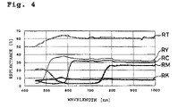
- FIG. 4 is a graph showing reflection characteristics of each toner as compared to wavelength of light.
- FIGS. 5( a ) and 5 ( b ) are graphs showing the interference state of a toner carrier and toner when reflecting light is irradiated from a front area and a rear area, respectively.
- FIG. 6 is a graph showing the occurrence state of reflected light for positional detection generated by a multi color image forming apparatus made in accordance with principles of the disclosed subject matter.
- FIG. 7( a ) is an explanatory view showing another embodiment of an optical sensor made in accordance with principles of the disclosed subject matter.
- FIG. 7( b ) is an explanatory view showing yet another embodiment of an optical sensor made in accordance with principles of the disclosed subject matter.
- FIG. 8 is an explanatory view showing another embodiment of an optical sensor made in accordance with principles of the disclosed subject matter.
- FIG. 9 is an explanatory view showing a conventional example of a multi-color image-forming apparatus.
- FIG. 1 is a multi-color image-forming apparatus 20 made in accordance with principles of the disclosed subject matter, and includes a toner carrier 10 .
- Patterns 1 C, 1 m, 1 Y, and 1 K for detecting toner position for each color (C, M, Y and K) are provided on the toner carrier 10 , and an image is formed by using the patterns for detecting toner position 1 (C, M, Y, K) as a reference.
- the description of components widely known for image forming such as a drum and exposure means is omitted in FIG. 1 .
- the image forming apparatus can also include a control unit 31 that is configured to control operation of the multi-color image-forming apparatus.
- the control unit can be programmed such that it controls the apparatus to produce at least one high reflectance pattern and at least one low reflectance pattern on the toner carrier in accordance with principles of the disclosed subject matter.
- toner having high reflectance to the emission wavelength of the light-emitting element can be used to form the patterns for detecting toner position 1 , independently, as shown with the magenta toner pattern 1 M and yellow toner pattern 1 Y of FIG. 2 .
- a foundation 2 can be formed by toner having high reflectance.
- the foundation can be located adjacent toner having low reflectance to the light emission wavelength (cyan toner and black toner in the case of the red LED, for example).
- a cyan toner pattern 1 C can be formed on the central portion of the upper surface of a magenta foundation 2 M and a black toner pattern 1 K can be formed on the central portion of the upper surface of a yellow foundation 2 Y, as shown in FIG. 2 .
- Simple line shapes used for the pattern(s) are shown in FIG. 2 .
- various other shapes such as wedge shape(s), a cross shape(s), etc., are considered for use as the pattern(s) for detecting toner position (C, M, Y, K) for each color.
- the disclosed subject matter can be characterized in that the pattern(s) for detecting toner position which exhibit low reflectance to the light from the light source, can be formed on the foundation 2 which has high reflectance, in substantially any shape.
- the toner (C, M, Y, K) can be used for both the patterns for detecting toner position 1 and the foundation 2 .
- FIG. 3( a ) shows the constitution of an optical sensor 3 that is configured to detect the patterns for detecting toner position, and can include: a light-emitting element 3 a such as an LED or a laser diode; a polarizing optical element 3 b that is configured to cast only light whose polarized direction is uniform from the light that is irradiated from the light-emitting element 3 a ; a light-receiving element 3 c arranged so as to take in only a normal reflection component from the light reflected from the detection target; and a polarizing optical element 3 d configured to permit substantially only a polarized component that is different from the light cast onto the detection target to be incident on the light-receiving element 3 c .
- the polarizing optical element 3 b can be omitted when the light-emitting element 3 a is a laser diode, as shown in FIG. 3( b ).
- FIG. 4 is a graph showing the spectral reflectance of toner of each color, in which a curve RM, a curve RC, a curve RY, a curve RK and a curve RT respectively show the spectral reflectance for the magenta toner, the cyan toner, the yellow toner, the black toner, and the toner carrier. Therefore, detected sensitivity in each wavelength is a value obtained by subtracting the reflectance of the toner from the reflectance of the curve RT of the same wavelength. As can be seen, a considerable difference exists between numerical values obtained at different wavelengths.
- the emission wavelength of the light-emitting element 3 a should be about 620 to 720 nm of red color considering the spectral reflectance of toner of each color shown in FIG. 4 , the reflectance of the toner carrier 10 , and the cost of the polarizing optical elements 3 b , 3 d .
- it may be about 800 to 1000 nm of infrared light, and in this case, the foundation 2 is not necessary for the cyan toner pattern C and the foundation can be provided only for the black toner pattern 1 K.
- a PD (photodiode) and a phototransistor can be used as the light-receiving element 3 c.
- the reflected light from the toner carrier 10 was made incident to the light-receiving element 3 c .
- An output difference (dynamic range) of the light-receiving element 3 c for cases with and without the patterns for detecting toner position (C, M, Y, K) was limited in a narrow range.
- the output from the light-receiving element 3 c when the patterns for detecting toner position do not exist becomes substantially zero.
- the output from the light-receiving element 3 c that measures the reflected light quantity from the patterns for detecting toner position also increases substantially in proportion to the increase of the light quantity, so that the dynamic range of a light-receiving output can be easily widened, S/N ratio increases, and thus pattern detection accuracy can be improved.
- the compound effect of the reflected light from the toner carrier 10 and the reflected light from the edge of the patterns for detecting toner position (C, M, Y, K) causes ripple(s) in output wavelength when detecting the vicinity of the patterns for detecting toner position (C, M, Y, K).
- the ripple may be strongly affected by a positional relationship between the detection target and the sensor, particularly from an irradiating direction, where the ripple is caused in the front area of detected wavelength output as shown by a curve C (+5) in FIG. 5(A) when light is irradiated from an area closer to the front.
- the ripple can be caused in the rear area of the detected wavelength output as shown by a curve C ( ⁇ 5) in FIG. 5(B) when light is irradiated from an area closer to the rear.
- toner having high reflectance when toner having high reflectance is used as a foundation for toner having low reflectance, positional detection to the toner having high reflectance is performed by convex portions of output, and positional detection to the toner having low reflectance is performed by concave portions in the reflected light from the foundation 2 .
- FIG. 7( a ) shows another embodiment of an optical sensor 3 made in accordance with principles of the disclosed subject matter.
- the polarizing optical element 3 b for casting light was installed so as to be orthogonal to axis X of the light-emitting element 3 a
- the polarizing optical element 3 d for receiving light was installed to be orthogonal to axis Y of the light-receiving element 3 c .
- the polarizing optical element 3 b for casting light and the polarizing optical element 3 d for receiving light are installed substantially parallel to the toner carrier 10 in the embodiment of FIGS. 7( a )-( b ). Note that the polarizing optical element 3 b for casting light can be omitted when the light-emitting element 3 a is a laser diode, as shown in FIG. 7( b ).
- the polarizing optical elements for casting light and receiving light 3 b , 3 d may be arranged in parallel or, alternatively, a polarizing beam splitter 3 e may also be used as shown in the embodiment of FIG. 8 .
- a polarizing beam splitter 3 e When the polarizing beam splitter 3 e is used, light (from an area other than light to be cast onto the detection target from the light emitted from the light-emitting element 3 a ) can be made incident to a light-receiving element 3 f for monitoring, as shown by a broken line in FIG. 8 .
- feedback control may be provided to the light-emitting element 3 a so as to fix output, for example.
- the disclosed subject matter is applicable for a color image forming apparatus such as a copying machine and a printer, which utilizes an electrophotograph system and also for a use where a color image is formed by accurately superposing dots or the like of cyan (C), magenta (M), yellow (Y) and black (K).
Landscapes
- Engineering & Computer Science (AREA)
- Microelectronics & Electronic Packaging (AREA)
- Physics & Mathematics (AREA)
- General Physics & Mathematics (AREA)
- Color Electrophotography (AREA)
- Control Or Security For Electrophotography (AREA)
- Length Measuring Devices By Optical Means (AREA)
Applications Claiming Priority (2)
| Application Number | Priority Date | Filing Date | Title |
|---|---|---|---|
| JP2005-306870 | 2005-10-21 | ||
| JP2005306870A JP4945111B2 (ja) | 2005-10-21 | 2005-10-21 | 多色画像形成装置及び同装置用光センサ |
Publications (2)
| Publication Number | Publication Date |
|---|---|
| US20070110485A1 US20070110485A1 (en) | 2007-05-17 |
| US7689151B2 true US7689151B2 (en) | 2010-03-30 |
Family
ID=38040956
Family Applications (1)
| Application Number | Title | Priority Date | Filing Date |
|---|---|---|---|
| US11/550,905 Expired - Fee Related US7689151B2 (en) | 2005-10-21 | 2006-10-19 | Multi-color image-forming apparatus, optical sensor, and method for the same |
Country Status (2)
| Country | Link |
|---|---|
| US (1) | US7689151B2 (ja) |
| JP (1) | JP4945111B2 (ja) |
Cited By (5)
| Publication number | Priority date | Publication date | Assignee | Title |
|---|---|---|---|---|
| US20080089706A1 (en) * | 2006-10-12 | 2008-04-17 | Canon Kabushiki Kaisha | Image forming apparatus |
| US20110280633A1 (en) * | 2010-05-17 | 2011-11-17 | Canon Kabushiki Kaisha | Image forming apparatus |
| US20130064564A1 (en) * | 2011-09-09 | 2013-03-14 | Fuji Xerox Co., Ltd. | Registration mark and image forming apparatus |
| US20130287457A1 (en) * | 2012-04-27 | 2013-10-31 | Canon Kabushiki Kaisha | Image forming apparatus |
| US20170235266A1 (en) * | 2016-02-16 | 2017-08-17 | Canon Kabushiki Kaisha | Image forming apparatus for correcting color misregistration |
Families Citing this family (6)
| Publication number | Priority date | Publication date | Assignee | Title |
|---|---|---|---|---|
| US7848690B2 (en) * | 2007-07-31 | 2010-12-07 | Samsung Electronics Co., Ltd. | Image forming apparatus and auto color registration method thereof |
| US8036552B2 (en) * | 2007-09-21 | 2011-10-11 | Canon Kabushiki Kaisha | Method for correcting registration errors by superimposing a black developer on a background of a color |
| JP5254815B2 (ja) | 2009-01-08 | 2013-08-07 | スタンレー電気株式会社 | 多色画像形成装置及び位置検出用色画像パターン検出プログラム |
| JP5747436B2 (ja) * | 2009-09-10 | 2015-07-15 | 株式会社リコー | 位置ずれ補正装置及び画像形成装置 |
| JP5893377B2 (ja) * | 2011-12-09 | 2016-03-23 | キヤノン株式会社 | 画像形成装置 |
| JP2015075619A (ja) * | 2013-10-09 | 2015-04-20 | 京セラドキュメントソリューションズ株式会社 | トナー濃度センサー及び画像形成装置 |
Citations (4)
| Publication number | Priority date | Publication date | Assignee | Title |
|---|---|---|---|---|
| JPH01167769A (ja) | 1987-12-23 | 1989-07-03 | Canon Inc | 多重画像形成装置 |
| US6658221B2 (en) * | 2001-01-19 | 2003-12-02 | Seiko Epson Corporation | Method of and apparatus for measuring quantity of toner on belt-shaped image carrier |
| US6687472B2 (en) * | 2002-04-30 | 2004-02-03 | Fuji Xerox Co., Ltd. | Image forming apparatus and color-shift control method |
| US6853817B2 (en) * | 2001-08-31 | 2005-02-08 | Canon Kabushiki Kaisha | Method for correcting and controlling image forming conditions |
Family Cites Families (3)
| Publication number | Priority date | Publication date | Assignee | Title |
|---|---|---|---|---|
| JP2993556B2 (ja) * | 1995-12-20 | 1999-12-20 | 富士ゼロックス株式会社 | カラー画像出力装置 |
| JP2002156463A (ja) * | 2000-11-17 | 2002-05-31 | Konica Corp | 物体識別方法、物体識別センサおよび画像形成装置 |
| JP2004302167A (ja) * | 2003-03-31 | 2004-10-28 | Ricoh Co Ltd | 画質検出装置、画像形成装置、画質検出方法、コンピュータプログラム及び記録媒体 |
-
2005
- 2005-10-21 JP JP2005306870A patent/JP4945111B2/ja not_active Expired - Fee Related
-
2006
- 2006-10-19 US US11/550,905 patent/US7689151B2/en not_active Expired - Fee Related
Patent Citations (4)
| Publication number | Priority date | Publication date | Assignee | Title |
|---|---|---|---|---|
| JPH01167769A (ja) | 1987-12-23 | 1989-07-03 | Canon Inc | 多重画像形成装置 |
| US6658221B2 (en) * | 2001-01-19 | 2003-12-02 | Seiko Epson Corporation | Method of and apparatus for measuring quantity of toner on belt-shaped image carrier |
| US6853817B2 (en) * | 2001-08-31 | 2005-02-08 | Canon Kabushiki Kaisha | Method for correcting and controlling image forming conditions |
| US6687472B2 (en) * | 2002-04-30 | 2004-02-03 | Fuji Xerox Co., Ltd. | Image forming apparatus and color-shift control method |
Cited By (12)
| Publication number | Priority date | Publication date | Assignee | Title |
|---|---|---|---|---|
| US20080089706A1 (en) * | 2006-10-12 | 2008-04-17 | Canon Kabushiki Kaisha | Image forming apparatus |
| US8565634B2 (en) * | 2006-10-12 | 2013-10-22 | Canon Kabushiki Kaisha | Image forming apparatus |
| US20110280633A1 (en) * | 2010-05-17 | 2011-11-17 | Canon Kabushiki Kaisha | Image forming apparatus |
| US8744325B2 (en) * | 2010-05-17 | 2014-06-03 | Canon Kabushiki Kaisha | Image forming apparatus for forming a detection toner pattern |
| US20130064564A1 (en) * | 2011-09-09 | 2013-03-14 | Fuji Xerox Co., Ltd. | Registration mark and image forming apparatus |
| US8811845B2 (en) * | 2011-09-09 | 2014-08-19 | Fuji Xerox Co., Ltd. | Registration mark and image forming apparatus |
| US20130287457A1 (en) * | 2012-04-27 | 2013-10-31 | Canon Kabushiki Kaisha | Image forming apparatus |
| US8995892B2 (en) * | 2012-04-27 | 2015-03-31 | Canon Kabushiki Kaisha | Image forming apparatus with threshold adjustment for superposed measurement images |
| US20150147078A1 (en) * | 2012-04-27 | 2015-05-28 | Canon Kabushiki Kaisha | Image forming apparatus |
| US9229404B2 (en) * | 2012-04-27 | 2016-01-05 | Canon Kabushiki Kaisha | Image forming apparatus |
| US20170235266A1 (en) * | 2016-02-16 | 2017-08-17 | Canon Kabushiki Kaisha | Image forming apparatus for correcting color misregistration |
| US10031459B2 (en) * | 2016-02-16 | 2018-07-24 | Canon Kabushiki Kaisha | Image forming apparatus for correcting color misregistration |
Also Published As
| Publication number | Publication date |
|---|---|
| US20070110485A1 (en) | 2007-05-17 |
| JP2007114555A (ja) | 2007-05-10 |
| JP4945111B2 (ja) | 2012-06-06 |
Similar Documents
| Publication | Publication Date | Title |
|---|---|---|
| US7689151B2 (en) | Multi-color image-forming apparatus, optical sensor, and method for the same | |
| US8136904B2 (en) | Apparatus to control color registration and image density | |
| US9927752B2 (en) | Optical sensor and image forming apparatus | |
| JP6061703B2 (ja) | 光学センサ及び画像形成装置 | |
| US8971749B2 (en) | Optical sensor and image forming apparatus | |
| US8472019B2 (en) | Spectroscopic characteristics acquisition unit, image evaluation unit, and image forming apparatus | |
| US20070003302A1 (en) | Image quality measurements using linear array in specular mode | |
| US7027139B2 (en) | Photosensor apparatus and image forming apparatus | |
| US20130216245A1 (en) | Optical sensor and image forming apparatus | |
| US20180292776A1 (en) | Optical sensor and image forming apparatus | |
| US5896472A (en) | Image forming apparatus | |
| US6674988B2 (en) | Toner misregistration detection sensor, color image-forming apparatus using the same, and method for toner misregistration detection | |
| JP2007156159A (ja) | 色ずれ検出センサ及び色ずれ検出装置 | |
| JP6471437B2 (ja) | 撮像装置、測色装置および画像形成装置 | |
| JP3843636B2 (ja) | 光量測定装置及びカラー画像形成装置 | |
| US20210278792A1 (en) | Image forming apparatus that obtains color misregistration amount using detection result of test image | |
| JP2006025359A (ja) | 画像形成装置および画像形成方法 | |
| US6101359A (en) | Image forming apparatus | |
| JP2001343287A (ja) | 光学測定装置及びカラー画像形成装置 | |
| JP2017103497A (ja) | 光学センサ及び画像形成装置 | |
| US20050104950A1 (en) | Apparatus to control color registration and image density using a single mark and method using the same | |
| JPH10142863A (ja) | 画像形成装置 | |
| JP2019144020A (ja) | 検知装置、及び画像形成装置 | |
| JP7449158B2 (ja) | 画像形成装置 | |
| US20230291842A1 (en) | Information processing apparatus, abnormality detection method, storage medium, and information processing system |
Legal Events
| Date | Code | Title | Description |
|---|---|---|---|
| AS | Assignment |
Owner name: STANLEY ELECTRIC CO., LTD.,JAPAN Free format text: ASSIGNMENT OF ASSIGNORS INTEREST;ASSIGNORS:KATSUHARA, KENJI;MOTOHIRA, KATSUYA;OGAWA, FUMIO;SIGNING DATES FROM 20061030 TO 20061115;REEL/FRAME:018544/0783 Owner name: KYOCERA MITA CORPORATION,JAPAN Free format text: ASSIGNMENT OF ASSIGNORS INTEREST;ASSIGNORS:KATSUHARA, KENJI;MOTOHIRA, KATSUYA;OGAWA, FUMIO;SIGNING DATES FROM 20061030 TO 20061115;REEL/FRAME:018544/0783 |
|
| FEPP | Fee payment procedure |
Free format text: PAYOR NUMBER ASSIGNED (ORIGINAL EVENT CODE: ASPN); ENTITY STATUS OF PATENT OWNER: LARGE ENTITY |
|
| FPAY | Fee payment |
Year of fee payment: 4 |
|
| FEPP | Fee payment procedure |
Free format text: MAINTENANCE FEE REMINDER MAILED (ORIGINAL EVENT CODE: REM.) |
|
| LAPS | Lapse for failure to pay maintenance fees |
Free format text: PATENT EXPIRED FOR FAILURE TO PAY MAINTENANCE FEES (ORIGINAL EVENT CODE: EXP.) |
|
| STCH | Information on status: patent discontinuation |
Free format text: PATENT EXPIRED DUE TO NONPAYMENT OF MAINTENANCE FEES UNDER 37 CFR 1.362 |
|
| FP | Lapsed due to failure to pay maintenance fee |
Effective date: 20180330 |