US7687793B2 - Resistance variable memory cells - Google Patents
Resistance variable memory cells Download PDFInfo
- Publication number
- US7687793B2 US7687793B2 US11/751,896 US75189607A US7687793B2 US 7687793 B2 US7687793 B2 US 7687793B2 US 75189607 A US75189607 A US 75189607A US 7687793 B2 US7687793 B2 US 7687793B2
- Authority
- US
- United States
- Prior art keywords
- conductive material
- layer
- chalcogenide
- memory
- memory cell
- Prior art date
- Legal status (The legal status is an assumption and is not a legal conclusion. Google has not performed a legal analysis and makes no representation as to the accuracy of the status listed.)
- Expired - Fee Related, expires
Links
- 230000015654 memory Effects 0.000 title claims description 124
- 239000000463 material Substances 0.000 claims abstract description 97
- 150000004770 chalcogenides Chemical class 0.000 claims abstract description 85
- 239000004020 conductor Substances 0.000 claims abstract description 64
- 229910052709 silver Inorganic materials 0.000 claims abstract description 35
- 239000004332 silver Substances 0.000 claims abstract description 35
- RYGMFSIKBFXOCR-UHFFFAOYSA-N Copper Chemical compound [Cu] RYGMFSIKBFXOCR-UHFFFAOYSA-N 0.000 claims abstract description 9
- 229910052802 copper Inorganic materials 0.000 claims abstract description 9
- 239000010949 copper Substances 0.000 claims abstract description 9
- 150000002500 ions Chemical class 0.000 claims abstract description 9
- 239000003989 dielectric material Substances 0.000 claims description 22
- 239000000758 substrate Substances 0.000 claims description 16
- 238000007654 immersion Methods 0.000 claims description 15
- QIHHYQWNYKOHEV-UHFFFAOYSA-N 4-tert-butyl-3-nitrobenzoic acid Chemical compound CC(C)(C)C1=CC=C(C(O)=O)C=C1[N+]([O-])=O QIHHYQWNYKOHEV-UHFFFAOYSA-N 0.000 claims description 14
- PXHVJJICTQNCMI-UHFFFAOYSA-N Nickel Chemical compound [Ni] PXHVJJICTQNCMI-UHFFFAOYSA-N 0.000 claims description 9
- 229910052759 nickel Inorganic materials 0.000 claims description 5
- WFKWXMTUELFFGS-UHFFFAOYSA-N tungsten Chemical compound [W] WFKWXMTUELFFGS-UHFFFAOYSA-N 0.000 claims description 5
- 229910052721 tungsten Inorganic materials 0.000 claims description 5
- 239000010937 tungsten Substances 0.000 claims description 5
- 229910052782 aluminium Inorganic materials 0.000 claims description 4
- XAGFODPZIPBFFR-UHFFFAOYSA-N aluminium Chemical compound [Al] XAGFODPZIPBFFR-UHFFFAOYSA-N 0.000 claims description 4
- 230000037361 pathway Effects 0.000 claims 2
- 230000004044 response Effects 0.000 claims 1
- 238000000034 method Methods 0.000 abstract description 22
- 230000008569 process Effects 0.000 abstract description 12
- 238000007747 plating Methods 0.000 abstract description 10
- 238000006243 chemical reaction Methods 0.000 abstract description 4
- 210000004027 cell Anatomy 0.000 description 68
- BQCADISMDOOEFD-UHFFFAOYSA-N Silver Chemical compound [Ag] BQCADISMDOOEFD-UHFFFAOYSA-N 0.000 description 32
- 238000004519 manufacturing process Methods 0.000 description 17
- 229910052751 metal Inorganic materials 0.000 description 17
- 239000002184 metal Substances 0.000 description 17
- 229910021645 metal ion Inorganic materials 0.000 description 9
- 239000010953 base metal Substances 0.000 description 8
- 230000006870 function Effects 0.000 description 8
- 238000005229 chemical vapour deposition Methods 0.000 description 7
- 229910000510 noble metal Inorganic materials 0.000 description 6
- 239000011159 matrix material Substances 0.000 description 5
- 230000005855 radiation Effects 0.000 description 5
- 239000000126 substance Substances 0.000 description 5
- VYPSYNLAJGMNEJ-UHFFFAOYSA-N Silicium dioxide Chemical compound O=[Si]=O VYPSYNLAJGMNEJ-UHFFFAOYSA-N 0.000 description 4
- 210000001787 dendrite Anatomy 0.000 description 4
- -1 i.e. Substances 0.000 description 4
- 239000004065 semiconductor Substances 0.000 description 4
- 238000003860 storage Methods 0.000 description 4
- 230000008859 change Effects 0.000 description 3
- 238000000151 deposition Methods 0.000 description 3
- 239000011521 glass Substances 0.000 description 3
- 229910052581 Si3N4 Inorganic materials 0.000 description 2
- 230000002411 adverse Effects 0.000 description 2
- 230000008901 benefit Effects 0.000 description 2
- 238000004891 communication Methods 0.000 description 2
- 238000011161 development Methods 0.000 description 2
- 230000018109 developmental process Effects 0.000 description 2
- 238000010586 diagram Methods 0.000 description 2
- 239000010416 ion conductor Substances 0.000 description 2
- 150000002739 metals Chemical class 0.000 description 2
- 238000012986 modification Methods 0.000 description 2
- 230000004048 modification Effects 0.000 description 2
- 239000012782 phase change material Substances 0.000 description 2
- BASFCYQUMIYNBI-UHFFFAOYSA-N platinum Chemical compound [Pt] BASFCYQUMIYNBI-UHFFFAOYSA-N 0.000 description 2
- 235000012239 silicon dioxide Nutrition 0.000 description 2
- 239000000377 silicon dioxide Substances 0.000 description 2
- HQVNEWCFYHHQES-UHFFFAOYSA-N silicon nitride Chemical compound N12[Si]34N5[Si]62N3[Si]51N64 HQVNEWCFYHHQES-UHFFFAOYSA-N 0.000 description 2
- 238000001228 spectrum Methods 0.000 description 2
- 238000004544 sputter deposition Methods 0.000 description 2
- 241001101998 Galium Species 0.000 description 1
- 229910045601 alloy Inorganic materials 0.000 description 1
- 239000000956 alloy Substances 0.000 description 1
- 229910052787 antimony Inorganic materials 0.000 description 1
- 239000003054 catalyst Substances 0.000 description 1
- 230000001413 cellular effect Effects 0.000 description 1
- 235000019504 cigarettes Nutrition 0.000 description 1
- 238000013461 design Methods 0.000 description 1
- 238000009826 distribution Methods 0.000 description 1
- 230000005611 electricity Effects 0.000 description 1
- 229910052732 germanium Inorganic materials 0.000 description 1
- PCHJSUWPFVWCPO-UHFFFAOYSA-N gold Chemical compound [Au] PCHJSUWPFVWCPO-UHFFFAOYSA-N 0.000 description 1
- 229910052737 gold Inorganic materials 0.000 description 1
- 239000010931 gold Substances 0.000 description 1
- 238000005342 ion exchange Methods 0.000 description 1
- 239000003446 ligand Substances 0.000 description 1
- 238000001465 metallisation Methods 0.000 description 1
- 150000002825 nitriles Chemical class 0.000 description 1
- 230000000737 periodic effect Effects 0.000 description 1
- 230000002093 peripheral effect Effects 0.000 description 1
- 238000005240 physical vapour deposition Methods 0.000 description 1
- 238000000623 plasma-assisted chemical vapour deposition Methods 0.000 description 1
- 229910052697 platinum Inorganic materials 0.000 description 1
- 230000008672 reprogramming Effects 0.000 description 1
- 230000000717 retained effect Effects 0.000 description 1
- 230000002441 reversible effect Effects 0.000 description 1
- 229910052711 selenium Inorganic materials 0.000 description 1
- 229910052710 silicon Inorganic materials 0.000 description 1
- 239000010703 silicon Substances 0.000 description 1
- 150000003378 silver Chemical class 0.000 description 1
- 230000003068 static effect Effects 0.000 description 1
- 229910052714 tellurium Inorganic materials 0.000 description 1
Images


Classifications
-
- H—ELECTRICITY
- H01—ELECTRIC ELEMENTS
- H01L—SEMICONDUCTOR DEVICES NOT COVERED BY CLASS H10
- H01L21/00—Processes or apparatus adapted for the manufacture or treatment of semiconductor or solid state devices or of parts thereof
- H01L21/02—Manufacture or treatment of semiconductor devices or of parts thereof
- H01L21/04—Manufacture or treatment of semiconductor devices or of parts thereof the devices having potential barriers, e.g. a PN junction, depletion layer or carrier concentration layer
- H01L21/18—Manufacture or treatment of semiconductor devices or of parts thereof the devices having potential barriers, e.g. a PN junction, depletion layer or carrier concentration layer the devices having semiconductor bodies comprising elements of Group IV of the Periodic Table or AIIIBV compounds with or without impurities, e.g. doping materials
- H01L21/28—Manufacture of electrodes on semiconductor bodies using processes or apparatus not provided for in groups H01L21/20 - H01L21/268
- H01L21/283—Deposition of conductive or insulating materials for electrodes conducting electric current
- H01L21/288—Deposition of conductive or insulating materials for electrodes conducting electric current from a liquid, e.g. electrolytic deposition
-
- H—ELECTRICITY
- H10—SEMICONDUCTOR DEVICES; ELECTRIC SOLID-STATE DEVICES NOT OTHERWISE PROVIDED FOR
- H10N—ELECTRIC SOLID-STATE DEVICES NOT OTHERWISE PROVIDED FOR
- H10N70/00—Solid-state devices having no potential barriers, and specially adapted for rectifying, amplifying, oscillating or switching
- H10N70/011—Manufacture or treatment of multistable switching devices
- H10N70/021—Formation of switching materials, e.g. deposition of layers
- H10N70/023—Formation of switching materials, e.g. deposition of layers by chemical vapor deposition, e.g. MOCVD, ALD
-
- H—ELECTRICITY
- H10—SEMICONDUCTOR DEVICES; ELECTRIC SOLID-STATE DEVICES NOT OTHERWISE PROVIDED FOR
- H10N—ELECTRIC SOLID-STATE DEVICES NOT OTHERWISE PROVIDED FOR
- H10N70/00—Solid-state devices having no potential barriers, and specially adapted for rectifying, amplifying, oscillating or switching
- H10N70/011—Manufacture or treatment of multistable switching devices
- H10N70/041—Modification of switching materials after formation, e.g. doping
- H10N70/043—Modification of switching materials after formation, e.g. doping by implantation
-
- H—ELECTRICITY
- H10—SEMICONDUCTOR DEVICES; ELECTRIC SOLID-STATE DEVICES NOT OTHERWISE PROVIDED FOR
- H10N—ELECTRIC SOLID-STATE DEVICES NOT OTHERWISE PROVIDED FOR
- H10N70/00—Solid-state devices having no potential barriers, and specially adapted for rectifying, amplifying, oscillating or switching
- H10N70/20—Multistable switching devices, e.g. memristors
- H10N70/24—Multistable switching devices, e.g. memristors based on migration or redistribution of ionic species, e.g. anions, vacancies
- H10N70/245—Multistable switching devices, e.g. memristors based on migration or redistribution of ionic species, e.g. anions, vacancies the species being metal cations, e.g. programmable metallization cells
-
- H—ELECTRICITY
- H10—SEMICONDUCTOR DEVICES; ELECTRIC SOLID-STATE DEVICES NOT OTHERWISE PROVIDED FOR
- H10N—ELECTRIC SOLID-STATE DEVICES NOT OTHERWISE PROVIDED FOR
- H10N70/00—Solid-state devices having no potential barriers, and specially adapted for rectifying, amplifying, oscillating or switching
- H10N70/801—Constructional details of multistable switching devices
- H10N70/821—Device geometry
- H10N70/826—Device geometry adapted for essentially vertical current flow, e.g. sandwich or pillar type devices
-
- H—ELECTRICITY
- H10—SEMICONDUCTOR DEVICES; ELECTRIC SOLID-STATE DEVICES NOT OTHERWISE PROVIDED FOR
- H10N—ELECTRIC SOLID-STATE DEVICES NOT OTHERWISE PROVIDED FOR
- H10N70/00—Solid-state devices having no potential barriers, and specially adapted for rectifying, amplifying, oscillating or switching
- H10N70/801—Constructional details of multistable switching devices
- H10N70/881—Switching materials
- H10N70/882—Compounds of sulfur, selenium or tellurium, e.g. chalcogenides
- H10N70/8825—Selenides, e.g. GeSe
Definitions
- the invention relates generally to the field of semiconductor devices and fabrication and, more particularly, to memory elements and methods for making memory elements.
- Microprocessor-controlled integrated circuits are used in a wide variety of applications. Such applications include personal computers, vehicle control systems, telephone networks, and a host of consumer products. As is well known, microprocessors are essentially generic devices that perform specific functions under the control of a software program. This program is stored in one or more memory devices that are coupled to the microprocessor. Not only does the microprocessor access memory devices to retrieve the program instructions, but it also stores and retrieves data created during execution of the program in one or more memory devices.
- NVRAM nonvolatile random access memory
- phase change materials can be electrically switched between a first structural state, in which the material is generally amorphous, and a second structural state, in which the material has a generally crystalline local order.
- the material may also be electrically switched between different detectable states of local order across the entire spectrum between the completely amorphous and the completely crystalline states.
- the switching of such materials is not required to take place in a binary fashion between completely amorphous and completely crystalline states.
- the material may be switched in incremental steps reflecting changes of local order to provide a “gray scale” represented by a multiplicity of conditions of local order spanning the spectrum from the completely amorphous state to the completely crystalline state.
- These memory elements are monolithic, homogeneous, and formed of chalcogenide material typically selected from the group of Te, Se, Sb, Ni, and Ge.
- This chalcogenide material exhibits different electrical characteristics depending upon its state. For instance, in its amorphous state the material exhibits a higher resistivity than it does in its crystalline state.
- Such chalcogenide materials may be switched between numerous electrically detectable conditions of varying resistivity in nanosecond time periods with the input of picojoules of energy.
- the resulting memory element is truly non-volatile. It will maintain the integrity of the information stored by the memory cell without the need for periodic refresh signals, and the data integrity of the information stored by these memory cells is not lost when power is removed from the device.
- the memory material is also directly overwritable so that the memory cells need not be erased, i.e., set to a specified starting point, in order to change information stored within the memory cells.
- the large dynamic range offered by the memory material theoretically provides for the gray scale storage of multiple bits of binary information in a single cell by mimicking the binary encoded information in analog form and, thereby, storing multiple bits of binary encoded information as a single resistance value in a single cell.
- chalcogenide memory cells require that a region of the chalcogenide memory material, called the “active region,” be subjected to a current pulse to change the crystalline state of the chalcogenide material within the active region.
- a current density typically of between about 10 5 and 10 7 amperes/cm 2 is needed.
- the active region of each memory cell should be made as small as possible to minimize the total current drawn by the memory device.
- Such traditional chalcogenide memory cells have evolved into what is referred to as a programmable metallization cell or a plated chalcogenide memory cell for use in a plated chalcogenide random access memory (PCRAM) device.
- a cell includes a chalcogenide material between opposing electrodes.
- a fast ion conductor material is incorporated into the chalcogenide material. The resistance of such material can be changed between highly resistive and highly conductive states.
- a voltage potential is applied to a certain one of the electrodes, with the other of the electrode being held at zero voltage or ground.
- the electrode having the voltage applied to it functions as an anode, while the electrode held at zero or ground functions as a cathode.
- the nature of the fast ion conductor material is such that it undergoes a chemical and structural change at a certain applied voltage level. Specifically, at some suitable threshold voltage, the metal ions within the chalcogenide material begin to plate on the cathode and progress through the chalcogenide material toward the anode. The process continues until a conductive dendrite or filament extends between the electrodes, effectively interconnecting the top and bottom electrodes to create an electrical short circuit.
- such a device can, for example, function as a reprogrammable memory cell of non-volatile random access memory circuit.
- the variable resistance material disposed between the electrodes typically is a chalcogenide material having metal ions diffused therein.
- a specific example is germanium selenide with silver ions.
- germanium selenide is deposited onto the first electrode using chemical vapor deposition.
- a thin layer of silver is then deposited on the glass, for example by physical vapor deposition or another technique.
- the layer of silver is then irradiated with ultraviolet radiation.
- the thin nature of the deposited silver allows the energy to pass through the silver to the silver/glass interface to cause the silver to diffuse into the chalcogenide material.
- the applied energy and overlying silver result in the silver migrating into the glass layer such that a homegenous distribution of silver throughout the layer is ultimately achieved.
- chalcogenide materials are relatively delicate. The nature of the deposition technique used to deposit the silver can damage the chalcogenide material and, thus, adversely affect the resulting memory cell. Furthermore, it can be challenging to etch and polish chalcogenide materials. Accordingly, it would be desirable to develop memory cell fabrication methods that avoid steps that can damage such materials.
- FIG. 1 illustrates a block diagram of an exemplary processor-based device
- FIG. 2 illustrates an exemplary memory device
- FIG. 3 illustrates a more detailed view of the memory array of the memory device illustrated in FIG. 2 ;
- FIGS. 4-10 illustrate cross-sectional views of a memory cell during different stages of fabrication
- FIGS. 11-15 illustrate cross-sectional views of an alternate embodiment of a memory cell during different stages of fabrication.
- FIGS. 16-19 illustrate cross-sectional views of another alternate embodiment of a memory cell during different stages of fabrication.
- FIG. 1 a block diagram depicting an exemplary processor-based device, generally designated by the reference numeral 10 , is illustrated.
- the device 10 may be any of a variety of different types, such as a computer, pager, cellular telephone, personal organizer, control circuit, etc.
- processors 12 such as a microprocessor(s), control many of the functions of the device 10 .
- the device 10 typically includes a power supply 14 .
- the power supply 14 would advantageously include permanent batteries, replaceable batteries, and/or rechargeable batteries.
- the power supply 14 may also include an A/C adapter, so that the device may be plugged into a wall outlet, for instance.
- the power supply 14 may also include a D/C adapter, so that the device 10 may be plugged into a vehicle's cigarette lighter, for instance.
- a user interface 16 may be coupled to the processor(s) 12 .
- the user interface 16 may include an input device, such as buttons, switches, a keyboard, a light pin, a mouse, and/or a voice recognition system, for instance.
- a display 18 may also be coupled to the processor(s) 12 .
- the display 18 may include an LCD display, a CRT, LEDs, and/or an audio display.
- an RF subsystem/baseband processor 20 may also be coupled to the processor(s) 12 .
- the RF subsystem/baseband processor 20 may include an antenna that is coupled to an RF receiver and to an RF transmitter (not shown).
- a communication port 22 may also be coupled to the processor(s) 12 .
- the communication port 22 may be adapted to be coupled to a peripheral device 24 , such as a modem, a printer, or a computer, for instance, or to a network, such as a local area network or the Internet.
- memory is coupled to the processor(s) 12 to store and facilitate execution of the software program.
- the processor(s) 12 may be coupled to volatile memory 26 , which may include dynamic random access memory (DRAM), static random access memory (SRAM), Double Data Rate (DDR) memory, etc.
- volatile memory 26 may include dynamic random access memory (DRAM), static random access memory (SRAM), Double Data Rate (DDR) memory, etc.
- the processor(s) 12 may also be coupled to non-volatile memory 28 .
- the non-volatile memory 28 may include a read only memory (ROM), such as an EPROM or Flash Memory, to be used in conjunction with the volatile memory.
- ROM read only memory
- the size of the ROM is typically selected to be just large enough to store any necessary operating system, application programs, and fixed data.
- the volatile memory is typically quite large so that it can store dynamically loaded applications.
- the non-volatile memory 28 may include a high capacity memory such as a disk drive, tape drive memory, CD ROM drive, DVD, read/write CD ROM drive, and/or a floppy disk drive.
- the memory device 30 is an integrated circuit memory that is advantageously formed on a semiconductor substrate 32 .
- the memory device 30 includes a memory matrix or array 34 that includes a plurality of memory cells for storing data, as described below.
- the memory matrix 34 is coupled to periphery circuitry 36 by the plurality of control lines 38 .
- the periphery circuitry 36 may include circuitry for addressing the memory cells contained within the memory matrix 34 , along with circuitry for storing data in and retrieving data from the memory cells.
- the periphery circuitry 36 may also include other circuitry used for controlling or otherwise insuring the proper functioning of the memory device 30 .
- the memory matrix 34 includes a plurality of memory cells 40 that are arranged in generally perpendicular rows and columns.
- the memory cells 40 in each row are coupled together by a respective word line 42
- the memory cells 40 in each column are coupled together by a respective digit line 44 .
- each memory cell 40 includes a word line node 46 that is coupled to a respective word line 42
- each memory cell 40 includes a digit line node 48 that is coupled to a respective digit line 44 .
- the conductive word lines 42 and digit lines 44 are collectively referred to as address lines. These address lines are electrically coupled to the periphery circuitry 36 so that each of the memory cells 40 can be accessed for the storage and retrieval of information.
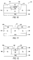
- FIG. 10 illustrates the finished memory cell 40 A
- FIGS. 4-9 illustrate the memory cell 40 A at various stages of fabrication.
- the suffix “A” is used in describing this first embodiment for clarity so that similar reference numerals may be used to describe subsequent embodiments.
- the finished memory cell 40 A includes a word line 42 A, which is often referred to as a Metal 1 (M1) layer.
- the word line 42 A has a layer of conductive material 50 A, such as silver (Ag), disposed thereon.
- a layer of chalcogenide material 52 A such as germanium selenide (GeSe), having metal ions diffused therein is disposed over the conductive layer 50 A.
- the metal ions diffused in the chalcogenide material 52 A typically originate in the layer of conductive material 50 A.
- the digit line 44 A often referred to as a Metal 2 (M2) layer, is disposed over the chalcogenide layer 52 A.
- M2 Metal 2
- Each memory cell 40 A is typically isolated from adjacent memory cells by oxide regions 54 A, and each memory cell 40 A is typically fabricated on a substrate 56 A.
- a substrate 56 A is typically used as a base upon which the memory cells 40 A of the memory array 44 are formed.
- the substrate 56 A is generally used in a generic sense, because it is possible for the substrate 56 A to take various forms depending upon the nature of the circuit design.
- the substrate 56 A may be a suitable semiconductor substrate, such as silicon or galium arsenide, or a suitable dielectric substrate, such as PECVD silicon dioxide.
- the substrate 56 A may include layers, devices, and/or structures upon which or around which the memory cells 40 A may be fabricated.
- a layer of dielectric material 54 A for example an oxide such as silicon dioxide, is formed over the substrate 56 A, as illustrated in FIG. 5 .
- the layer of dielectric material 54 A may be formed by any suitable process, such as by chemical vapor deposition.
- a window 58 A is formed in the layer of dielectric material 54 A. The window may extend partially through the layer of dielectric material 54 A, or completely through the layer of dielectric material 54 A to the substrate 56 A, as illustrated in FIG. 5 .
- the window 58 A may be formed by any suitable process, such as by the use of standard photolithographic techniques.
- a layer of conductive material is deposited into the window 58 A and planarized to form the word line 42 A.
- any suitable deposition technique such as sputtering, and any suitable planarization technique, such as chemical mechanical planarization (CMP), may be used.
- the conductive material used to form the word line 42 A is typically a metal, such as copper, tungsten, nickel, or aluminum.
- the word line 42 A is illustrated as being formed in a dielectric material 54 A in this embodiment, it should be appreciated that the word line 42 A may be formed in other manners as well. For example, the word line 42 A may be buried in the substrate 56 A.
- a fast ion conductive material is then disposed on the word line 42 A.
- the fast ion conductive material is selected to cooperate with a subsequently applied layer of chalcogenide material to form the memory element of the memory cell 40 A.
- the word line 42 A is plated with the conductive material 50 A using an immersion plating process.
- immersion plating replaces a less noble metal with a more noble metal. It is an ion exchange process that requires neither external electricity nor a catalyst.
- Immersion plating can be used in a self-limiting process, and it usually plates thinner films than other plating methods. Immersion plating depends on the base metal, i.e., the less noble metal. Many factors can influence immersion plating, such as the type of ligand used to take up the base metal and to keep the base metal in solution.
- the base metal of the word line 42 A is selected to be copper, and the more noble metal of the conductive layer 50 A is selected to be silver.
- the base metal of the word line 42 A is selected to be copper
- the more noble metal of the conductive layer 50 A is selected to be silver.
- other base metals such as nickel, aluminum, or tungsten, for example, may be used in place of copper, and that alloys of such metals may be used as well.
- various “more noble” metals, such as gold may be used in place of silver.
- a silver immersion solution called “argentomerse” available from Technic, Inc. may be used. This silver immersion solution utilizes a cyanide salt chemistry, which essentially represents a general purpose immersion plating solution.
- a silver immersion solution such as argentomerse should suffice for plating silver on base metals such as nickel or copper. However, for immersion plating of silver on tungsten, it may be desirable to utilize another silver immersion solution in order to optimize the chemistry.
- the structure illustrated in FIG. 6 is immersed in the silver immersion solution for a sufficient amount of time to form the layer of conductive material 50 A For example, the structure may be immersed in the solution for 15 to 30 minutes to form the conductive layer 5 A having a thickness of 500 A to 2000 A.
- a layer of chalcogenide material 52 A such as germanium selenide, may be formed over the conductive layer 50 A, as illustrated in FIG. 8 .
- the layer of chalcogenide material 52 A may be formed by any suitable process, such as chemical vapor deposition.
- the layer of chalcogenide material 52 A may have a thickness in the range of 200 A to 800 A, for example.
- the structure illustrated in FIG. 8 is processed in a manner that causes at least a portion of the material in the conductive layer 50 A to migrate into the layer of chalcogenide material 52 A.
- the structure illustrated in FIG. 8 is subjected to ultraviolet radiation and heat to cause silver atoms in the layer of conductive material 50 A to migrate into the layer of chalcogenide material 52 A.
- the structure in FIG. 8 is subjected to ultraviolet radiation and heat to cause silver atoms in the layer of conductive material 50 A to migrate into the layer of chalcogenide material 52 A.
- UV radiation 8 may be submitted to ultraviolet radiation in the range of 160 nm to 904 nm, e.g., 405 nm, at an intensity of 10 microjoules to 10 millijoules for a period of 5 to 30 minutes, and heat at a temperature of 50 to 85 degrees Celsius for a period of 5 to 20 minutes.
- the heat cycle is performed first, followed by the UV cycle.
- the layer of chalcogenide material 52 A has metal ions in it, as illustrated in FIG. 9 .
- the Metal 2 (M2) layer which forms the digit line 44 A, may be disposed over the layer of chalcogenide material 52 A, as illustrated in FIG. 10 , to complete the memory cell 40 A.
- the memory cell 40 A represents an inverted PCRAM memory cell.
- a typical PCRAM memory cell is fabricated by forming a layer of chalcogenide material on the Metal 1 layer, thus requiring the conductive layer, such as silver, to be disposed on the chalcogenide layer.
- chalcogenide is a very delicate material as discussed previously, known methods of depositing silver on chalcogenide are difficult to control in a reliable and repeatable fashion.
- the delicate nature of the subsequently deposited chalcogenide material does not pose a problem.
- FIGS. 11-15 illustrate a second embodiment of the memory cell 40 .
- FIG. 15 illustrates the finished memory cell 40 B
- FIGS. 11-14 illustrate the memory cell 40 B at various stages of fabrication.
- the suffix “B” is used in describing this second embodiment for clarity so that similar reference numerals may be used.
- the finished memory cell 40 B includes a word line 42 B, which is again referred to as a Metal 1 (M1) layer.
- the word line 42 B has a layer of conductive material 50 B, such as silver (Ag), disposed thereon.
- a layer of chalcogenide material 52 B, such as germanium selenide (GeSe), having metal ions diffused therein is disposed over the conductive layer 50 B.
- the layer of conductive material 50 B and the layer of chalcogenide material 52 B are disposed in a window created in a layer of dielectric material 60 B.
- the digit line 44 B again referred to as a Metal 2 (M2) layer, is disposed over the chalcogenide layer 52 B.
- M2 Metal 2
- Each memory cell 40 B is typically isolated from adjacent memory cells by oxide regions 54 B, and each memory cell 40 B is typically fabricated on a substrate 56 B.
- FIGS. 11-14 One method of fabricating the memory cell 40 B is disclosed with reference to, the various stages of fabrication illustrated in FIGS. 11-14 . However, before discussing FIGS. 11-14 , it should be understood that the memory cell 40 B first undergoes the stages of fabrication illustrated in FIGS. 4-6 . Then, as illustrated in FIG. 11 , a layer of dielectric material 60 B is deposited over the structure, and a window 62 is formed in the layer of dielectric material 60 B to expose at least a portion of the underlying word line 42 B.
- the layer of dielectric material 60 B may be deposited in any suitable manner, such as by chemical vapor deposition, and it may include any suitable dielectric, such as silicon nitride.
- the thickness of the layer of dielectric material 60 B may be in the range of 200 A to 1000 A, for example.
- a fast ion conductive material is then disposed on the portion of the word line 42 B exposed by the window 62 .
- the selection of the fast ion conductive material and the manner in which it may be applied does not differ from the previous embodiment. Accordingly, for the sake of clarity, in this exemplary embodiment, the base metal of the word line 42 B is selected to be copper, and the more noble metal of the conductive layer 50 B is selected to be silver.
- the structure illustrated in FIG. 11 is immersed in the silver immersion solution for a sufficient amount of time to form the layer of conductive material 50 B, as illustrated in FIG. 12 .
- a layer of chalcogenide material 52 B such as germanium selenide, may be deposited in the window 62 over the conductive layer 50 B, as illustrated in FIG. 13 .
- the layer of chalcogenide material 52 B may be formed by any suitable process, such as chemical vapor deposition.
- the deposited layer of chalcogenide material 52 B is then planarized, by chemical mechanical planarizatiqn for example, so that the layer of chalcogenide material 52 B remains only within the window 62 .
- the thickness of the layer of chalcogenide material 52 B is approximately the same as the thickness of the layer of dielectric material 60 B.
- the structure illustrated in FIG. 13 is processed in a manner that causes at least a portion of the material in the conductive layer 50 B to migrate into the layer of chalcogenide material 52 B.
- the structure illustrated in FIG. 13 is subjected to ultraviolet radiation and heat to cause silver atoms in the layer of conductive material 50 B to migrate into the layer of chalcogenide material 52 B.
- the layer of chalcogenide material 52 B has metal ions in it, as illustrated in FIG. 14 .
- the Metal 2 (M2) layer which forms the digit line 44 B, may be disposed over the layer of dielectric material 60 B and over the layer of chalcogenide material 52 B, as illustrated in FIG. 15 , to complete the memory cell 40 B.
- FIGS. 16-19 illustrate a third embodiment of the memory cell 40 .
- FIG. 19 illustrates the finished memory cell 40 C
- FIGS. 16-18 illustrate the memory cell 40 C at various stages of fabrication.
- the suffix “C” is used in describing this third embodiment for clarity so that similar reference numerals may be used.
- the finished memory cell 40 C includes a word line 42 C, which is again referred to as a Metal 1 (M1) layer.
- the word line 42 C has a layer of conductive material 50 C, such as silver (Ag), disposed thereon.
- a layer of chalcogenide material 52 C, such as germanium selenide (GeSe), having metal ions diffused therein is disposed over the conductive layer 50 C.
- the layer of conductive material 50 C and the layer of chalcogenide material 52 C are disposed in a window created in a layer of dielectric material 60 C and in a layer of conductive material 44 ′C.
- the layer of conductive material 44 ′C forms a portion of the digit line and is again referred to as a Metal 2 (M2) layer.
- the other portion of the digit line is formed by a layer of conductive material 44 ′′C, which is disposed over the chalcogenide layer 52 C and over the Metal 2 layer.
- the layer of conductive material 44 ′′C is referred to as the Metal 3 (M3) layer.
- Each memory cell 40 C is typically isolated from adjacent memory cells by oxide regions 54 C, and each memory cell 40 C is typically fabricated on a substrate 56 C.
- FIGS. 16-18 One method of fabricating the memory cell 40 C is disclosed with reference to the various stages of fabrication illustrated in FIGS. 16-18 . However, before discussing FIGS. 16-18 , it should be understood that the memory cell 40 C first undergoes the stages of fabrication illustrated in FIGS. 4-6 . Then, as illustrated in FIG. 16 , a layer of dielectric material 60 C is deposited over the structure, and a layer of conductive material 44 ′C (the Metal 2 layer) is deposited over the layer of dielectric material 60 C.
- the layer of dielectric material 60 C may be deposited in any suitable manner, such as by chemical vapor deposition, and it may include any suitable dielectric, such as silicon nitride.
- the layer of conductive material 44 ′C may be deposited in any suitable manner, such as by sputtering, and it may include any suitable conductive material, such as platinum, aluminum, or tungsten.
- the thickness of the layer of dielectric material 60 C may be in the range of 200 A to 1000 A, for example, and the thickness of the layer of conductive material 44 ′C may be in the range of 500 A to 2000 A, for example.
- a window 64 is formed in the layer of dielectric material 60 C and in the layer of conductive material 44 ′C to expose at least a portion of the underlying word line 42 C.
- the window 64 may be formed in any suitable manner, such as by the use of standard photolithographic techniques.
- a fast ion conductive material is then disposed on the portion of the word line 42 C exposed by the window 64 .
- the selection of the fast ion conductive material and the manner in which it may be applied does not differ from the previous embodiments. Accordingly, for the sake of clarity, in this exemplary embodiment, the base metal of the word line 42 C is selected to be copper, and the more noble metal of the conductive layer 50 C is selected to be silver.
- the structure illustrated in FIG. 16 is immersed in the silver immersion solution for a sufficient amount of time to form the layer of conductive material 50 C, as illustrated in FIG. 17 .
- a layer of chalcogenide material 52 C such as germanium selenide, may be deposited in the window 64 over the conductive layer 50 C, as illustrated in FIG. 18 .
- the layer of chalcogenide material 52 C may be formed by any suitable process, such as chemical vapor deposition.
- the deposited layer of chalcogenide material 52 C is then planarized, by chemical mechanical planarization for example, so that the layer of chalcogenide material 52 C remains only within the window 64 .
- the thickness of the layer of chalcogenide material 52 C is approximately the same as the thickness of the layers of dielectric material 60 C and conductive material 44 ′C.
- the structure illustrated in FIG. 18 is processed in a manner that causes at least a portion of the material in the conductive layer 50 C to migrate into the layer of chalcogenide material 52 C.
- the structure illustrated in FIG. 18 is subjected to ultraviolet radiation and heat to cause silver atoms in the layer of conductive material 50 C to migrate into the layer of chalcogenide material 52 C.
- the layer of chalcogenide material 52 C has metal ions in it, as illustrated in FIG. 19 .
- a layer of conductive material 44 ′′C (the Metal 3 layer), which forms the remainder of the digit line, may be disposed over the layer of conductive material 44 ′C and over the layer of chalcogenide material 52 C to complete the memory cell 40 C.
- chalcogenide material is somewhat susceptible to damage from planarization techniques, such as chemical mechanical planarization.
- planarization techniques such as chemical mechanical planarization.
- the memory cell 40 C is relatively immune to any “over planarization” of the chalcogenide material 52 C within the window 64 .
- the planarization step can remove some of the relatively delicate chalcogenide material 52 C from the top of the window 64 , the electrical path from the digit line 44 C through the chalcogenide material 52 C typically does not extend directly from the layer of conductive material 44 ′′C. Rather, the shortest path typically extends from the edge of the layer of conductive material 44 ′C.
- the memory cell 40 C typically provides for relatively repeatable and consistent memory operation.
Landscapes
- Engineering & Computer Science (AREA)
- Manufacturing & Machinery (AREA)
- Physics & Mathematics (AREA)
- Condensed Matter Physics & Semiconductors (AREA)
- General Physics & Mathematics (AREA)
- Computer Hardware Design (AREA)
- Microelectronics & Electronic Packaging (AREA)
- Power Engineering (AREA)
- Semiconductor Memories (AREA)
Abstract
Description
Claims (16)
Priority Applications (1)
| Application Number | Priority Date | Filing Date | Title |
|---|---|---|---|
| US11/751,896 US7687793B2 (en) | 2001-05-11 | 2007-05-22 | Resistance variable memory cells |
Applications Claiming Priority (4)
| Application Number | Priority Date | Filing Date | Title |
|---|---|---|---|
| US09/853,233 US7102150B2 (en) | 2001-05-11 | 2001-05-11 | PCRAM memory cell and method of making same |
| US10/205,387 US7071021B2 (en) | 2001-05-11 | 2002-07-25 | PCRAM memory cell and method of making same |
| US11/302,119 US7235419B2 (en) | 2001-05-11 | 2005-12-14 | Method of making a memory cell |
| US11/751,896 US7687793B2 (en) | 2001-05-11 | 2007-05-22 | Resistance variable memory cells |
Related Parent Applications (1)
| Application Number | Title | Priority Date | Filing Date |
|---|---|---|---|
| US11/302,119 Continuation US7235419B2 (en) | 2001-05-11 | 2005-12-14 | Method of making a memory cell |
Publications (2)
| Publication Number | Publication Date |
|---|---|
| US20070235712A1 US20070235712A1 (en) | 2007-10-11 |
| US7687793B2 true US7687793B2 (en) | 2010-03-30 |
Family
ID=25315450
Family Applications (4)
| Application Number | Title | Priority Date | Filing Date |
|---|---|---|---|
| US09/853,233 Expired - Lifetime US7102150B2 (en) | 2001-05-11 | 2001-05-11 | PCRAM memory cell and method of making same |
| US10/205,387 Expired - Fee Related US7071021B2 (en) | 2001-05-11 | 2002-07-25 | PCRAM memory cell and method of making same |
| US11/302,119 Expired - Lifetime US7235419B2 (en) | 2001-05-11 | 2005-12-14 | Method of making a memory cell |
| US11/751,896 Expired - Fee Related US7687793B2 (en) | 2001-05-11 | 2007-05-22 | Resistance variable memory cells |
Family Applications Before (3)
| Application Number | Title | Priority Date | Filing Date |
|---|---|---|---|
| US09/853,233 Expired - Lifetime US7102150B2 (en) | 2001-05-11 | 2001-05-11 | PCRAM memory cell and method of making same |
| US10/205,387 Expired - Fee Related US7071021B2 (en) | 2001-05-11 | 2002-07-25 | PCRAM memory cell and method of making same |
| US11/302,119 Expired - Lifetime US7235419B2 (en) | 2001-05-11 | 2005-12-14 | Method of making a memory cell |
Country Status (1)
| Country | Link |
|---|---|
| US (4) | US7102150B2 (en) |
Cited By (21)
| Publication number | Priority date | Publication date | Assignee | Title |
|---|---|---|---|---|
| US20050226062A1 (en) * | 2003-03-20 | 2005-10-13 | Sony Corporation | Memory element and storage device using this |
| US20090250681A1 (en) * | 2008-04-08 | 2009-10-08 | John Smythe | Non-Volatile Resistive Oxide Memory Cells, Non-Volatile Resistive Oxide Memory Arrays, And Methods Of Forming Non-Volatile Resistive Oxide Memory Cells And Memory Arrays |
| US20090272960A1 (en) * | 2008-05-02 | 2009-11-05 | Bhaskar Srinivasan | Non-Volatile Resistive Oxide Memory Cells, and Methods Of Forming Non-Volatile Resistive Oxide Memory Cells |
| US20090317540A1 (en) * | 2008-06-18 | 2009-12-24 | Gurtej Sandhu | Methods Of Forming A Non-Volatile Resistive Oxide Memory Array |
| US20090316467A1 (en) * | 2008-06-18 | 2009-12-24 | Jun Liu | Memory Device Constructions, Memory Cell Forming Methods, and Semiconductor Construction Forming Methods |
| US20100003782A1 (en) * | 2008-07-02 | 2010-01-07 | Nishant Sinha | Methods Of Forming A Non-Volatile Resistive Oxide Memory Cell And Methods Of Forming A Non-Volatile Resistive Oxide Memory Array |
| US20100271863A1 (en) * | 2008-01-15 | 2010-10-28 | Jun Liu | Memory Cells, Memory Cell Programming Methods, Memory Cell Reading Methods, Memory Cell Operating Methods, and Memory Devices |
| WO2012060993A3 (en) * | 2010-11-01 | 2012-07-05 | Micron Technology, Inc. | Methods of forming electrical components and memory cells |
| US8411477B2 (en) | 2010-04-22 | 2013-04-02 | Micron Technology, Inc. | Arrays of vertically stacked tiers of non-volatile cross point memory cells, methods of forming arrays of vertically stacked tiers of non-volatile cross point memory cells, and methods of reading a data value stored by an array of vertically stacked tiers of non-volatile cross point memory cells |
| US8427859B2 (en) | 2010-04-22 | 2013-04-23 | Micron Technology, Inc. | Arrays of vertically stacked tiers of non-volatile cross point memory cells, methods of forming arrays of vertically stacked tiers of non-volatile cross point memory cells, and methods of reading a data value stored by an array of vertically stacked tiers of non-volatile cross point memory cells |
| US8431458B2 (en) | 2010-12-27 | 2013-04-30 | Micron Technology, Inc. | Methods of forming a nonvolatile memory cell and methods of forming an array of nonvolatile memory cells |
| US8537592B2 (en) | 2011-04-15 | 2013-09-17 | Micron Technology, Inc. | Arrays of nonvolatile memory cells and methods of forming arrays of nonvolatile memory cells |
| US8681531B2 (en) | 2011-02-24 | 2014-03-25 | Micron Technology, Inc. | Memory cells, methods of forming memory cells, and methods of programming memory cells |
| US8753949B2 (en) | 2010-11-01 | 2014-06-17 | Micron Technology, Inc. | Nonvolatile memory cells and methods of forming nonvolatile memory cells |
| US8759809B2 (en) | 2010-10-21 | 2014-06-24 | Micron Technology, Inc. | Integrated circuitry comprising nonvolatile memory cells having platelike electrode and ion conductive material layer |
| US8791447B2 (en) | 2011-01-20 | 2014-07-29 | Micron Technology, Inc. | Arrays of nonvolatile memory cells and methods of forming arrays of nonvolatile memory cells |
| US8811063B2 (en) | 2010-11-01 | 2014-08-19 | Micron Technology, Inc. | Memory cells, methods of programming memory cells, and methods of forming memory cells |
| US8962460B2 (en) | 2011-04-26 | 2015-02-24 | Micron Technology, Inc. | Methods of selectively forming metal-doped chalcogenide materials, methods of selectively doping chalcogenide materials, and methods of forming semiconductor device structures including same |
| US8976566B2 (en) | 2010-09-29 | 2015-03-10 | Micron Technology, Inc. | Electronic devices, memory devices and memory arrays |
| US9412421B2 (en) | 2010-06-07 | 2016-08-09 | Micron Technology, Inc. | Memory arrays |
| US9454997B2 (en) | 2010-12-02 | 2016-09-27 | Micron Technology, Inc. | Array of nonvolatile memory cells having at least five memory cells per unit cell, having a plurality of the unit cells which individually comprise three elevational regions of programmable material, and/or having a continuous volume having a combination of a plurality of vertically oriented memory cells and a plurality of horizontally oriented memory cells; array of vertically stacked tiers of nonvolatile memory cells |
Families Citing this family (161)
| Publication number | Priority date | Publication date | Assignee | Title |
|---|---|---|---|---|
| US5841768A (en) | 1996-06-27 | 1998-11-24 | Interdigital Technology Corporation | Method of controlling initial power ramp-up in CDMA systems by using short codes |
| US7902536B2 (en) * | 1999-03-25 | 2011-03-08 | Ovonyx, Inc. | Memory device and method of making same |
| US7102150B2 (en) * | 2001-05-11 | 2006-09-05 | Harshfield Steven T | PCRAM memory cell and method of making same |
| US6955940B2 (en) | 2001-08-29 | 2005-10-18 | Micron Technology, Inc. | Method of forming chalcogenide comprising devices |
| US6881623B2 (en) * | 2001-08-29 | 2005-04-19 | Micron Technology, Inc. | Method of forming chalcogenide comprising devices, method of forming a programmable memory cell of memory circuitry, and a chalcogenide comprising device |
| US6646902B2 (en) | 2001-08-30 | 2003-11-11 | Micron Technology, Inc. | Method of retaining memory state in a programmable conductor RAM |
| US6800899B2 (en) * | 2001-08-30 | 2004-10-05 | Micron Technology, Inc. | Vertical transistors, electrical devices containing a vertical transistor, and computer systems containing a vertical transistor |
| US7109056B2 (en) * | 2001-09-20 | 2006-09-19 | Micron Technology, Inc. | Electro-and electroless plating of metal in the manufacture of PCRAM devices |
| US6791859B2 (en) | 2001-11-20 | 2004-09-14 | Micron Technology, Inc. | Complementary bit PCRAM sense amplifier and method of operation |
| US6909656B2 (en) * | 2002-01-04 | 2005-06-21 | Micron Technology, Inc. | PCRAM rewrite prevention |
| US6791885B2 (en) | 2002-02-19 | 2004-09-14 | Micron Technology, Inc. | Programmable conductor random access memory and method for sensing same |
| US6847535B2 (en) | 2002-02-20 | 2005-01-25 | Micron Technology, Inc. | Removable programmable conductor memory card and associated read/write device and method of operation |
| US7151273B2 (en) | 2002-02-20 | 2006-12-19 | Micron Technology, Inc. | Silver-selenide/chalcogenide glass stack for resistance variable memory |
| US6849868B2 (en) | 2002-03-14 | 2005-02-01 | Micron Technology, Inc. | Methods and apparatus for resistance variable material cells |
| US6864500B2 (en) | 2002-04-10 | 2005-03-08 | Micron Technology, Inc. | Programmable conductor memory cell structure |
| US6731528B2 (en) * | 2002-05-03 | 2004-05-04 | Micron Technology, Inc. | Dual write cycle programmable conductor memory system and method of operation |
| US6825135B2 (en) | 2002-06-06 | 2004-11-30 | Micron Technology, Inc. | Elimination of dendrite formation during metal/chalcogenide glass deposition |
| US6890790B2 (en) | 2002-06-06 | 2005-05-10 | Micron Technology, Inc. | Co-sputter deposition of metal-doped chalcogenides |
| TWI233204B (en) * | 2002-07-26 | 2005-05-21 | Infineon Technologies Ag | Nonvolatile memory element and associated production methods and memory element arrangements |
| US7018863B2 (en) * | 2002-08-22 | 2006-03-28 | Micron Technology, Inc. | Method of manufacture of a resistance variable memory cell |
| US7010644B2 (en) | 2002-08-29 | 2006-03-07 | Micron Technology, Inc. | Software refreshed memory device and method |
| US7364644B2 (en) | 2002-08-29 | 2008-04-29 | Micron Technology, Inc. | Silver selenide film stoichiometry and morphology control in sputter deposition |
| US6864521B2 (en) | 2002-08-29 | 2005-03-08 | Micron Technology, Inc. | Method to control silver concentration in a resistance variable memory element |
| US7022579B2 (en) | 2003-03-14 | 2006-04-04 | Micron Technology, Inc. | Method for filling via with metal |
| DE10342026A1 (en) * | 2003-09-11 | 2005-04-28 | Infineon Technologies Ag | Memory cell with ion conduction storage mechanism and method for its production |
| US7050319B2 (en) * | 2003-12-03 | 2006-05-23 | Micron Technology, Inc. | Memory architecture and method of manufacture and operation thereof |
| KR100533958B1 (en) * | 2004-01-05 | 2005-12-06 | 삼성전자주식회사 | Phase-change memory device and method of manufacturing the same |
| US7138687B2 (en) * | 2004-01-26 | 2006-11-21 | Macronix International Co., Ltd. | Thin film phase-change memory |
| US7583551B2 (en) | 2004-03-10 | 2009-09-01 | Micron Technology, Inc. | Power management control and controlling memory refresh operations |
| US20050260338A1 (en) * | 2004-05-19 | 2005-11-24 | Trendon Touch Technology Corp. | Method of manufacturing circuit layout on touch panel by utilizing metal plating technology |
| US7326950B2 (en) | 2004-07-19 | 2008-02-05 | Micron Technology, Inc. | Memory device with switching glass layer |
| US7354793B2 (en) | 2004-08-12 | 2008-04-08 | Micron Technology, Inc. | Method of forming a PCRAM device incorporating a resistance-variable chalocogenide element |
| US7365411B2 (en) | 2004-08-12 | 2008-04-29 | Micron Technology, Inc. | Resistance variable memory with temperature tolerant materials |
| US7224598B2 (en) * | 2004-09-02 | 2007-05-29 | Hewlett-Packard Development Company, L.P. | Programming of programmable resistive memory devices |
| US7189626B2 (en) * | 2004-11-03 | 2007-03-13 | Micron Technology, Inc. | Electroless plating of metal caps for chalcogenide-based memory devices |
| US20060131555A1 (en) * | 2004-12-22 | 2006-06-22 | Micron Technology, Inc. | Resistance variable devices with controllable channels |
| US7374174B2 (en) | 2004-12-22 | 2008-05-20 | Micron Technology, Inc. | Small electrode for resistance variable devices |
| FR2880177B1 (en) * | 2004-12-23 | 2007-05-18 | Commissariat Energie Atomique | MEMORY PMC HAVING IMPROVED RETENTION TIME AND WRITING SPEED |
| US7361925B2 (en) * | 2005-02-10 | 2008-04-22 | Infineon Technologies Ag | Integrated circuit having a memory including a low-k dielectric material for thermal isolation |
| US7317200B2 (en) | 2005-02-23 | 2008-01-08 | Micron Technology, Inc. | SnSe-based limited reprogrammable cell |
| DE102005012047A1 (en) * | 2005-03-16 | 2006-09-28 | Infineon Technologies Ag | Solid-state electrolyte memory manufacture involves coating first electrode with solid-state electrolyte layer, and then forming second electrode on solid-state electrolyte layer |
| US7709289B2 (en) | 2005-04-22 | 2010-05-04 | Micron Technology, Inc. | Memory elements having patterned electrodes and method of forming the same |
| US7427770B2 (en) | 2005-04-22 | 2008-09-23 | Micron Technology, Inc. | Memory array for increased bit density |
| US7274034B2 (en) | 2005-08-01 | 2007-09-25 | Micron Technology, Inc. | Resistance variable memory device with sputtered metal-chalcogenide region and method of fabrication |
| US7332735B2 (en) | 2005-08-02 | 2008-02-19 | Micron Technology, Inc. | Phase change memory cell and method of formation |
| US7579615B2 (en) | 2005-08-09 | 2009-08-25 | Micron Technology, Inc. | Access transistor for memory device |
| US7251154B2 (en) | 2005-08-15 | 2007-07-31 | Micron Technology, Inc. | Method and apparatus providing a cross-point memory array using a variable resistance memory cell and capacitance |
| US7635855B2 (en) | 2005-11-15 | 2009-12-22 | Macronix International Co., Ltd. | I-shaped phase change memory cell |
| US7449710B2 (en) | 2005-11-21 | 2008-11-11 | Macronix International Co., Ltd. | Vacuum jacket for phase change memory element |
| US7875871B2 (en) | 2006-03-31 | 2011-01-25 | Sandisk 3D Llc | Heterojunction device comprising a semiconductor and a resistivity-switching oxide or nitride |
| KR100729361B1 (en) * | 2006-04-24 | 2007-06-15 | 삼성전자주식회사 | Gap fill method and method for forming semiconductor memory device using the same |
| US7501648B2 (en) * | 2006-08-16 | 2009-03-10 | International Business Machines Corporation | Phase change materials and associated memory devices |
| US7560723B2 (en) | 2006-08-29 | 2009-07-14 | Micron Technology, Inc. | Enhanced memory density resistance variable memory cells, arrays, devices and systems including the same, and methods of fabrication |
| US8003972B2 (en) | 2006-08-30 | 2011-08-23 | Micron Technology, Inc. | Bottom electrode geometry for phase change memory |
| US7511984B2 (en) * | 2006-08-30 | 2009-03-31 | Micron Technology, Inc. | Phase change memory |
| US8232175B2 (en) * | 2006-09-14 | 2012-07-31 | Spansion Llc | Damascene metal-insulator-metal (MIM) device with improved scaleability |
| WO2008088599A2 (en) * | 2006-10-19 | 2008-07-24 | Boise State University | Forced ion migration for chalcogenide phase change memory device |
| US7718989B2 (en) | 2006-12-28 | 2010-05-18 | Macronix International Co., Ltd. | Resistor random access memory cell device |
| US7663135B2 (en) * | 2007-01-31 | 2010-02-16 | Macronix International Co., Ltd. | Memory cell having a side electrode contact |
| US7800093B2 (en) * | 2007-02-01 | 2010-09-21 | Qimonda North America Corp. | Resistive memory including buried word lines |
| US7718533B2 (en) * | 2007-05-08 | 2010-05-18 | Micron Technology, Inc. | Inverted variable resistance memory cell and method of making the same |
| US20080278988A1 (en) * | 2007-05-09 | 2008-11-13 | Klaus Ufert | Resistive switching element |
| KR100881055B1 (en) * | 2007-06-20 | 2009-01-30 | 삼성전자주식회사 | Phase-change memory unit, method of forming the phase-change memory unit, phase-change memory device having the phase-change memory unit and method of manufacturing the phase-change memory device |
| US7813167B2 (en) * | 2008-03-21 | 2010-10-12 | Micron Technology, Inc. | Memory cell |
| US8233308B2 (en) | 2007-06-29 | 2012-07-31 | Sandisk 3D Llc | Memory cell that employs a selectively deposited reversible resistance-switching element and methods of forming the same |
| CN101720506B (en) * | 2007-06-29 | 2012-05-16 | 桑迪士克3D公司 | Memory cell that employs a selectively deposited reversible resistance-switching element and methods of forming the same |
| US7824956B2 (en) | 2007-06-29 | 2010-11-02 | Sandisk 3D Llc | Memory cell that employs a selectively grown reversible resistance-switching element and methods of forming the same |
| US20090104756A1 (en) * | 2007-06-29 | 2009-04-23 | Tanmay Kumar | Method to form a rewriteable memory cell comprising a diode and a resistivity-switching grown oxide |
| US7884342B2 (en) * | 2007-07-31 | 2011-02-08 | Macronix International Co., Ltd. | Phase change memory bridge cell |
| US7729161B2 (en) * | 2007-08-02 | 2010-06-01 | Macronix International Co., Ltd. | Phase change memory with dual word lines and source lines and method of operating same |
| FR2922368A1 (en) * | 2007-10-16 | 2009-04-17 | Commissariat Energie Atomique | METHOD FOR MANUFACTURING A CBRAM MEMORY HAVING IMPROVED RELIABILITY |
| US7989793B2 (en) * | 2007-12-10 | 2011-08-02 | Electronics And Telecommunications Research Institute | Electrical device using phase change material, phase change memory device using solid state reaction and method for fabricating the same |
| US8168468B2 (en) * | 2008-02-29 | 2012-05-01 | Freescale Semiconductor, Inc. | Method of making a semiconductor device including a bridgeable material |
| US7491573B1 (en) | 2008-03-13 | 2009-02-17 | International Business Machines Corporation | Phase change materials for applications that require fast switching and high endurance |
| US8467236B2 (en) | 2008-08-01 | 2013-06-18 | Boise State University | Continuously variable resistor |
| US7825479B2 (en) * | 2008-08-06 | 2010-11-02 | International Business Machines Corporation | Electrical antifuse having a multi-thickness dielectric layer |
| US8064247B2 (en) * | 2009-01-14 | 2011-11-22 | Macronix International Co., Ltd. | Rewritable memory device based on segregation/re-absorption |
| US8809829B2 (en) | 2009-06-15 | 2014-08-19 | Macronix International Co., Ltd. | Phase change memory having stabilized microstructure and manufacturing method |
| US8406033B2 (en) * | 2009-06-22 | 2013-03-26 | Macronix International Co., Ltd. | Memory device and method for sensing and fixing margin cells |
| US8238149B2 (en) * | 2009-06-25 | 2012-08-07 | Macronix International Co., Ltd. | Methods and apparatus for reducing defect bits in phase change memory |
| US8363463B2 (en) * | 2009-06-25 | 2013-01-29 | Macronix International Co., Ltd. | Phase change memory having one or more non-constant doping profiles |
| US8198619B2 (en) | 2009-07-15 | 2012-06-12 | Macronix International Co., Ltd. | Phase change memory cell structure |
| US7894254B2 (en) * | 2009-07-15 | 2011-02-22 | Macronix International Co., Ltd. | Refresh circuitry for phase change memory |
| US8110822B2 (en) * | 2009-07-15 | 2012-02-07 | Macronix International Co., Ltd. | Thermal protect PCRAM structure and methods for making |
| US20110049456A1 (en) * | 2009-09-03 | 2011-03-03 | Macronix International Co., Ltd. | Phase change structure with composite doping for phase change memory |
| US8064248B2 (en) * | 2009-09-17 | 2011-11-22 | Macronix International Co., Ltd. | 2T2R-1T1R mix mode phase change memory array |
| US8178387B2 (en) * | 2009-10-23 | 2012-05-15 | Macronix International Co., Ltd. | Methods for reducing recrystallization time for a phase change material |
| US8729521B2 (en) | 2010-05-12 | 2014-05-20 | Macronix International Co., Ltd. | Self aligned fin-type programmable memory cell |
| US9012307B2 (en) | 2010-07-13 | 2015-04-21 | Crossbar, Inc. | Two terminal resistive switching device structure and method of fabricating |
| US9570678B1 (en) | 2010-06-08 | 2017-02-14 | Crossbar, Inc. | Resistive RAM with preferental filament formation region and methods |
| US9601692B1 (en) | 2010-07-13 | 2017-03-21 | Crossbar, Inc. | Hetero-switching layer in a RRAM device and method |
| US8946046B1 (en) | 2012-05-02 | 2015-02-03 | Crossbar, Inc. | Guided path for forming a conductive filament in RRAM |
| US8441835B2 (en) | 2010-06-11 | 2013-05-14 | Crossbar, Inc. | Interface control for improved switching in RRAM |
| WO2011156787A2 (en) * | 2010-06-11 | 2011-12-15 | Crossbar, Inc. | Pillar structure for memory device and method |
| US8310864B2 (en) | 2010-06-15 | 2012-11-13 | Macronix International Co., Ltd. | Self-aligned bit line under word line memory array |
| US8374018B2 (en) | 2010-07-09 | 2013-02-12 | Crossbar, Inc. | Resistive memory using SiGe material |
| US8168506B2 (en) | 2010-07-13 | 2012-05-01 | Crossbar, Inc. | On/off ratio for non-volatile memory device and method |
| US8884261B2 (en) | 2010-08-23 | 2014-11-11 | Crossbar, Inc. | Device switching using layered device structure |
| US8569172B1 (en) | 2012-08-14 | 2013-10-29 | Crossbar, Inc. | Noble metal/non-noble metal electrode for RRAM applications |
| US8467227B1 (en) | 2010-11-04 | 2013-06-18 | Crossbar, Inc. | Hetero resistive switching material layer in RRAM device and method |
| US8947908B2 (en) | 2010-11-04 | 2015-02-03 | Crossbar, Inc. | Hetero-switching layer in a RRAM device and method |
| US8394667B2 (en) * | 2010-07-14 | 2013-03-12 | Micron Technology, Inc. | Methods of forming memory cells, and methods of patterning chalcogenide-containing stacks |
| US8404553B2 (en) | 2010-08-23 | 2013-03-26 | Crossbar, Inc. | Disturb-resistant non-volatile memory device and method |
| US9401475B1 (en) | 2010-08-23 | 2016-07-26 | Crossbar, Inc. | Method for silver deposition for a non-volatile memory device |
| US8889521B1 (en) | 2012-09-14 | 2014-11-18 | Crossbar, Inc. | Method for silver deposition for a non-volatile memory device |
| US8492195B2 (en) | 2010-08-23 | 2013-07-23 | Crossbar, Inc. | Method for forming stackable non-volatile resistive switching memory devices |
| US8558212B2 (en) | 2010-09-29 | 2013-10-15 | Crossbar, Inc. | Conductive path in switching material in a resistive random access memory device and control |
| US8391049B2 (en) | 2010-09-29 | 2013-03-05 | Crossbar, Inc. | Resistor structure for a non-volatile memory device and method |
| US8395935B2 (en) | 2010-10-06 | 2013-03-12 | Macronix International Co., Ltd. | Cross-point self-aligned reduced cell size phase change memory |
| USRE46335E1 (en) | 2010-11-04 | 2017-03-07 | Crossbar, Inc. | Switching device having a non-linear element |
| US8502185B2 (en) | 2011-05-31 | 2013-08-06 | Crossbar, Inc. | Switching device having a non-linear element |
| US8088688B1 (en) | 2010-11-05 | 2012-01-03 | Crossbar, Inc. | p+ polysilicon material on aluminum for non-volatile memory device and method |
| US8497705B2 (en) | 2010-11-09 | 2013-07-30 | Macronix International Co., Ltd. | Phase change device for interconnection of programmable logic device |
| US8467238B2 (en) | 2010-11-15 | 2013-06-18 | Macronix International Co., Ltd. | Dynamic pulse operation for phase change memory |
| US8930174B2 (en) | 2010-12-28 | 2015-01-06 | Crossbar, Inc. | Modeling technique for resistive random access memory (RRAM) cells |
| US8791010B1 (en) | 2010-12-31 | 2014-07-29 | Crossbar, Inc. | Silver interconnects for stacked non-volatile memory device and method |
| US8815696B1 (en) | 2010-12-31 | 2014-08-26 | Crossbar, Inc. | Disturb-resistant non-volatile memory device using via-fill and etchback technique |
| US9153623B1 (en) | 2010-12-31 | 2015-10-06 | Crossbar, Inc. | Thin film transistor steering element for a non-volatile memory device |
| FR2972568B1 (en) * | 2011-03-09 | 2018-01-12 | Commissariat A L'energie Atomique Et Aux Energies Alternatives | ELECTRONIC DEVICE OF MEMORY TYPE |
| US8450710B2 (en) | 2011-05-27 | 2013-05-28 | Crossbar, Inc. | Low temperature p+ silicon junction material for a non-volatile memory device |
| US9620206B2 (en) | 2011-05-31 | 2017-04-11 | Crossbar, Inc. | Memory array architecture with two-terminal memory cells |
| US8394670B2 (en) | 2011-05-31 | 2013-03-12 | Crossbar, Inc. | Vertical diodes for non-volatile memory device |
| US8619459B1 (en) | 2011-06-23 | 2013-12-31 | Crossbar, Inc. | High operating speed resistive random access memory |
| US8946669B1 (en) | 2012-04-05 | 2015-02-03 | Crossbar, Inc. | Resistive memory device and fabrication methods |
| US9627443B2 (en) | 2011-06-30 | 2017-04-18 | Crossbar, Inc. | Three-dimensional oblique two-terminal memory with enhanced electric field |
| US8659929B2 (en) | 2011-06-30 | 2014-02-25 | Crossbar, Inc. | Amorphous silicon RRAM with non-linear device and operation |
| US9564587B1 (en) | 2011-06-30 | 2017-02-07 | Crossbar, Inc. | Three-dimensional two-terminal memory with enhanced electric field and segmented interconnects |
| US9166163B2 (en) | 2011-06-30 | 2015-10-20 | Crossbar, Inc. | Sub-oxide interface layer for two-terminal memory |
| CN103828047A (en) | 2011-07-22 | 2014-05-28 | 科洛斯巴股份有限公司 | Seed layer for a p + silicon germanium material for non-volatile memory device and method |
| US8648326B2 (en) * | 2011-07-27 | 2014-02-11 | International Business Machines Corporation | Phase change memory electrode with sheath for reduced programming current |
| US10056907B1 (en) | 2011-07-29 | 2018-08-21 | Crossbar, Inc. | Field programmable gate array utilizing two-terminal non-volatile memory |
| US8674724B2 (en) | 2011-07-29 | 2014-03-18 | Crossbar, Inc. | Field programmable gate array utilizing two-terminal non-volatile memory |
| US9729155B2 (en) | 2011-07-29 | 2017-08-08 | Crossbar, Inc. | Field programmable gate array utilizing two-terminal non-volatile memory |
| JP5840505B2 (en) * | 2012-01-12 | 2016-01-06 | 株式会社東芝 | Manufacturing method of semiconductor device |
| US9117515B2 (en) * | 2012-01-18 | 2015-08-25 | Macronix International Co., Ltd. | Programmable metallization cell with two dielectric layers |
| US8716098B1 (en) | 2012-03-09 | 2014-05-06 | Crossbar, Inc. | Selective removal method and structure of silver in resistive switching device for a non-volatile memory device |
| US9087576B1 (en) | 2012-03-29 | 2015-07-21 | Crossbar, Inc. | Low temperature fabrication method for a three-dimensional memory device and structure |
| US9685608B2 (en) | 2012-04-13 | 2017-06-20 | Crossbar, Inc. | Reduced diffusion in metal electrode for two-terminal memory |
| US8658476B1 (en) * | 2012-04-20 | 2014-02-25 | Crossbar, Inc. | Low temperature P+ polycrystalline silicon material for non-volatile memory device |
| US8796658B1 (en) | 2012-05-07 | 2014-08-05 | Crossbar, Inc. | Filamentary based non-volatile resistive memory device and method |
| US8853713B2 (en) | 2012-05-07 | 2014-10-07 | Micron Technology, Inc. | Resistive memory having confined filament formation |
| US8765566B2 (en) | 2012-05-10 | 2014-07-01 | Crossbar, Inc. | Line and space architecture for a non-volatile memory device |
| US9583701B1 (en) | 2012-08-14 | 2017-02-28 | Crossbar, Inc. | Methods for fabricating resistive memory device switching material using ion implantation |
| US10096653B2 (en) | 2012-08-14 | 2018-10-09 | Crossbar, Inc. | Monolithically integrated resistive memory using integrated-circuit foundry compatible processes |
| US8946673B1 (en) | 2012-08-24 | 2015-02-03 | Crossbar, Inc. | Resistive switching device structure with improved data retention for non-volatile memory device and method |
| US9312483B2 (en) | 2012-09-24 | 2016-04-12 | Crossbar, Inc. | Electrode structure for a non-volatile memory device and method |
| US9576616B2 (en) | 2012-10-10 | 2017-02-21 | Crossbar, Inc. | Non-volatile memory with overwrite capability and low write amplification |
| US11068620B2 (en) | 2012-11-09 | 2021-07-20 | Crossbar, Inc. | Secure circuit integrated with memory layer |
| US9437266B2 (en) | 2012-11-13 | 2016-09-06 | Macronix International Co., Ltd. | Unipolar programmable metallization cell |
| US8982647B2 (en) | 2012-11-14 | 2015-03-17 | Crossbar, Inc. | Resistive random access memory equalization and sensing |
| US9412790B1 (en) | 2012-12-04 | 2016-08-09 | Crossbar, Inc. | Scalable RRAM device architecture for a non-volatile memory device and method |
| US9406379B2 (en) | 2013-01-03 | 2016-08-02 | Crossbar, Inc. | Resistive random access memory with non-linear current-voltage relationship |
| US9112145B1 (en) | 2013-01-31 | 2015-08-18 | Crossbar, Inc. | Rectified switching of two-terminal memory via real time filament formation |
| US9324942B1 (en) | 2013-01-31 | 2016-04-26 | Crossbar, Inc. | Resistive memory cell with solid state diode |
| US8934280B1 (en) | 2013-02-06 | 2015-01-13 | Crossbar, Inc. | Capacitive discharge programming for two-terminal memory cells |
| US9093635B2 (en) | 2013-03-14 | 2015-07-28 | Crossbar, Inc. | Controlling on-state current for two-terminal memory |
| US10290801B2 (en) | 2014-02-07 | 2019-05-14 | Crossbar, Inc. | Scalable silicon based resistive memory device |
| US9672906B2 (en) | 2015-06-19 | 2017-06-06 | Macronix International Co., Ltd. | Phase change memory with inter-granular switching |
| US10062845B1 (en) * | 2016-05-13 | 2018-08-28 | Crossbar, Inc. | Flatness of memory cell surfaces |
| US10522754B2 (en) | 2016-06-15 | 2019-12-31 | Crossbar, Inc. | Liner layer for dielectric block layer |
| US10749110B1 (en) | 2016-07-15 | 2020-08-18 | Crossbar, Inc. | Memory stack liner comprising dielectric block layer material |
Citations (181)
| Publication number | Priority date | Publication date | Assignee | Title |
|---|---|---|---|---|
| US3271591A (en) | 1963-09-20 | 1966-09-06 | Energy Conversion Devices Inc | Symmetrical current controlling device |
| US3622319A (en) | 1966-10-20 | 1971-11-23 | Western Electric Co | Nonreflecting photomasks and methods of making same |
| US3743847A (en) | 1971-06-01 | 1973-07-03 | Motorola Inc | Amorphous silicon film as a uv filter |
| US3961314A (en) | 1974-03-05 | 1976-06-01 | Energy Conversion Devices, Inc. | Structure and method for producing an image |
| US3966317A (en) | 1974-04-08 | 1976-06-29 | Energy Conversion Devices, Inc. | Dry process production of archival microform records from hard copy |
| US3983542A (en) | 1970-08-13 | 1976-09-28 | Energy Conversion Devices, Inc. | Method and apparatus for recording information |
| US4177474A (en) | 1977-05-18 | 1979-12-04 | Energy Conversion Devices, Inc. | High temperature amorphous semiconductor member and method of making the same |
| US4267261A (en) | 1971-07-15 | 1981-05-12 | Energy Conversion Devices, Inc. | Method for full format imaging |
| US4269935A (en) | 1979-07-13 | 1981-05-26 | Ionomet Company, Inc. | Process of doping silver image in chalcogenide layer |
| US4312938A (en) | 1979-07-06 | 1982-01-26 | Drexler Technology Corporation | Method for making a broadband reflective laser recording and data storage medium with absorptive underlayer |
| US4316946A (en) | 1979-12-03 | 1982-02-23 | Ionomet Company, Inc. | Surface sensitized chalcogenide product and process for making and using the same |
| US4320191A (en) | 1978-11-07 | 1982-03-16 | Nippon Telegraph & Telephone Public Corporation | Pattern-forming process |
| US4405710A (en) | 1981-06-22 | 1983-09-20 | Cornell Research Foundation, Inc. | Ion beam exposure of (g-Gex -Se1-x) inorganic resists |
| US4419421A (en) | 1979-01-15 | 1983-12-06 | Max-Planck-Gesellschaft Zur Forderung Der Wissenschaften E.V. | Ion conductor material |
| US4499557A (en) | 1980-10-28 | 1985-02-12 | Energy Conversion Devices, Inc. | Programmable cell for use in programmable electronic arrays |
| US4597162A (en) | 1983-01-18 | 1986-07-01 | Energy Conversion Devices, Inc. | Method for making, parallel preprogramming or field programming of electronic matrix arrays |
| US4608296A (en) | 1983-12-06 | 1986-08-26 | Energy Conversion Devices, Inc. | Superconducting films and devices exhibiting AC to DC conversion |
| US4637895A (en) | 1985-04-01 | 1987-01-20 | Energy Conversion Devices, Inc. | Gas mixtures for the vapor deposition of semiconductor material |
| US4646266A (en) | 1984-09-28 | 1987-02-24 | Energy Conversion Devices, Inc. | Programmable semiconductor structures and methods for using the same |
| US4664939A (en) | 1985-04-01 | 1987-05-12 | Energy Conversion Devices, Inc. | Vertical semiconductor processor |
| US4668968A (en) | 1984-05-14 | 1987-05-26 | Energy Conversion Devices, Inc. | Integrated circuit compatible thin film field effect transistor and method of making same |
| US4670763A (en) | 1984-05-14 | 1987-06-02 | Energy Conversion Devices, Inc. | Thin film field effect transistor |
| US4671618A (en) | 1986-05-22 | 1987-06-09 | Wu Bao Gang | Liquid crystalline-plastic material having submillisecond switch times and extended memory |
| US4673957A (en) | 1984-05-14 | 1987-06-16 | Energy Conversion Devices, Inc. | Integrated circuit compatible thin film field effect transistor and method of making same |
| US4678679A (en) | 1984-06-25 | 1987-07-07 | Energy Conversion Devices, Inc. | Continuous deposition of activated process gases |
| US4710899A (en) | 1985-06-10 | 1987-12-01 | Energy Conversion Devices, Inc. | Data storage medium incorporating a transition metal for increased switching speed |
| US4728406A (en) | 1986-08-18 | 1988-03-01 | Energy Conversion Devices, Inc. | Method for plasma - coating a semiconductor body |
| US4737379A (en) | 1982-09-24 | 1988-04-12 | Energy Conversion Devices, Inc. | Plasma deposited coatings, and low temperature plasma method of making same |
| US4766471A (en) | 1986-01-23 | 1988-08-23 | Energy Conversion Devices, Inc. | Thin film electro-optical devices |
| US4769338A (en) | 1984-05-14 | 1988-09-06 | Energy Conversion Devices, Inc. | Thin film field effect transistor and method of making same |
| US4775425A (en) | 1987-07-27 | 1988-10-04 | Energy Conversion Devices, Inc. | P and n-type microcrystalline semiconductor alloy material including band gap widening elements, devices utilizing same |
| US4788594A (en) | 1986-10-15 | 1988-11-29 | Energy Conversion Devices, Inc. | Solid state electronic camera including thin film matrix of photosensors |
| US4795657A (en) | 1984-04-13 | 1989-01-03 | Energy Conversion Devices, Inc. | Method of fabricating a programmable array |
| US4800526A (en) | 1987-05-08 | 1989-01-24 | Gaf Corporation | Memory element for information storage and retrieval system and associated process |
| US4809044A (en) | 1986-08-22 | 1989-02-28 | Energy Conversion Devices, Inc. | Thin film overvoltage protection devices |
| US4818717A (en) | 1986-06-27 | 1989-04-04 | Energy Conversion Devices, Inc. | Method for making electronic matrix arrays |
| US4843443A (en) | 1984-05-14 | 1989-06-27 | Energy Conversion Devices, Inc. | Thin film field effect transistor and method of making same |
| US4845533A (en) | 1986-08-22 | 1989-07-04 | Energy Conversion Devices, Inc. | Thin film electrical devices with amorphous carbon electrodes and method of making same |
| US4847674A (en) | 1987-03-10 | 1989-07-11 | Advanced Micro Devices, Inc. | High speed interconnect system with refractory non-dogbone contacts and an active electromigration suppression mechanism |
| US4853785A (en) | 1986-10-15 | 1989-08-01 | Energy Conversion Devices, Inc. | Electronic camera including electronic signal storage cartridge |
| US4891330A (en) | 1987-07-27 | 1990-01-02 | Energy Conversion Devices, Inc. | Method of fabricating n-type and p-type microcrystalline semiconductor alloy material including band gap widening elements |
| US5128099A (en) | 1991-02-15 | 1992-07-07 | Energy Conversion Devices, Inc. | Congruent state changeable optical memory material and device |
| US5159661A (en) | 1990-10-05 | 1992-10-27 | Energy Conversion Devices, Inc. | Vertically interconnected parallel distributed processor |
| US5166758A (en) | 1991-01-18 | 1992-11-24 | Energy Conversion Devices, Inc. | Electrically erasable phase change memory |
| US5177567A (en) | 1991-07-19 | 1993-01-05 | Energy Conversion Devices, Inc. | Thin-film structure for chalcogenide electrical switching devices and process therefor |
| US5219788A (en) | 1991-02-25 | 1993-06-15 | Ibm Corporation | Bilayer metallization cap for photolithography |
| US5238862A (en) | 1992-03-18 | 1993-08-24 | Micron Technology, Inc. | Method of forming a stacked capacitor with striated electrode |
| US5272359A (en) | 1988-04-07 | 1993-12-21 | California Institute Of Technology | Reversible non-volatile switch based on a TCNQ charge transfer complex |
| US5296716A (en) | 1991-01-18 | 1994-03-22 | Energy Conversion Devices, Inc. | Electrically erasable, directly overwritable, multibit single cell memory elements and arrays fabricated therefrom |
| US5315131A (en) | 1990-11-22 | 1994-05-24 | Matsushita Electric Industrial Co., Ltd. | Electrically reprogrammable nonvolatile memory device |
| US5314772A (en) | 1990-10-09 | 1994-05-24 | Arizona Board Of Regents | High resolution, multi-layer resist for microlithography and method therefor |
| US5335219A (en) | 1991-01-18 | 1994-08-02 | Ovshinsky Stanford R | Homogeneous composition of microcrystalline semiconductor material, semiconductor devices and directly overwritable memory elements fabricated therefrom, and arrays fabricated from the memory elements |
| US5341328A (en) | 1991-01-18 | 1994-08-23 | Energy Conversion Devices, Inc. | Electrically erasable memory elements having reduced switching current requirements and increased write/erase cycle life |
| US5350484A (en) | 1992-09-08 | 1994-09-27 | Intel Corporation | Method for the anisotropic etching of metal films in the fabrication of interconnects |
| US5359205A (en) | 1991-11-07 | 1994-10-25 | Energy Conversion Devices, Inc. | Electrically erasable memory elements characterized by reduced current and improved thermal stability |
| US5360981A (en) | 1989-05-11 | 1994-11-01 | British Telecommunications Public Limited Company | Amorphous silicon memory |
| US5406509A (en) | 1991-01-18 | 1995-04-11 | Energy Conversion Devices, Inc. | Electrically erasable, directly overwritable, multibit single cell memory elements and arrays fabricated therefrom |
| US5414271A (en) | 1991-01-18 | 1995-05-09 | Energy Conversion Devices, Inc. | Electrically erasable memory elements having improved set resistance stability |
| US5500532A (en) | 1994-08-18 | 1996-03-19 | Arizona Board Of Regents | Personal electronic dosimeter |
| US5512773A (en) | 1993-12-23 | 1996-04-30 | U.S. Philips Corporation | Switching element with memory provided with Schottky tunnelling barrier |
| US5512328A (en) | 1992-08-07 | 1996-04-30 | Hitachi, Ltd. | Method for forming a pattern and forming a thin film used in pattern formation |
| US5534712A (en) | 1991-01-18 | 1996-07-09 | Energy Conversion Devices, Inc. | Electrically erasable memory elements characterized by reduced current and improved thermal stability |
| US5534711A (en) | 1991-01-18 | 1996-07-09 | Energy Conversion Devices, Inc. | Electrically erasable, directly overwritable, multibit single cell memory elements and arrays fabricated therefrom |
| US5536947A (en) | 1991-01-18 | 1996-07-16 | Energy Conversion Devices, Inc. | Electrically erasable, directly overwritable, multibit single cell memory element and arrays fabricated therefrom |
| US5543737A (en) | 1995-02-10 | 1996-08-06 | Energy Conversion Devices, Inc. | Logical operation circuit employing two-terminal chalcogenide switches |
| US5591501A (en) | 1995-12-20 | 1997-01-07 | Energy Conversion Devices, Inc. | Optical recording medium having a plurality of discrete phase change data recording points |
| US5596522A (en) | 1991-01-18 | 1997-01-21 | Energy Conversion Devices, Inc. | Homogeneous compositions of microcrystalline semiconductor material, semiconductor devices and directly overwritable memory elements fabricated therefrom, and arrays fabricated from the memory elements |
| US5687112A (en) | 1996-04-19 | 1997-11-11 | Energy Conversion Devices, Inc. | Multibit single cell memory element having tapered contact |
| US5694054A (en) | 1995-11-28 | 1997-12-02 | Energy Conversion Devices, Inc. | Integrated drivers for flat panel displays employing chalcogenide logic elements |
| US5714768A (en) | 1995-10-24 | 1998-02-03 | Energy Conversion Devices, Inc. | Second-layer phase change memory array on top of a logic device |
| US5726083A (en) | 1994-11-29 | 1998-03-10 | Nec Corporation | Process of fabricating dynamic random access memory device having storage capacitor low in contact resistance and small in leakage current through tantalum oxide film |
| US5751012A (en) | 1995-06-07 | 1998-05-12 | Micron Technology, Inc. | Polysilicon pillar diode for use in a non-volatile memory cell |
| US5761115A (en) | 1996-05-30 | 1998-06-02 | Axon Technologies Corporation | Programmable metallization cell structure and method of making same |
| US5789277A (en) | 1996-07-22 | 1998-08-04 | Micron Technology, Inc. | Method of making chalogenide memory device |
| US5814527A (en) | 1996-07-22 | 1998-09-29 | Micron Technology, Inc. | Method of making small pores defined by a disposable internal spacer for use in chalcogenide memories |
| US5818749A (en) | 1993-08-20 | 1998-10-06 | Micron Technology, Inc. | Integrated circuit memory device |
| US5825046A (en) | 1996-10-28 | 1998-10-20 | Energy Conversion Devices, Inc. | Composite memory material comprising a mixture of phase-change memory material and dielectric material |
| US5841150A (en) | 1995-06-07 | 1998-11-24 | Micron Technology, Inc. | Stack/trench diode for use with a muti-state material in a non-volatile memory cell |
| US5846889A (en) | 1997-03-14 | 1998-12-08 | The United States Of America As Represented By The Secretary Of The Navy | Infrared transparent selenide glasses |
| US5851882A (en) | 1996-05-06 | 1998-12-22 | Micron Technology, Inc. | ZPROM manufacture and design and methods for forming thin structures using spacers as an etching mask |
| US5869843A (en) | 1995-06-07 | 1999-02-09 | Micron Technology, Inc. | Memory array having a multi-state element and method for forming such array or cells thereof |
| US5912839A (en) | 1998-06-23 | 1999-06-15 | Energy Conversion Devices, Inc. | Universal memory element and method of programming same |
| US5920788A (en) | 1995-06-07 | 1999-07-06 | Micron Technology, Inc. | Chalcogenide memory cell with a plurality of chalcogenide electrodes |
| US5933365A (en) | 1997-06-19 | 1999-08-03 | Energy Conversion Devices, Inc. | Memory element with energy control mechanism |
| US5998066A (en) | 1997-05-16 | 1999-12-07 | Aerial Imaging Corporation | Gray scale mask and depth pattern transfer technique using inorganic chalcogenide glass |
| US6011757A (en) | 1998-01-27 | 2000-01-04 | Ovshinsky; Stanford R. | Optical recording media having increased erasability |
| US6031287A (en) | 1997-06-18 | 2000-02-29 | Micron Technology, Inc. | Contact structure and memory element incorporating the same |
| US6072716A (en) | 1999-04-14 | 2000-06-06 | Massachusetts Institute Of Technology | Memory structures and methods of making same |
| US6087674A (en) | 1996-10-28 | 2000-07-11 | Energy Conversion Devices, Inc. | Memory element with memory material comprising phase-change material and dielectric material |
| US6117720A (en) | 1995-06-07 | 2000-09-12 | Micron Technology, Inc. | Method of making an integrated circuit electrode having a reduced contact area |
| US6141241A (en) | 1998-06-23 | 2000-10-31 | Energy Conversion Devices, Inc. | Universal memory element with systems employing same and apparatus and method for reading, writing and programming same |
| US6143604A (en) | 1999-06-04 | 2000-11-07 | Taiwan Semiconductor Manufacturing Company | Method for fabricating small-size two-step contacts for word-line strapping on dynamic random access memory (DRAM) |
| US6177338B1 (en) | 1999-02-08 | 2001-01-23 | Taiwan Semiconductor Manufacturing Company | Two step barrier process |
| US6236059B1 (en) | 1996-08-22 | 2001-05-22 | Micron Technology, Inc. | Memory cell incorporating a chalcogenide element and method of making same |
| US6297170B1 (en) | 1998-06-23 | 2001-10-02 | Vlsi Technology, Inc. | Sacrificial multilayer anti-reflective coating for mos gate formation |
| US6300684B1 (en) | 1995-06-07 | 2001-10-09 | Micron Technology, Inc. | Method for fabricating an array of ultra-small pores for chalcogenide memory cells |
| US6329606B1 (en) | 1996-04-24 | 2001-12-11 | Amkor Technology, Inc. | Grid array assembly of circuit boards with singulation grooves |
| US20020000666A1 (en) | 1998-08-31 | 2002-01-03 | Michael N. Kozicki | Self-repairing interconnections for electrical circuits |
| US6339544B1 (en) | 2000-09-29 | 2002-01-15 | Intel Corporation | Method to enhance performance of thermal resistor device |
| US6348365B1 (en) | 2001-03-02 | 2002-02-19 | Micron Technology, Inc. | PCRAM cell manufacturing |
| US6350679B1 (en) | 1999-08-03 | 2002-02-26 | Micron Technology, Inc. | Methods of providing an interlevel dielectric layer intermediate different elevation conductive metal layers in the fabrication of integrated circuitry |
| US6376284B1 (en) | 1996-02-23 | 2002-04-23 | Micron Technology, Inc. | Method of fabricating a memory device |
| US6404665B1 (en) | 2000-09-29 | 2002-06-11 | Intel Corporation | Compositionally modified resistive electrode |
| US20020072188A1 (en) | 2000-12-08 | 2002-06-13 | Gilton Terry L. | Non-volatile resistance variable devices and method of forming same, analog memory devices and method of forming same, programmable memory cell and method of forming same, and method of structurally changing a non-volatile device |
| US6414376B1 (en) | 1997-07-31 | 2002-07-02 | Micron Technology, Inc. | Method and apparatus for reducing isolation stress in integrated circuits |
| US6418049B1 (en) | 1997-12-04 | 2002-07-09 | Arizona Board Of Regents | Programmable sub-surface aggregating metallization structure and method of making same |
| US6423628B1 (en) | 1999-10-22 | 2002-07-23 | Lsi Logic Corporation | Method of forming integrated circuit structure having low dielectric constant material and having silicon oxynitride caps over closely spaced apart metal lines |
| US6429064B1 (en) | 2000-09-29 | 2002-08-06 | Intel Corporation | Reduced contact area of sidewall conductor |
| US20020106849A1 (en) | 2001-02-08 | 2002-08-08 | Moore John T. | Method of forming non-volatile resistance variable devices, method of precluding diffusion of a metal into adjacent chalcogenide material, and non-volatile resistance variable devices |
| US6437383B1 (en) | 2000-12-21 | 2002-08-20 | Intel Corporation | Dual trench isolation for a phase-change memory cell and method of making same |
| US6440837B1 (en) | 2000-07-14 | 2002-08-27 | Micron Technology, Inc. | Method of forming a contact structure in a semiconductor device |
| US20020123248A1 (en) | 2001-03-01 | 2002-09-05 | Moore John T. | Methods of metal doping a chalcogenide material |
| US20020127886A1 (en) | 2001-03-07 | 2002-09-12 | Moore John T. | Method to manufacture a buried electrode PCRAM cell |
| US20020132417A1 (en) | 2001-03-15 | 2002-09-19 | Jiutao Li | Agglomeration elimination for metal sputter deposition of chalcogenides |
| US6462984B1 (en) | 2001-06-29 | 2002-10-08 | Intel Corporation | Biasing scheme of floating unselected wordlines and bitlines of a diode-based memory array |
| US6469364B1 (en) | 1998-08-31 | 2002-10-22 | Arizona Board Of Regents | Programmable interconnection system for electrical circuits |
| US6473332B1 (en) | 2001-04-04 | 2002-10-29 | The University Of Houston System | Electrically variable multi-state resistance computing |
| US20020160551A1 (en) | 2001-03-15 | 2002-10-31 | Harshfield Steven T. | Memory elements and methods for making same |
| US20020163828A1 (en) | 2001-05-07 | 2002-11-07 | Coatue Corporation | Memory device with a self-assembled polymer film and method of making the same |
| US6480438B1 (en) | 2001-06-12 | 2002-11-12 | Ovonyx, Inc. | Providing equal cell programming conditions across a large and high density array of phase-change memory cells |
| US20020168852A1 (en) | 2001-05-11 | 2002-11-14 | Harshfield Steven T. | PCRAM memory cell and method of making same |
| US20020168820A1 (en) | 2000-09-08 | 2002-11-14 | Kozicki Michael N. | Microelectronic programmable device and methods of forming and programming the same |
| US6487113B1 (en) | 2001-06-29 | 2002-11-26 | Ovonyx, Inc. | Programming a phase-change memory with slow quench time |
| US6487106B1 (en) | 1999-01-12 | 2002-11-26 | Arizona Board Of Regents | Programmable microelectronic devices and method of forming and programming same |
| US6501111B1 (en) | 2000-06-30 | 2002-12-31 | Intel Corporation | Three-dimensional (3D) programmable device |
| US6507061B1 (en) | 2001-08-31 | 2003-01-14 | Intel Corporation | Multiple layer phase-change memory |
| US6511867B2 (en) | 2001-06-30 | 2003-01-28 | Ovonyx, Inc. | Utilizing atomic layer deposition for programmable device |
| US6511862B2 (en) | 2001-06-30 | 2003-01-28 | Ovonyx, Inc. | Modified contact for programmable devices |
| US6512241B1 (en) | 2001-12-31 | 2003-01-28 | Intel Corporation | Phase change material memory device |
| US6514805B2 (en) | 2001-06-30 | 2003-02-04 | Intel Corporation | Trench sidewall profile for device isolation |
| US20030027416A1 (en) | 2001-08-01 | 2003-02-06 | Moore John T. | Method of forming integrated circuitry, method of forming memory circuitry, and method of forming random access memory circuitry |
| US20030035315A1 (en) | 2001-04-06 | 2003-02-20 | Kozicki Michael N. | Microelectronic device, structure, and system, including a memory structure having a variable programmable property and method of forming the same |
| US20030038301A1 (en) | 2001-08-27 | 2003-02-27 | John Moore | Apparatus and method for dual cell common electrode PCRAM memory device |
| US20030045054A1 (en) | 2001-08-29 | 2003-03-06 | Campbell Kristy A. | Method of forming non-volatile resistance variable devices, method of forming a programmable memory cell of memory circuitry, and a non-volatile resistance variable device |
| US20030043631A1 (en) | 2001-08-30 | 2003-03-06 | Gilton Terry L. | Method of retaining memory state in a programmable conductor RAM |
| US20030045049A1 (en) | 2001-08-29 | 2003-03-06 | Campbell Kristy A. | Method of forming chalcogenide comprising devices |
| US6531373B2 (en) | 2000-12-27 | 2003-03-11 | Ovonyx, Inc. | Method of forming a phase-change memory cell using silicon on insulator low electrode in charcogenide elements |
| US20030049912A1 (en) | 2001-08-29 | 2003-03-13 | Campbell Kristy A. | Method of forming chalcogenide comprsing devices and method of forming a programmable memory cell of memory circuitry |
| US20030048744A1 (en) | 2001-09-01 | 2003-03-13 | Ovshinsky Stanford R. | Increased data storage in optical data storage and retrieval systems using blue lasers and/or plasmon lenses |
| US20030047765A1 (en) | 2001-08-30 | 2003-03-13 | Campbell Kristy A. | Stoichiometry for chalcogenide glasses useful for memory devices and method of formation |
| US20030048519A1 (en) | 2000-02-11 | 2003-03-13 | Kozicki Michael N. | Microelectronic photonic structure and device and method of forming the same |
| US6534781B2 (en) | 2000-12-26 | 2003-03-18 | Ovonyx, Inc. | Phase-change memory bipolar array utilizing a single shallow trench isolation for creating an individual active area region for two memory array elements and one bipolar base contact |
| US6545907B1 (en) | 2001-10-30 | 2003-04-08 | Ovonyx, Inc. | Technique and apparatus for performing write operations to a phase change material memory device |
| US6545287B2 (en) | 2001-09-07 | 2003-04-08 | Intel Corporation | Using selective deposition to form phase-change memory cells |
| US20030068861A1 (en) | 2001-08-30 | 2003-04-10 | Jiutao Li | Integrated circuit device and fabrication using metal-doped chalcogenide materials |
| US6555860B2 (en) | 2000-09-29 | 2003-04-29 | Intel Corporation | Compositionally modified resistive electrode |
| US6563164B2 (en) | 2000-09-29 | 2003-05-13 | Ovonyx, Inc. | Compositionally modified resistive electrode |
| US6566700B2 (en) | 2001-10-11 | 2003-05-20 | Ovonyx, Inc. | Carbon-containing interfacial layer for phase-change memory |
| US6567293B1 (en) | 2000-09-29 | 2003-05-20 | Ovonyx, Inc. | Single level metal memory cell using chalcogenide cladding |
| US20030095426A1 (en) | 2001-11-20 | 2003-05-22 | Glen Hush | Complementary bit PCRAM sense amplifier and method of operation |
| US20030096497A1 (en) | 2001-11-19 | 2003-05-22 | Micron Technology, Inc. | Electrode structure for use in an integrated circuit |
| US6569705B2 (en) | 2000-12-21 | 2003-05-27 | Intel Corporation | Metal structure for a phase-change memory device |
| US6570784B2 (en) | 2001-06-29 | 2003-05-27 | Ovonyx, Inc. | Programming a phase-change material memory |
| US6576921B2 (en) | 2001-11-08 | 2003-06-10 | Intel Corporation | Isolating phase change material memory cells |
| US20030107105A1 (en) | 1999-08-31 | 2003-06-12 | Kozicki Michael N. | Programmable chip-to-substrate interconnect structure and device and method of forming same |
| US20030117831A1 (en) | 2001-12-20 | 2003-06-26 | Glen Hush | Programmable conductor random access memory and a method for writing thereto |
| US6586761B2 (en) | 2001-09-07 | 2003-07-01 | Intel Corporation | Phase change material memory device |
| US6589714B2 (en) | 2001-06-26 | 2003-07-08 | Ovonyx, Inc. | Method for making programmable resistance memory element using silylated photoresist |
| US6590807B2 (en) | 2001-08-02 | 2003-07-08 | Intel Corporation | Method for reading a structural phase-change memory |
| US20030128612A1 (en) | 2002-01-04 | 2003-07-10 | John Moore | PCRAM rewrite prevention |
| US20030137869A1 (en) | 1998-12-04 | 2003-07-24 | Kozicki Michael N. | Programmable microelectronic device, structure, and system and method of forming the same |
| US20030143782A1 (en) | 2002-01-31 | 2003-07-31 | Gilton Terry L. | Methods of forming germanium selenide comprising devices and methods of forming silver selenide comprising structures |
| US6605527B2 (en) | 2001-06-30 | 2003-08-12 | Intel Corporation | Reduced area intersection between electrode and programming element |
| US20030156463A1 (en) | 2002-02-19 | 2003-08-21 | Casper Stephen L. | Programmable conductor random access memory and method for sensing same |
| US20030156447A1 (en) | 2000-02-11 | 2003-08-21 | Kozicki Michael N. | Programming circuit for a programmable microelectronic device, system including the circuit, and method of forming the same |
| US20030155606A1 (en) | 2002-02-15 | 2003-08-21 | Campbell Kristy A. | Method to alter chalcogenide glass for improved switching characteristics |
| US20030155589A1 (en) | 2002-02-20 | 2003-08-21 | Campbell Kristy A. | Silver-selenide/chalcogenide glass stack for resistance variable memory |
| US6613604B2 (en) | 2001-08-02 | 2003-09-02 | Ovonyx, Inc. | Method for making small pore for use in programmable resistance memory element |
| US6625054B2 (en) | 2001-12-28 | 2003-09-23 | Intel Corporation | Method and apparatus to program a phase change memory |
| US6642102B2 (en) | 2001-06-30 | 2003-11-04 | Intel Corporation | Barrier material encapsulation of programmable material |
| US6646297B2 (en) | 2000-12-26 | 2003-11-11 | Ovonyx, Inc. | Lower electrode isolation in a double-wide trench |
| US20030209971A1 (en) | 2000-02-11 | 2003-11-13 | Kozicki Michael N. | Programmable structure, an array including the structure, and methods of forming the same |
| US20030212724A1 (en) | 2002-05-10 | 2003-11-13 | Ovshinsky Stanford R. | Methods of computing with digital multistate phase change materials |
| US20030210564A1 (en) | 2001-10-26 | 2003-11-13 | Kozicki Michael N. | Tunable cantilever apparatus and method for making same |
| US6649928B2 (en) | 2000-12-13 | 2003-11-18 | Intel Corporation | Method to selectively remove one side of a conductive bottom electrode of a phase-change memory cell and structure obtained thereby |
| US6667900B2 (en) | 2001-12-28 | 2003-12-23 | Ovonyx, Inc. | Method and apparatus to operate a memory cell |
| US6673700B2 (en) | 2001-06-30 | 2004-01-06 | Ovonyx, Inc. | Reduced area intersection between electrode and programming element |
| US6687427B2 (en) | 2000-12-29 | 2004-02-03 | Intel Corporation | Optic switch |
| US6690026B2 (en) | 2001-09-28 | 2004-02-10 | Intel Corporation | Method of fabricating a three-dimensional array of active media |
| US6696355B2 (en) | 2000-12-14 | 2004-02-24 | Ovonyx, Inc. | Method to selectively increase the top resistance of the lower programming electrode in a phase-change memory |
| US20040035401A1 (en) | 2002-08-26 | 2004-02-26 | Subramanian Ramachandran | Hydrogen powered scooter |
Family Cites Families (6)
| Publication number | Priority date | Publication date | Assignee | Title |
|---|---|---|---|---|
| US4768594A (en) | 1986-06-24 | 1988-09-06 | Ava International Corporation | Valves |
| US5166756A (en) | 1990-11-28 | 1992-11-24 | Nir Systems Incorporated | Powder fiber optic probe having angled end in nir optical analyzing instrument |
| US6025220A (en) * | 1996-06-18 | 2000-02-15 | Micron Technology, Inc. | Method of forming a polysilicon diode and devices incorporating such diode |
| US6337266B1 (en) * | 1996-07-22 | 2002-01-08 | Micron Technology, Inc. | Small electrode for chalcogenide memories |
| US5862843A (en) * | 1996-08-12 | 1999-01-26 | Corbitt, Iii; Newsome E. | Inflator/deflator nozzle |
| JP3414160B2 (en) | 1996-10-16 | 2003-06-09 | 住友電装株式会社 | Jig for passing electric wires through corrugated tube |
-
2001
- 2001-05-11 US US09/853,233 patent/US7102150B2/en not_active Expired - Lifetime
-
2002
- 2002-07-25 US US10/205,387 patent/US7071021B2/en not_active Expired - Fee Related
-
2005
- 2005-12-14 US US11/302,119 patent/US7235419B2/en not_active Expired - Lifetime
-
2007
- 2007-05-22 US US11/751,896 patent/US7687793B2/en not_active Expired - Fee Related
Patent Citations (215)
| Publication number | Priority date | Publication date | Assignee | Title |
|---|---|---|---|---|
| US3271591A (en) | 1963-09-20 | 1966-09-06 | Energy Conversion Devices Inc | Symmetrical current controlling device |
| US3622319A (en) | 1966-10-20 | 1971-11-23 | Western Electric Co | Nonreflecting photomasks and methods of making same |
| US3983542A (en) | 1970-08-13 | 1976-09-28 | Energy Conversion Devices, Inc. | Method and apparatus for recording information |
| US3988720A (en) | 1970-08-13 | 1976-10-26 | Energy Conversion Devices, Inc. | Recording and retrieving information in an amorphous memory material using a catalytic material |
| US3743847A (en) | 1971-06-01 | 1973-07-03 | Motorola Inc | Amorphous silicon film as a uv filter |
| US4267261A (en) | 1971-07-15 | 1981-05-12 | Energy Conversion Devices, Inc. | Method for full format imaging |
| US3961314A (en) | 1974-03-05 | 1976-06-01 | Energy Conversion Devices, Inc. | Structure and method for producing an image |
| US3966317A (en) | 1974-04-08 | 1976-06-29 | Energy Conversion Devices, Inc. | Dry process production of archival microform records from hard copy |
| US4177474A (en) | 1977-05-18 | 1979-12-04 | Energy Conversion Devices, Inc. | High temperature amorphous semiconductor member and method of making the same |
| US4320191A (en) | 1978-11-07 | 1982-03-16 | Nippon Telegraph & Telephone Public Corporation | Pattern-forming process |
| US4419421A (en) | 1979-01-15 | 1983-12-06 | Max-Planck-Gesellschaft Zur Forderung Der Wissenschaften E.V. | Ion conductor material |
| US4312938A (en) | 1979-07-06 | 1982-01-26 | Drexler Technology Corporation | Method for making a broadband reflective laser recording and data storage medium with absorptive underlayer |
| US4269935A (en) | 1979-07-13 | 1981-05-26 | Ionomet Company, Inc. | Process of doping silver image in chalcogenide layer |
| US4316946A (en) | 1979-12-03 | 1982-02-23 | Ionomet Company, Inc. | Surface sensitized chalcogenide product and process for making and using the same |
| US4499557A (en) | 1980-10-28 | 1985-02-12 | Energy Conversion Devices, Inc. | Programmable cell for use in programmable electronic arrays |
| US4405710A (en) | 1981-06-22 | 1983-09-20 | Cornell Research Foundation, Inc. | Ion beam exposure of (g-Gex -Se1-x) inorganic resists |
| US4737379A (en) | 1982-09-24 | 1988-04-12 | Energy Conversion Devices, Inc. | Plasma deposited coatings, and low temperature plasma method of making same |
| US4597162A (en) | 1983-01-18 | 1986-07-01 | Energy Conversion Devices, Inc. | Method for making, parallel preprogramming or field programming of electronic matrix arrays |
| US4608296A (en) | 1983-12-06 | 1986-08-26 | Energy Conversion Devices, Inc. | Superconducting films and devices exhibiting AC to DC conversion |
| US4795657A (en) | 1984-04-13 | 1989-01-03 | Energy Conversion Devices, Inc. | Method of fabricating a programmable array |
| US4673957A (en) | 1984-05-14 | 1987-06-16 | Energy Conversion Devices, Inc. | Integrated circuit compatible thin film field effect transistor and method of making same |
| US4769338A (en) | 1984-05-14 | 1988-09-06 | Energy Conversion Devices, Inc. | Thin film field effect transistor and method of making same |
| US4670763A (en) | 1984-05-14 | 1987-06-02 | Energy Conversion Devices, Inc. | Thin film field effect transistor |
| US4843443A (en) | 1984-05-14 | 1989-06-27 | Energy Conversion Devices, Inc. | Thin film field effect transistor and method of making same |
| US4668968A (en) | 1984-05-14 | 1987-05-26 | Energy Conversion Devices, Inc. | Integrated circuit compatible thin film field effect transistor and method of making same |
| US4678679A (en) | 1984-06-25 | 1987-07-07 | Energy Conversion Devices, Inc. | Continuous deposition of activated process gases |
| US4646266A (en) | 1984-09-28 | 1987-02-24 | Energy Conversion Devices, Inc. | Programmable semiconductor structures and methods for using the same |
| US4637895A (en) | 1985-04-01 | 1987-01-20 | Energy Conversion Devices, Inc. | Gas mixtures for the vapor deposition of semiconductor material |
| US4696758A (en) | 1985-04-01 | 1987-09-29 | Energy Conversion Devices, Inc. | Gas mixtures for the vapor deposition of semiconductor material |
| US4698234A (en) | 1985-04-01 | 1987-10-06 | Energy Conversion Devices, Inc. | Vapor deposition of semiconductor material |
| US4664939A (en) | 1985-04-01 | 1987-05-12 | Energy Conversion Devices, Inc. | Vertical semiconductor processor |
| US4710899A (en) | 1985-06-10 | 1987-12-01 | Energy Conversion Devices, Inc. | Data storage medium incorporating a transition metal for increased switching speed |
| US4766471A (en) | 1986-01-23 | 1988-08-23 | Energy Conversion Devices, Inc. | Thin film electro-optical devices |
| US4671618A (en) | 1986-05-22 | 1987-06-09 | Wu Bao Gang | Liquid crystalline-plastic material having submillisecond switch times and extended memory |
| US4818717A (en) | 1986-06-27 | 1989-04-04 | Energy Conversion Devices, Inc. | Method for making electronic matrix arrays |
| US4728406A (en) | 1986-08-18 | 1988-03-01 | Energy Conversion Devices, Inc. | Method for plasma - coating a semiconductor body |
| US4845533A (en) | 1986-08-22 | 1989-07-04 | Energy Conversion Devices, Inc. | Thin film electrical devices with amorphous carbon electrodes and method of making same |
| US4809044A (en) | 1986-08-22 | 1989-02-28 | Energy Conversion Devices, Inc. | Thin film overvoltage protection devices |
| US4788594A (en) | 1986-10-15 | 1988-11-29 | Energy Conversion Devices, Inc. | Solid state electronic camera including thin film matrix of photosensors |
| US4853785A (en) | 1986-10-15 | 1989-08-01 | Energy Conversion Devices, Inc. | Electronic camera including electronic signal storage cartridge |
| US4847674A (en) | 1987-03-10 | 1989-07-11 | Advanced Micro Devices, Inc. | High speed interconnect system with refractory non-dogbone contacts and an active electromigration suppression mechanism |
| US4800526A (en) | 1987-05-08 | 1989-01-24 | Gaf Corporation | Memory element for information storage and retrieval system and associated process |
| US4891330A (en) | 1987-07-27 | 1990-01-02 | Energy Conversion Devices, Inc. | Method of fabricating n-type and p-type microcrystalline semiconductor alloy material including band gap widening elements |
| US4775425A (en) | 1987-07-27 | 1988-10-04 | Energy Conversion Devices, Inc. | P and n-type microcrystalline semiconductor alloy material including band gap widening elements, devices utilizing same |
| US5272359A (en) | 1988-04-07 | 1993-12-21 | California Institute Of Technology | Reversible non-volatile switch based on a TCNQ charge transfer complex |
| US5360981A (en) | 1989-05-11 | 1994-11-01 | British Telecommunications Public Limited Company | Amorphous silicon memory |
| US5159661A (en) | 1990-10-05 | 1992-10-27 | Energy Conversion Devices, Inc. | Vertically interconnected parallel distributed processor |
| US5314772A (en) | 1990-10-09 | 1994-05-24 | Arizona Board Of Regents | High resolution, multi-layer resist for microlithography and method therefor |
| US5315131A (en) | 1990-11-22 | 1994-05-24 | Matsushita Electric Industrial Co., Ltd. | Electrically reprogrammable nonvolatile memory device |
| US5335219A (en) | 1991-01-18 | 1994-08-02 | Ovshinsky Stanford R | Homogeneous composition of microcrystalline semiconductor material, semiconductor devices and directly overwritable memory elements fabricated therefrom, and arrays fabricated from the memory elements |
| US5414271A (en) | 1991-01-18 | 1995-05-09 | Energy Conversion Devices, Inc. | Electrically erasable memory elements having improved set resistance stability |
| US5296716A (en) | 1991-01-18 | 1994-03-22 | Energy Conversion Devices, Inc. | Electrically erasable, directly overwritable, multibit single cell memory elements and arrays fabricated therefrom |
| US5596522A (en) | 1991-01-18 | 1997-01-21 | Energy Conversion Devices, Inc. | Homogeneous compositions of microcrystalline semiconductor material, semiconductor devices and directly overwritable memory elements fabricated therefrom, and arrays fabricated from the memory elements |
| US5536947A (en) | 1991-01-18 | 1996-07-16 | Energy Conversion Devices, Inc. | Electrically erasable, directly overwritable, multibit single cell memory element and arrays fabricated therefrom |
| US5534711A (en) | 1991-01-18 | 1996-07-09 | Energy Conversion Devices, Inc. | Electrically erasable, directly overwritable, multibit single cell memory elements and arrays fabricated therefrom |
| US5341328A (en) | 1991-01-18 | 1994-08-23 | Energy Conversion Devices, Inc. | Electrically erasable memory elements having reduced switching current requirements and increased write/erase cycle life |
| US5534712A (en) | 1991-01-18 | 1996-07-09 | Energy Conversion Devices, Inc. | Electrically erasable memory elements characterized by reduced current and improved thermal stability |
| US5406509A (en) | 1991-01-18 | 1995-04-11 | Energy Conversion Devices, Inc. | Electrically erasable, directly overwritable, multibit single cell memory elements and arrays fabricated therefrom |
| US5166758A (en) | 1991-01-18 | 1992-11-24 | Energy Conversion Devices, Inc. | Electrically erasable phase change memory |
| US5128099A (en) | 1991-02-15 | 1992-07-07 | Energy Conversion Devices, Inc. | Congruent state changeable optical memory material and device |
| US5219788A (en) | 1991-02-25 | 1993-06-15 | Ibm Corporation | Bilayer metallization cap for photolithography |
| US5177567A (en) | 1991-07-19 | 1993-01-05 | Energy Conversion Devices, Inc. | Thin-film structure for chalcogenide electrical switching devices and process therefor |
| US5359205A (en) | 1991-11-07 | 1994-10-25 | Energy Conversion Devices, Inc. | Electrically erasable memory elements characterized by reduced current and improved thermal stability |
| US5238862A (en) | 1992-03-18 | 1993-08-24 | Micron Technology, Inc. | Method of forming a stacked capacitor with striated electrode |
| US5512328A (en) | 1992-08-07 | 1996-04-30 | Hitachi, Ltd. | Method for forming a pattern and forming a thin film used in pattern formation |
| US5350484A (en) | 1992-09-08 | 1994-09-27 | Intel Corporation | Method for the anisotropic etching of metal films in the fabrication of interconnects |
| US5818749A (en) | 1993-08-20 | 1998-10-06 | Micron Technology, Inc. | Integrated circuit memory device |
| US5512773A (en) | 1993-12-23 | 1996-04-30 | U.S. Philips Corporation | Switching element with memory provided with Schottky tunnelling barrier |
| US5500532A (en) | 1994-08-18 | 1996-03-19 | Arizona Board Of Regents | Personal electronic dosimeter |
| US5726083A (en) | 1994-11-29 | 1998-03-10 | Nec Corporation | Process of fabricating dynamic random access memory device having storage capacitor low in contact resistance and small in leakage current through tantalum oxide film |
| US5543737A (en) | 1995-02-10 | 1996-08-06 | Energy Conversion Devices, Inc. | Logical operation circuit employing two-terminal chalcogenide switches |
| US5841150A (en) | 1995-06-07 | 1998-11-24 | Micron Technology, Inc. | Stack/trench diode for use with a muti-state material in a non-volatile memory cell |
| US6300684B1 (en) | 1995-06-07 | 2001-10-09 | Micron Technology, Inc. | Method for fabricating an array of ultra-small pores for chalcogenide memory cells |
| US5751012A (en) | 1995-06-07 | 1998-05-12 | Micron Technology, Inc. | Polysilicon pillar diode for use in a non-volatile memory cell |
| US6117720A (en) | 1995-06-07 | 2000-09-12 | Micron Technology, Inc. | Method of making an integrated circuit electrode having a reduced contact area |
| US6391688B1 (en) | 1995-06-07 | 2002-05-21 | Micron Technology, Inc. | Method for fabricating an array of ultra-small pores for chalcogenide memory cells |
| US6077729A (en) | 1995-06-07 | 2000-06-20 | Micron Technology, Inc. | Memory array having a multi-state element and method for forming such array or cellis thereof |
| US6420725B1 (en) | 1995-06-07 | 2002-07-16 | Micron Technology, Inc. | Method and apparatus for forming an integrated circuit electrode having a reduced contact area |
| US5920788A (en) | 1995-06-07 | 1999-07-06 | Micron Technology, Inc. | Chalcogenide memory cell with a plurality of chalcogenide electrodes |
| US5869843A (en) | 1995-06-07 | 1999-02-09 | Micron Technology, Inc. | Memory array having a multi-state element and method for forming such array or cells thereof |
| US5714768A (en) | 1995-10-24 | 1998-02-03 | Energy Conversion Devices, Inc. | Second-layer phase change memory array on top of a logic device |
| US5694054A (en) | 1995-11-28 | 1997-12-02 | Energy Conversion Devices, Inc. | Integrated drivers for flat panel displays employing chalcogenide logic elements |
| US5591501A (en) | 1995-12-20 | 1997-01-07 | Energy Conversion Devices, Inc. | Optical recording medium having a plurality of discrete phase change data recording points |
| US6376284B1 (en) | 1996-02-23 | 2002-04-23 | Micron Technology, Inc. | Method of fabricating a memory device |
| US5687112A (en) | 1996-04-19 | 1997-11-11 | Energy Conversion Devices, Inc. | Multibit single cell memory element having tapered contact |
| USRE37259E1 (en) | 1996-04-19 | 2001-07-03 | Energy Conversion Devices, Inc. | Multibit single cell memory element having tapered contact |
| US6329606B1 (en) | 1996-04-24 | 2001-12-11 | Amkor Technology, Inc. | Grid array assembly of circuit boards with singulation grooves |
| US5851882A (en) | 1996-05-06 | 1998-12-22 | Micron Technology, Inc. | ZPROM manufacture and design and methods for forming thin structures using spacers as an etching mask |
| US5896312A (en) | 1996-05-30 | 1999-04-20 | Axon Technologies Corporation | Programmable metallization cell structure and method of making same |
| US5914893A (en) | 1996-05-30 | 1999-06-22 | Axon Technologies Corporation | Programmable metallization cell structure and method of making same |
| US5761115A (en) | 1996-05-30 | 1998-06-02 | Axon Technologies Corporation | Programmable metallization cell structure and method of making same |
| US6084796A (en) | 1996-05-30 | 2000-07-04 | Axon Technologies Corporation | Programmable metallization cell structure and method of making same |
| US5814527A (en) | 1996-07-22 | 1998-09-29 | Micron Technology, Inc. | Method of making small pores defined by a disposable internal spacer for use in chalcogenide memories |
| US6316784B1 (en) | 1996-07-22 | 2001-11-13 | Micron Technology, Inc. | Method of making chalcogenide memory device |
| US5789277A (en) | 1996-07-22 | 1998-08-04 | Micron Technology, Inc. | Method of making chalogenide memory device |
| US6236059B1 (en) | 1996-08-22 | 2001-05-22 | Micron Technology, Inc. | Memory cell incorporating a chalcogenide element and method of making same |
| US6087674A (en) | 1996-10-28 | 2000-07-11 | Energy Conversion Devices, Inc. | Memory element with memory material comprising phase-change material and dielectric material |
| US5825046A (en) | 1996-10-28 | 1998-10-20 | Energy Conversion Devices, Inc. | Composite memory material comprising a mixture of phase-change memory material and dielectric material |
| US5846889A (en) | 1997-03-14 | 1998-12-08 | The United States Of America As Represented By The Secretary Of The Navy | Infrared transparent selenide glasses |
| US5998066A (en) | 1997-05-16 | 1999-12-07 | Aerial Imaging Corporation | Gray scale mask and depth pattern transfer technique using inorganic chalcogenide glass |
| US6031287A (en) | 1997-06-18 | 2000-02-29 | Micron Technology, Inc. | Contact structure and memory element incorporating the same |
| US5933365A (en) | 1997-06-19 | 1999-08-03 | Energy Conversion Devices, Inc. | Memory element with energy control mechanism |
| US6414376B1 (en) | 1997-07-31 | 2002-07-02 | Micron Technology, Inc. | Method and apparatus for reducing isolation stress in integrated circuits |
| US20020190350A1 (en) | 1997-12-04 | 2002-12-19 | Arizona Board Of Regents | Programmable sub-surface aggregating metallization structure and method of making same |
| US6418049B1 (en) | 1997-12-04 | 2002-07-09 | Arizona Board Of Regents | Programmable sub-surface aggregating metallization structure and method of making same |
| US6011757A (en) | 1998-01-27 | 2000-01-04 | Ovshinsky; Stanford R. | Optical recording media having increased erasability |
| US6297170B1 (en) | 1998-06-23 | 2001-10-02 | Vlsi Technology, Inc. | Sacrificial multilayer anti-reflective coating for mos gate formation |
| US5912839A (en) | 1998-06-23 | 1999-06-15 | Energy Conversion Devices, Inc. | Universal memory element and method of programming same |
| US6141241A (en) | 1998-06-23 | 2000-10-31 | Energy Conversion Devices, Inc. | Universal memory element with systems employing same and apparatus and method for reading, writing and programming same |
| US20020000666A1 (en) | 1998-08-31 | 2002-01-03 | Michael N. Kozicki | Self-repairing interconnections for electrical circuits |
| US6388324B2 (en) | 1998-08-31 | 2002-05-14 | Arizona Board Of Regents | Self-repairing interconnections for electrical circuits |
| US6469364B1 (en) | 1998-08-31 | 2002-10-22 | Arizona Board Of Regents | Programmable interconnection system for electrical circuits |
| US20030209728A1 (en) | 1998-12-04 | 2003-11-13 | Kozicki Michael N. | Microelectronic programmable device and methods of forming and programming the same |
| US20030035314A1 (en) | 1998-12-04 | 2003-02-20 | Kozicki Michael N. | Programmable microelectronic devices and methods of forming and programming same |
| US20030137869A1 (en) | 1998-12-04 | 2003-07-24 | Kozicki Michael N. | Programmable microelectronic device, structure, and system and method of forming the same |
| US6487106B1 (en) | 1999-01-12 | 2002-11-26 | Arizona Board Of Regents | Programmable microelectronic devices and method of forming and programming same |
| US6177338B1 (en) | 1999-02-08 | 2001-01-23 | Taiwan Semiconductor Manufacturing Company | Two step barrier process |
| US6072716A (en) | 1999-04-14 | 2000-06-06 | Massachusetts Institute Of Technology | Memory structures and methods of making same |
| US6143604A (en) | 1999-06-04 | 2000-11-07 | Taiwan Semiconductor Manufacturing Company | Method for fabricating small-size two-step contacts for word-line strapping on dynamic random access memory (DRAM) |
| US6350679B1 (en) | 1999-08-03 | 2002-02-26 | Micron Technology, Inc. | Methods of providing an interlevel dielectric layer intermediate different elevation conductive metal layers in the fabrication of integrated circuitry |
| US20030107105A1 (en) | 1999-08-31 | 2003-06-12 | Kozicki Michael N. | Programmable chip-to-substrate interconnect structure and device and method of forming same |
| US6423628B1 (en) | 1999-10-22 | 2002-07-23 | Lsi Logic Corporation | Method of forming integrated circuit structure having low dielectric constant material and having silicon oxynitride caps over closely spaced apart metal lines |
| US20030156447A1 (en) | 2000-02-11 | 2003-08-21 | Kozicki Michael N. | Programming circuit for a programmable microelectronic device, system including the circuit, and method of forming the same |
| US20030209971A1 (en) | 2000-02-11 | 2003-11-13 | Kozicki Michael N. | Programmable structure, an array including the structure, and methods of forming the same |
| US20030048519A1 (en) | 2000-02-11 | 2003-03-13 | Kozicki Michael N. | Microelectronic photonic structure and device and method of forming the same |
| US6501111B1 (en) | 2000-06-30 | 2002-12-31 | Intel Corporation | Three-dimensional (3D) programmable device |
| US6440837B1 (en) | 2000-07-14 | 2002-08-27 | Micron Technology, Inc. | Method of forming a contact structure in a semiconductor device |
| US20020168820A1 (en) | 2000-09-08 | 2002-11-14 | Kozicki Michael N. | Microelectronic programmable device and methods of forming and programming the same |
| US6597009B2 (en) | 2000-09-29 | 2003-07-22 | Intel Corporation | Reduced contact area of sidewall conductor |
| US6429064B1 (en) | 2000-09-29 | 2002-08-06 | Intel Corporation | Reduced contact area of sidewall conductor |
| US6567293B1 (en) | 2000-09-29 | 2003-05-20 | Ovonyx, Inc. | Single level metal memory cell using chalcogenide cladding |
| US6563164B2 (en) | 2000-09-29 | 2003-05-13 | Ovonyx, Inc. | Compositionally modified resistive electrode |
| US6555860B2 (en) | 2000-09-29 | 2003-04-29 | Intel Corporation | Compositionally modified resistive electrode |
| US6339544B1 (en) | 2000-09-29 | 2002-01-15 | Intel Corporation | Method to enhance performance of thermal resistor device |
| US6621095B2 (en) | 2000-09-29 | 2003-09-16 | Ovonyx, Inc. | Method to enhance performance of thermal resistor device |
| US6404665B1 (en) | 2000-09-29 | 2002-06-11 | Intel Corporation | Compositionally modified resistive electrode |
| US20030032254A1 (en) | 2000-12-08 | 2003-02-13 | Gilton Terry L. | Resistance variable device, analog memory device, and programmable memory cell |
| US20020072188A1 (en) | 2000-12-08 | 2002-06-13 | Gilton Terry L. | Non-volatile resistance variable devices and method of forming same, analog memory devices and method of forming same, programmable memory cell and method of forming same, and method of structurally changing a non-volatile device |
| US6649928B2 (en) | 2000-12-13 | 2003-11-18 | Intel Corporation | Method to selectively remove one side of a conductive bottom electrode of a phase-change memory cell and structure obtained thereby |
| US6696355B2 (en) | 2000-12-14 | 2004-02-24 | Ovonyx, Inc. | Method to selectively increase the top resistance of the lower programming electrode in a phase-change memory |
| US6437383B1 (en) | 2000-12-21 | 2002-08-20 | Intel Corporation | Dual trench isolation for a phase-change memory cell and method of making same |
| US6569705B2 (en) | 2000-12-21 | 2003-05-27 | Intel Corporation | Metal structure for a phase-change memory device |
| US6534781B2 (en) | 2000-12-26 | 2003-03-18 | Ovonyx, Inc. | Phase-change memory bipolar array utilizing a single shallow trench isolation for creating an individual active area region for two memory array elements and one bipolar base contact |
| US6646297B2 (en) | 2000-12-26 | 2003-11-11 | Ovonyx, Inc. | Lower electrode isolation in a double-wide trench |
| US6593176B2 (en) | 2000-12-26 | 2003-07-15 | Ovonyx, Inc. | Method for forming phase-change memory bipolar array utilizing a single shallow trench isolation for creating an individual active area region for two memory array elements and one bipolar base contact |
| US6531373B2 (en) | 2000-12-27 | 2003-03-11 | Ovonyx, Inc. | Method of forming a phase-change memory cell using silicon on insulator low electrode in charcogenide elements |
| US6687427B2 (en) | 2000-12-29 | 2004-02-03 | Intel Corporation | Optic switch |
| US20020106849A1 (en) | 2001-02-08 | 2002-08-08 | Moore John T. | Method of forming non-volatile resistance variable devices, method of precluding diffusion of a metal into adjacent chalcogenide material, and non-volatile resistance variable devices |
| US20020123248A1 (en) | 2001-03-01 | 2002-09-05 | Moore John T. | Methods of metal doping a chalcogenide material |
| US20020123169A1 (en) | 2001-03-01 | 2002-09-05 | Moore John T. | Methods of forming non-volatile resistance variable devices, and non-volatile resistance variable devices |
| US20030001229A1 (en) | 2001-03-01 | 2003-01-02 | Moore John T. | Chalcogenide comprising device |
| US20020123170A1 (en) | 2001-03-02 | 2002-09-05 | Moore John T. | PCRAM cell manufacturing |
| US6348365B1 (en) | 2001-03-02 | 2002-02-19 | Micron Technology, Inc. | PCRAM cell manufacturing |
| US20020127886A1 (en) | 2001-03-07 | 2002-09-12 | Moore John T. | Method to manufacture a buried electrode PCRAM cell |
| US20020132417A1 (en) | 2001-03-15 | 2002-09-19 | Jiutao Li | Agglomeration elimination for metal sputter deposition of chalcogenides |
| US20030047773A1 (en) | 2001-03-15 | 2003-03-13 | Jiutao Li | Agglomeration elimination for metal sputter deposition of chalcogenides |
| US20020160551A1 (en) | 2001-03-15 | 2002-10-31 | Harshfield Steven T. | Memory elements and methods for making same |
| US20030047772A1 (en) | 2001-03-15 | 2003-03-13 | Jiutao Li | Agglomeration elimination for metal sputter deposition of chalcogenides |
| US6473332B1 (en) | 2001-04-04 | 2002-10-29 | The University Of Houston System | Electrically variable multi-state resistance computing |
| US20030035315A1 (en) | 2001-04-06 | 2003-02-20 | Kozicki Michael N. | Microelectronic device, structure, and system, including a memory structure having a variable programmable property and method of forming the same |
| US20020163828A1 (en) | 2001-05-07 | 2002-11-07 | Coatue Corporation | Memory device with a self-assembled polymer film and method of making the same |
| US20020190289A1 (en) | 2001-05-11 | 2002-12-19 | Harshfield Steven T. | PCRAM memory cell and method of making same |
| US7102150B2 (en) * | 2001-05-11 | 2006-09-05 | Harshfield Steven T | PCRAM memory cell and method of making same |
| US20020168852A1 (en) | 2001-05-11 | 2002-11-14 | Harshfield Steven T. | PCRAM memory cell and method of making same |
| US6480438B1 (en) | 2001-06-12 | 2002-11-12 | Ovonyx, Inc. | Providing equal cell programming conditions across a large and high density array of phase-change memory cells |
| US6589714B2 (en) | 2001-06-26 | 2003-07-08 | Ovonyx, Inc. | Method for making programmable resistance memory element using silylated photoresist |
| US6487113B1 (en) | 2001-06-29 | 2002-11-26 | Ovonyx, Inc. | Programming a phase-change memory with slow quench time |
| US6462984B1 (en) | 2001-06-29 | 2002-10-08 | Intel Corporation | Biasing scheme of floating unselected wordlines and bitlines of a diode-based memory array |
| US6570784B2 (en) | 2001-06-29 | 2003-05-27 | Ovonyx, Inc. | Programming a phase-change material memory |
| US6687153B2 (en) | 2001-06-29 | 2004-02-03 | Ovonyx, Inc. | Programming a phase-change material memory |
| US6642102B2 (en) | 2001-06-30 | 2003-11-04 | Intel Corporation | Barrier material encapsulation of programmable material |
| US6511867B2 (en) | 2001-06-30 | 2003-01-28 | Ovonyx, Inc. | Utilizing atomic layer deposition for programmable device |
| US6673700B2 (en) | 2001-06-30 | 2004-01-06 | Ovonyx, Inc. | Reduced area intersection between electrode and programming element |
| US6511862B2 (en) | 2001-06-30 | 2003-01-28 | Ovonyx, Inc. | Modified contact for programmable devices |
| US6605527B2 (en) | 2001-06-30 | 2003-08-12 | Intel Corporation | Reduced area intersection between electrode and programming element |
| US6514805B2 (en) | 2001-06-30 | 2003-02-04 | Intel Corporation | Trench sidewall profile for device isolation |
| US20030027416A1 (en) | 2001-08-01 | 2003-02-06 | Moore John T. | Method of forming integrated circuitry, method of forming memory circuitry, and method of forming random access memory circuitry |
| US6613604B2 (en) | 2001-08-02 | 2003-09-02 | Ovonyx, Inc. | Method for making small pore for use in programmable resistance memory element |
| US6707712B2 (en) | 2001-08-02 | 2004-03-16 | Intel Corporation | Method for reading a structural phase-change memory |
| US6590807B2 (en) | 2001-08-02 | 2003-07-08 | Intel Corporation | Method for reading a structural phase-change memory |
| US20030038301A1 (en) | 2001-08-27 | 2003-02-27 | John Moore | Apparatus and method for dual cell common electrode PCRAM memory device |
| US20030045054A1 (en) | 2001-08-29 | 2003-03-06 | Campbell Kristy A. | Method of forming non-volatile resistance variable devices, method of forming a programmable memory cell of memory circuitry, and a non-volatile resistance variable device |
| US20030045049A1 (en) | 2001-08-29 | 2003-03-06 | Campbell Kristy A. | Method of forming chalcogenide comprising devices |
| US20030049912A1 (en) | 2001-08-29 | 2003-03-13 | Campbell Kristy A. | Method of forming chalcogenide comprsing devices and method of forming a programmable memory cell of memory circuitry |
| US20030043631A1 (en) | 2001-08-30 | 2003-03-06 | Gilton Terry L. | Method of retaining memory state in a programmable conductor RAM |
| US20030068862A1 (en) | 2001-08-30 | 2003-04-10 | Jiutao Li | Integrated circuit device and fabrication using metal-doped chalcogenide materials |
| US20030068861A1 (en) | 2001-08-30 | 2003-04-10 | Jiutao Li | Integrated circuit device and fabrication using metal-doped chalcogenide materials |
| US20030047765A1 (en) | 2001-08-30 | 2003-03-13 | Campbell Kristy A. | Stoichiometry for chalcogenide glasses useful for memory devices and method of formation |
| US6507061B1 (en) | 2001-08-31 | 2003-01-14 | Intel Corporation | Multiple layer phase-change memory |
| US6674115B2 (en) | 2001-08-31 | 2004-01-06 | Intel Corporation | Multiple layer phrase-change memory |
| US20030048744A1 (en) | 2001-09-01 | 2003-03-13 | Ovshinsky Stanford R. | Increased data storage in optical data storage and retrieval systems using blue lasers and/or plasmon lenses |
| US6545287B2 (en) | 2001-09-07 | 2003-04-08 | Intel Corporation | Using selective deposition to form phase-change memory cells |
| US6586761B2 (en) | 2001-09-07 | 2003-07-01 | Intel Corporation | Phase change material memory device |
| US6690026B2 (en) | 2001-09-28 | 2004-02-10 | Intel Corporation | Method of fabricating a three-dimensional array of active media |
| US6566700B2 (en) | 2001-10-11 | 2003-05-20 | Ovonyx, Inc. | Carbon-containing interfacial layer for phase-change memory |
| US20030210564A1 (en) | 2001-10-26 | 2003-11-13 | Kozicki Michael N. | Tunable cantilever apparatus and method for making same |
| US6545907B1 (en) | 2001-10-30 | 2003-04-08 | Ovonyx, Inc. | Technique and apparatus for performing write operations to a phase change material memory device |
| US6576921B2 (en) | 2001-11-08 | 2003-06-10 | Intel Corporation | Isolating phase change material memory cells |
| US6673648B2 (en) | 2001-11-08 | 2004-01-06 | Intel Corporation | Isolating phase change material memory cells |
| US20030096497A1 (en) | 2001-11-19 | 2003-05-22 | Micron Technology, Inc. | Electrode structure for use in an integrated circuit |
| US20030095426A1 (en) | 2001-11-20 | 2003-05-22 | Glen Hush | Complementary bit PCRAM sense amplifier and method of operation |
| US20030117831A1 (en) | 2001-12-20 | 2003-06-26 | Glen Hush | Programmable conductor random access memory and a method for writing thereto |
| US6667900B2 (en) | 2001-12-28 | 2003-12-23 | Ovonyx, Inc. | Method and apparatus to operate a memory cell |
| US6625054B2 (en) | 2001-12-28 | 2003-09-23 | Intel Corporation | Method and apparatus to program a phase change memory |
| US6512241B1 (en) | 2001-12-31 | 2003-01-28 | Intel Corporation | Phase change material memory device |
| US20030128612A1 (en) | 2002-01-04 | 2003-07-10 | John Moore | PCRAM rewrite prevention |
| US20030143782A1 (en) | 2002-01-31 | 2003-07-31 | Gilton Terry L. | Methods of forming germanium selenide comprising devices and methods of forming silver selenide comprising structures |
| US20030155606A1 (en) | 2002-02-15 | 2003-08-21 | Campbell Kristy A. | Method to alter chalcogenide glass for improved switching characteristics |
| US20030156463A1 (en) | 2002-02-19 | 2003-08-21 | Casper Stephen L. | Programmable conductor random access memory and method for sensing same |
| US20030155589A1 (en) | 2002-02-20 | 2003-08-21 | Campbell Kristy A. | Silver-selenide/chalcogenide glass stack for resistance variable memory |
| US6671710B2 (en) | 2002-05-10 | 2003-12-30 | Energy Conversion Devices, Inc. | Methods of computing with digital multistate phase change materials |
| US20030212725A1 (en) | 2002-05-10 | 2003-11-13 | Ovshinsky Stanford R. | Methods of factoring and modular arithmetic |
| US20030212724A1 (en) | 2002-05-10 | 2003-11-13 | Ovshinsky Stanford R. | Methods of computing with digital multistate phase change materials |
| US6714954B2 (en) | 2002-05-10 | 2004-03-30 | Energy Conversion Devices, Inc. | Methods of factoring and modular arithmetic |
| US20040035401A1 (en) | 2002-08-26 | 2004-02-26 | Subramanian Ramachandran | Hydrogen powered scooter |
Non-Patent Citations (184)
| Title |
|---|
| Abdel-All, A.; Elshafie,A.; Elhawary, M.M., DC Electric-field Effect in Bulk and Thin-film Ge5As38Te57 Chalcogenide Glass, Vacuum 59 (2000) 845-853. |
| Adler, D.; Henisch, H.K.; Mott, S.N., The Mechanism of Threshold Switching in Amorphous Alloys, Rev. Mod. Phys. 50 (1978) 209-220. |
| Adler, D.; Moss, S.C., Amorphous Memories and Bistable Switches, J. Vac. Sci. Technol. 9 (1972) 1182-1189. |
| Afifi, M.A.; Labib, H.H.; El-Fazary, M.H.; Fadel, M., Electrical and Thermal Properties of Chalcogenide Glass System Se75Ge25-xSbx, Appl. Phys. A55 (1992) 167-169. |
| Afifi,M.A.; Labib, H.H.; Fouad, S.S.; El-Shazly, A.A., Electrical & Thermal Conductivity of the Amorphous Semiconductor GexSe1-x, Egypt, J. Phys. 17 (1986) 335-342. |
| Alekperova, Sh.M.; Gadzhieva, G.S., Current-voltage Characteristics of Ag2Se Single Crystal Near the Phase Transition, Inorganic Materials 23 (1987) 137-139. |
| Aleksiejunas, A.; Cesnys, A., Switching Phenomenon and Memory Effect in Thin-film Heterojunction of Polycrystalline Selenium-silver Selenide, Phys. Stat. Sol. (a) 19 (1973) K169-K171. |
| Angell, C.A., Mobile Ions in Amorphous Solids, Annu. Rev. Phys. Chem. 43 (1992) 693-717. |
| Aniya, M., Average Electronegativity, Medium-range-order, and Ionic Conductivity in Superionic Glasses, Solid State Ionics 136-137 (2000) 1085-1089. |
| Asahara, Y.; Izumitani, T., Voltage Controlled Switching in Cu-As-Se Compositions, J. Non-Cryst. Solids 11 (1972) 97-104. |
| Asokan, S.; Prasad, M.V.N.; Parthasarathy, G.; Gopal, E.S.R., Mechanical and Chemical Thresholds in IV-VI Chalcogenide Glasses, Phys. Rev. Lett. 62 (1989) 808-810. |
| Axon Technologies Corporation, Technology Description: Programmable Metalization Cell (PMC), pp. 1-6 (pre-May 2000). |
| Baranovskii, S.D.; Cordes, H., On the Conduction Mechanism in Ionic Glasses, J. Chem. Phys. 111 (1999) 7546-7557. |
| Belin, R.; Taillades, G.; Pradel, A.; Ribes, M., Ion Dynamics in Superionic Chalcogenide Glasses: CompleteConductivity Spectra, Solid State Ionics 136-137 (2000) 1025-1029. |
| Belin, R.; Zerouale, A.; Pradel, A.; Ribes, M., Ion Dynamics in the Argyrodite Compound Ag7GeSe5I: Non-Arrhenius Behavior and Complete Conductivity Spectra, Solid State Ionics 143 (2001) 445-455. |
| Benmore, C.J.; Salmon, P.S., Structure of Fast Ion Conducting and Semiconducting Glassy Chalcogenide Alloys, Phys. Rev. Lett. 73 (1994) 264-267. |
| Bernede, J.C., Influence Du Metal Des Electrodes Sur Les Caracteristiques Courant-tension Des Structures M-Ag2Se-M, Thin Solid Films 70 (1980) L1-L4. |
| Bernede, J.C., Polarized Memory Switching in MIS Thin Films, Thin Solid Films 81 (1981) 155-160. |
| Bernede, J.C., Switching and Silver Movements in Ag2Se Thin Films, Phys. Stat. Sol. (a) 57 (1980) K101-K104. |
| Bernede, J.C.; Abachi, T., Differential Negative Resistance in Metal/insulator/metal Structures with an Upper Bilayer Electrode, Thin Solid Films 131 (1985) L61-L64. |
| Bernede, J.C.; Conan, A.; Fousenan't, E.; El Bouchairi, B.; Goureaux, G., Polarized Memory Switching Effects in Ag2Se/Se/M Thin Film Sandwiches, Thin Solid Films 97 (1982) 165-171. |
| Bernede, J.C.; Khelil, A.; Kettaf, M.; Conan, A., Transition from S- to N-type Differential Negative Resistance in Al-Al2O3-Ag2-xSe1+x Thin Film Structures, Phys. Stat. Sol. (a) 74 (1982) 217-224. |
| Bondarev, V.N.; Pikhitsa, P.V., A Dendrite Model of Current Instability in RbAg4I5, Solid State Ionics 70/71 (1994) 72-76. |
| Boolchand, P., Bresser, W.J., Compositional Trends in Glass Transition Temperature (Tg), Network Connectivity and Nanoscale Chemical Phase Separation in Chalcogenides, Dept. of ECECS, Univ. Cincinnati (Oct. 28, 1999) 45221-0030. |
| Boolchand, P., The Maximum in Glass Transition Temperature (Tg) Near x=⅓ in GexSe1-x Glasses, Asian Journal of Physics (2000) 9, 709-72. |
| Boolchand, P., The Maximum in Glass Transition Temperature (Tg) Near x=1/3 in GexSe1-x Glasses, Asian Journal of Physics (2000) 9, 709-72. |
| Boolchand, P.; Bresser, W.J., Mobile Silver Ions and Glass Formation in Solid Electrolytes, Nature 410 (2001) 1070-1073. |
| Boolchand, P.; Enzweiler, R.N.; Tenhover, M., Structural Ordering of Evaporated Amorphous Chalcogenide Alloy Ffilms: Role of Thermal Annealing, Diffusion and Defect Data vol. 53-54 (1987) 415-420. |
| Boolchand, P.; Georgiev, D.G.; Goodman, B., Discovery of the Intermediate Phase in Chalcogenide Glasses, J. Optoelectronics and Advanced Materials, 3 (2001), 703. |
| Boolchand, P.; Grothaus, J, Molecular Structure of Melt-Quenched GeSe2 and GeS2 Glasses Compared, Proc. Int. Conf. Phys. Semicond. (Eds. Chadi and Harrison) 17th (1985) 833-36. |
| Boolchand, P.; Grothaus, J.; Bresser, W.J.; Suranyi, P., Structural Origin of Broken Chemical Order in a GeSe2 glass, Phys. Rev. B 25 (1982) 2975-2978. |
| Boolchand, P.; Grothaus, J.; Phillips, J.C., Broken Chemical Order and Phase Separation in GexSe1-x Glasses, Solid State Comm. 45 (1983) 183-185. |
| Boolchand, P.; Selvanathan, D.; Wang, Y.; Georgiev, D.G.; Bresser, W.J., Onset of Rigidity in Steps in Chalcogenide Glasses, Properties and Applications of Amorphous Materials, M.F. Thorpe and Tichy, L. (eds.) Kluwer Academic Publishers, the Netherlands, 2001, pp. 97-132. |
| Bresser, W.; Boolchand, P.; Suranyi, P., Rigidity Percolation and Molecular Clustering in Network Glasses, Phys. Rev. Lett. 56 (1986) 2493-2496. |
| Bresser, W.J.; Boolchand, P.; Suranyi, P.; de Neufville, J.P, Intrinsically Broken Chalcogen Chemical Order in Stoichiometric Glasses, Journal de Physique 42 (1981) C4-193-C4-196. |
| Bresser, W.J.; Boolchand, P.; Suranyi, P.; Hernandez, J.G., Molecular Phase Separation and Cluster Size in GeSe2 glass, Hyperfine Interactions 27 (1986) 389-392. |
| Cahen, D.; Gilet, J.-M.; Schmitz, C.; Chernyak, L.; Gartsman, K.; Jakubowicz, A., Room-temperature, Electric Field Induced Creation of Stable Devices in CuInSe2 Crystals, Science 258 (1992) 271-274. |
| Chatterjee, R.; Asokan, S.; Titus, S.S.K., Current-controlled Negative-resistance Behavior and Memory Switching in Bulk As-Te-Se Glasses, J. Phys. D: Appl. Phys. 27 (1994) 2624-2627. |
| Chen, C.H.; Tai, K.L. , Whisker Growth Induced by Ag Photodoping in Glassy GexSe1-x Films, Appl. Phys. Lett. 37 (1980) 1075-1077. |
| Chen, G.; Cheng, J., Role of Nitrogen in the Crystallization of Silicon Nitride-doped Chalcogenide Glasses, J. Am. Ceram. Soc. 82 (1999) 2934-2936. |
| Chen, G.; Cheng, J.; Chen, W., Effect of Si3N4 on Chemical Durability of Chalcogenide Glass, J. Non-Cryst. Solids 220 (1997) 249-253. |
| Cohen, M.H.; Neale, R.G.; Paskin, A., A Model for an Amorphous Semiconductor Memory Device, J. Non-Cryst. Solids 8-10 (1972) 885-891. |
| Croitoru, N.; Lazarescu, M.; Popescu, C.; Telnic, M.; and Vescan, L., Ohmic and Non-ohmic Conduction in Some Amorphous Semiconductors, J. Non-Cryst. Solids 8-10 (1972) 781-786. |
| Dalven, R.; Gill, R., Electrical Properties of Beta-Ag2Te and Beta-Ag2Se From 4.2° to 300° K, J. Appl. Phys. 38 (1967) 753-756. |
| Davis, E.A., Semiconductors Without Form, Search 1 (1970) 152-155. |
| Dearnaley, G.; Stoneham, A.M.; Morgan, D.V., Electrical Phenomena in Amorphous Oxide Films, Rep. Prog. Phys. 33 (1970) 1129-1191. |
| Dejus, R.J.; Susman, S.; Volin, K.J.; Montague, D.G.; Price, D.L., Structure of Vitreous Ag-Ge-Se, J. Non-Cryst. Solids 143 (1992) 162-180. |
| den Boer, W., Threshold Switching in Hydrogenated Amorphous Silicon, Appl. Phys. Lett. 40 (1982) 812-813. |
| Don Cullen; Electroless Nickel/Immersion Gold; Ni/Au; Printed Circuit Fabrication 1978-1998' pp. 32-39. |
| Drusedau, T.P.; Panckow, A.N.; Klabunde, F., The Hydrogenated Amorphous Silicon/nanodisperse Metal (SIMAL) System-Films of Unique Electronic Properties, J. Non-Cryst. Solids 198-200 (1996) 829-832. |
| El Bouchairi, B.; Bernede, J.C.; Burgaud, P., Properties of Ag2-xSe1+x/n-Si Diodes, Thin Solid Films 110 (1983) 107-113. |
| El Gharras, Z.; Bourahla, A.; Vautier, C., Role of Photoinduced Defects in Amorphous GexSel-x Photoconductivity, J. Non-Cryst. Solids 155 (1993) 171-179. |
| El Ghrandi, R.; Calas, J.; Galibert, G., Ag Dissolution Kinetics in Amorphous GeSe5.5 Thin Films from "In-situ" Resistance Measurements vs. Time, Phys. Stat. Sol. (a) 123 (1991) 451-460. |
| El Ghrandi, R.; Calas, J.; Galibert, G.; Averous, M., Silver Photodissolution in Amorphous Chalcogenide Tthin Films, Thin Solid Films 218 (1992) 259-273. |
| El-kady, Y.L., The Threshold Switching in Semiconducting Glass Ge21Se17Te62, Indian J. Phys. 70A (1996) 507-516. |
| Elliott, Sr., A Unified Mechanism for Metal Photodissolution in Amorphous Chalcogenide Materials, J. Non-Cryst. Solids 130 (1991) 85-97. |
| Elliott, Sr., Photodissolution of Metals in Chalcogenide Glasses: A Unified Mechanism, J. Non-Cryst. Solids 137-138 (1991) 1031-1034. |
| Elsamanoudy, M.M.; Hegab, N. A.; Fadel, M., Conduction Mechanism in the Pre-switching State of Thin Films Containing Te As Ge Si, Vacuum 46 (1995) 701-707. |
| El-Zahed, H.; El-Korashy, A., Influence of Composition on the Electrical and Optical Properties of Ge20BixSe80-x Films, Thin Solid Films 376 (2000) 236-240. |
| Fadel, M., Switching Phenomenon in Evaporated Se-Ge-As Thin Films of Amorphous Chalcogenide Glass, Vacuum 44 (1993) 851-855. |
| Fadel, M.; El-Shair, H.T., Electrical, Thermal and Optical Properties of Se75Ge7Sb18, Vacuum 43 (1992) 253-257. |
| Feng, X. Bresser, W.J.; Boolchand, P., Direct Evidence for Stiffness Threshold in Chalcogenide Glasses, Phys. Rev. Lett. 78 (1997) 4422-4425. |
| Feng, X. Bresser, W.J.; Zhang, M.; Goodman, B.; Boolchand, P., Role of Network Connectivity on the Elastic, Plastic and Thermal Behavior of Covalent Glasses, J. Non-Cryst. Solids 222 (1997) 137-143. |
| Fischer-Colbrie, A.; Bienenstock, A.; Fuoss, P.H.; Marcus, M.A., Structure and Bonding in Photodiffused Amorphous Ag-GeSe2 Thin Films, Phys. Rev. B 38 (1988) 12388-12403. |
| Fleury, G.; Hamou, A.; Viger, C.; Vautier, C., Conductivity and Crystallization of Amorphous Selenium, Phys. Stat. Sol. (a) 64 (1981) 311-316. |
| Fritzsche, H, Optical and Electrical Energy Gaps in Amorphous Semiconductors, J. Non-Cryst. Solids 6 (1971) 49-71. |
| Fritzsche, H., Electronic Phenomena in Amorphous Semiconductors, Annual Review of Materials Science 2 (1972) 697-744. |
| Gates, B.; Wu, Y.; Yin, Y.; Yang, P.; Xia, Y., Single-crystalline Nanowires of Ag2Se can be Synthesized by Templating Against Nanowires of Ttrigonal Se, J. Am. Chem. Soc. (2001) currently ASAP. |
| Gosain, D.P.; Nakamura, M.; Shimizu, T.; Suzuki, M.; Okano, S., Nonvolatile Memory Based on Reversible Phase Transition Phenomena in Telluride Glasses, Jap. J. Appl. Phys. 28 (1989) 1013-1018. |
| Guin, J.-P.; Rouxel, T.; Keryvin, V.; Sangleboeuf, J.-C.; Serre, I.; Lucas, J., Indentation Creep of Ge-Se Chalcogenide Glasses Below Tg: Elastic Recovery and Non-Newtonian Flow, J. Non-Cryst. Solids 298 (2002) 260-269. |
| Guin, J.-P.; Rouxel, T.; Sangleboeuf, J.-C; Melscoet, I.; Lucas, J., Hardness, Toughness, and Scratchability of Germanium-selenium Chalcogenide Glasses, J. Am. Ceram. Soc. 85 (2002) 1545-52. |
| Gupta, Y.P., On Electrical Switching and Memory Effects in Amorphous Chalcogenides, J. Non-Cryst. Sol. 3 (1970) 148-154. |
| Haberland, D.R.; Stiegler, H., New Experiments on the Charge-controlled Switching Effect in Amorphous Semiconductors, J. Non-Cryst. Solids 8-10 (1972) 408-414. |
| Haifz, M.M.; Ibrahim, M.M.; Dongol, M.; Hammed, F.H., Effect of Composition on the Structure and Electrical Properties of As-Se-Cu Glasses, J. Apply. Phys. 54 (1983) 1950-1954. |
| Hajto, J.; Hu, J.; Snell, A.J.; Turvey, K.; Rose, M., DC and AC Measurements on Metal/a-Si:H/metal Room Temperature Quantised Resistance Devices, J. Non-Cryst. Solids 266-269 (2000) 1058-1061. |
| Hajto, J.; McAuley, B.; Snell, A.J.; Owen, A.E., Theory of Room Temperature Quantized Resistance Effects in Metal-a-Si:H-metal Thin Film Structures, J. Non-Cryst. Solids 198-200 (1996) 825-828. |
| Hajto, J.; Owen, A.E.; Snell, A.J.; Le Comber, P.G.; Rose, M.J., Analogue Memory and Ballistic Electron Effects in Metal-amorphous Silicon Structures, Phil. Mag. B 63 (1991) 349-369. |
| Hajto, J.; Rose, M.J.; Osborne, I.S.; Snell, A.J.; Le Comber, P.G.; Owen, A.E., Quantization Effects in Metal/a-Si:H/metal Devices, Int. J. Electronics 73 (1992) 911-913. |
| Hayashi, T.; Ono, Y.; Fukaya, M.; Kan, H., Polarized Memory Switching in Amorphous Se Film, Japan. J. Appl. Phys. 13 (1974) 1163-1164. |
| Hegab, N.A.; Fadel, M.; Sedeek, K., Memory Switching Phenomena in Thin Films of Chalcogenide Semiconductors, Vacuum 45 (1994) 459-462. |
| Helbert et al., Intralevel Hybrid Resist Process with Submicron Capability, SPIE vol. 333 Submicron Lithography, pp. 24-29 (1982). |
| Hilt, Dissertation: Materials Characterization of Silver Chalcogenide Programmable Metalization Cells, Arizona State University, pp. Title page-114 (UMI Company, May 1999). |
| Hirose et al., High Speed Memory Behavior and Reliability of an Amorphous As2S3 Film Doped with Ag, Phys. Stat. Sol. (a) 61, pp. 87-90 (1980). |
| Hirose, Y.; Hirose, H., Polarity-dependent Memory Switching and Behavior of Ag Dendrite in Ag-photodoped Amorphous As2S3 Films, J. Appl. Phys. 47 (1976) 2767-2772. |
| Holmquist et al., Reaction and Diffusion in Silver-Arsenic Chalcogenide Glass Systems, 62 J. Amer. Ceram. Soc., No. 3-4, pp. 183-188 (Mar.-Apr. 1979). |
| Hong, K.S.; Speyer, R.F., Switching Behavior in II-IV-V2 Amorphous Semiconductor Systems, J. Non-Cryst. Solids 116 (1990) 191-200. |
| Hosokawa, S., Atomic and Electronic Structures of Glassy GexSe1-x Around the Stiffness Threshold Composition, J. Optoelectronics and Advanced Materials 3 (2001) 199-214. |
| Hu, J.; Hajto, J.; Snell, A.J.; Owen, A.E.; Rose, M.J., Capacitance Anomaly Near the Metal-Non-metal Transition in Cr-hydrogenated Amorphous Si-V Thin-film Devices, Phil. Mag. B. 74 (1996) 37-50. |
| Hu, J.; Snell, A.J.; Hajto, J.; Owen, A.E., Constant Current Forming in Cr/p+a-Si:H/V Thin Film Devices, J. Non-Cryst. Solids 227-230 (1998) 1187-1191. |
| Hu, J.; Snell, A.J.; Hajto, J.; Owen, A.E., Current-induced Instability in Cr-p+a-Si:H-V Thin Film Devices, Phil. Mag. B 80 (2000) 29-43. |
| Huggett et al., Development of Silver Sensitized Germanium Selenide Photoresist by Reactive Sputter Etching in SF6, 42 Appl. Phys. Lett., No. 7, pp. 592-594 (Apr. 1983). |
| Iizima, S.; Sugi, M.; Kikuchi, M.; Tanaka, K., Electrical and Thermal Properties of Semiconducting Glasses As-Te-Ge, Solid State Comm. 8 (1970) 153-155. |
| Ishikawa, R.; Kikuchi, M., Photovoltaic Study on the Photo-enhanced Diffusion of Ag in Amorphous Films of Ge2S3, J. Non-Cryst. Solids 35 & 36 (1980) 1061-1066. |
| Iyetomi, H.; Vashishta, P.; Kalia, R.K., Incipient Phase Separation in Ag/Ge/Se Glasses: Clustering of Ag Atoms, J. Non-Cryst. Solids 262 (2000) 135-142. |
| Jacques Coderre; Electroless Ni/Au and Process Control; Process Unit; Printed Circuit Fabrication 1978-1998; pp. 42-46. |
| Jean W. Chevaiir; Electroless Gold Plating; pp. 323-325. |
| Jones, G.; Collins, R.A., Switching Properties of Thin Selenium Films Under Pulsed Bias, Thin Solid Films 40 (1977) L15-L18. |
| Joullie, A.M.; Marucchi, J., Electrical Properties of the Amorphous Alloy As2Se5, Mat. Res. Bull. 8 (1973) 433-441. |
| Joullie, A.M.; Marucchi, J., On the DC Electrical Conduction of Amorphous As2Se7 Before Switching, Phys. Stat. Sol. (a) 13 (1972) K105-K109. |
| Kaplan, T.; Adler, D., Electrothermal Switching in Amorphous Semiconductors, J. Non-Cryst. Solids 8-10 (1972) 538-543. |
| Kawaguchi et al., Mechanism of Photosurface Deposition, 164-166 J. Non-Cryst. Solids, pp. 1231-1234 (1993). |
| Kawaguchi, T.; Maruno, S.; Elliott, S.R. Optical, Electrical, and Structural Properties of Amorphous Ag-Ge-S and Ag-Ge-Se Films and Comparison of Photoinduced and Thermally Induced Phenomena of Both Systems, J. Appl. Phys. 79 (1996) 9096-9104. |
| Kawaguchi, T.; Masui, K., Analysis of Change in Optical Ttransmission Spectra Resulting from Ag Photodoping in Chalcogenide Film, Japn. J. Appl. Phys. 26 (1987) 15-21. |
| Kawamoto, Y., Nishida, M., Ionic Condition in As2S3—Ag2S, GeS2—GeS—Ag2S and P2S5—Ag2S Glasses, J. Non-Cryst Solids 20 (1976) 393-404. |
| Kawasaki, M.; Kawamura, J.; Nakamura, Y.; Aniya, M., Ionic Conductivity of Agx(GeSe3)1-x (0<=x<=0.571) Glasses, Solid State Ionics 123 (1999) 259-269. |
| Kluge, G. Thomas, A.; Klabes, R., Grotzschel, R., Suptitz, P. Silver Photodiffusion in Amorshous GexSe100-x, J. Non-Cryst. Solids 124 (1990) 186-193. |
| Kolobov et al., Photodoping of Amorphous Chalcogenides by Metals, Advances in Physics, 1991, vol. 40, No. 5, pp. 625-684. |
| Kolobov, A.V., Lateral Diffusion of Silver in Vitreous Chalcogenide Films, J. Non-Cryst. Solids 137-138 (1991) 1027-1030. |
| Kolobov, A.V., On the Origin of P-type Conductivity in Amorphous Chalcogenides, J. Non-Cryst. Solids 198-200 (1996) 728-731. |
| Korkinova, Ts.N.; Andreichin, R.E., Chalcogenide Glass Polarization and the Type of Contacts, J. Non-Cryst. Solids 194 (1996) 256-259. |
| Kotkata, M.F.; Afifi M.A.; Labib, H.H.; Hegab, Na.; Abdel-Aziz, M.M., Memory Switching in Amorphous GeSeTI Chalcogenide Semiconductor Films, Thin Solid Films 240 (1994) 143-146. |
| Kozicki et al., Applications of Programmable Resistance Changes In Metal-doped Chalcogenides, Electrochemical Society Proceedings, vol. 99-13, 1999, pp. 298-309. |
| Kozicki et al., Nanoscale Effects in Devices Based on Chalcogenide Solid Solutions, Superlattices and Microstructures, vol. 27, No. 5/6, 2000, pp. 485-488. |
| Kozicki et al., Nanoscale Phase Separation in Ag-Ge-Se Glasses, Microelectronic Engineering 63 (2002) pp. 155-159. |
| Kozicki et al., Silver Incorporation in Thin Films of Selenium Rich Ge-Se Glasses, International Congress on Glass, vol. 2, Extended Abstracts, Jul. 2001, pp. 8-9. |
| Lakshminarayan, K.N.; Srivastava, K.K.; Panwar, O.S.; Kumar, A., Amorphous Semiconductor Devices: Memory and Switching Mechanism, J. Instn Electronics & Telecom. Engrs 27 (1981) 16-19. |
| Lal, M.; Goyal, N., Chemical Bond Approach to Study the Memory and Threshold Switching Chalcogenide Glasses, Indian Journal of Pure & Appl. Phys. 29 (1991) 303-304. |
| Leimer, F.; Stotzel, H.; Kottwitz, A., Isothermal Electrical Polarisation of Amorphous GeSe Films with Blocking Al Contacts Influenced by Poole-Frenkel Conduction, Phys. Stat. Sol. (a) 29 (1975) K129-K132. |
| Leung, W.; Cheung, N.; Neureuther, A.R., Photoinduced Diffusion of Ag in GexSe1-x Glass, Appl. Phys. Lett. 46 (1985) 543-545. |
| Matsushita, T.; Yamagami, T.; Okuda, M., Polarized Memory Effect Observed on Amorphous Selenium Thin Films, Jpn. J. Appl. Phys. 11 (1972) 606. |
| Matsushita, T.; Yamagami, T.; Okuda, M., Polarized Memory Effect Observed on Se-SnO2 System, Jap. J. Appl. Phys. 11 (1972) 1657-1662. |
| Mazurier, F.; Levy, M.; Souquet, J.L, Reversible and Irreversible Electrical Switching in TeO2-V2O5 Based Glasses, Journal de Physique IV 2 (1992) C2-185-C2-188. |
| McHardy et al., The Dissolution of Metals in Amorphous Chalcogenides and the Effects of Electron and Ultraviolet Radiation, 20 J. Phys. C.: Solid State Phys., pp. 4055-4075 (1987). |
| Messoussi, R.; Bernede, J.C.; Benhida, S.; Abachi, T.; Latef, A., Electrical Characterization of M/Se Structures (M=Ni,Bi), Mat. Chem. And Phys. 28 (1991) 253-258. |
| Michael N. Kozicki, 1. Programmable Metallization Cell Technology Description, Feb. 18, 2000. |
| Michael N. Kozicki, Axon Technologies Corp. and Arizona State University, Presentation to Micron Technology, Inc., Apr. 6, 2000. |
| Mitkova, M.; Boolchand, P., Microscopic Origin of the Glass Forming Tendency in Chalcohalides and Constraint Theory, J. Non-Cryst. Solids 240 (1998) 1-21. |
| Mitkova, M.; Kozicki, M.N., Silver Incorporation in Ge-Se Glasses Used in Programmable Metallization Cell Devices, J. Non-Cryst. Solids 299-302 (2002) 1023-1027. |
| Mitkova, M.; Wang, Y.; Boolchand, P., Dual Chemical Role of Ag as an Additive in Chalcogenide Glasses, Phys. Rev. Lett. 83 (1999) 3848-3852. |
| Miyatani, S.-y., Electrical Properties of Ag2Se, J. Phys. Soc. Japan 13 (1958) 317. |
| Miyatani, S.-y., Electronic and Ionic Conduction in (AgxCu1-x)2Se, J. Phys. Soc. Japan 34 (1973) 423-432. |
| Miyatani, S.-y., Ionic Conduction in Beta-Ag2Te and Beta-Ag2Se, Journal Phys. Soc. Japan 14 (1959) 996-1002. |
| Mott, N.F., Conduction in Glasses Containing Transition Metal Ions, J. Non-Cryst. Solids 1 (1968) 1-17. |
| Nakayama, K.; Kitagawa, T.; Ohmura, M.; Suzuki, M., Nonvolatile Memory Based on Phase Transition in Chalcogenide Thin Films, Jpn. J. Appl. Phys. 32 (1993) 564-569. |
| Nakayama, K.; Kojima, K.; Hayakawa, F.; Imai, Y.; Kitagawa, A.; Suzuki, M., Submicron Nonvolatile Memory Cell Based on Reversible Phase Transition in Chalcogenide Glasses, Jpn. J. Appl. Phys. 39 (2000) 6157-6161. |
| Nang, T.T.; Okuda, M.; Matsushita, T.; Yokota, S.; Suzuki, A., Electrical and Optical Properties of GexSe1-x Amorphous Thin Films, Jap. J. App. Phys. 15 (1976) 849-853. |
| Narayanan, R.A.; Asokan, S.; Kumar, A., Evidence Concerning the Effect of Topology on Electrical Switching in Chalcogenide Network Glasses, Phys. Rev. B 54 (1996) 4413-4415. |
| Neale, R.G.; Aseltine, J.A., The Application of Amorphous Materials to Computer Memories, IEEE Transactions on Electron Dev. Ed-20 (1973) 195-209. |
| Ovshinsky S.R.; Fritzsche, H., Reversible Structural Transformations in Amorphous Semiconductors for Memory and Logic, Metallurgical Transactions 2 (1971) 641-645. |
| Ovshinsky, S.R., Reversible Electrical Switching Phenomena in Disordered Structures, Phys. Rev. Lett. 21 (1968) 1450-1453. |
| Owen et al., Metal-Chalcogenide Photoresists for High Resolution Lithography and Sub-Micron Structures, Nanostructure Physics and Fabrication, pp. 447-451 (M. Reed ed. 1989). |
| Owen, A.E.; Firth, A.P.; Ewen, P.J.S., Photo-induced Structural and Physico-chemical Changes in Amorphous Chalcogenide Semiconductors, Phil. Mag. B 52 (1985) 347-362. |
| Owen, A.E.; Le Comber, P.G.; Hajto, J.; Rose, M.J.; Snell, A.J., Switching in Amorphous Devices, Int. J. Electronics 73 (1992) 897-906. |
| Owen, A.E.; LeComber, P.G.; Sarrabayrouse, G.; Spear, W.E., New Amorphous-silicon Electrically Programmable Nonvolatile Switching Device, IEE Proc. 129 (1982) 51-54. |
| Pattanayak, P.; Asokan, S., Signature of a Silver Phase Percolation Threshold in Microscopically Phase Separated Ternary Ge0.15Se0.85-xAgx (0≦x≦0.20) Glasses, J. App. Phys. 97 (published online Dec. 13, 2004). ) 280-282. |
| Pearson, A.D.; Miller, C.E., Filamentary Conduction in Semiconducting Glass Diodes, App. Phys. Lett. 14 (1969) 280-282. |
| Pinto, R.; Ramanathan, K.V., Electric Field Induced Memory Switching in Thin Films of the Chalcogenide System Ge-As-Se, Appl. Phys. Lett. 19 (1971) 221-223. |
| Popescu, C., The Effect of Local Non-uniformities on Thermal Switching and High Field Behavior of Structures with Chalcogenide Glasses, Solid-State Electronics 18 (1975) 671-681. |
| Popescu, C.; Croitoru, N., The Contribution of the Lateral Thermal Instability to the Switching Phenomenon, J. Non-Cryst. Solids 8-10 (1972) 531-537. |
| Popov, A.I.; Geller, I.KH.; Shemetova, V.K., Memory and Threshold Switching Effects in Amorphous Selenium, Phys. Stat. Sol. (a) 44 (1977) K71-K73. |
| Prakash, S.; Asokan, S.; Ghare, D.B., Easily Reversible Memory Switching in Ge-As-Te Glasses, J. Phys. D: Appl. Phys. 29 (1996) 2004-2008. |
| Rahman, S.; Sivarama Sastry, G., Electronic Switching in Ge-Bi-Se-Te Glasses, Mat. Sci. and Eng. B12 (1992) 219-222. |
| Ramesh, K.; Asokan, S.; Sangunni, K.S.; Gopal, E.S.R., Electrical Switching in Germanium Telluride Glasses Doped with Cu and Ag, Appl. Phys. A 69 (1999) 421-425. |
| Rose,M.J.;Hajto,J.;Lecomber,P.G.;Gage,S.M.;Choi,W.K.;Snell,A.J.;Owen,A.E., Amorphous Silicon Analogue Memory Devices, J. Non-Cryst. Solids 115 (1989) 168-170. |
| Rose,M.J.;Snell,A.J.;Lecomber,P.G.;Hajto,J.;Fitzgerald,A.G.;Owen,A.E., Aspects of Non-volatility in a -Si:H Memory Devices, Mat. Res. Soc. Symp. Proc. V 258, 1992, 1075-1080. |
| Schuocker, D.; Rieder, G., On the Reliability of Amorphous Chalcogenide Switching Devices, J. Non-Cryst. Solids 29 (1978) 397-407. |
| Sharma, A.K.; Singh, B., Electrical Conductivity Measurements of Evaporated Selenium Films in Vacuum, Proc. Indian Natn. Sci. Acad. 46, A, (1980) 362-368. |
| Sharma, R. P., Structural, Electrical and Optical Properties of Silver Selenide Films, Ind. J. Of Pure and Applied Phys. 35 (1997) 424-427. |
| Shimizu et al., The Photo-Erasable Memory Switching Effect of Ag Photo-Doped Chalcogenide Glasses, 46 B. Chem Soc. Japan, No. 12, pp. 3662-3665 (1973). |
| Snell, A.J.; Hajto, J.;Rose, M.J.; Osborne, I.S.; Holmes, A.; Owen, A.E.; Gibson, R.A.G., Analogue Memory Effects in Metal/a-Si:H/metal Thin Film Structures, Mat. Res. Soc. Symp. Proc. V 297, 1993, 1017-1021. |
| Snell, A.J.; Lecomber, P.G.; Hajto, J.; Rose, M.J.; Owen, A.E.; Osborne, I.S., Analogue Memory Effects in Metal/a-Si:H/metal Memory Devices, J. Non-Cryst. Solids 137-138 (1991) 1257-1262. |
| Steventon, A.G., Microfilaments in Amorphous Chalcogenide Memory Devices, J. Phys. D: Appl. Phys. 8 (1975) L120-L122. |
| Steventon, A.G., The Switching Mechanisms in Amorphous Chalcogenide Memory Devices, J. Non-Cryst. Solids 21 (1976) 319-329. |
| Stocker, H.J., Bulk and Thin Film Switching and Memory Effects in Semiconducting Chalcogenide Glasses, App. Phys. Lett. 15 (1969) 55-57. |
| Tanaka, K., Ionic and Mixed Conductions in Ag Photodoping Process, Mod. Phys. Lett B 4 (1990) 1373-1377. |
| Tanaka, K.; Iizima, S.; Sugi, M.; Okada, Y.; Kikuchi, M., Thermal Effect on Switching Phenomenon in Chalcogenide Amorphous Semiconductors, Solid State Comm. 8 (1970) 387-389. |
| Thornburg, D.D., Memory Switching in a Type I Amorphous Chalcogenide, J. Elect. Mat. 2 (1973) 3-15. |
| Thornburg, D.D., Memory Switching in Amorphous Arsenic Triselenide, J. Non-Cryst. Solids 11 (1972) 113-120. |
| Thornburg, D.D.; White, R.M., Electric Field Enhanced Phase Separation and Memory Switching in Amorphous Arsenic Triselenide, Journal (1972) 4609-4612. |
| Tichy, L.; Ticha, H., Remark on the Glass-forming Ability in GexSe1-x and AsxSe1-x Systems, J. Non-Cryst. Solids 261 (2000) 277-281. |
| Titus, S.S.K.; Chatterjee, R.; Asokan, S., Electrical Switching and Short-range Order in As-Te Glasses, Phys. Rev. B 48 (1993) 14650-14652. |
| Tranchant,S.;Peytavin,S.;Ribes,M.;Flank,A.M.;Dexpert,H.;Lagarde,J.P., Silver Chalcogenide Glasses Ag-Ge-Se: Ionic Conduction and Exafs Structural Investigation, Transport-structure Relations in Fast Ion and Mixed Conductors Proceedings of the 6th Riso International Symposium. Sep. 9-13, 1985, pp. 425-430. |
| Tregouet, Y.; Bernede, J.C., Silver Movements in Ag2Te Thin Films: Switching and Memory effects, Thin Solid Films 57 (1979) 49-54. |
| U.S. Appl. No. 10/893,299, filed Jul. 2004, Campbell. |
| U.S. Appl. No. 10/916,421, filed Aug. 2004, Campbell. |
| Uemura, O.; Kameda, Y.; Kokai, S.; Satow, T., Thermally Induced Crystallization of Amorphous Ge0.4Se0.6, J. Non-Cryst. Solids 117-118 (1990) 219-221. |
| Uttecht, R.; Stevenson, H.; Sie, C.H.; Griener, J.D.; Raghavan, K.S., Electric Field Induced Filament Formation in As-Te-Ge Glass, J. Non-Cryst. Solids 2 (1970) 358-370. |
| Viger, C.; Lefrancois, G.; Fleury, G., Anomalous Behaviour of Amorphous Selenium Films, J. Non-Cryst. Solids 33 (1996) 267-272. |
| Vodenicharov, C.; Parvanov,S.; Petkov,P., Electrode-limited Currents in the Thin-film M-GeSe-M System, Mat. Chem. And Phys. 21 (1989) 447-454. |
| Wang, S.-J.; Misium, G.R.; Camp, J.C.; Chen, K.-L.; Tigelaar, H.L., High-performance Metal/silicide Antifuse, IEEE Electron Dev. Lett. 13 (1992) 471-472. |
| Weirauch, D.F., Threshold Switching and Thermal Filaments in Amorphous Semiconductors, App. Phys. Lett. 16 (1970) 72-73. |
| West, W.C., Electrically Erasable Non-volatile Memory Via Electrochemical Deposition of Multifractal Aggregates, Ph.D. Dissertation, ASU 1998, 189 pages. |
| West, W.C.; Sieradzki, K.; Kardynal, B.; Kozicki, M.N., Equivalent Circuit Modeling of the Ag|As0.24S0.36Ag0.40|Ag System Prepared by Photodissolution of Ag, J. Electrochemical Soc. 145 (1998) 2971-2974. |
| Zhang, M.; Mancini, S.; Bresser, W.; Boolchand, P., Variation of Glass Transition Temperature, Tg, with Average Coordination Number, <m>, in Network Glasses: Evidence of a Threshold Behavior in the Slope |dTg/d<m>| at the Rigidity Percolation Threshold (<m>=2.4), J. Non-Cryst. Solids 151 (1992) 149-154. |
Cited By (69)
| Publication number | Priority date | Publication date | Assignee | Title |
|---|---|---|---|---|
| US20050226062A1 (en) * | 2003-03-20 | 2005-10-13 | Sony Corporation | Memory element and storage device using this |
| US9564583B2 (en) * | 2003-03-20 | 2017-02-07 | Sony Corporation | Memory device comprising a non-phase-changing amorphous chalcogenide memory layer and a metal chalcogenide ion-source layer |
| US20100271863A1 (en) * | 2008-01-15 | 2010-10-28 | Jun Liu | Memory Cells, Memory Cell Programming Methods, Memory Cell Reading Methods, Memory Cell Operating Methods, and Memory Devices |
| US9805792B2 (en) | 2008-01-15 | 2017-10-31 | Micron Technology, Inc. | Memory cells, memory cell programming methods, memory cell reading methods, memory cell operating methods, and memory devices |
| US10262734B2 (en) | 2008-01-15 | 2019-04-16 | Micron Technology, Inc. | Memory cells, memory cell programming methods, memory cell reading methods, memory cell operating methods, and memory devices |
| US9343145B2 (en) | 2008-01-15 | 2016-05-17 | Micron Technology, Inc. | Memory cells, memory cell programming methods, memory cell reading methods, memory cell operating methods, and memory devices |
| US11393530B2 (en) | 2008-01-15 | 2022-07-19 | Micron Technology, Inc. | Memory cells, memory cell programming methods, memory cell reading methods, memory cell operating methods, and memory devices |
| US8154906B2 (en) | 2008-01-15 | 2012-04-10 | Micron Technology, Inc. | Memory cells, memory cell programming methods, memory cell reading methods, memory cell operating methods, and memory devices |
| US10790020B2 (en) | 2008-01-15 | 2020-09-29 | Micron Technology, Inc. | Memory cells, memory cell programming methods, memory cell reading methods, memory cell operating methods, and memory devices |
| US8034655B2 (en) | 2008-04-08 | 2011-10-11 | Micron Technology, Inc. | Non-volatile resistive oxide memory cells, non-volatile resistive oxide memory arrays, and methods of forming non-volatile resistive oxide memory cells and memory arrays |
| US8674336B2 (en) | 2008-04-08 | 2014-03-18 | Micron Technology, Inc. | Non-volatile resistive oxide memory cells, non-volatile resistive oxide memory arrays, and methods of forming non-volatile resistive oxide memory cells and memory arrays |
| US20090250681A1 (en) * | 2008-04-08 | 2009-10-08 | John Smythe | Non-Volatile Resistive Oxide Memory Cells, Non-Volatile Resistive Oxide Memory Arrays, And Methods Of Forming Non-Volatile Resistive Oxide Memory Cells And Memory Arrays |
| US20090272960A1 (en) * | 2008-05-02 | 2009-11-05 | Bhaskar Srinivasan | Non-Volatile Resistive Oxide Memory Cells, and Methods Of Forming Non-Volatile Resistive Oxide Memory Cells |
| US8211743B2 (en) | 2008-05-02 | 2012-07-03 | Micron Technology, Inc. | Methods of forming non-volatile memory cells having multi-resistive state material between conductive electrodes |
| US9577186B2 (en) | 2008-05-02 | 2017-02-21 | Micron Technology, Inc. | Non-volatile resistive oxide memory cells and methods of forming non-volatile resistive oxide memory cells |
| US8637113B2 (en) | 2008-06-18 | 2014-01-28 | Micron Technology, Inc. | Methods of forming a non-volatile resistive oxide memory array |
| US9257430B2 (en) | 2008-06-18 | 2016-02-09 | Micron Technology, Inc. | Semiconductor construction forming methods |
| US9559301B2 (en) | 2008-06-18 | 2017-01-31 | Micron Technology, Inc. | Methods of forming memory device constructions, methods of forming memory cells, and methods of forming semiconductor constructions |
| US20090317540A1 (en) * | 2008-06-18 | 2009-12-24 | Gurtej Sandhu | Methods Of Forming A Non-Volatile Resistive Oxide Memory Array |
| US9111788B2 (en) | 2008-06-18 | 2015-08-18 | Micron Technology, Inc. | Memory device constructions, memory cell forming methods, and semiconductor construction forming methods |
| US20090316467A1 (en) * | 2008-06-18 | 2009-12-24 | Jun Liu | Memory Device Constructions, Memory Cell Forming Methods, and Semiconductor Construction Forming Methods |
| US8114468B2 (en) * | 2008-06-18 | 2012-02-14 | Boise Technology, Inc. | Methods of forming a non-volatile resistive oxide memory array |
| US8134137B2 (en) * | 2008-06-18 | 2012-03-13 | Micron Technology, Inc. | Memory device constructions, memory cell forming methods, and semiconductor construction forming methods |
| US9666801B2 (en) | 2008-07-02 | 2017-05-30 | Micron Technology, Inc. | Methods of forming a non-volatile resistive oxide memory cell and methods of forming a non-volatile resistive oxide memory array |
| US20100003782A1 (en) * | 2008-07-02 | 2010-01-07 | Nishant Sinha | Methods Of Forming A Non-Volatile Resistive Oxide Memory Cell And Methods Of Forming A Non-Volatile Resistive Oxide Memory Array |
| US9343665B2 (en) | 2008-07-02 | 2016-05-17 | Micron Technology, Inc. | Methods of forming a non-volatile resistive oxide memory cell and methods of forming a non-volatile resistive oxide memory array |
| US8760910B2 (en) | 2010-04-22 | 2014-06-24 | Micron Technology, Inc. | Arrays of vertically stacked tiers of non-volatile cross point memory cells, methods of forming arrays of vertically stacked tiers of non-volatile cross point memory cells, and methods of reading a data value stored by an array of vertically stacked tiers of non-volatile cross point memory cells |
| US8743589B2 (en) | 2010-04-22 | 2014-06-03 | Micron Technology, Inc. | Arrays of vertically stacked tiers of non-volatile cross point memory cells and methods of reading a data value stored by an array of vertically stacked tiers of non-volatile cross point memory cells |
| US8542513B2 (en) | 2010-04-22 | 2013-09-24 | Micron Technology, Inc. | Arrays of vertically stacked tiers of non-volatile cross point memory cells, methods of forming arrays of vertically stacked tiers of non-volatile cross point memory cells, and methods of reading a data value stored by an array of vertically stacked tiers of non-volatile cross point memory cells |
| US9036402B2 (en) | 2010-04-22 | 2015-05-19 | Micron Technology, Inc. | Arrays of vertically stacked tiers of non-volatile cross point memory cells |
| US8427859B2 (en) | 2010-04-22 | 2013-04-23 | Micron Technology, Inc. | Arrays of vertically stacked tiers of non-volatile cross point memory cells, methods of forming arrays of vertically stacked tiers of non-volatile cross point memory cells, and methods of reading a data value stored by an array of vertically stacked tiers of non-volatile cross point memory cells |
| US8411477B2 (en) | 2010-04-22 | 2013-04-02 | Micron Technology, Inc. | Arrays of vertically stacked tiers of non-volatile cross point memory cells, methods of forming arrays of vertically stacked tiers of non-volatile cross point memory cells, and methods of reading a data value stored by an array of vertically stacked tiers of non-volatile cross point memory cells |
| US9412421B2 (en) | 2010-06-07 | 2016-08-09 | Micron Technology, Inc. | Memory arrays |
| US10613184B2 (en) | 2010-06-07 | 2020-04-07 | Micron Technology, Inc. | Memory arrays |
| US10746835B1 (en) | 2010-06-07 | 2020-08-18 | Micron Technology, Inc. | Memory arrays |
| US9887239B2 (en) | 2010-06-07 | 2018-02-06 | Micron Technology, Inc. | Memory arrays |
| US10241185B2 (en) | 2010-06-07 | 2019-03-26 | Micron Technology, Inc. | Memory arrays |
| US9697873B2 (en) | 2010-06-07 | 2017-07-04 | Micron Technology, Inc. | Memory arrays |
| US9989616B2 (en) | 2010-06-07 | 2018-06-05 | Micron Technology, Inc. | Memory arrays |
| US10656231B1 (en) | 2010-06-07 | 2020-05-19 | Micron Technology, Inc. | Memory Arrays |
| US10859661B2 (en) | 2010-06-07 | 2020-12-08 | Micron Technology, Inc. | Memory arrays |
| US8976566B2 (en) | 2010-09-29 | 2015-03-10 | Micron Technology, Inc. | Electronic devices, memory devices and memory arrays |
| US8759809B2 (en) | 2010-10-21 | 2014-06-24 | Micron Technology, Inc. | Integrated circuitry comprising nonvolatile memory cells having platelike electrode and ion conductive material layer |
| US8883604B2 (en) | 2010-10-21 | 2014-11-11 | Micron Technology, Inc. | Integrated circuitry comprising nonvolatile memory cells and methods of forming a nonvolatile memory cell |
| CN103222044B (en) * | 2010-11-01 | 2015-09-23 | 美光科技公司 | Form the method for electric assembly and memory cell |
| US9117998B2 (en) | 2010-11-01 | 2015-08-25 | Micron Technology, Inc. | Nonvolatile memory cells and methods of forming nonvolatile memory cells |
| KR101450496B1 (en) * | 2010-11-01 | 2014-10-13 | 마이크론 테크놀로지, 인크 | Methods of forming electrical components and memory cells |
| US8811063B2 (en) | 2010-11-01 | 2014-08-19 | Micron Technology, Inc. | Memory cells, methods of programming memory cells, and methods of forming memory cells |
| US9406878B2 (en) | 2010-11-01 | 2016-08-02 | Micron Technology, Inc. | Resistive memory cells with two discrete layers of programmable material, methods of programming memory cells, and methods of forming memory cells |
| US8796661B2 (en) | 2010-11-01 | 2014-08-05 | Micron Technology, Inc. | Nonvolatile memory cells and methods of forming nonvolatile memory cell |
| US8790987B2 (en) | 2010-11-01 | 2014-07-29 | Micron Technology, Inc. | Methods of forming electrical components and memory cells |
| US8753949B2 (en) | 2010-11-01 | 2014-06-17 | Micron Technology, Inc. | Nonvolatile memory cells and methods of forming nonvolatile memory cells |
| CN103222044A (en) * | 2010-11-01 | 2013-07-24 | 美光科技公司 | Methods of forming electrical components and memory cells |
| US8357582B2 (en) | 2010-11-01 | 2013-01-22 | Micron Technology, Inc. | Methods of forming electrical components and memory cells |
| WO2012060993A3 (en) * | 2010-11-01 | 2012-07-05 | Micron Technology, Inc. | Methods of forming electrical components and memory cells |
| US9454997B2 (en) | 2010-12-02 | 2016-09-27 | Micron Technology, Inc. | Array of nonvolatile memory cells having at least five memory cells per unit cell, having a plurality of the unit cells which individually comprise three elevational regions of programmable material, and/or having a continuous volume having a combination of a plurality of vertically oriented memory cells and a plurality of horizontally oriented memory cells; array of vertically stacked tiers of nonvolatile memory cells |
| US8431458B2 (en) | 2010-12-27 | 2013-04-30 | Micron Technology, Inc. | Methods of forming a nonvolatile memory cell and methods of forming an array of nonvolatile memory cells |
| US9034710B2 (en) | 2010-12-27 | 2015-05-19 | Micron Technology, Inc. | Methods of forming a nonvolatile memory cell and methods of forming an array of nonvolatile memory cells |
| US8652909B2 (en) | 2010-12-27 | 2014-02-18 | Micron Technology, Inc. | Methods of forming a nonvolatile memory cell and methods of forming an array of nonvolatile memory cells array of nonvolatile memory cells |
| US8791447B2 (en) | 2011-01-20 | 2014-07-29 | Micron Technology, Inc. | Arrays of nonvolatile memory cells and methods of forming arrays of nonvolatile memory cells |
| US9093368B2 (en) | 2011-01-20 | 2015-07-28 | Micron Technology, Inc. | Nonvolatile memory cells and arrays of nonvolatile memory cells |
| US9424920B2 (en) | 2011-02-24 | 2016-08-23 | Micron Technology, Inc. | Memory cells, methods of forming memory cells, and methods of programming memory cells |
| US9257648B2 (en) | 2011-02-24 | 2016-02-09 | Micron Technology, Inc. | Memory cells, methods of forming memory cells, and methods of programming memory cells |
| US8681531B2 (en) | 2011-02-24 | 2014-03-25 | Micron Technology, Inc. | Memory cells, methods of forming memory cells, and methods of programming memory cells |
| US9184385B2 (en) | 2011-04-15 | 2015-11-10 | Micron Technology, Inc. | Arrays of nonvolatile memory cells and methods of forming arrays of nonvolatile memory cells |
| US8854863B2 (en) | 2011-04-15 | 2014-10-07 | Micron Technology, Inc. | Arrays of nonvolatile memory cells and methods of forming arrays of nonvolatile memory cells |
| US8537592B2 (en) | 2011-04-15 | 2013-09-17 | Micron Technology, Inc. | Arrays of nonvolatile memory cells and methods of forming arrays of nonvolatile memory cells |
| US8962460B2 (en) | 2011-04-26 | 2015-02-24 | Micron Technology, Inc. | Methods of selectively forming metal-doped chalcogenide materials, methods of selectively doping chalcogenide materials, and methods of forming semiconductor device structures including same |
| US9614153B2 (en) | 2011-04-26 | 2017-04-04 | Micron Technology, Inc. | Methods of selectively doping chalcogenide materials and methods of forming semiconductor devices |
Also Published As
| Publication number | Publication date |
|---|---|
| US20020190289A1 (en) | 2002-12-19 |
| US20070235712A1 (en) | 2007-10-11 |
| US20020168852A1 (en) | 2002-11-14 |
| US7235419B2 (en) | 2007-06-26 |
| US7102150B2 (en) | 2006-09-05 |
| US20060099822A1 (en) | 2006-05-11 |
| US7071021B2 (en) | 2006-07-04 |
Similar Documents
| Publication | Publication Date | Title |
|---|---|---|
| US7687793B2 (en) | Resistance variable memory cells | |
| US10522757B2 (en) | Dual resistive-material regions for phase change memory devices | |
| US9747975B2 (en) | Multi-level phase change memory | |
| US7102151B2 (en) | Small electrode for a chalcogenide switching device and method for fabricating same | |
| US8063394B2 (en) | Integrated circuit | |
| US7381611B2 (en) | Multilayered phase change memory | |
| US6031287A (en) | Contact structure and memory element incorporating the same | |
| CN101419940B (en) | Method for making memory cell assembly and the memory cell assembly | |
| CN106098933B (en) | The autoregistration growing method of chalcogen compound memory access device | |
| US20080017953A9 (en) | Memory elements and methods for making same | |
| US7420200B2 (en) | Damascene phase change memory | |
| US20080078983A1 (en) | Layer structures comprising chalcogenide materials | |
| US8067766B2 (en) | Multi-level memory cell | |
| US20050029504A1 (en) | Reducing parasitic conductive paths in phase change memories | |
| US20100202193A1 (en) | Non-volatile memory device |
Legal Events
| Date | Code | Title | Description |
|---|---|---|---|
| FEPP | Fee payment procedure |
Free format text: PAYOR NUMBER ASSIGNED (ORIGINAL EVENT CODE: ASPN); ENTITY STATUS OF PATENT OWNER: LARGE ENTITY |
|
| STCF | Information on status: patent grant |
Free format text: PATENTED CASE |
|
| FPAY | Fee payment |
Year of fee payment: 4 |
|
| AS | Assignment |
Owner name: OVONYX MEMORY TECHNOLOGY, LLC, VIRGINIA Free format text: ASSIGNMENT OF ASSIGNORS INTEREST;ASSIGNOR:MICRON TECHNOLOGY, INC;REEL/FRAME:039974/0496 Effective date: 20160829 |
|
| MAFP | Maintenance fee payment |
Free format text: PAYMENT OF MAINTENANCE FEE, 8TH YEAR, LARGE ENTITY (ORIGINAL EVENT CODE: M1552) Year of fee payment: 8 |
|
| FEPP | Fee payment procedure |
Free format text: MAINTENANCE FEE REMINDER MAILED (ORIGINAL EVENT CODE: REM.); ENTITY STATUS OF PATENT OWNER: LARGE ENTITY |
|
| LAPS | Lapse for failure to pay maintenance fees |
Free format text: PATENT EXPIRED FOR FAILURE TO PAY MAINTENANCE FEES (ORIGINAL EVENT CODE: EXP.); ENTITY STATUS OF PATENT OWNER: LARGE ENTITY |
|
| STCH | Information on status: patent discontinuation |
Free format text: PATENT EXPIRED DUE TO NONPAYMENT OF MAINTENANCE FEES UNDER 37 CFR 1.362 |
|
| FP | Lapsed due to failure to pay maintenance fee |
Effective date: 20220330 |