US7686426B2 - Liquid transporting apparatus and liquid transporting head - Google Patents
Liquid transporting apparatus and liquid transporting head Download PDFInfo
- Publication number
- US7686426B2 US7686426B2 US11/468,483 US46848306A US7686426B2 US 7686426 B2 US7686426 B2 US 7686426B2 US 46848306 A US46848306 A US 46848306A US 7686426 B2 US7686426 B2 US 7686426B2
- Authority
- US
- United States
- Prior art keywords
- electric potential
- individual
- liquid
- ink
- common
- Prior art date
- Legal status (The legal status is an assumption and is not a legal conclusion. Google has not performed a legal analysis and makes no representation as to the accuracy of the status listed.)
- Expired - Fee Related, expires
Links
Images


Classifications
-
- B—PERFORMING OPERATIONS; TRANSPORTING
- B41—PRINTING; LINING MACHINES; TYPEWRITERS; STAMPS
- B41J—TYPEWRITERS; SELECTIVE PRINTING MECHANISMS, i.e. MECHANISMS PRINTING OTHERWISE THAN FROM A FORME; CORRECTION OF TYPOGRAPHICAL ERRORS
- B41J2/00—Typewriters or selective printing mechanisms characterised by the printing or marking process for which they are designed
- B41J2/005—Typewriters or selective printing mechanisms characterised by the printing or marking process for which they are designed characterised by bringing liquid or particles selectively into contact with a printing material
- B41J2/01—Ink jet
- B41J2/135—Nozzles
- B41J2/14—Structure thereof only for on-demand ink jet heads
- B41J2002/14395—Electrowetting
Definitions
- Ink-jet heads which discharge ink on a printing medium such as a recording paper have been hitherto known as apparatuses which transport the ink.
- Such ink-jet heads include ink-jet heads having various structures, for example, an ink-jet head which includes a channel unit including a plurality of individual ink channels each of which includes a pressure chamber communicating with a nozzle, and an actuator of a piezoelectric type which imparts a pressure to the ink in the pressure chamber (refer to U.S. Pat. No. 6,926,382 for example).
- one of the first to fourth electric potentials may be ground electric potential. According to this formation, since the types of the electric potential applied to the common electrodes or the individual electrodes by the electric potential applying unit is reduced, it is possible to make simple a formation of the electric potential applying unit, and to reduce the cost.
- the first electric potential and the third electric potential may be same. According to this structure, since the types of the electric potential applied to the common electrodes or the individual electrodes by the electric potential applying unit is reduced, it is possible to make simple the formation of the electric potential applying unit, and to reduce the cost.
- FIG. 2 is a horizontal cross-sectional view of an ink transporting head
- FIG. 5 is a diagram showing a relation between an electric potential difference between an ink and an individual electrode, and a wetting angle ⁇ of the ink on a surface of an insulating layer covering the individual electrode;
- FIG. 10 is a cross-sectional view taken along a line X-X shown in FIG. 9 ;
- FIG. 15 is a diagram showing a relation of four electric potentials V 1 to V 4 in a second example of the second modified embodiment
- FIG. 18 is a diagram showing a relation of four electric potentials V 1 to V 4 in a fifth example of the second modified embodiment
- FIG. 28 is a horizontal cross-sectional view of the ink transporting head in a state of transporting the ink
- FIG. 30 is a horizontal cross-sectional view of an ink transporting head of a third embodiment
- FIG. 32 is a cross-sectional view taken along a line XXXII-XXXII shown in FIG. 30 :
- each individual channel 15 is formed to be a tapered shape in a plan view, and at a front end of the taper, the discharge port 15 a opened toward the front side is provided.
- the plurality of discharge ports 15 a is arranged in a row in a left and right direction (horizontal direction) on a front surface of the head main body 10 .
- an insulating layer 25 made of a fluororesin is provided so as to cover the individual electrode 22 entirely.
- the insulating layer 25 can be formed by coating the fluororesin on the surface of the individual electrode 22 by a method such as a spin coating method.
- Each of the three common channels 14 communicates with the ink inflow section 11 .
- the three common channels 14 communicate mutually via the ink inflow section 11 . Therefore, when different electric potentials (the first electric potential V 1 or the second electric potential V 2 ) are applied to the adjacent common electrodes 17 , a substantial electric potential gradient is generated in the ink in the channel due to an electric potential difference between the adjacent common electrode 17 , and there is a possibility of generation of a gas and an electrolysis of water in the ink at a surface of the common electrode 17 .
- the first electric potential V 1 or the second electric potential V 2 the adjacent common electrodes 17
- the control unit 3 includes a CPU (Central Processing Unit), a ROM (Read Only Memory) in which various computer programs and data for controlling an overall operation of the printer 100 are stored, and a RAM (Random Access Memory) which stores temporarily data etc. processed in the CPU. Moreover, the control unit 3 is formed to control various operations of the printer 100 , such as controlling the driver IC 21 which applies the electric potential to the common electrodes 17 and the individual electrodes 22 , so as to discharge the ink from the desired discharge port 15 a of the ink transporting head 1 based on external input data (data input from outside) from a PC (Personal Computer) etc., or controlling a paper feeding mechanism (omitted in the diagram) which carries a recording paper P.
- a CPU Central Processing Unit
- ROM Read Only Memory
- RAM Random Access Memory
- the wetting angle of the ink on the surface of the insulating layer 25 becomes not greater than the critical wetting angle ⁇ a, and the meniscus of the ink moves to the discharge port 15 a , and the ink is discharged from this discharge port 15 a .
- the wetting angle of the ink on the surface of the insulating layer 25 becomes greater than the critical wetting angle ⁇ a. Therefore, the meniscus cannot move to the discharge port 15 a , and the ink is not discharged from the discharge port 15 a . Consequently, only in the predetermined channel 15 for which the request of the ink discharge is made, the ink can be moved to the discharge port 15 a and discharged.
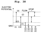
- an electric potential difference A is an electric potential difference
- both the first electric potential V 1 and the fourth electric potential V 4 are the ground electric potential (GND), and further, the second electric potential V 2 is an intermediate electric potential between the first electric potential V 1 and the third electric potential V 3 .
- the electric potential difference between the ink I in contact with the common electrode 17 , and the individual electrode 22 becomes 15 V in the two individual channels 15 positioned at the left end and the center, of the ink channels 12 at the left end and the center.
- this electric potential difference of 15 V is less than the critical electric potential difference Va
- the wetting angle ⁇ of the ink I on the surface of the insulating layer 25 is somewhat decreased but does not become smaller than (or equal to) the critical wetting angle ⁇ a, and the ink I cannot cross over the surface of the insulating layer 25 , and move to the discharge port 15 a .
- the electric potential of the common electrode 17 of the common channel 14 at the center is the ground electric potential
- the electric potential of the common electrode 17 of the left and right common channel 14 is 15 V
- the electric potential of the individual electrode 22 formed on the individual channel 15 positioned at the right end, from among the three individual channels 15 of each ink channel 12 is 30 V.
- the electric potential difference between the ink and the individual electrode 22 becomes greater than the critical electric potential difference Va, and the ink is discharged from the ink port 15 a .
- the individual channels 15 other than this individual channel 15 since the electric potential difference between the ink and the individual electrode 22 is less than the critical electric potential difference, the ink is not discharged.
- the head pressure of the ink tank 2 is applied all the time to the ink in the ink channel 12 to generate the flow of the ink toward the discharge port 15 a . Therefore the ink is discharged assuredly from the discharge port 15 a , when the electric potential difference between the ink and the individual electrode 22 is increased and the wetting angle of the ink on the surface of the insulating layer 25 becomes smaller than or equal to the critical wetting angle ⁇ a.
- the combinations of the four electric potentials V 1 , to V 4 are not restricted to the combinations shown in FIG. 6 of the first embodiment, and can take various values provided that the relations mentioned above (
- all the four electric potentials V 1 to V 4 may be positive electric potentials higher than the ground electric potential, and among these four electric potentials V 1 to V 4 , the third electric potential V 3 may be maximum and the first electric potential V 1 may be minimum.
- the electric potential difference A between the common electrode 17 and the individual electrode 22 , in the individual channel 15 which transports the ink to the discharge port 15 a is increased. Therefore, it is possible to change substantially the electric potential difference A against the electric potential difference B, C and D between the common electrode 17 and the individual electrode 22 in the individual channel 15 which does not transport the ink, and to perform stably the ink transporting operation and the stopping operation.
- the first electric potential V 1 , and the fourth electric potential V 4 were the same electric potentials (refer to FIG. 6 ), but as shown in FIG. 17 and FIG. 18 , the second electric potential V 2 and the third electric potential V 3 , or the second electric potential V 2 and the fourth electric potential V 4 may be the same electric potentials.
- the number of types of the electric potentials applied to the common electrode 17 and the individual electrode 22 from the driver IC 21 is reduced to three, it is possible to make simple the formation of the driver IC 21 , and to reduce the cost thereof.
- FIG. 23 to FIG. 29 a second embodiment of the present invention will be described by referring to FIG. 23 to FIG. 29 .
- the formation of the ink transporting head differs from the formation in the first embodiment, mainly the ink transporting head is described, and the description of formation other than the formation of the ink transporting head, which is almost same as the formation in the first embodiment is omitted.
- the three first channel portions 55 of each ink channel 52 are separated mutually by partition walls 56 extended forward and backward between the three first channel 55 a . Moreover, the first channel 55 a and the second channel 55 b communicate via a leading port 44 a formed on a front surface the box-shaped member 44 .
- the ink transporting head 41 of the second embodiment similarly as in the first embodiment, from the driver IC 61 , when the first electric potential V 1 is applied to the common electrode 57 which is in contact with the ink, and the third electric potential V 3 is applied to the leading electrode 62 or the transporting electrode 66 , since the electric potential difference V 3 ⁇ V 1 becomes greater than or equal to the critical electric potential difference Va (refer to FIG. 5 ), the wetting angle of the ink on the surface of the insulating layer 65 covering the leading electrode 62 or the transporting electrode 66 becomes smaller than or equal to the critical wetting angle ⁇ a. At this time, the ink may exist on the surface of the insulating layer 65 covering the electrode to which the third electric potential V 3 is applied.
- the electric potential (second electric potential) of 15 V is applied from the driver IC 61 to each of the two common electrodes 57 formed on the two common channels 54 , one at the right end and the other at the center.
- the electric potential (third electric potential) of 30 V is applied from the driver IC 61 to the two leading electrodes 62 formed on the two individual channels 55 of each ink channel 52 , one positioned at the right end and the other positioned at the center.
- the matrix drive is available even in the ink transporting head of the second embodiment.
- FIG. 30 to FIG. 35 a third embodiment of the present invention will be described by referring to FIG. 30 to FIG. 35 .
- the formation of the ink transporting head differs from the formation in the first embodiment, mainly the ink transporting head is described, and the description of formation other than the formation of the ink transporting head, which is almost same as the formation in the first embodiment is omitted.
- each common channel 84 On a bottom surface (upper surface of the substrate 73 : channel forming surface) of each common channel 84 , a common electrode 87 which is rectangular shaped in a plan view, and extended over almost entire area in a direction of width of the common channel 84 is formed, and the electroconductive ink in the common channel 84 is in contact all the time with the common electrode 87 .
- the common electrodes 87 provided to the three common channels 84 respectively are connected to a driver IC 91 via an electroconductive material filled in three through holes 88 a , 88 b , and 88 c formed in the substrate 73 , and three wirings 90 a , 90 b , and 90 c formed on a lower surface of the substrate 73 .
- any one of two predetermined electric potentials (the first electric potential V 1 and the second electric potential V 2 ) is selectively applied to each desired common electrode 87 , from the driver IC 91 .
- each individual electrode 92 an insulating layer 95 which covers completely the individual electrodes 92 is formed.
- the wetting angle of the ink on the surface of the insulating layer 95 becomes greater than the wetting angle of the ink on an inner surface of the individual channel 85 in an area in which the insulating layer 95 is not formed, and the ink may not exist on the surface of the insulating layer 95 .
- the electric potential difference B is the electric potential difference
- the electric potential difference C is the electric potential difference
- the electric potential difference D is the electric potential difference
- both the first electric potential V 1 and the third electric potential V 3 are the ground electric potential (GND), and further, the second electric potential V 2 is an intermediate electric potential between the first electric potential V 1 and the fourth electric potential V 4 .
- the difference between the electric potential difference A and the electric potential difference B, C or D is a potential difference between the common electrode 87 and the individual electrode 92 in the individual channel 85 which transports the ink to the discharge port 85 a
- the electric potential difference B, C and D is potential differences between the common electrode 87 and the individual electrode 92 in the individual channel 85 which does not transport the ink.
- both the first electric potential V 1 and the third electric potential V 3 are the ground electric potential
- the types of the electric potentials applied to the common electrode 87 and the individual electrode 92 by the driver IC 91 are reduced to two types namely the second electric potential V 2 and the fourth electric potential V 4 . Therefore, it is possible to make simple the formation of the driver IC 91 , and to reduce the cost of the electric system including the driver IC 91 .
- the ink transporting operation (discharge operation) by the ink transporting head 71 will be described below by referring to FIG. 34 to FIG. 37 .
- the fourth electric potential V 4 is 30 V
- the critical electric potential difference Va is 10 V.
- the ink I is discharged through the discharge port 85 a in the two individual channels 85 of the ink channel 82 on the right end where both the common electrode 87 and the individual electrode 92 are at the ground electric potential.
- the matrix drive is available.
- the combinations of the four electric potentials V 1 to V 4 are not restricted to the combinations shown in FIG. 33 , and can take various values provided the relations mentioned above (
- Some preferable examples of the combinations of these four electric potentials V 1 to V 4 will be described below.
- any one of the four electric potentials V 1 to V 4 is the ground electric potential.
- the first electric potential V 1 is the ground electric potential. In this case, it is possible to make simple the formation of the driver IC 91 , and to reduce the cost, because the types of electric potentials applied to the common electrode 87 and the individual electrode 92 from the driver IC 91 are reduced to three types.
- the first electric potential V 1 and the third electric potential V 3 are the same electric potential. Even in this case, since the types of electric potentials applied to the common electrode 87 and the individual electrode 92 from the driver IC 91 are reduced to three types, it is possible to make simple the formation of the driver IC 91 , and to reduce the cost of the electrical system.
- the second electric potential V 2 is the ground electric potential
Landscapes
- Ink Jet (AREA)
- Particle Formation And Scattering Control In Inkjet Printers (AREA)
- Automatic Analysis And Handling Materials Therefor (AREA)
Applications Claiming Priority (2)
| Application Number | Priority Date | Filing Date | Title |
|---|---|---|---|
| JP2005-249486 | 2005-08-30 | ||
| JP2005249486 | 2005-08-30 |
Publications (2)
| Publication Number | Publication Date |
|---|---|
| US20070070129A1 US20070070129A1 (en) | 2007-03-29 |
| US7686426B2 true US7686426B2 (en) | 2010-03-30 |
Family
ID=37507318
Family Applications (1)
| Application Number | Title | Priority Date | Filing Date |
|---|---|---|---|
| US11/468,483 Expired - Fee Related US7686426B2 (en) | 2005-08-30 | 2006-08-30 | Liquid transporting apparatus and liquid transporting head |
Country Status (4)
| Country | Link |
|---|---|
| US (1) | US7686426B2 (de) |
| EP (1) | EP1759851B1 (de) |
| AT (1) | ATE430032T1 (de) |
| DE (1) | DE602006006510D1 (de) |
Cited By (1)
| Publication number | Priority date | Publication date | Assignee | Title |
|---|---|---|---|---|
| US20080237047A1 (en) * | 2007-03-27 | 2008-10-02 | Brother Kogyo Kabushiki Kaisha | Liquid Transporting Apparatus |
Families Citing this family (2)
| Publication number | Priority date | Publication date | Assignee | Title |
|---|---|---|---|---|
| JP4774977B2 (ja) * | 2005-12-19 | 2011-09-21 | ブラザー工業株式会社 | 液体移送装置 |
| WO2013025543A1 (en) * | 2011-08-12 | 2013-02-21 | Solidus Biosciences, Inc. | Cell chips |
Citations (9)
| Publication number | Priority date | Publication date | Assignee | Title |
|---|---|---|---|---|
| US4855768A (en) * | 1987-03-31 | 1989-08-08 | Minolta Camera Kabushiki Kaisha | Digital printing apparatus |
| JPH02286346A (ja) | 1989-04-28 | 1990-11-26 | Fuji Xerox Co Ltd | カラーインクジェット記録装置 |
| JPH03234628A (ja) | 1990-02-13 | 1991-10-18 | Canon Inc | 液体噴射記録ヘッドおよび該ヘッドを具備する液体噴射記録装置 |
| US5144340A (en) * | 1989-03-10 | 1992-09-01 | Minolta Camera Kabushiki Kaisha | Inkjet printer with an electric curtain force |
| WO1999017083A1 (en) | 1997-09-29 | 1999-04-08 | Sarnoff Corporation | Print array and method of fluid transfer |
| WO2002007503A1 (en) | 2000-07-25 | 2002-01-31 | The Regents Of The University Of California | Electrowetting-driven micropumping |
| JP2003326712A (ja) | 2002-05-16 | 2003-11-19 | Brother Ind Ltd | インクジェットヘッド |
| EP1477230A1 (de) | 2002-02-21 | 2004-11-17 | National Institute of Advanced Industrial Science and Technology | Flüssigkeitsstrahlvorrichtung mit ultrakleinem durchmesser |
| US6926382B2 (en) | 2002-04-25 | 2005-08-09 | Brother Kogyo Kabushiki Kaisha | Ink-jet head and ink-jet printer |
Family Cites Families (3)
| Publication number | Priority date | Publication date | Assignee | Title |
|---|---|---|---|---|
| US6545815B2 (en) | 2001-09-13 | 2003-04-08 | Lucent Technologies Inc. | Tunable liquid microlens with lubrication assisted electrowetting |
| JP2005249486A (ja) | 2004-03-02 | 2005-09-15 | Amusu Kk | 超音波厚み測定方法および装置 |
| JP4595369B2 (ja) | 2004-03-31 | 2010-12-08 | ブラザー工業株式会社 | 液体移送ヘッド及びこれを備えた液体移送装置 |
-
2006
- 2006-08-29 DE DE602006006510T patent/DE602006006510D1/de active Active
- 2006-08-29 EP EP06017997A patent/EP1759851B1/de not_active Not-in-force
- 2006-08-29 AT AT06017997T patent/ATE430032T1/de not_active IP Right Cessation
- 2006-08-30 US US11/468,483 patent/US7686426B2/en not_active Expired - Fee Related
Patent Citations (11)
| Publication number | Priority date | Publication date | Assignee | Title |
|---|---|---|---|---|
| US4855768A (en) * | 1987-03-31 | 1989-08-08 | Minolta Camera Kabushiki Kaisha | Digital printing apparatus |
| US5144340A (en) * | 1989-03-10 | 1992-09-01 | Minolta Camera Kabushiki Kaisha | Inkjet printer with an electric curtain force |
| JPH02286346A (ja) | 1989-04-28 | 1990-11-26 | Fuji Xerox Co Ltd | カラーインクジェット記録装置 |
| JPH03234628A (ja) | 1990-02-13 | 1991-10-18 | Canon Inc | 液体噴射記録ヘッドおよび該ヘッドを具備する液体噴射記録装置 |
| WO1999017083A1 (en) | 1997-09-29 | 1999-04-08 | Sarnoff Corporation | Print array and method of fluid transfer |
| US6231177B1 (en) | 1997-09-29 | 2001-05-15 | Sarnoff Corporation | Final print medium having target regions corresponding to the nozzle of print array |
| WO2002007503A1 (en) | 2000-07-25 | 2002-01-31 | The Regents Of The University Of California | Electrowetting-driven micropumping |
| US20030205632A1 (en) | 2000-07-25 | 2003-11-06 | Chang-Jin Kim | Electrowetting-driven micropumping |
| EP1477230A1 (de) | 2002-02-21 | 2004-11-17 | National Institute of Advanced Industrial Science and Technology | Flüssigkeitsstrahlvorrichtung mit ultrakleinem durchmesser |
| US6926382B2 (en) | 2002-04-25 | 2005-08-09 | Brother Kogyo Kabushiki Kaisha | Ink-jet head and ink-jet printer |
| JP2003326712A (ja) | 2002-05-16 | 2003-11-19 | Brother Ind Ltd | インクジェットヘッド |
Non-Patent Citations (2)
| Title |
|---|
| American Vacuum Society, J. Vac Sci. Technol. A 8 (4), Jul./Aug. 1990 "An Investigation of Electrowetting-based microactuation." |
| European Patent Office, European Search Report for Related EP Application No. 06017997 dated Dec. 20, 2007. |
Cited By (2)
| Publication number | Priority date | Publication date | Assignee | Title |
|---|---|---|---|---|
| US20080237047A1 (en) * | 2007-03-27 | 2008-10-02 | Brother Kogyo Kabushiki Kaisha | Liquid Transporting Apparatus |
| US8075100B2 (en) * | 2007-03-27 | 2011-12-13 | Brother Kogyo Kabushiki Kaisha | Liquid transporting apparatus |
Also Published As
| Publication number | Publication date |
|---|---|
| EP1759851A2 (de) | 2007-03-07 |
| US20070070129A1 (en) | 2007-03-29 |
| EP1759851B1 (de) | 2009-04-29 |
| ATE430032T1 (de) | 2009-05-15 |
| EP1759851A3 (de) | 2008-01-23 |
| DE602006006510D1 (de) | 2009-06-10 |
Similar Documents
| Publication | Publication Date | Title |
|---|---|---|
| US20110242237A1 (en) | Liquid ejecting head, liquid ejecting unit, and liquid ejecting apparatus | |
| US8091994B2 (en) | Liquid droplet jetting apparatus including liquid tank and two heads connected in series | |
| US7527358B2 (en) | Liquid transfer device and liquid transfer head | |
| US20160059546A1 (en) | Liquid ejecting head and liquid ejecting apparatus | |
| US7686426B2 (en) | Liquid transporting apparatus and liquid transporting head | |
| EP1798038B1 (de) | Flüssigkeitstransportvorrichtung | |
| US8708460B2 (en) | Piezoelectric actuator device and printer | |
| US7413287B2 (en) | Liquid discharging apparatus | |
| US8201929B2 (en) | Liquid jetting apparatus | |
| US7780268B2 (en) | Liquid transport apparatus | |
| US7976128B2 (en) | Liquid transporting apparatus and printer | |
| US10994538B2 (en) | Liquid ejecting head and liquid ejecting apparatus | |
| US8075100B2 (en) | Liquid transporting apparatus | |
| US8596763B2 (en) | Liquid droplet transport apparatus | |
| US10889115B2 (en) | Liquid discharge head having a wiring substrate with surface wirings connected at both ends via through-wirings | |
| JP4590949B2 (ja) | インクジェットプリンタ | |
| US11104144B2 (en) | Liquid ejecting head and liquid ejecting apparatus | |
| JP2007090869A (ja) | 液体移送装置及び液体移送ヘッド | |
| CN118514431A (zh) | 液体喷出头以及液体喷出装置 |
Legal Events
| Date | Code | Title | Description |
|---|---|---|---|
| AS | Assignment |
Owner name: BROTHER KOGYO KABUSHIKI KAISHA,JAPAN Free format text: ASSIGNMENT OF ASSIGNORS INTEREST;ASSIGNOR:SUGAHARA, HIROTO;REEL/FRAME:018575/0067 Effective date: 20060928 Owner name: BROTHER KOGYO KABUSHIKI KAISHA, JAPAN Free format text: ASSIGNMENT OF ASSIGNORS INTEREST;ASSIGNOR:SUGAHARA, HIROTO;REEL/FRAME:018575/0067 Effective date: 20060928 |
|
| FPAY | Fee payment |
Year of fee payment: 4 |
|
| FEPP | Fee payment procedure |
Free format text: MAINTENANCE FEE REMINDER MAILED (ORIGINAL EVENT CODE: REM.) |
|
| LAPS | Lapse for failure to pay maintenance fees |
Free format text: PATENT EXPIRED FOR FAILURE TO PAY MAINTENANCE FEES (ORIGINAL EVENT CODE: EXP.) |
|
| STCH | Information on status: patent discontinuation |
Free format text: PATENT EXPIRED DUE TO NONPAYMENT OF MAINTENANCE FEES UNDER 37 CFR 1.362 |
|
| FP | Lapsed due to failure to pay maintenance fee |
Effective date: 20180330 |