US7550726B2 - Electronic device and method for fabricating the same - Google Patents
Electronic device and method for fabricating the same Download PDFInfo
- Publication number
- US7550726B2 US7550726B2 US11/872,934 US87293407A US7550726B2 US 7550726 B2 US7550726 B2 US 7550726B2 US 87293407 A US87293407 A US 87293407A US 7550726 B2 US7550726 B2 US 7550726B2
- Authority
- US
- United States
- Prior art keywords
- heat sensing
- sensing section
- contact
- electronic device
- section
- Prior art date
- Legal status (The legal status is an assumption and is not a legal conclusion. Google has not performed a legal analysis and makes no representation as to the accuracy of the status listed.)
- Expired - Fee Related
Links
- 238000000034 method Methods 0.000 title claims description 41
- 230000000704 physical effect Effects 0.000 claims abstract description 15
- 230000008859 change Effects 0.000 claims abstract description 14
- 239000000758 substrate Substances 0.000 claims description 173
- 230000006698 induction Effects 0.000 claims description 58
- 238000003860 storage Methods 0.000 claims description 43
- 239000000463 material Substances 0.000 claims description 27
- 230000000694 effects Effects 0.000 claims description 6
- 230000005676 thermoelectric effect Effects 0.000 claims description 4
- 230000001678 irradiating effect Effects 0.000 claims description 2
- 239000011253 protective coating Substances 0.000 description 40
- VYPSYNLAJGMNEJ-UHFFFAOYSA-N Silicium dioxide Chemical compound O=[Si]=O VYPSYNLAJGMNEJ-UHFFFAOYSA-N 0.000 description 36
- XUIMIQQOPSSXEZ-UHFFFAOYSA-N Silicon Chemical compound [Si] XUIMIQQOPSSXEZ-UHFFFAOYSA-N 0.000 description 28
- 229910052710 silicon Inorganic materials 0.000 description 28
- 239000010703 silicon Substances 0.000 description 28
- 239000000377 silicon dioxide Substances 0.000 description 18
- 235000012239 silicon dioxide Nutrition 0.000 description 17
- 229910021420 polycrystalline silicon Inorganic materials 0.000 description 16
- 229920005591 polysilicon Polymers 0.000 description 16
- 239000010410 layer Substances 0.000 description 15
- 230000035945 sensitivity Effects 0.000 description 15
- 150000002500 ions Chemical class 0.000 description 14
- 238000004519 manufacturing process Methods 0.000 description 14
- 239000002019 doping agent Substances 0.000 description 11
- 238000009413 insulation Methods 0.000 description 10
- 230000008569 process Effects 0.000 description 9
- 230000005291 magnetic effect Effects 0.000 description 7
- 239000004065 semiconductor Substances 0.000 description 7
- 230000000052 comparative effect Effects 0.000 description 6
- 239000002784 hot electron Substances 0.000 description 6
- 230000002093 peripheral effect Effects 0.000 description 6
- 229910052782 aluminium Inorganic materials 0.000 description 5
- XAGFODPZIPBFFR-UHFFFAOYSA-N aluminium Chemical compound [Al] XAGFODPZIPBFFR-UHFFFAOYSA-N 0.000 description 5
- 239000003990 capacitor Substances 0.000 description 5
- 230000010354 integration Effects 0.000 description 5
- 230000004044 response Effects 0.000 description 5
- 230000001133 acceleration Effects 0.000 description 3
- 230000003247 decreasing effect Effects 0.000 description 3
- 238000005530 etching Methods 0.000 description 3
- 230000005855 radiation Effects 0.000 description 3
- ZOXJGFHDIHLPTG-UHFFFAOYSA-N Boron Chemical compound [B] ZOXJGFHDIHLPTG-UHFFFAOYSA-N 0.000 description 2
- 229910052785 arsenic Inorganic materials 0.000 description 2
- RQNWIZPPADIBDY-UHFFFAOYSA-N arsenic atom Chemical compound [As] RQNWIZPPADIBDY-UHFFFAOYSA-N 0.000 description 2
- 229910052796 boron Inorganic materials 0.000 description 2
- 230000001276 controlling effect Effects 0.000 description 2
- 238000001816 cooling Methods 0.000 description 2
- 230000007423 decrease Effects 0.000 description 2
- 238000006073 displacement reaction Methods 0.000 description 2
- 108010067216 glycyl-glycyl-glycine Proteins 0.000 description 2
- 239000011159 matrix material Substances 0.000 description 2
- 230000007246 mechanism Effects 0.000 description 2
- 229910052751 metal Inorganic materials 0.000 description 2
- 239000002184 metal Substances 0.000 description 2
- 230000002265 prevention Effects 0.000 description 2
- 239000010936 titanium Substances 0.000 description 2
- 229910052613 tourmaline Inorganic materials 0.000 description 2
- 229940070527 tourmaline Drugs 0.000 description 2
- 239000011032 tourmaline Substances 0.000 description 2
- GZXOHHPYODFEGO-UHFFFAOYSA-N triglycine sulfate Chemical compound NCC(O)=O.NCC(O)=O.NCC(O)=O.OS(O)(=O)=O GZXOHHPYODFEGO-UHFFFAOYSA-N 0.000 description 2
- WSMQKESQZFQMFW-UHFFFAOYSA-N 5-methyl-pyrazole-3-carboxylic acid Chemical compound CC1=CC(C(O)=O)=NN1 WSMQKESQZFQMFW-UHFFFAOYSA-N 0.000 description 1
- 229910000838 Al alloy Inorganic materials 0.000 description 1
- -1 As (arsenic) ions Chemical class 0.000 description 1
- 229910015808 BaTe Inorganic materials 0.000 description 1
- 229910002665 PbTe Inorganic materials 0.000 description 1
- RTAQQCXQSZGOHL-UHFFFAOYSA-N Titanium Chemical compound [Ti] RTAQQCXQSZGOHL-UHFFFAOYSA-N 0.000 description 1
- XHCLAFWTIXFWPH-UHFFFAOYSA-N [O-2].[O-2].[O-2].[O-2].[O-2].[V+5].[V+5] Chemical compound [O-2].[O-2].[O-2].[O-2].[O-2].[V+5].[V+5] XHCLAFWTIXFWPH-UHFFFAOYSA-N 0.000 description 1
- 238000010521 absorption reaction Methods 0.000 description 1
- 239000011248 coating agent Substances 0.000 description 1
- 238000000576 coating method Methods 0.000 description 1
- 229910052681 coesite Inorganic materials 0.000 description 1
- 150000001875 compounds Chemical class 0.000 description 1
- 238000007796 conventional method Methods 0.000 description 1
- 229910052906 cristobalite Inorganic materials 0.000 description 1
- 239000013078 crystal Substances 0.000 description 1
- 229910052607 cyclosilicate Inorganic materials 0.000 description 1
- 238000000151 deposition Methods 0.000 description 1
- 238000001514 detection method Methods 0.000 description 1
- NKZSPGSOXYXWQA-UHFFFAOYSA-N dioxido(oxo)titanium;lead(2+) Chemical compound [Pb+2].[O-][Ti]([O-])=O NKZSPGSOXYXWQA-UHFFFAOYSA-N 0.000 description 1
- 238000009826 distribution Methods 0.000 description 1
- 238000001312 dry etching Methods 0.000 description 1
- 239000012777 electrically insulating material Substances 0.000 description 1
- 239000003302 ferromagnetic material Substances 0.000 description 1
- 230000005484 gravity Effects 0.000 description 1
- 229910010272 inorganic material Inorganic materials 0.000 description 1
- 239000011147 inorganic material Substances 0.000 description 1
- 229910052500 inorganic mineral Inorganic materials 0.000 description 1
- 238000005259 measurement Methods 0.000 description 1
- 239000011707 mineral Substances 0.000 description 1
- 238000012986 modification Methods 0.000 description 1
- 230000004048 modification Effects 0.000 description 1
- 239000011368 organic material Substances 0.000 description 1
- 238000000059 patterning Methods 0.000 description 1
- 230000010287 polarization Effects 0.000 description 1
- 238000005498 polishing Methods 0.000 description 1
- 238000012545 processing Methods 0.000 description 1
- 230000001105 regulatory effect Effects 0.000 description 1
- 230000000630 rising effect Effects 0.000 description 1
- 239000002356 single layer Substances 0.000 description 1
- 229910052682 stishovite Inorganic materials 0.000 description 1
- 239000000126 substance Substances 0.000 description 1
- OCGWQDWYSQAFTO-UHFFFAOYSA-N tellanylidenelead Chemical compound [Pb]=[Te] OCGWQDWYSQAFTO-UHFFFAOYSA-N 0.000 description 1
- 229910052719 titanium Inorganic materials 0.000 description 1
- OGIDPMRJRNCKJF-UHFFFAOYSA-N titanium oxide Inorganic materials [Ti]=O OGIDPMRJRNCKJF-UHFFFAOYSA-N 0.000 description 1
- 238000012546 transfer Methods 0.000 description 1
- 230000007704 transition Effects 0.000 description 1
- 229910052905 tridymite Inorganic materials 0.000 description 1
- 229910001935 vanadium oxide Inorganic materials 0.000 description 1
- 238000001039 wet etching Methods 0.000 description 1
- 238000004804 winding Methods 0.000 description 1
- 229910052726 zirconium Inorganic materials 0.000 description 1
Images


Classifications
-
- G—PHYSICS
- G01—MEASURING; TESTING
- G01J—MEASUREMENT OF INTENSITY, VELOCITY, SPECTRAL CONTENT, POLARISATION, PHASE OR PULSE CHARACTERISTICS OF INFRARED, VISIBLE OR ULTRAVIOLET LIGHT; COLORIMETRY; RADIATION PYROMETRY
- G01J5/00—Radiation pyrometry, e.g. infrared or optical thermometry
- G01J5/10—Radiation pyrometry, e.g. infrared or optical thermometry using electric radiation detectors
-
- G—PHYSICS
- G01—MEASURING; TESTING
- G01J—MEASUREMENT OF INTENSITY, VELOCITY, SPECTRAL CONTENT, POLARISATION, PHASE OR PULSE CHARACTERISTICS OF INFRARED, VISIBLE OR ULTRAVIOLET LIGHT; COLORIMETRY; RADIATION PYROMETRY
- G01J5/00—Radiation pyrometry, e.g. infrared or optical thermometry
- G01J5/02—Constructional details
- G01J5/0225—Shape of the cavity itself or of elements contained in or suspended over the cavity
- G01J5/024—Special manufacturing steps or sacrificial layers or layer structures
-
- G—PHYSICS
- G01—MEASURING; TESTING
- G01J—MEASUREMENT OF INTENSITY, VELOCITY, SPECTRAL CONTENT, POLARISATION, PHASE OR PULSE CHARACTERISTICS OF INFRARED, VISIBLE OR ULTRAVIOLET LIGHT; COLORIMETRY; RADIATION PYROMETRY
- G01J5/00—Radiation pyrometry, e.g. infrared or optical thermometry
- G01J5/02—Constructional details
- G01J5/0225—Shape of the cavity itself or of elements contained in or suspended over the cavity
- G01J5/0245—Shape of the cavity itself or of elements contained in or suspended over the cavity for performing thermal shunt
-
- G—PHYSICS
- G01—MEASURING; TESTING
- G01J—MEASUREMENT OF INTENSITY, VELOCITY, SPECTRAL CONTENT, POLARISATION, PHASE OR PULSE CHARACTERISTICS OF INFRARED, VISIBLE OR ULTRAVIOLET LIGHT; COLORIMETRY; RADIATION PYROMETRY
- G01J5/00—Radiation pyrometry, e.g. infrared or optical thermometry
- G01J5/10—Radiation pyrometry, e.g. infrared or optical thermometry using electric radiation detectors
- G01J5/20—Radiation pyrometry, e.g. infrared or optical thermometry using electric radiation detectors using resistors, thermistors or semiconductors sensitive to radiation, e.g. photoconductive devices
-
- G—PHYSICS
- G01—MEASURING; TESTING
- G01J—MEASUREMENT OF INTENSITY, VELOCITY, SPECTRAL CONTENT, POLARISATION, PHASE OR PULSE CHARACTERISTICS OF INFRARED, VISIBLE OR ULTRAVIOLET LIGHT; COLORIMETRY; RADIATION PYROMETRY
- G01J5/00—Radiation pyrometry, e.g. infrared or optical thermometry
- G01J5/10—Radiation pyrometry, e.g. infrared or optical thermometry using electric radiation detectors
- G01J5/34—Radiation pyrometry, e.g. infrared or optical thermometry using electric radiation detectors using capacitors, e.g. pyroelectric capacitors
-
- H—ELECTRICITY
- H01—ELECTRIC ELEMENTS
- H01L—SEMICONDUCTOR DEVICES NOT COVERED BY CLASS H10
- H01L27/00—Devices consisting of a plurality of semiconductor or other solid-state components formed in or on a common substrate
- H01L27/14—Devices consisting of a plurality of semiconductor or other solid-state components formed in or on a common substrate including semiconductor components sensitive to infrared radiation, light, electromagnetic radiation of shorter wavelength or corpuscular radiation and specially adapted either for the conversion of the energy of such radiation into electrical energy or for the control of electrical energy by such radiation
- H01L27/144—Devices controlled by radiation
- H01L27/146—Imager structures
- H01L27/14665—Imagers using a photoconductor layer
- H01L27/14669—Infrared imagers
-
- H—ELECTRICITY
- H01—ELECTRIC ELEMENTS
- H01L—SEMICONDUCTOR DEVICES NOT COVERED BY CLASS H10
- H01L31/00—Semiconductor devices sensitive to infrared radiation, light, electromagnetic radiation of shorter wavelength or corpuscular radiation and specially adapted either for the conversion of the energy of such radiation into electrical energy or for the control of electrical energy by such radiation; Processes or apparatus specially adapted for the manufacture or treatment thereof or of parts thereof; Details thereof
- H01L31/08—Semiconductor devices sensitive to infrared radiation, light, electromagnetic radiation of shorter wavelength or corpuscular radiation and specially adapted either for the conversion of the energy of such radiation into electrical energy or for the control of electrical energy by such radiation; Processes or apparatus specially adapted for the manufacture or treatment thereof or of parts thereof; Details thereof in which radiation controls flow of current through the device, e.g. photoresistors
- H01L31/09—Devices sensitive to infrared, visible or ultraviolet radiation
-
- H—ELECTRICITY
- H01—ELECTRIC ELEMENTS
- H01L—SEMICONDUCTOR DEVICES NOT COVERED BY CLASS H10
- H01L31/00—Semiconductor devices sensitive to infrared radiation, light, electromagnetic radiation of shorter wavelength or corpuscular radiation and specially adapted either for the conversion of the energy of such radiation into electrical energy or for the control of electrical energy by such radiation; Processes or apparatus specially adapted for the manufacture or treatment thereof or of parts thereof; Details thereof
- H01L31/02—Details
- H01L31/02016—Circuit arrangements of general character for the devices
-
- Y—GENERAL TAGGING OF NEW TECHNOLOGICAL DEVELOPMENTS; GENERAL TAGGING OF CROSS-SECTIONAL TECHNOLOGIES SPANNING OVER SEVERAL SECTIONS OF THE IPC; TECHNICAL SUBJECTS COVERED BY FORMER USPC CROSS-REFERENCE ART COLLECTIONS [XRACs] AND DIGESTS
- Y10—TECHNICAL SUBJECTS COVERED BY FORMER USPC
- Y10T—TECHNICAL SUBJECTS COVERED BY FORMER US CLASSIFICATION
- Y10T29/00—Metal working
- Y10T29/49—Method of mechanical manufacture
- Y10T29/49002—Electrical device making
Definitions
- the present invention relates to an electronic device and a method for fabricating an electronic device, and more particularly relates to a thermal infrared sensor and a thermal infrared image sensor.
- An infrared sensor for detecting an electromagnetic wave (or an infrared ray) with a wavelength of 3 ⁇ m to 10 ⁇ m has been used as a heat sensing sensor in crime prevention, measuring, remote sensing and various other fields of applications.
- An infrared image sensor, in which such sensors are arranged as a two-dimensional array, can obtain an even greater amount of information as a thermal image, and has been used extensively in those fields of applications.
- Infrared sensors are roughly classified into quantum sensors and thermal sensors.
- a quantum sensor is a sensor that is made of compound semiconductors and that operates by utilizing the band-to-band transition. Such a quantum sensor has higher sensitivity and higher response speed than a thermal sensor but operates at relatively low temperatures, thus requiring a cooling mechanism. That is why it is difficult to reduce the size or manufacturing cost of such a quantum sensor and it is not easy to apply it to cars, crime prevention tools and various other consumer electronic products.
- thermal sensors have lower sensitivity than a quantum sensor but needs no cooling mechanism. For that reason, it is relatively easy to reduce the size and price of such a sensor, and therefore, it has been used extensively in various consumer electronic products.
- the thermal sensors include thermopile types, bolometer types and pyroelectric types.
- thermopile type includes a portion in which a lot of thermocouples are connected in series together as a thermal sensing portion.
- the thermal sensor may includes a resistor that is made of a material, of which the electrical resistance has significant temperature dependence. By detecting a variation in the amount of current flowing through that resistor, the thermal sensor can measure the temperature. Meanwhile, a pyroelectric type detects charge to be produced on the surface of a tourmaline crystal, for example, as the temperature varies, thereby sensing the temperature variation.
- a thermal sensor of any of these types has a heat insulation structure to prevent the heat from escaping from its infrared sensing portion, thereby maintaining the sensitivity of the sensor reasonably high.
- An exemplary heat insulation structure for such an infrared sensor is disclosed in Japanese Patent Application Laid-Open Publication No. 2003-106896 (hereinafter “Patent Document No. 1”), for example.
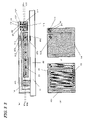
- FIG. 27( b ) is a plan view illustrating main portions of this infrared sensor
- FIG. 27( a ) is a cross-sectional view of the sensor as viewed on the plane 27 b - 27 b.
- the infrared sensor shown in FIG. 27 includes a substrate 240 of silicon, for example, and a photosensitive section 241 that is supported on the substrate 240 .
- the photosensitive section 241 includes a bolometer portion 242 , of which the electrical resistance has temperature dependence, and wiring 243 for measuring the electrical resistance of the bolometer portion 242 .
- the photosensitive section 241 functions as a heat sensing section for the infrared sensor.
- a recess On the upper surface of the substrate 240 that is opposed to the bolometer portion 242 , a recess has been cut so as to leave a gap between the photosensitive section 241 and the substrate 240 .
- a recess may be formed by selectively removing a predetermined region of the substrate 240 by either a wet etching process or a dry etching process.
- the photosensitive section 241 contacts with the substrate 240 at contact portions 245 . Both ends 244 of the wiring 243 extend over the contact portions 245 and are connected to a read circuit (not shown).
- the photosensitive section 241 absorbs an infrared ray
- the temperature at the bolometer portion 242 rises.
- the resistance of the bolometer portion 242 changes.
- current is supplied to the bolometer portion 242 through the wiring 243 and a variation in voltage, caused by the change of resistance, is detected. And based on the magnitude of this voltage variation, the energy of the infrared ray that has been incident on the photosensitive section 241 can be calculated.
- the photosensitive section 241 preferably has a structure that can prevent the thermal energy, produced upon the exposure to the infrared ray, from escaping to the outside.
- the area of contact between the body of the photosensitive section 241 and the substrate 240 is minimized to increase the heat insulation property.
- the portions including both ends 244 of the wiring 243 are elongated portions extending from the body of the photosensitive section 241 to reduce the conduction of the heat to the substrate 240 .
- an infrared sensor is required to further increase its temperature in response to an incoming infrared ray, and eventually exhibit higher infrared sensitivity, by improving its heat insulation property.
- Patent Document No. 2 Japanese Patent Application Laid-Open Publication No. 2002-148111
- a plurality of pixels that are arranged as a two-dimensional array (will be referred to herein as a “heat sensing section”) and horizontal and vertical scanning circuits and other circuits for performing infrared image sensing by driving these pixels (which will be referred to herein as a “detector circuit section”) are integrated together on the same semiconductor substrate.
- electrical switches for sequentially selecting one of those pixels of the heat sensing section after another are arranged on the semiconductor substrate and the heat sensing section and the detector circuit section are electrically connected or disconnected to/from each other by opening and closing those electrical switches.
- the contact portions 245 are interposed between the photosensitive section 241 and the substrate 240 , and therefore, it is difficult to prevent a lot of heat from escaping from the photosensitive section 241 toward the substrate 240 by way of these contact portions 245 . Nevertheless, if the contact portions 245 had an even smaller size, then the resultant rigidity would be too low to support the photosensitive section 245 and the sensor could be broken more easily.
- the heat sensing section and the detector circuit section are electrically connected or disconnected by turning the electrical switches.
- the heat sensing section and the detector circuit section are always connected together in terms of heat conduction. That is to say, those electrical switches cannot interrupt the transfer of heat between the heat sensing section and the detector circuit section.
- an object of the present invention is to provide an electronic device with improved heat insulation properties.
- An electronic device includes: at least one heat sensing section, which includes a first contact portion and of which a physical property varies responsive to an incoming infrared ray; a detector circuit section, which includes a second contact portion and which senses the variation in the physical property of the heat sensing section; and a driving section, which is able to change a first state, in which the first and second contact portions are in contact with each other and electrically connected to each other, into a second state, in which the first and second contact portions are out of contact with each other and electrically disconnected from each other, and vice versa.
- the electronic device includes: a cavity wall portion that defines a cavity housing the heat sensing section inside; and a substrate portion for supporting the cavity wall portion thereon.
- the driving section changes the positions of the heat sensing section inside the cavity.
- the electronic device includes a substrate portion including at least a part of the detector circuit section.
- the detector circuit section includes a contact supporting member that is fixed on the substrate portion.
- the second contact portion is arranged on the surface of the contact supporting member. In the first state, the second contact portion on the contact supporting member is in contact with the first contact portion of the heat sensing section. In the second state, the second contact portion on the contact supporting member is out of contact with the first contact portion of the heat sensing section.
- the second contact portion is arranged on an inner wall of the cavity wall portion. In the first state, the second contact portion on the cavity wall portion is in contact with the first contact portion of the heat sensing section. In the second state, the second contact portion on the cavity wall portion is out of contact with the first contact portion of the heat sensing section.
- the electronic device includes a substrate portion including at least a part of the detector circuit section.
- the second contact portion is arranged on the surface of the substrate portion. In the first state, the second contact portion on the substrate portion is in contact with the first contact portion of the heat sensing section. In the second state, the second contact portion on the substrate portion is out of contact with the first contact portion of the heat sensing section.
- At least a part of the contact supporting member changes its positions between the first and second states.
- At least a part of the heat sensing section changes its positions between the first and second states.
- the driving section moves the heat sensing section to a region where the heat sensing section makes no contact with any other portion of the electronic device.
- the heat sensing section in the second state, is floating in the cavity.
- the electronic device includes a substrate portion.
- the heat sensing section includes a heat sensor supporting portion. In both of the first and second states, the heat sensing section is connected to the substrate portion with the heat sensor supporting portion.
- the heat sensor supporting portion has no wiring portion for electrically connecting the heat sensing section to the detector circuit section.
- the first contact portion includes a plurality of contacts that are arranged on the surface of the heat sensing section.
- the second contact portion includes a plurality of contacts that are arranged on the surface of the substrate portion. In the first state, the contacts on the substrate portion are in contact with the contacts on the heat sensing section. In the second state, the contacts on the substrate portion are out of contact with the contacts on the heat sensing section.
- the electronic device includes a contact supporting member on the substrate portion.
- the second contact portion includes a plurality of contacts that are arranged on the surface of the contact supporting member. In the first state, the contacts of the contact supporting member are in contact with the contacts on the heat sensing section. In the second state, the contacts of the contact supporting member are out of contact with the contacts on the heat sensing section.
- the electronic device includes a cavity wall portion, which is supported on the substrate portion and which defines a cavity housing the heat sensing section inside.
- the second contact portion includes a plurality of contacts that are arranged on an inner wall of the cavity wall portion. In the first state, the contacts on the cavity wall portion are in contact with the contacts on the heat sensing section. In the second state, the contacts on the cavity wall portion are out of contact with the contacts on the heat sensing section.
- the heat sensing section includes an infrared sensing portion, of which the electrical resistance has temperature dependence.
- the detector circuit section when electrically connected to the infrared sensing portion of the heat sensing section, the detector circuit section detects the intensity of the incoming infrared ray based on the electrical resistance of the infrared sensing portion.
- the heat sensing section includes an infrared sensing portion that is made of a material with a thermoelectric effect.
- the heat sensing section includes an infrared sensing portion that is made of a material with a pyroelectric effect.
- the heat sensing section includes an infrared sensing portion, of which the dielectric constant changes with temperatures.
- the driving section includes an electrode or a coil, which is arranged on the substrate portion, the cavity wall portion or the contact supporting member, and is able to exert non-contact force on the heat sensing section.
- the non-contact force is electrostatic force.
- the electronic device includes means for producing electric charge in the heat sensing section by electrostatic induction.
- the heat sensing section includes a charge storage portion to store the electric charge.
- the driving section drives the heat sensing section, which is negatively charged, by repulsive force.
- the heat sensing section includes a ferroelectric material.
- the electrostatic force between the electric charge that has been produced in the substrate, the cavity wall portion or the contact supporting member and polarized charge produced in the ferroelectric material is the non-contact force.
- the non-contact force is electromagnetic force.
- environment surrounding the heat sensing section is shut off from the air and is either a vacuum or a reduced-pressure atmosphere.
- a method for fabricating an electronic device includes the steps of: providing a substrate; forming a heat sensing section, of which a physical property varies responsive to an incoming infrared ray and which is still covered with a sacrificial layer, on the substrate; forming a cavity wall, which surrounds the heat sensing section with the sacrificial layer interposed between them, on the substrate; and etching the sacrificial layer away to separate the heat sensing section from the cavity wall.
- An electronic device driving method is a method for driving an electronic device according to any of the preferred embodiments of the present invention described above.
- the method includes the steps of: (A) irradiating the heat sensing section with an infrared ray; (B) connecting the heat sensing section to the detector circuit section in the first state to detect a variation in a physical property of the heat sensing section; and (C) changing the positions of the heat sensing section to switch its states from the first state into the second state.
- the method includes the step of repeatedly performing the steps (A), (B) and (C) periodically.
- the at least one heat sensing section includes a plurality of heat sensing sections that are arranged in columns and rows, and the steps (A), (B) and (C) are performed at different timings on either a row-by-row basis or a column-by-column basis.
- the heat sensing section is connected in the first state to the detector circuit section for a duration of 1 ⁇ sec to 10 msec.
- the electronic device of the present invention can connect the heat sensing section to the detector circuit section only when necessary by bringing the first contact portion of the heat sensing section and the second contact portion of the detector circuit section into, or out of, contact with each other. If the heat sensing section were always connected to the detector circuit section as in the conventional infrared sensor, it would be impossible to keep the heat from escaping from the heat sensing section. The present invention, however, can minimize such an escape of the heat.
- the heat sensing section can have increased heat insulation, and therefore, the escape of the heat from the heat sensing section to the surrounding environment can be reduced and the temperature of the heat sensing section changes more significantly responsive to an incoming infrared ray. Consequently, the present invention realizes increased infrared responsivity.
- FIG. 1A illustrates a schematic configuration for an electronic device according to the present invention.
- FIG. 1B illustrates an alternative configuration for an electronic device according to the present invention.
- FIG. 2A illustrates a configuration for a heat sensing section according to a first preferred embodiment of the present invention.
- FIG. 2B illustrates an alternative configuration for a heat sensing section according to the first preferred embodiment of the present invention.
- FIG. 3 illustrates a configuration for a charge storage portion according to the first preferred embodiment of the present invention.
- FIG. 4 illustrates a configuration for a cavity wall portion according to the first preferred embodiment of the present invention.
- FIG. 5 illustrates a configuration for a substrate portion according to the first preferred embodiment of the present invention.
- FIG. 6 illustrates an overall configuration for a heat sensing section, a cavity wall portion, and a substrate portion according to the present invention.
- FIG. 7 illustrates an electric circuit configuration according to the present invention.
- FIG. 8A shows how the heat sensing section changes its positions as the electric circuit of the present invention operates.
- FIG. 8B shows how the heat sensing section changes its positions as the electric circuit of the present invention operates.
- FIG. 8C shows how the heat sensing section changes its positions as the electric circuit of the present invention operates.
- FIG. 8D shows how the heat sensing section changes its positions as the electric circuit of the present invention operates.
- FIG. 8E shows how the heat sensing section changes its positions as the electric circuit of the present invention operates.
- FIG. 8F shows how the heat sensing section changes its positions as the electric circuit of the present invention operates.
- FIG. 9 shows how the temperature of the heat sensing section changes with time in the present invention and in a conventional method.
- FIG. 10 shows a method for detecting the position of the heat sensing section of the present invention.
- FIG. 11 illustrates an electric circuit including an upper position detecting electrode portion and an upper position detecting counter electrode portion according to the present invention.
- FIG. 12A is a cross-sectional view illustrating a manufacturing process step to make an electronic device according to the present invention.
- FIG. 12B is a cross-sectional view illustrating another manufacturing process step to make the electronic device of the present invention.
- FIG. 12C is a cross-sectional view illustrating another manufacturing process step to make the electronic device of the present invention.
- FIG. 12D is a cross-sectional view illustrating another manufacturing process step to make the electronic device of the present invention.
- FIG. 12E is a cross-sectional view illustrating another manufacturing process step to make the electronic device of the present invention.
- FIG. 12F is a cross-sectional view illustrating another manufacturing process step to make the electronic device of the present invention.
- FIG. 12G is a cross-sectional view illustrating another manufacturing process step to make the electronic device of the present invention.
- FIG. 12H is a cross-sectional view illustrating another manufacturing process step to make the electronic device of the present invention.
- FIG. 12I is a cross-sectional view illustrating another manufacturing process step to make the electronic device of the present invention.
- FIG. 12J is a cross-sectional view illustrating another manufacturing process step to make the electronic device of the present invention.
- FIG. 12K is a cross-sectional view illustrating another manufacturing process step to make the electronic device of the present invention.
- FIG. 13 illustrates a configuration for a heat sensing section according to a second preferred embodiment of the present invention.
- FIG. 14 illustrates a configuration for a cavity wall portion according to the second preferred embodiment of the present invention.
- FIG. 15 illustrates a configuration for a substrate portion according to the second preferred embodiment of the present invention.
- FIG. 16 illustrates a configuration for a heat sensing section according to a third preferred embodiment of the present invention.
- FIG. 17 illustrates a configuration for a cavity portion according to the third preferred embodiment of the present invention.
- FIG. 18 illustrates a configuration for a substrate portion according to the third preferred embodiment of the present invention.
- FIG. 19 illustrates a schematic configuration for an electronic device according to a fourth preferred embodiment of the present invention.
- FIG. 20 illustrates a configuration for a heat sensing section according to the fourth preferred embodiment of the present invention.
- FIG. 21 illustrates a configuration for a cavity wall portion according to the fourth preferred embodiment of the present invention.
- FIG. 22 illustrates a configuration for a substrate portion according to the fourth preferred embodiment of the present invention.
- FIG. 23 shows a modified operation of the heat sensing section according to the fourth preferred embodiment of the present invention.
- FIG. 24 illustrates a configuration for a heat sensing section according to a fifth preferred embodiment of the present invention.
- FIG. 25 illustrates a configuration for a cavity wall portion according to the fifth preferred embodiment of the present invention.
- FIG. 26 illustrates a configuration for a substrate portion according to the fifth preferred embodiment of the present invention.
- FIG. 27 illustrates a conventional infrared sensor.
- FIG. 28 illustrates a schematic configuration for an electronic device according to a sixth preferred embodiment of the present invention.
- FIG. 29 illustrates a configuration for a heat sensing section according to a sixth preferred embodiment of the present invention.
- FIG. 30 illustrates a configuration for a cavity wall portion according to the sixth preferred embodiment of the present invention.
- FIG. 31 illustrates a configuration for a substrate portion according to the sixth preferred embodiment of the present invention.
- FIG. 32 illustrates a schematic configuration for an electronic device according to a seventh preferred embodiment of the present invention.
- FIG. 33 illustrates a configuration for a heat sensing section and a contact supporting member according to the seventh preferred embodiment of the present invention.
- FIG. 34 illustrates a schematic configuration for an electronic device according to an eighth preferred embodiment of the present invention.
- FIG. 35 illustrates a configuration for a heat sensing section with a multilayer structure.
- FIG. 36 illustrates an exemplary configuration according to another preferred embodiment of the present invention.
- the electronic device of this preferred embodiment is an infrared sensor of a resistance changing type.
- the present invention is in no way limited to this specific preferred embodiment but is also applicable to a pyroelectric infrared sensor, a thermopile type infrared sensor, or any other type of electronic device. The same statement will apply to any of the other preferred embodiments of the present invention to be described later.
- portion (a) is a perspective view illustrating a first preferred embodiment of the present invention and portion (b) is a cross-sectional view thereof as viewed on the plane 1 b - 1 b shown in portion (a) of FIG. 1A .
- the electronic device of this preferred embodiment includes a substrate portion 11 , a cavity wall portion 12 arranged on the upper surface of the substrate portion 11 , and a heat sensing section 13 housed inside the cavity wall portion 12 .
- the substrate portion 11 and/or the cavity wall portion 12 includes an electrode for driving the heat sensing section 13 and a portion (i.e., electric lines) of a detector circuit section.
- a driving section controls the position of the heat sensing section 13 .
- An infrared detector senses a variation in a physical property (such as a variation in electrical resistance) of the heat sensing section 13 .
- the driving section includes an electric or magnetic circuit component such as an electrode or a coil, which is arranged on the substrate portion 11 and/or the cavity wall portion 12 , as one of its elements.
- the “heat sensing section” is defined as a section that absorbs an infrared ray that has been incident on the electronic device of the present invention and changes its temperatures. According to the present invention, the intensity of the incident infrared ray can be detected based on the variation in the temperature of this heat sensing section.
- An exemplary temperature variation of the heat sensing section will be described in detail later.
- a portion of the heat sensing section, of which a physical property changes in response to the variation in the temperature of the heat sensing section upon the exposure to the infrared ray will be referred to herein as an “infrared detecting portion”.
- the heat sensing section 13 of this preferred embodiment can float inside the cavity defined by the cavity wall portion 12 .
- the heat sensing section 13 can be floated by using electrostatic force, for example. While out of contact with the cavity wall portion 12 and the substrate portion 11 , the heat sensing section 13 has a very high heat insulation property. To further improve this heat insulation property, the space inside the cavity may have either a reduced pressure or a vacuum.
- the heat sensing section 13 is not always floated, but when it is necessary to sense a variation in the physical property of that portion of the heat sensing section 13 functioning as an infrared detecting portion, the heat sensing section 13 is moved to make contact with an electrical contact portion of the cavity wall portion 12 . As a result of this contact, the infrared detector can read data (i.e., can make electrical measurement).
- the infrared detecting portion may be made of a material, of which the electrical resistance has temperature dependence. Such a material, of which the electrical resistance changes with the temperature, may be a semiconductor such as silicon.
- An alternative material for the infrared detecting portion may be a material with a thermoelectric effect. Examples of such materials with the thermoelectric effect include BaTe and PbTe.
- Another material for the infrared detecting portion may be a material with a pyroelectric effect. As such a material with a pyroelectric effect, tourmaline, which is a cyclosilicate mineral including boron, has been known.
- Examples of other materials with the pyroelectric effect include inorganic materials such as lead titanate and lithium tantalate and organic materials such as triglycinesulfate (TGS) and polyvinylidenefloride (PVDF).
- TGS triglycinesulfate
- PVDF polyvinylidenefloride
- Still another material for the infrared detecting portion could be a material, of which the dielectric constant changes with the temperature and which may be BTZ (i.e., Ba(Ti, Zr)O 3 ), for example.
- the heat sensing section 13 is illustrated in a simplified form as if it were a flat plate.
- the heat sensing section 13 actually has a bolometer portion and a contact portion as will be described in detail later.
- the heat sensing section 13 preferably has planar dimensions of at most several mm square, and may have a rectangular shape of 30 ⁇ m square, for example. Also, the heat sensing section 13 has a thickness of at most 1 mm, e.g., about 2 ⁇ m in this preferred embodiment. To change the positions of the heat sensing section 13 at high speeds with non-contact force such as electrostatic force, the weight of the heat sensing section 13 is preferably reduced.
- the distance between the heat sensing section 13 and the substrate portion 11 and the distance between the heat sensing section 13 and the cavity wall portion 12 may be within the range of 0.5 ⁇ m to 5 ⁇ m, e.g., about 2 ⁇ m. If the gap left there has such a dimension, the heat sensing section 13 floating can be sufficiently insulated thermally from its surrounding members. As a result, the infrared sensitivity increases.
- FIG. 1B schematically illustrates respective cross sections of electronic devices, in each of which a number of cavities are defined on the same substrate portion 11 and the heat sensing section 13 shown in FIG. 1A is arranged in each of those cavities.
- a one- or two-dimensional array of cells (which will be simply referred to herein as a “cell array”), each having the basic configuration shown in FIG. 1A , is formed on the same substrate portion 11 .
- Such an array of cells can form an infrared image sensor.
- a peripheral circuit including circuit components such as transistors as its elements.
- This peripheral circuit further includes an infrared detector (i.e., a data reading circuit) and a driver for controlling the drive mode of the heat sensing section 13 .
- the heat sensing section 13 and the peripheral circuit can be electrically connected together by way of a contact portion (not shown in FIG. 1A ) that is arranged on the cavity wall portion 12 .
- the contact portion is connected to the peripheral circuit through electric lines (not shown).
- the peripheral circuit reads data on either a row-by-row basis or a column-by-column basis.
- data is sequentially read from the N th row of cells (where N is a natural number) and then from the (N+1) th row of cells in the same way.
- Portion (b) of FIG. 1B shows an example in which the cavity wall portions 12 of respective cells are not separated from each other.
- portion (c) of FIG. 1B shows an example in which a number of heat sensing sections 13 are arranged inside a big cavity.
- the respective heat sensing sections 13 (corresponding to pixels) need to be separated from each other on a cell-by-cell basis, but the cavity portion 12 does not always have to be split into respective cells.
- FIG. 2A illustrates a planar layout for the bolometer portion 21 of the heat sensing section 13 .
- the bolometer portion 21 is made of a material, of which the resistivity depends heavily on the temperature and which may be polysilicon, titanium or vanadium oxide, for example, and has a winding pattern. Both ends of the bolometer portion 21 are connected to bolometer contact portions 24 to be described later.
- the temperature of the bolometer portion 21 rises responsive to an incoming infrared ray, its electrical resistance varies. This variation is sensed by a read circuit section (i.e., the infrared detector section) (not shown). More specifically, the electric lines of the read circuit are electrically connected to the bolometer portion 21 by way of the bolometer contact portions 24 to detect the variation in the resistance of the bolometer portion 21 electrically. As a result, the intensity of the infrared ray that has been incident on the bolometer portion 21 can be calculated.
- a read circuit section i.e., the infrared detector section
- heat sensing sections 13 are arranged in columns and rows on the same substrate portion 11 and if the variations in the electrical resistance of the respective bolometer portions 21 of those heat sensing sections 13 are detected independently of each other, the in-plane distribution of the intensities of the infrared rays can be detected. As a result, an infrared image can be obtained.
- the heat sensing section 13 includes a bolometer protective coating 22 to protect the bolometer portion 21 .
- the bolometer protective coating 22 may be made of an electrically insulating material such as silicon dioxide.
- the heat sensing section 13 of this preferred embodiment further includes charge storage portions 23 to store electric charge therein. When storing electric charge, each of these charge storage portions 23 is negatively charged and can generate electrostatic force between the substrate portion 11 and the electrode arranged on the inner wall of the cavity wall portion 12 . As will be described in detail later, according to this preferred embodiment, the position of the heat sensing section 13 is controlled using this electrostatic force.
- the position of the heat sensing section 13 can be controlled and the states of the heat sensing section 13 can be alternately changed from a first state in which the heat sensing section 13 is in contact with the read circuit section into a second state in which the heat sensing section 13 is out of contact with the read circuit section, and vice versa.
- the heat sensing section 13 in the second state in which the heat sensing section 13 is out of contact with the read circuit section is preferably moved to a region where the heat sensing section 13 makes no contact with any other member of the electronic device.
- the bolometer contact portions 24 of the heat sensing section 13 function as points of contact with the electric lines of the cavity wall portion 12 when current is supplied to the bolometer portion 21 .
- bolometer line contact portions 42 to make contact with the bolometer contact portions 24 are arranged on the upper part of the cavity wall portion 12 .
- the heat sensing section 13 moves, the bolometer contact portions 24 contact with the bolometer line contact portions 42 on the cavity wall portion 12 , thus supplying current from the cavity wall portion 12 to the bolometer portion 21 .
- portion (a) illustrates a detailed cross section of the heat sensing section 13 as viewed on the plane 1 b - 1 b shown in FIG. 1A and portion (b) illustrates the upper surface of the heat sensing section 13 .
- a plane 2 a - 2 a corresponding to the plane 1 b - 1 b is also shown in portion (b) of FIG. 2B just for reference.
- the bolometer portion 21 is coated with the bolometer protective coating 22 .
- the upper and lower surfaces of the bolometer protective coating 22 have been substantially flattened and the bolometer protective coating 22 has a roughly thin plate shape.
- eight separated upper position detecting electrode portions 261 , a source contact portion 26 , a drain contact portion 27 , a gate contact portion 28 and a channel contact portion 29 are arranged as shown in portion (b) of FIG. 2B .
- These contact portions 26 , 27 , 28 and 19 have something to do with the operation of the charge storage portions 23 as will be described in detail later.
- An electrostatic induction electrode portion 25 is arranged in a region of the bolometer protective coating 22 near the upper surface thereof. As shown in portion (b) of FIG. 2B , the electrostatic induction electrode portion 25 has a band shape surrounding the center region in which the charge storage portions 23 are arranged.
- the electrostatic induction electrode portion 25 may be made of polysilicon that has been heavily doped with dopant ions, for example.
- lower position detecting electrode portions 262 On the lower surface of the bolometer protective coating 22 , arranged are lower position detecting electrode portions 262 as shown in portion (a) of FIG. 2B .
- the structure and arrangement of the lower position detecting electrode portions 262 correspond to those of the upper position detecting electrode portions 261 .
- the heat sensing section 13 is roughly rectangular.
- the bolometer contact portions 24 are provided as elongated branch portions extending from the body of the heat sensing section 13 .
- Such a branch structure is adopted in order to minimize the outflow of the heat from the heat sensing section 13 toward the cavity wall portion 12 when the bolometer contact portions 24 are in contact with the cavity wall portion 12 by decreasing the thermal conductivity. Nonetheless, such a branch structure is not indispensable.
- FIG. 3( a ) is a partially enlarged top view of the charge storage portion 23 .
- FIG. 3( b ) is a further enlarged top view illustrating some of a huge number of charge storage elements 31 included in the charge storage portion 23 .
- FIG. 3( c ) is a cross-sectional view of the charge storage element as viewed on the plane 3 c - 3 c shown in FIG. 3( b ).
- the charge storage portion 23 of this preferred embodiment has a configuration in which a number of charge storage elements 31 are arranged in columns and rows to form a matrix array.
- Each of these charge storage elements 31 has an MOS structure as shown in FIG. 3( b ), and includes a source region 32 , a drain region 34 and a channel region 33 that have been defined in a semiconductor layer of polysilicon, for example.
- the channel region 33 has been doped with dopant ions such as B (boron) ions relatively lightly.
- the source and drain regions 32 and 34 have been doped with dopant ions such as As (arsenic) ions relatively heavily.
- the charge storage portion 23 includes a floating gate electrode 35 that has been formed so as to cover the channel region 33 with a gate insulating film interposed between them and a control gate electrode 36 that has been stacked over the floating gate electrode 35 with an insulating film sandwiched between them.
- the floating gate electrode 35 may be made of polysilicon and may have been heavily doped with dopant ions such as As (arsenic) ions, for example.
- the floating gate electrode 35 is electrically isolated from the other portions and stores electric charge therein in the same way as EPROM's write operation.
- the charge storage portion 23 further includes a drain contact portion 37 and a source contact portion 38 that are connected to the drain region 34 and the source region 23 , respectively, a channel contact portion 310 connected to the channel region 33 , and a gate contact portion 39 connected to the control gate electrode 39 .
- the drain contact portion 37 , the source contact portion 38 , the gate contact portion 39 and the channel contact portion 310 may be made of aluminum (Al), for example, and function as terminals for electrically connecting the drain region 34 , the source region 32 , the control gate electrode 36 and the channel region 33 to external circuits, respectively.
- the source contact portion 38 and the channel contact portion 310 are electrically grounded, while a high voltage of 10 V, for example, is applied to the drain contact portion 37 , the drain contact portion 37 and the gate contact portion 39 (i.e., a write operation is performed). Then, electrons move through the channel region 33 from the source region 32 toward the drain region 34 and get high kinetic energy in the vicinity of the drain region 34 to be hot electrons, some of which penetrate the insulating film under the floating gate electrode 35 and are injected into the floating gate electrode 35 . Those electrons that have been injected into the floating gate electrode 35 in this manner are stored inside the floating gate electrode 35 to charge the floating gate electrode 35 negatively.
- the heat sensing section 13 is moved upward such that the respective contact portions 37 , 38 , 39 and 310 arranged on the upper surface of the heat sensing section 13 contact with their associated contact portions on the cavity wall portion 12 as will be described later.
- FIG. 4( a ) is a detailed cross-sectional view of the cavity wall portion 12 as viewed on the plane 1 b - 1 b shown in FIG. 1A
- FIG. 4( b ) is a cross-sectional view as viewed on the plane 4 b - 4 b shown in FIG. 4( a ).
- FIG. 4 the configurations of the heat sensing section 13 and the substrate portion 11 are simplified.
- the cavity wall portion 12 of this preferred embodiment includes contact portions, which are arranged so as to contact with their associated contact portions of the heat sensing section 13 .
- the cavity wall portion 12 includes bolometer line contact portions 42 , a source line contact portion 43 , a drain line contact portion 44 , a gate line contact portion 45 and a channel line contact portion 46 , which respectively contact with the bolometer contact portions 24 , the source contact portion 26 , the drain contact portion 27 , the gate contact portion 28 and the channel contact portion of the heat sensing section 13 shown in FIG. 2B , thereby connecting the bolometer portion 21 , the source region 32 , the drain region 34 , the control gate electrode 36 and the channel region 33 to electric lines that are arranged inside the cavity wall portion 33 .
- Each of these contact portions 42 to 46 is preferably made of a patterned aluminum film and is connected to its associated electric line that is arranged inside the cavity wall portion 12 . In FIG. 4 , some of those electric lines are not illustrated. But these electric lines are also preferably made of a patterned aluminum film, for example.
- the electric lines of the cavity wall portion 12 have the function of electrically connecting the contact portions 42 to 46 to a read circuit, for example.
- the cavity wall portion 12 includes a cavity wall silicon portion 48 , a cavity wall protective coating 49 , an electrostatic induction counter electrode portion 410 , and upper position detecting counter electrode portions 263 .
- the cavity wall silicon portion 48 supports the respective parts of the cavity wall portion 12 , and may be made of polysilicon, for example, and transmits an infrared ray.
- the cavity wall protective coating 49 may be made of silicon dioxide, for example, and protects the respective parts of the cavity wall portion 12 .
- An upper uplifting electrode portion 41 may be made of polysilicon that has been heavily doped with dopant ions, for example, and is electrically connected to the electric lines described above. When a voltage is applied to the upper uplifting electrode portion 41 , repulsive or attractive electrostatic force is produced with respect to the hot electrons that are stored in the charge storage portions 23 of the heat sensing section 13 . By adjusting this force, the position of the heat sensing section 13 can be controlled.
- the electrostatic induction counter electrode portion 410 may be made of polysilicon that has been heavily doped with dopant ions, for example, and are electrically connected to the electric lines arranged inside the cavity wall portion 12 .
- a negative voltage is applied to the electrostatic induction counter electrode portion 410 , electric charge is produced on the upper surface portion of the electrostatic induction counter electrode portion 410 .
- attractive force is produced between the upper uplifting electrode portion 41 and the electrostatic induction counter electrode portion 410 . By using this attractive force, the heat sensing section 13 can be moved upward.
- FIG. 5( a ) is a detailed cross-sectional view of the substrate portion 11 as viewed on the plane 1 b - 1 b shown in FIG. 1A
- FIG. 5( b ) is a cross-sectional view as viewed on the plane 5 b - 5 b shown in FIG. 5( a ).
- FIG. 5 the configurations of the cavity wall portion 12 and the heat sensing section 13 are simplified.
- the substrate portion 11 includes a silicon substrate portion 51 and the lower uplifting electrode portion 52 and lower position detecting counter electrode portions 264 that are supported on the silicon substrate portion 51 .
- the lower uplifting electrode portion 52 and lower position detecting counter electrode portions 264 have been patterned so as to have the layout shown in FIG. 5( b ) and are coated with a substrate protecting coating 53 made of silicon dioxide, for example.
- the lower uplifting electrode portion 52 may be made of polysilicon that has been heavily doped with dopant ions, for example, and is electrically connected to the electric lines that are arranged either on or inside the substrate portion 11 . These electric lines may be formed by a normal semiconductor device fabricating process and may be made of polysilicon that has been heavily doped with dopant ions, an aluminum alloy or a doped region of a silicon substrate to which dopant ions have been implanted at a high doping level.
- repulsive force is produced between the charge storage portions 23 of the heat sensing section 13 and the lower uplifting electrode portion by applying a negative voltage to the lower uplifting electrode portion 52 .
- the position of the heat sensing section 13 can be controlled.
- FIG. 6 is a cross-sectional view illustrating the overall configuration of the heat sensing section 13 , the cavity wall portion 12 and the substrate portion 11 described above.
- the upper uplifting electrode portion 41 consists of electrodes F 1 through F 4
- the lower uplifting electrode portion 52 consists of electrodes F 5 through F 8
- Variable power supplies V 1 through V 8 are connected to the electrodes F 1 through F 8 , respectively.
- the heat sensing section 13 is located between the upper and lower uplifting electrode portions 41 and 52 .
- variable voltage supply V 9 is connected to the electrostatic induction counter electrode portion 410 . Also, the source line contact portion 43 and the channel line contact portion 46 are grounded. Meanwhile, the drain line contact portion 44 is connected to a variable voltage supply Vd and the gate line contact portion 45 is connected to a variable voltage supply Vg.
- FIGS. 8A through 8F and FIG. 9 how the infrared sensor of this preferred embodiment operates.
- FIGS. 8A through 8F are cross-sectional views illustrating how the heat sensing section 13 changes its positions according to the potentials at the respective electrodes.
- the A-A′ and B-B′ cross sections are respectively viewed on the planes A-A′ and B-B′ shown in FIG. 7 .
- FIG. 9 shows how the temperature of the heat sensing section 13 varies with the intensity of the incoming infrared ray, which may be one of three different values #1, #2 and #3, for the infrared sensor of this preferred embodiment and a comparative example with the conventional structure.
- FIG. 9 also shows how the switches of the electric circuit operate and how the variable voltages change its levels with time.
- the level change of the variable voltage schematically shows a variation in voltage value. As will be described later, the variable voltage has a voltage value that always varies slightly to adjust the position of the heat sensing section 13 . However, that small variation is not shown in FIG. 9 .
- FIG. 8B shows a state in which electric charge is stored in the charge storage portions 23 .
- variable voltage supplies V 1 through V 8 are connected to the upper uplifting electrode portion 41 (consisting of the electrodes F 1 through F 4 ) and the lower uplifting electrode portion 52 (consisting of the electrodes F 5 through F 8 ).
- the negative voltage of the variable voltage supply V 9 that is connected to the electrostatic induction counter electrode portion 410 stops being applied and the voltage V 9 is set equal to zero.
- the position of the heat sensing section 13 can be detected by the method to be described in detail later. If the magnitudes of the voltages applied to the upper and lower uplifting electrode portions 41 and 52 are adjusted, and if the position of the heat sensing section 13 is appropriately controlled, by performing a feedback control based on this detected value, the heat sensing section 13 can be kept raised continuously.
- a large positive voltage is applied to the variable voltage supplies V 1 and V 3
- a negative voltage is applied to the variable voltage supplies V 5 , V 6 , V 7 and V 8
- a small negative voltage is applied to the variable voltage supplies V 2 and V 4 .
- strong attractive force is produced between the electrodes F 1 and F 3 of the upper uplifting electrode portion 41 and the charge storage portions 23 of the heat sensing section 13
- repulsive force is produced between the electrode F 5 , F 6 , F 7 and F 8 of the lower uplifting electrode portion 52 and the charge storage portions 23 of the heat sensing section 13 .
- the heat sensing section 13 moves upward.
- the position of the heat sensing section 13 can be adjusted such that the bolometer contact portions 24 contact with the bolometer line contact portions 42 as shown in FIG. 8D by performing a feedback control based on the detected position.
- the heat sensing section 13 in the state shown in FIG. 8D has shifted horizontally compared to the states shown in FIGS. 8A and 8B .
- the source contact portion 38 , the drain contact portion 37 , the gate contact portion 39 and the channel contact portion 310 do not contact with the source line contact portion 43 , the drain line contact portion 44 , the gate line contact portion 45 and the channel line contact portion 46 , respectively.
- the read circuit and the voltage supply V 0 are connected to the bolometer line contact portions 42 (see FIG. 7 ).
- the read circuit includes an integrator and a switch SW R for resetting the integrator.
- Another switch SW 1 is arranged between the bolometer line contact portions 42 and the integrator. In the initial state, the switch SW 1 is in OFF state and the switch SW R is in ON state. But in the state i 3 shown in FIG. 8D , the switches SW 1 and SW R are turned ON and OFF, respectively, at a time t 5 .
- the switches SW 1 and SW R are turned OFF and ON, respectively. Then, the current stops being supplied to the bolometer portion 21 and the integrator is reset as shown in FIG. 8F .
- the current is also supposed to stop being supplied to the bolometer portion 21 at the time t 6 .
- the amounts of current flowing through the bolometer portion 21 are integrated and the resultant integral is output.
- the value of the read circuit is sampled and held just before the time t 6 and the intensity of the incoming infrared ray is calculated based on that value.
- the temperature of the heat sensing section 13 In the period from the time t 0 through the time t 3 , no infrared ray has been incident yet and the temperature of the heat sensing section 13 is kept equal to that of the external environment. In the interval between the times t 3 and t 4 , however, the temperature of the heat sensing section 13 increases due to the incidence of an infrared ray. In this preferred embodiment, however, the heat sensing section 13 is out of contact with the cavity wall portion 12 and the substrate portion 11 , and therefore, the heat escapes from the heat sensing section 13 as radiated heat and as a gas. That is why the increase in temperature in this preferred embodiment is much greater than in the comparative example and the temperature of the heat sensing section changes significantly with the intensity of the incoming infrared ray.
- the bolometer contact portions 24 contact with the bolometer line contact portions 42 and a greater quantity of heat escapes. As a result, the temperature of the heat sensing section 13 decreases. In the comparative example, on the other hand, the temperature of the heat sensing section 13 keeps rising slowly as in the interval between the times t 3 and t 4 .
- the temperature of the heat sensing section 13 rises steeply due to the Joule heat generated.
- the temperature of the heat sensing section 13 changes differently according to the intensity of the incoming infrared ray, and the amount of current flowing through the bolometer portion 21 is determined by the temperature of the heat sensing section 13 . That is why the integrated value of the amount of current flowing through the bolometer in the interval between the times t 5 and t 6 changes with the intensity of the incoming infrared ray.
- the variation in the integrated value of the amount of current flowing through the bolometer in the interval between the times t 5 and t 6 is used as a signal value representing the intensity of the incoming infrared ray.
- the heat sensing section 13 by raising the heat sensing section 13 before current is supplied to the bolometer portion 21 , the variation in the temperature of the heat sensing section 13 is increased. As a result, the signal value representing the intensity of the incoming infrared ray also increases, and eventually the infrared sensitivity can be increased.
- the bolometer contact portions 24 and the bolometer line contact portions 42 out of contact with each other before current is supplied to the bolometer portion 21 , the quantity of heat escaping from the heat sensing section 13 to the external environment can be reduced. Also, when current starts being supplied to the bolometer portion 21 , the bolometer contact portions 24 and the bolometer line contact portions 42 come into contact with each other, thus reading a signal.
- the temperature of the heat sensing section 13 varies more significantly in response to an incoming infrared ray, and the infrared sensitivity can be increased as a result.
- FIG. 9 shows not only how the temperature of the heat sensing section has varied since the time t 6 but also how the temperature of the heat sensing section would vary from the time t 6 on if current were continuously supplied to the bolometer and integrated together.
- the integration time between the times t 5 and t 6 may be defined as follows.
- the thermal conductance from the heat sensing section 13 toward the external environment during the integration is 5 ⁇ 10 ⁇ 7 W/K and the heat capacity of the heat sensing section 13 is 2.5 ⁇ 10 ⁇ 9 J/K, for example.
- the thermal time constant is 5 msec. That is why even if the integration time were increased to more than 5 msec, the temperature of the heat sensing section 13 would settle at a substantially constant value and the sensitivity could not be increased significantly.
- the integration time is preferably shortened.
- the integration time could be defined to be 5 msec, for example.
- the duration in which the heat sensing section 13 stays in contact with the contact portions of the cavity wall portion 12 and connected to the circuit changes according to the size of the heat sensing section 13 and the type of the infrared detecting section, but may be in the range of 1 ⁇ sec to 10 msec, for example.
- the position of the heat sensing section 13 is detected by the upper and lower position detecting electrode portions 261 and 262 of the heat sensing section 13 , the upper position detecting counter electrode portion 263 of the cavity wall portion 12 and the lower position detecting counter electrode portion 264 of the substrate portion 11 .
- the upper position detecting electrode portion 261 consists of eight electrodes in total, each of which may be made of polysilicon that has been heavily doped with dopant ions. Two adjacent ones of these eight electrodes are connected together with an electric line and have an equal potential level.
- the lower position detecting electrode portion 262 has the same configuration as the upper position detecting electrode portion 261 .
- the upper position detecting counter electrode portion 263 of the cavity wall portion 12 consists of eight electrodes in total, each of which may be made of polysilicon that has been heavily doped with dopant ions.
- the upper position detecting counter electrode portion 263 two adjacent ones of these eight electrodes are connected together with an electric line by way of an RF power supply and a current measuring portion as shown in FIG. 10 .
- the respective electrodes of the upper position detecting counter electrode portion 263 are arranged so as to face their associated electrodes of the upper position detecting electrode portion 261 . And these two groups of electrodes form a single capacitor.
- Capacitors Ca and Cb are formed between two pairs of opposed electrodes of the upper position detecting electrode portion 261 and the upper position detecting counter electrode portion 263 .
- An electrostatic capacitance C 1 formed by connecting these capacitors Ca and Cb in series together can be calculated by measuring the amount of current flowing through this circuit when an RF voltage is applied thereto.
- the capacitors formed between the electrodes of the upper position detecting electrode portion 261 and their associated electrodes of the upper position detecting counter electrode portion 263 define electrostatic capacitances C 2 , C 3 and C 4 as well as the electrostatic capacitance C 1 described above. And the values of these capacitances C 2 , C 3 and C 4 can be measured by the method described above.
- the lower position detecting counter electrode portion 264 has the same configuration as the upper position detecting counter electrode portion 263 and the capacitors formed between the electrodes of the lower position detecting electrode portion 262 and their associated electrodes of the lower position detecting counter electrode portion 264 define electrostatic capacitances C 5 , C 6 , C 7 and C 8 . And the values of these capacitances C 5 , C 6 , C 7 and C 8 can be measured by the method described above (see FIG. 11 ).
- the electrostatic capacitances C 1 through C 8 change with the position of the heat sensing section 13 . That is to say, each of the electrostatic capacitances C 1 through C 8 can be represented as a function of six variables representing the displacement and angle of rotation of the heat sensing section. If these functions are calculated in advance, then the position of the heat sensing section 13 can be sensed by detecting the values of the electrostatic capacitances C 1 through C 8 .
- the displacement of the heat sensing section 13 due to the variation in voltage could be reduced to a negligible level.
- the heat sensing section 13 is designed so as to be out of contact with any other portion when the bolometer contact portions 24 of the heat sensing section 13 are brought into contact with the bolometer line contact portions 42 (see FIG. 8D ). That is to say, the infrared sensor of this preferred embodiment is designed so as to have its overall contact point area minimized.
- parts of the heat sensing section 13 that would come close to the bolometer contact portions 24 are elongated portions extending from the body of the heat sensing section 13 . That is why when current is supplied to the bolometer portion 21 , the escape of the heat can be minimized. As a result, the infrared responsivity can be increased.
- the heat sensing section 13 is raised again.
- the temperature of the heat sensing section 13 can recover its steady state in a shorter time.
- a positive voltage to the variable voltage supply V 2 attractive force can be produced between the electrode F 2 and the charge storage portions 23 and the heat sensing section 13 can be brought into contact with the cavity wall portion 12 at the electrode F 2 .
- that interval can also be shortened by applying negative voltages to the variable voltage supplies V 1 through V 4 and positive voltages to the variable voltage supplies V 5 through V 8 to bring the heat sensing section 13 into contact with the substrate portion 11 in a broad area.
- FIGS. 12A through 12K a preferred embodiment of a method for fabricating an electronic device according to the present invention will be described with reference to FIGS. 12A through 12K .
- the substrate portion 11 shown in FIG. 12A is prepared. Specifically, first, a silicon substrate 901 is provided and a substrate protective coating 903 of silicon dioxide is deposited on the silicon substrate 901 .
- the substrate protective coating 903 may be deposited by a CVD process, for example.
- a lower uplifting electrode portion 52 and lower position detecting counter electrode portions 264 are formed. These electrode portions 52 and 264 can be formed by depositing a polysilicon film and then patterning the polysilicon film by photolithographic and etching processes. The planar layout of the lower uplifting electrode portion 52 and the lower position detecting counter electrode portions 264 is as shown in FIG. 5( b ).
- a silicon dioxide film is deposited over the silicon substrate 901 so as to cover the lower uplifting electrode portion 52 and the lower position detecting counter electrode portions 264 , and then has its surface planarized by a CMP (chemical mechanical polishing) process.
- the planarized silicon dioxide film and the silicon dioxide film that is already present under the electrode portions 52 and 234 together form the substrate protective coating 903 . In this manner, the substrate portion 11 shown in FIG. 12A can be obtained.
- a sacrificial layer 101 of polysilicon is formed over the substrate portion 11 .
- a bolometer protective coating 22 of silicon dioxide is deposited on the sacrificial layer 101 .
- a silicon dioxide film is deposited so as to cover the electrode portions 262 .
- a bolometer portion 21 and charge storage portions 23 are formed.
- the bolometer portion 21 and the charge storage portions 23 may have the planar layout shown in FIG. 2A .
- FIG. 12D these portions are covered with a silicon dioxide film, and an electrostatic induction electrode portion 25 and upper position detecting electrode portions 261 are formed thereon and then covered with a silicon dioxide film.
- the electrostatic induction electrode portion 25 and upper position detecting electrode portions 261 may have the planar layout shown in portion (b) of FIG. 2B .
- a bolometer contact portion 24 , a source contact portion 26 , a drain contact portion 27 , a gate contact portion 28 and a channel contact portion 29 are formed at the respective positions shown in portion (b) of FIG. 2B .
- the silicon dioxide film is patterned to obtain the structure shown in FIG. 12E .
- a method for forming a single heat sensing section 13 has been described with reference to these drawings, a lot of heat sensing sections 13 may be arranged on the same substrate portion 11 and each of the heat sensing sections 13 may be surrounded with the cavity wall portion 12 . In that case, the same structures as that shown in FIG. 12E are formed in the regions that are not shown in FIG. 12E .
- a sacrificial layer of polysilicon is deposited so as to cover all of these portions and then patterned to obtain the structure shown in FIG. 12F .
- a CMP process for planarizing the surface of a film deposited may be performed as needed.
- a cavity wall protective coating 49 of silicon dioxide is deposited first. Thereafter, an electrostatic induction counter electrode portion 410 , an upper uplifting electrode portion 41 , upper position detecting counter electrode portions 263 , bolometer line contact portions 42 , a source line contact portion 43 , a drain line contact portion 44 , a gate line contact portion 45 and a channel line contact portion 46 are formed. These electrode portions and contact portions are designed so as to be aligned with their associated electrode portions and contact portions in the heat sensing section 12 .
- this structure is covered with a silicon dioxide film as shown in FIG. 12H .
- a polysilicon film is deposited on the silicon dioxide film and then patterned, thereby forming a cavity wall silicon portion 48 as shown in FIG. 12I .
- another silicon dioxide film is deposited on the cavity wall silicon portion 48 and then patterned to obtain the structure shown in FIG. 12J .
- a CMP process for planarizing the surface of a film deposited may be performed as needed.
- the sacrificial layer 101 is removed as shown in FIG. 12K .
- the sacrificial layer 101 could be removed by an isotropic etching process using XeFe gas, for example.
- the heat sensing section 13 is separated from the substrate portion 11 and the cavity wall portion 12 .
- the manufacturing process described above may be carried out by techniques and equipment that are normally adopted in semiconductor device processing.
- a method for fabricating an electronic device with only one heat sensing section 13 has been described. However, this method is easily applicable for use to make a line sensor or an image sensor with an array of cells.
- each charge storage element 31 is arranged so as not to overlap with the electrostatic induction electrode portion 25 or the bolometer portion 21 . If the charge storage element 31 overlapped with the electrostatic induction electrode portion 25 or the bolometer portion 21 , the negative charge stored in the charge storage element 31 would cause electrostatic induction and would produce positive charge on either the surface of the electrostatic induction electrode portion 25 or that of the bolometer portion 21 . In that case, most of the electric lines of force emitted from this positive charge would enter the negative charge of the charge storage element 31 .
- the charge storage element 31 is arranged so as not to overlap with the electrostatic induction electrode portion 25 or the bolometer portion 21 as viewed perpendicularly to the substrate.
- the respective electric lines and contact portions are preferably made of a metal. But as these lines and portions are arranged on the periphery of the heat sensing section 13 and the cavity wall portion 12 , the metal does not cut off the infrared ray so much, and the infrared responsivity can be kept high.
- electrodes may be arranged around the upper and lower uplifting electrode portions 41 and 52 and the voltages at these surrounding electrodes may always kept equal to zero such that the influence of the variation in the external voltage is reduced.
- an electrode for detecting the position of the heat sensing section 13 and an electrode for changing the positions of the heat sensing section 13 are provided separately.
- a configuration in which a single electrode performs both of these functions may also be adopted.
- a single electrode is connected to an RF voltage source to detect the position of the heat sensing section 13 and to a DC power supply to change the positions of the heat sensing section 13 .
- the electrostatic force for raising the heat sensing section 13 may have a magnitude of about 1 ⁇ 10 ⁇ 8 N. Supposing the heat sensing section 13 has a mass of 1 ⁇ 10 ⁇ 12 kg, for example, when an acceleration of 100 G, which is 100 times as large as the acceleration of gravity, is produced in the device, inertial force of about 1 ⁇ 10 ⁇ 9 N will be produced in the heat sensing section 13 . Under the inertial force of such magnitude, the heat sensing section 13 can be held with stability.
- the repulsive force of the electrostatic force is used to raise the heat sensing section 13 .
- the shorter the distance the greater this repulsive force. That is why if the heat sensing section 13 has moved from an equilibrium position due to the application of acceleration to the device, for example, then restitution force will be produced to cause the heat sensing section 13 to go back to its position of equilibrium. For that reason, the heat sensing section 13 can be kept raised with stability by a relatively simple control method.
- the position of the heat sensing section 13 is controlled using the electrostatic force of electric charge that has been produced in the heat sensing section 13 as a result of electrostatic induction.
- the overall configuration of the infrared sensor of this preferred embodiment is as shown in FIG. 1 .
- FIG. 13( a ) is a cross-sectional view as viewed on the plane 1 b - 1 b shown in FIG. 1A , illustrating the configuration of the heat sensing section 13 in detail.
- FIG. 13( b ) is a cross-sectional view as viewed on the plane 13 b - 13 b shown in FIG. 13( a )
- FIG. 13( c ) is a cross-sectional view as viewed on the plane 13 c - 13 c shown in FIG. 13( a ).
- the heat sensing section 13 of this preferred embodiment includes a bolometer portion 21 , a bolometer protective coating 22 , a bolometer contact portion 24 , an upper electrostatic induction electrode portion 111 , a lower electrostatic induction electrode portion 112 , an upper position detecting electrode portion 261 and a lower position detecting electrode portion 262 .
- the bolometer portion 21 , the bolometer protective coating 22 and the bolometer contact portion 24 have the same configurations and functions as their counterparts of the first preferred embodiment described above.
- FIG. 14( a ) is a cross-sectional view as viewed on the plane 1 b - 1 b shown in FIG. 1A
- FIG. 14( b ) is a cross-sectional view as viewed on the plane 14 b - 14 b shown in FIG. 14( a ).
- the cavity wall portion 12 includes an upper uplifting electrode portion 41 , bolometer line contact portions 42 , electric lines (not shown), a cavity wall silicon portion 48 , a cavity wall protective coating 49 , an upper electrostatic induction counter electrode portion 121 and an upper position detecting counter electrode portion 263 .
- the bolometer line contact portions 42 , the electric lines, the cavity wall silicon portion 48 , and the cavity wall protective coating 49 are the same as their counterparts of the first preferred embodiment described above.
- FIG. 15( a ) is a cross-sectional view as viewed on the plane 1 b - 1 b shown in FIG. 1A , illustrating the configuration of the substrate portion 11 in detail.
- FIG. 15( b ) is a cross-sectional view as viewed on the plane 15 b - 15 b shown in FIG. 15( a ).
- the substrate portion 11 includes a silicon substrate portion 51 , a lower electrostatic induction counter electrode portion 131 , a substrate protective coating 53 and a lower position detecting counter electrode portion 264 .
- the silicon substrate portion 51 and the substrate protective coating 53 are the same as their counterparts of the first preferred embodiment described above.
- the intensity of the incoming infrared ray can be detected at each point in time.
- the position of the heat sensing section 13 needs to be detected first.
- the position of the heat sensing section 13 may be detected by the same method as that described for the first preferred embodiment using the upper position detecting electrode portion 261 , the lower position detecting electrode portion 262 , the upper position detecting counter electrode portion 263 and the lower position detecting counter electrode portion 264 .
- the position of the heat sensing section 13 is controlled using a magnetic field that has been generated by a coil arranged on the cavity wall portion 12 and an electromagnetic force that has been produced with respect to a magnetic body included in the heat sensing section.
- the electronic device of this preferred embodiment also has the same overall configuration as that shown in FIG. 1 and also includes a heat sensing section 13 , a cavity wall portion 12 and a substrate portion 11 .
- FIG. 16( a ) is a cross-sectional view as viewed on the plane 1 b - 1 b shown in FIG. 1A , illustrating the configuration of the heat sensing section 13 in detail.
- FIG. 16( b ) is a cross-sectional view as viewed on the plane 16 b - 16 b shown in FIG. 16( a )
- FIG. 16( c ) is a cross-sectional view as viewed on the plane 16 c - 16 c shown in FIG. 16( a ).
- the heat sensing section 13 of this preferred embodiment includes a bolometer portion 21 , a bolometer protective coating 22 , bolometer contact portions 24 , a magnetic body portion 141 , an upper position detecting electrode portion 261 and a lower position detecting electrode portion 262 .
- the bolometer portion 21 , the bolometer protective coating 22 and the bolometer contact portions 24 are the same as their counterparts of the first preferred embodiment described above.
- the magnetic body portion 141 is made of a ferromagnetic material and has been magnetized in a predetermined direction.
- FIG. 17( a ) is a cross-sectional view as viewed on the plane 1 b - 1 b shown in FIG. 1A , illustrating the configuration of the cavity wall portion 12 in detail
- FIG. 17( b ) is a cross-sectional view as viewed on the plane 17 b - 17 b shown in FIG. 17( a ).
- the cavity wall portion 12 includes an upper uplifting electrode portion 41 , bolometer line contact portions 42 , electric lines, a cavity wall silicon portion 48 , a cavity wall protective coating 49 , an upper coil portion 151 and an upper position detecting counter electrode portion 263 .
- the bolometer line contact portions 42 , the electric lines, the cavity wall silicon portion 48 , and the cavity wall protective coating 49 are the same as their counterparts of the first preferred embodiment described above.
- FIG. 18( a ) is a cross-sectional view as viewed on the plane 1 b - 1 b shown in FIG. 1A , illustrating the configuration of the substrate portion 11 in detail.
- FIG. 18( b ) is a cross-sectional view as viewed on the plane 18 b - 18 b shown in FIG. 18( a ).
- the substrate portion 11 includes a silicon substrate portion 51 , a lower coil portion 161 , a substrate protective coating 53 and a lower position detecting counter electrode portion 264 .
- the silicon substrate portion 51 and the substrate protective coating 53 are the same as their counterparts of the first preferred embodiment described above.
- electromagnetic force can be produced as repulsive force between the upper coil portion 151 and the magnetic body portion 141 included in the heat sensing section 13 .
- electromagnetic force is also produced as repulsive force between the lower coil portion 161 and the magnetic body portion 141 .
- the intensity of the incoming infrared ray can be detected at each point in time.
- the position of the heat sensing section 13 needs to be detected first.
- the position of the heat sensing section 13 may be detected by the same method as that described for the first preferred embodiment using the upper position detecting electrode portion 261 , the lower position detecting electrode portion 262 , the upper position detecting counter electrode portion 263 and the lower position detecting counter electrode portion 264 .
- the electronic device of this preferred embodiment includes a substrate portion 11 , and a cavity wall portion 12 and a heat sensing section 13 that are arranged on the surface of the substrate portion 11 .
- FIG. 19( a ) is a perspective view of the electronic device
- FIG. 19( b ) is a cross-sectional view as viewed on the plane 19 b - 19 b shown in FIG. 19( a ).
- a heat sensor supporting portion 191 which is a part of the heat sensing section 13 , is always in contact with, and fixed on, the substrate portion 11 .
- the heat sensing section 13 has elasticity that is high enough to deform itself.
- one free end of the heat sensing section 13 alternately comes into contact with, and out of contact with, the cavity wall portion 12 . That is to say, that end of the heat sensing section 13 repeatedly changes its states between the “in contact” and “out of contact” states with respect to the cavity wall portion 12 . Specifically, electric charge is produced in the heat sensing section 13 by electrostatic induction, and the heat sensing section 13 is deformed by electrostatic force on this electric charge, thereby making the heat sensing section 13 come into, and out of, contact with the cavity wall portion 12 as described above.
- the heat sensing section 13 may also be regarded as having changed its positions.
- FIG. 20( a ) is a cross-sectional view as viewed on the plane 19 b - 19 b shown in FIG. 19( a ), illustrating the configuration of the heat sensing section 13 in detail.
- FIG. 20( b ) is a cross-sectional view as viewed on the plane 20 b - 20 b shown in FIG. 20( a )
- FIG. 20( c ) is a cross-sectional view as viewed on the plane 20 c - 20 c shown in FIG. 20( a ).
- the heat sensing section 13 also includes a bolometer portion 21 , a bolometer protective coating 22 , charge storage portions 23 , a bolometer contact portion 24 , an upper electrostatic induction electrode portion 111 , a lower electrostatic induction electrode portion 112 , an upper position detecting electrode portion 261 and a lower position detecting electrode portion 262 .
- the heat sensor supporting portion 191 which is a part of the heat sensing section 13 , is fixed on the substrate portion 11 such that the heat sensing section 13 functions just like a cantilever. The free end of the heat sensing section 13 tilts on its fixed end as an axis.
- the bolometer contact portion 24 , the upper electrostatic induction electrode portion 111 , the lower electrostatic induction electrode portion 112 , the upper position detecting electrode portion 261 and the lower position detecting electrode portion 262 are all located on the free end of the heat sensing section 13 as shown in FIG. 20( c ).
- the heat sensor supporting portion 191 which is a part of the heat sensing section 13 and located on the fixed end of the heat sensing section 13 , includes a part of the wiring 243 , which electrically connects the detector circuit section in the substrate portion 11 and the bolometer portion 21 together.
- FIG. 21( a ) is a cross-sectional view as viewed on the plane 19 b - 19 b shown in FIG. 19( a ), illustrating the configuration of the cavity wall portion 12 in detail
- FIG. 21( b ) is a cross-sectional view as viewed on the plane 21 b - 21 b shown in FIG. 21( a ).
- the cavity wall portion 12 is arranged so as to overlap with the free end of the heat sensing section 13 , and includes an upper electrostatic induction counter electrode portion 121 , a bolometer line contact portion 42 , electric lines, a cavity wall silicon portion 48 , a cavity wall protective coating 49 , and an upper position detecting counter electrode portion 263 .
- FIG. 22( a ) is a cross-sectional view as viewed on the plane 19 b - 19 b shown in FIG. 19( a ), illustrating the configuration of the substrate portion 11 in detail.
- FIG. 22( b ) is a cross-sectional view as viewed on the plane 22 b - 22 b shown in FIG. 22( a ).
- the substrate portion 11 includes a silicon substrate portion 51 , a lower electrostatic induction counter electrode portion 131 , a substrate protective coating 53 and a lower position detecting counter electrode portion 264 .
- the lower electrostatic induction counter electrode portion 131 and the lower position detecting counter electrode portion 264 are located right under the free end of the heat sensing section 13 .
- the electronic device of this preferred embodiment operates in substantially the same way as the counterpart of the second preferred embodiment described above.
- the heat sensor supporting portion 191 which is a part of the heat sensing section 13 , is fixed on the substrate portion 11 , and therefore, the heat sensing section 13 does not change its positions entirely but is elastically deformed just partially.
- the heat sensing section 13 By deforming the heat sensing section 13 just like a cantilever, switching is done between the states shown in FIGS. 23( a ) and 23 ( b ), thereby making the bolometer contact portion 24 , located near one end of the heat sensing section 13 , come into, and out of, contact with the bolometer line contact portion 42 .
- the position of the heat sensing section 13 needs to be detected first.
- the position of the heat sensing section 13 may be detected by the same method as that described for the first preferred embodiment using the upper position detecting electrode portion 261 , the lower position detecting electrode portion 262 , the upper position detecting counter electrode portion 263 and the lower position detecting counter electrode portion 264 .
- the position of the heat sensing section 13 is controlled using the electrostatic force on electric charge that has been produced as a result of the polarization of a ferroelectric material.
- the overall configuration of the electronic device of this preferred embodiment is the same as that shown in FIG. 1 , and also includes a heat sensing section 13 , a cavity wall portion 12 and a substrate portion 11 .
- FIG. 24( a ) is a cross-sectional view as viewed on the plane 1 b - 1 b shown in FIG. 1A , illustrating the configuration of the heat sensing section 13 in detail.
- FIG. 24( b ) is a cross-sectional view as viewed on the plane 24 b - 24 b shown in FIG. 24( a )
- FIG. 26( c ) is a cross-sectional view as viewed on the plane 24 c - 24 c shown in FIG. 26( a ).
- the heat sensing section 13 includes a bolometer portion 21 , a bolometer protective coating 22 , a bolometer contact portions 24 , a ferroelectric portion 221 , an upper position detecting electrode portion 261 and a lower position detecting electrode portion 262 .
- the bolometer portion 21 , the bolometer protective coating 22 and the bolometer contact portions 24 are the same as their counterparts of the first preferred embodiment described above. The difference from the other preferred embodiments is that the heat sensing section 13 includes the ferroelectric portion 221 instead of the charge storage portions 23 .
- FIG. 25( a ) is a cross-sectional view as viewed on the plane 1 b - 1 b shown in FIG. 1A , illustrating the configuration of the cavity wall portion 12 in detail
- FIG. 25( b ) is a cross-sectional view as viewed on the plane 25 b - 25 b shown in FIG. 25( a ).
- the cavity wall portion 12 includes an upper uplifting electrode portion 41 , bolometer line contact portions 42 , electric lines (not shown), a cavity wall silicon portion 48 , a cavity wall protective coating 49 , and an upper position detecting counter electrode portion 263 .
- the bolometer line contact portions 42 , the electric lines, the cavity wall silicon portion 48 , and the cavity wall protective coating 49 are the same as their counterparts of the first preferred embodiment described above.
- FIG. 26( a ) is a cross-sectional view as viewed on the plane 1 b - 1 b shown in FIG. 1A , illustrating the configuration of the substrate portion 11 in detail.
- FIG. 26( b ) is a cross-sectional view as viewed on the plane 26 b - 26 b shown in FIG. 26( a ).
- the substrate portion 11 includes a silicon substrate portion 51 , a lower uplifting electrode portion 52 , a substrate protective coating 53 and a lower position detecting counter electrode portion 264 .
- the silicon substrate portion 51 and the substrate protective coating 53 are the same as their counterparts of the first preferred embodiment described above.
- the ferroelectric portion 221 is made of a ferroelectric material and has been polarized in advance. For example, suppose the ferroelectric portion 221 has been polarized from the lower surface of the substrate toward the upper surface thereof. In that case, when a positive voltage and a negative voltage are applied to the upper and lower uplifting electrode portions 41 and 52 , respectively, electrostatic force can be produced as repulsive force between the upper uplifting electrode portion 41 and the ferroelectric portion 221 and between the lower uplifting electrode portion 52 and the ferroelectric portion 221 . By adjusting the magnitudes of these electrostatic forces with the voltages at the upper and lower uplifting electrode portions 41 and 52 regulated, the position of the heat sensing section 13 can be controlled.
- the intensity of the incoming infrared ray can be detected at each point in time.
- the position of the heat sensing section 13 needs to be detected first.
- the position of the heat sensing section 13 may be detected by the same method as that described for the first preferred embodiment using the upper position detecting electrode portion 261 , the lower position detecting electrode portion 262 , the upper position detecting counter electrode portion 263 and the lower position detecting counter electrode portion 264 .
- the electronic device of this preferred embodiment includes a substrate portion 11 , and a cavity wall portion 12 and a heat sensing section 13 that are arranged on the surface of the substrate portion 11 .
- FIG. 28( a ) is a perspective view of the electronic device
- FIG. 28( b ) is a cross-sectional view as viewed on the plane 28 b - 28 b shown in FIG. 28( a ).
- a heat sensor supporting portion 191 which is a part of the heat sensing section 13 , is always in contact with, and fixed on, the substrate portion 11 .
- the heat sensing section 13 has elasticity that is high enough to deform itself.
- one free end of the heat sensing section 13 alternately comes into contact with, and out of contact with, the cavity wall portion 12 . That is to say, that end of the heat sensing section 13 repeatedly changes its states between the “in contact” and “out of contact” states with respect to the cavity wall portion 12 . Specifically, electric charge is produced in the heat sensing section 13 by electrostatic induction, and the heat sensing section 13 is deformed by electrostatic force on this electric charge, thereby making the heat sensing section 13 come into, and out of, contact with the cavity wall portion 12 as described above.
- FIG. 29( a ) is a cross-sectional view as viewed on the plane 28 b - 28 b shown in FIG. 28( a ), illustrating the configuration of the heat sensing section 13 in detail.
- FIG. 29( b ) is a cross-sectional view as viewed on the plane 29 b - 29 b shown in FIG. 29( a )
- FIG. 29( c ) is a cross-sectional view as viewed on the plane 29 c - 29 c shown in FIG. 29( a ).
- the heat sensing section 13 also includes a bolometer portion 21 , a bolometer protective coating 22 , charge storage portions 23 , bolometer contact portions 24 , an upper electrostatic induction electrode portion 111 , a lower electrostatic induction electrode portion 112 , an upper position detecting electrode portion 261 and a lower position detecting electrode portion 262 .
- the heat sensor supporting portion 191 which is a part of the heat sensing section 13 , is fixed on the substrate portion 11 such that the heat sensing section 13 functions just like a cantilever. That is to say, the free end of the heat sensing section 13 tilts on its fixed end as an axis.
- the bolometer contact portions 24 , the upper electrostatic induction electrode portion 111 , the lower electrostatic induction electrode portion 112 , the upper position detecting electrode portion 261 and the lower position detecting electrode portion 262 are all located on the free end of the heat sensing section 13 as shown in FIG. 29( c ).
- FIG. 30( a ) is a cross-sectional view as viewed on the plane 28 b - 28 b shown in FIG. 28( a ), illustrating the configuration of the cavity wall portion 12 in detail
- FIG. 30( b ) is a cross-sectional view as viewed on the plane 30 b - 30 b shown in FIG. 30( a ).
- the cavity wall portion 12 is arranged so as to overlap with the free end of the heat sensing section 13 , and includes an upper electrostatic induction counter electrode portion 121 , bolometer line contact portions 42 , electric lines, a cavity wall silicon portion 48 , a cavity wall protective coating 49 , and an upper position detecting counter electrode portion 263 .
- two bolometer line contact portions 42 are arranged on the cavity wall portion 12 .
- FIG. 31( a ) is a cross-sectional view as viewed on the plane 28 b - 28 b shown in FIG. 28( a ), illustrating the configuration of the substrate portion 11 in detail.
- FIG. 31( b ) is a cross-sectional view as viewed on the plane 31 b - 31 b shown in FIG. 31( a ).
- the substrate portion 11 includes a silicon substrate portion 51 , a lower electrostatic induction counter electrode portion 131 , a substrate protective coating 53 and a lower position detecting counter electrode portion 264 .
- the lower electrostatic induction counter electrode portion 131 and the lower position detecting counter electrode portion 264 are located right under the free end of the heat sensing section 13 .
- the electronic device of this preferred embodiment operates in substantially the same way as the counterpart of the fourth preferred embodiment described above.
- a part of the heat sensing section 13 is fixed on the substrate portion 11 , and therefore, the heat sensing section 13 does not change its positions entirely but is elastically deformed just partially.
- the heat sensing section 13 By deforming the heat sensing section 13 just like a cantilever, switching is done between the states shown in FIGS. 23( a ) and 23 ( b ), thereby making the bolometer contact portions 24 , located near one end of the heat sensing section 13 , come into, and out of, contact with the bolometer line contact portions 42 .
- the position of the heat sensing section 13 needs to be detected first.
- the position of the heat sensing section 13 may be detected by the same method as that described for the fourth preferred embodiment using the upper position detecting electrode portion 261 , the lower position detecting electrode portion 262 , the upper position detecting counter electrode portion 263 and the lower position detecting counter electrode portion 264 .
- the heat sensing section 13 can be deformed just like a cantilever with one end thereof fixed as in the fourth preferred embodiment described above. Consequently, the heat sensing section 13 can operate with good stability and can have its position controlled easily.
- the heat will escape from the heat sensing section 13 toward the substrate portion 11 in a situation where the bolometer contact portions 24 are disconnected from the bolometer line contact portions 42 .
- the heat may escape as a radiation from the heat sensing section 13 , due to the convection of a gas surrounding the heat sensing section 13 , or by being conducted through the heat sensor supporting portion 191 .
- the environment surrounding the heat sensing section 13 is shut off from the air to create either a vacuum or a reduced pressure atmosphere there, thereby decreasing the quantity of heat escaping due to the convection of the gas surrounding the heat sensing section 13 .
- the infrared sensor is designed such that the temperature of the heat sensing section 13 does not exceed a certain value. That is why the quantity of heat escaping as a radiation from the heat sensing section 13 is not greater than that of the heat escaping by being conducted through the heat sensor supporting portion 191 .
- the wiring is made of aluminum, for example.
- Aluminum has a thermal conductivity of approximately 1.32 W/cm ⁇ K
- SiO 2 silicon dioxide
- the thermal conductivity of approximately 0.014 W/cm ⁇ K.
- the bolometer contact portions 24 and the bolometer line contact portions 42 are located on the free end of the heat sensing section 13 and there is no wiring on the fixed end of the heat sensing section 13 , i.e., in the heat sensor supporting portion 191 .
- the quantity of heat escaping from the heat sensing section 13 toward the substrate portion 11 can be reduced while the bolometer contact portions 24 are disconnected from the bolometer line contact portions 42 . Consequently, the infrared responsivity can be increased.
- the heat will escape from the heat sensing section 13 toward the substrate portion 11 in a situation where the bolometer contact portions 24 are connected to the bolometer line contact portions 42 .
- the heat may escape as a radiation from the heat sensing section 13 , due to the convection of a gas surrounding the heat sensing section 13 , or by being conducted through the heat sensor supporting portion 191 .
- the heat can be conducted through the wiring much more easily than the other portions. That is why the smaller the portion of wiring located in the region of contact between the heat sensing section 13 and the cavity wall portion 12 , the better.
- the infrared sensing section and the detector circuit section need to be electrically connected together to detect a variation in a physical property of the infrared sensing section caused by a variation in the temperature of the heat sensing section.
- the infrared sensing section and the detector circuit section may be electrically connected together in either an AC pattern or a DC pattern. To detect the variation easily and consistently, however, a DC pattern is preferably adopted.
- the infrared sensing section and the detector circuit section need to be electrically connected together through wiring.
- at least two electric lines need to be present between the heat sensing section 13 and the detector circuit section.
- the heat sensing section 13 and the detector circuit section are preferably electrically connected together with a plurality of (preferably, two) electric lines.
- two bolometer contact portions 24 are arranged on the free end of the heat sensing section 13 and two bolometer line contact portions 42 are arranged on the cavity wall portion 12 as described above. Since the heat sensing section 13 and the detector circuit section are connected together with two lines in a situation where the bolometer contact portions 24 are connected to the bolometer line contact portions 42 , the quantity of heat escaping from the heat sensing section 13 toward the substrate portion 11 in such a state can be minimized and the infrared responsivity can be increased as a result.
- the heat sensing section can be deformed just like a cantilever with one end fixed as in the fourth preferred embodiment described above.
- the position of the heat sensing section can be controlled easily and with good stability.
- the bolometer contact portions 24 and the bolometer line contact portions 42 are located on the free end of the heat sensing section, and the heat sensing section 13 has no wiring on its fixed end (i.e., in the heat sensor supporting portion 191 ). That is why when the bolometer contact portions 24 and the bolometer line contact portions 42 are disconnected from each other, a smaller quantity of heat would escape from the heat sensing section 13 toward the substrate portion 11 and the infrared responsivity can be increased.
- the heat sensing section 13 and the detector circuit section are connected together through two lines. For that reason, the quantity of heat escaping from the heat sensing section 13 into the substrate portion 11 in such a state can be minimized and the infrared responsivity can be further increased.
- the electronic device of this preferred embodiment includes a substrate portion 11 , a heat sensing section 13 , and a contact supporting member 14 , which is arranged on the surface of the substrate portion 11 so as to overlap with the heat sensing section 13 .
- FIG. 32( a ) is a perspective view of the electronic device
- FIG. 32( b ) is a cross-sectional view as viewed on the plane 32 b - 32 b shown in FIG. 32( a ).
- a heat sensor supporting portion 191 which is a part of the heat sensing section 13 , is always in contact with, and fixed on, the substrate portion 11 , and a part of the contact supporting member 14 is also always in contact with, and fixed on, the substrate portion 11 .
- the contact supporting member 14 has elasticity that is high enough to deform itself. And one free end of the contact supporting member 14 alternately comes into contact with, and out of contact with, the heat sensing section 13 . That is to say, that end of the contact supporting member 14 repeatedly changes its states between the “in contact” and “out of contact” states with respect to the heat sensing section 13 .
- the contact supporting member 14 may also be regarded as having changed its positions.
- FIG. 33( a ) is a cross-sectional view as viewed on the plane 32 b - 32 b shown in FIG. 32( a ), illustrating the configurations of the heat sensing section 13 and the contact supporting member 14 in detail.
- FIG. 33( b ) is a cross-sectional view as viewed on the plane 33 b - 33 b shown in FIG. 33( a )
- FIG. 33( c ) is a cross-sectional view as viewed on the plane 33 c - 33 c shown in FIG. 33( a ).
- the heat sensing section 13 also includes a bolometer portion 21 , a bolometer protective coating 22 , charge storage portions 23 , bolometer contact portions 24 , an upper electrostatic induction electrode portion 111 , a lower electrostatic induction electrode portion 112 , an upper position detecting electrode portion 261 and a lower position detecting electrode portion 262 .
- a part of the contact supporting member 14 is fixed on the substrate portion 11 such that the contact supporting member 14 functions just like a cantilever.
- the free end of the contact supporting member 14 tilts on its fixed end as an axis.
- the heat sensor supporting portion 191 which is a part of the heat sensing section 13 , is fixed on the substrate portion 11 .
- the heat sensing section 13 is made of a material with elasticity, the heat sensing section 13 operates just like a cantilever and its free end tilts on its fixed end as an axis. On the other hand, if the heat sensing section 13 is made of a material with high rigidity, the heat sensing section 13 keeps substantially the same shape.
- the bolometer contact portions 24 , the upper electrostatic induction electrode portion 111 , the lower electrostatic induction electrode portion 112 , the upper position detecting electrode portion 261 and the lower position detecting electrode portion 262 are all located on the free end of the heat sensing section 13 as shown in FIG. 33( c ).
- two bolometer contact portions 24 are arranged at the free end and the heat sensor supporting portion 191 , which is a part of the heat sensing section 13 and which is located on its fixed end, includes no wiring.
- the heat sensing section 13 is deformable just like a cantilever with one end thereof fixed as in the fourth and sixth preferred embodiments, its position can be controlled easily and with good stability.
- the bolometer contact portions 24 are arranged on the free end of the heat sensing section 13
- the bolometer line contact portions 42 are arranged on the free end of the contact supporting member 14
- the heat sensing section has no wiring on its fixed end as in the sixth preferred embodiment described above. That is why when the bolometer contact portions 24 and the bolometer line contact portions 42 are disconnected from each other, a smaller quantity of heat would escape from the heat sensing section toward the substrate and the infrared responsivity can be increased.
- the heat sensing section 13 and the detector circuit section are connected together through two lines. For that reason, the quantity of heat escaping from the heat sensing section 13 into the substrate portion 11 in such a state can be minimized and the infrared responsivity can be further increased.
- the contact supporting member 14 As the free end of the contact supporting member 14 repeatedly changes its states between the “in contact” and “out of contact” states with respect to the heat sensing section 13 , the contact supporting member 14 is deformed, and the heat sensing section 13 does not have to be deformed so much. As a result, detection errors, which could occur due to a variation in the electrical resistance of the bolometer portion 21 when the heat sensing section 13 is deformed, can be minimized. Furthermore, according to this preferred embodiment, the contact supporting member 14 , which has a smaller mass than the heat sensing section 13 , is deformed, and therefore, its states can be changed more quickly. As a result, if a one- or two-dimensional array of cells (which will be simply referred to herein as a “cell array”) arranged on the same substrate is used, the operation of reading data sequentially from the cell array can be done quickly.
- a one- or two-dimensional array of cells which will be simply referred to herein as a “cell array”
- the contact supporting member 14 is located over the heat sensing section 13 .
- the heat sensing section 13 and the contact supporting member 14 may be arranged differently. In the arrangement shown in FIG. 36 , for example, the heat sensing section 13 and the contact supporting member 14 are arranged side by side. In that case, by moving its free end horizontally, the contact supporting member 14 alternately comes into, and out of, contact with the heat sensing section 13 .
- the electronic device of this preferred embodiment includes a substrate portion 11 , a heat sensing section 13 , bolometer line contact portions 42 arranged on the surface of the substrate portion 11 , and bolometer contact portions 24 arranged on the lower surface of the heat sensing section 13 .
- FIG. 34( a ) is a perspective view of the electronic device
- FIG. 34( b ) is a cross-sectional view as viewed on the plane 34 b - 34 b shown in FIG. 34( a ).
- a heat sensor supporting portion 191 which is a part of the heat sensing section 13 , is always in contact with, and fixed on, the substrate portion 11 .
- the heat sensing section 13 has elasticity that is high enough to deform itself. And the bolometer contact portions 24 arranged on the lower surface of the free end of the heat sensing section 13 alternately come into contact with, and out of contact with, the bolometer line contact portions 42 arranged on the surface of the substrate portion 11 . That is to say, the bolometer contact portions 24 repeatedly change their states between the “in contact” and “out of contact” states with respect to the bolometer line contact portions 42 . Specifically, electric charge is produced in the heat sensing section 13 by electrostatic induction, and the heat sensing section 13 is deformed by electrostatic force on this electric charge, thereby making the bolometer contact portions 24 come into, and out of, contact with the bolometer line contact portions 42 as described above.
- the heat sensing section 13 is deformable just like a cantilever with one end thereof fixed as in the fourth, sixth and seventh preferred embodiments described above, its position can be controlled easily and with good stability.
- the bolometer contact portions 24 are arranged on the free end of the heat sensing section 13
- the bolometer line contact portions 42 are arranged on the substrate portion 11
- the heat sensing section has no wiring on its fixed end as in the sixth and seventh preferred embodiments described above. That is why when the bolometer contact portions 24 and the bolometer line contact portions 42 are disconnected from each other, a smaller quantity of heat would escape from the heat sensing section toward the substrate portion 11 and the infrared responsivity can be increased.
- the heat sensing section 13 and the detector circuit section are connected together through two lines. For that reason, the quantity of heat escaping from the heat sensing section 13 into the substrate portion 11 in such a state can be minimized and the infrared responsivity can be further increased.
- the bolometer line contact portions 42 are arranged on the substrate portion 11 according to this preferred embodiment, the sensor of this preferred embodiment has a simple structure and can be fabricated easily. Besides, since there is no cavity wall portion or contact supporting member over the heat sensing section 13 , the incoming infrared rays are not cut off, and can be detected with high sensitivity.
- the heat sensing section 13 has a single layer structure.
- the heat sensing section 13 may also have a multilayer structure (e.g., a two-layer structure in FIG. 35 ).
- the upper layer of the heat sensing section 13 absorbs an incoming infrared ray, while the lower layer of the heat sensing section 13 senses a variation in temperature caused by the absorption of the infrared ray.
- the heat sensing section 13 has a roughly rectangular shape on a plan view. But the bolometer contact portions 24 are arranged on the elongated branch portions extending from the body of the heat sensing section 13 .
- Such a branch structure is adopted in order to minimize the outflow of the heat from the heat sensing section 13 to the cavity wall portion 12 , the contact supporting member 14 or the substrate portion 13 by decreasing the thermal conductivity.
- an infrared ray that has been incident on the heat sensing section 13 through the gap between the branch portions and the body thereof can also be absorbed. As a result, the infrared responsivity can be increased.
- the electronic device of the present invention can increase the heat insulation of the heat sensing section and can also make the temperature of the heat sensing section vary more significantly responsive to an incoming infrared ray, thus increasing the infrared responsivity.
- the heat insulation and the sensitivity can be increased by leaps and bounds compared to conventional infrared sensors.
- the sensor portion may have a reduced size and the number of pixels of an infrared image sensor can be increased, too.
- An electronic device can be used effectively as an infrared image sensor with high sensitivity.
Landscapes
- Physics & Mathematics (AREA)
- General Physics & Mathematics (AREA)
- Spectroscopy & Molecular Physics (AREA)
- Engineering & Computer Science (AREA)
- Power Engineering (AREA)
- Electromagnetism (AREA)
- Condensed Matter Physics & Semiconductors (AREA)
- Computer Hardware Design (AREA)
- Microelectronics & Electronic Packaging (AREA)
- Manufacturing & Machinery (AREA)
- Photometry And Measurement Of Optical Pulse Characteristics (AREA)
Applications Claiming Priority (3)
| Application Number | Priority Date | Filing Date | Title |
|---|---|---|---|
| JP2005165560 | 2005-06-06 | ||
| JP2005-165560 | 2005-06-06 | ||
| PCT/JP2006/311113 WO2006132155A1 (fr) | 2005-06-06 | 2006-06-02 | Dispositif électronique et procédé de fabrication correspondant |
Related Parent Applications (1)
| Application Number | Title | Priority Date | Filing Date |
|---|---|---|---|
| PCT/JP2006/311113 Continuation WO2006132155A1 (fr) | 2005-06-06 | 2006-06-02 | Dispositif électronique et procédé de fabrication correspondant |
Publications (2)
| Publication Number | Publication Date |
|---|---|
| US20080179525A1 US20080179525A1 (en) | 2008-07-31 |
| US7550726B2 true US7550726B2 (en) | 2009-06-23 |
Family
ID=37498355
Family Applications (1)
| Application Number | Title | Priority Date | Filing Date |
|---|---|---|---|
| US11/872,934 Expired - Fee Related US7550726B2 (en) | 2005-06-06 | 2007-10-16 | Electronic device and method for fabricating the same |
Country Status (3)
| Country | Link |
|---|---|
| US (1) | US7550726B2 (fr) |
| JP (1) | JPWO2006132155A1 (fr) |
| WO (1) | WO2006132155A1 (fr) |
Cited By (3)
| Publication number | Priority date | Publication date | Assignee | Title |
|---|---|---|---|---|
| US20110299842A1 (en) * | 2010-06-04 | 2011-12-08 | Samsung Electro-Mechanics Co., Ltd. | Optical image stabilizer and method of manufacturing the same |
| CN107664534A (zh) * | 2016-07-27 | 2018-02-06 | 上海新微技术研发中心有限公司 | 温度传感器封装结构 |
| US20220272864A1 (en) * | 2020-10-26 | 2022-08-25 | Modular Power Technology, Inc. | Apparatus for an inductor disposed in a band for method of heat dispersion |
Families Citing this family (13)
| Publication number | Priority date | Publication date | Assignee | Title |
|---|---|---|---|---|
| EP2072976A4 (fr) * | 2006-10-11 | 2013-08-14 | Panasonic Corp | Dispositif électronique |
| JP5431694B2 (ja) * | 2008-07-28 | 2014-03-05 | セイコーインスツル株式会社 | 焦電型赤外線検出器 |
| DE102009017845B4 (de) * | 2009-04-17 | 2011-07-21 | Pyreos Ltd. | Infrarotlichtsensor mit hoher Signalspannung und hohem Signal-Rausch-Verhältnis, sowie Infrarotlichtdetektor mit dem Infrarotlichtsensor |
| EP2436237B1 (fr) | 2009-05-27 | 2012-12-26 | Koninklijke Philips Electronics N.V. | Détecteur d'occupation |
| WO2011033616A1 (fr) * | 2009-09-16 | 2011-03-24 | 京セラオプテック株式会社 | Elément optique et capteur de rayonnement infrarouge pour corps vivant |
| US8941064B2 (en) | 2010-04-12 | 2015-01-27 | Mikrosens Elektronik San. Ve Tic. A.S. | Uncooled infrared detector and methods for manufacturing the same |
| GB201008955D0 (en) | 2010-05-28 | 2010-07-14 | Optaglio Sro | Holographic matrix, system of holographic personalization of ID cards and synthesis of holograms of desired visual properties and method of production thereof |
| WO2013011753A1 (fr) * | 2011-07-21 | 2013-01-24 | コニカミノルタホールディングス株式会社 | Capteur de chaleur |
| FR3033045B1 (fr) * | 2015-02-20 | 2020-02-28 | Commissariat A L'energie Atomique Et Aux Energies Alternatives | Dispositif de detection de rayonnement electromagnetique a structure d'encapsulation hermetique a event de liberation |
| DE102016214296A1 (de) * | 2016-08-03 | 2018-02-08 | Robert Bosch Gmbh | Pyroelektrischer Sensor zur Erfassung von elektromagnetischer Strahlung |
| CN108351254B (zh) * | 2016-09-02 | 2021-10-22 | 索尼半导体解决方案公司 | 摄像装置 |
| JPWO2019031235A1 (ja) * | 2017-08-10 | 2020-08-13 | 浜松ホトニクス株式会社 | 光検出器 |
| US10634442B2 (en) * | 2018-01-17 | 2020-04-28 | Cubic Corporation | Light gun breech position detector |
Citations (8)
| Publication number | Priority date | Publication date | Assignee | Title |
|---|---|---|---|---|
| JPH08122161A (ja) | 1994-10-24 | 1996-05-17 | Ricoh Seiki Co Ltd | 熱依存性検出装置 |
| JPH10122971A (ja) | 1996-10-16 | 1998-05-15 | Nec Corp | 熱型赤外線センサ |
| JP2000295528A (ja) | 1999-04-02 | 2000-10-20 | Nissan Motor Co Ltd | 熱型赤外線撮像素子 |
| US6211520B1 (en) * | 1998-10-19 | 2001-04-03 | Mitsubishi Denki Kabushiki Kaisha | Infrared sensor and infrared sensor array using the same |
| JP2002148111A (ja) | 2000-11-15 | 2002-05-22 | Mitsubishi Electric Corp | 熱型赤外線検出器 |
| US20030062480A1 (en) | 2001-10-01 | 2003-04-03 | Nec Corporation | Infrared ray detector having a vacuum encapsulation structure |
| JP2003106896A (ja) | 2001-10-01 | 2003-04-09 | Mitsubishi Electric Corp | 赤外線センサ及びその製造方法 |
| US20050133721A1 (en) | 2003-12-17 | 2005-06-23 | Korea Advanced Institute Of Science And Technology | Infrared bolometer |
Family Cites Families (3)
| Publication number | Priority date | Publication date | Assignee | Title |
|---|---|---|---|---|
| WO2002088017A1 (fr) * | 2001-04-26 | 2002-11-07 | Advantest Corporation | Element de connexion et son procede de fabrication, micro-commutateur et son procede de fabrication |
| JP4278960B2 (ja) * | 2002-08-08 | 2009-06-17 | 富士通コンポーネント株式会社 | マイクロリレー及びマイクロリレーの製造方法 |
| JP2004239708A (ja) * | 2003-02-05 | 2004-08-26 | Mitsubishi Electric Corp | 赤外線検出装置およびその製造方法 |
-
2006
- 2006-06-02 JP JP2007520080A patent/JPWO2006132155A1/ja active Pending
- 2006-06-02 WO PCT/JP2006/311113 patent/WO2006132155A1/fr active Application Filing
-
2007
- 2007-10-16 US US11/872,934 patent/US7550726B2/en not_active Expired - Fee Related
Patent Citations (10)
| Publication number | Priority date | Publication date | Assignee | Title |
|---|---|---|---|---|
| JPH08122161A (ja) | 1994-10-24 | 1996-05-17 | Ricoh Seiki Co Ltd | 熱依存性検出装置 |
| JPH10122971A (ja) | 1996-10-16 | 1998-05-15 | Nec Corp | 熱型赤外線センサ |
| US6211520B1 (en) * | 1998-10-19 | 2001-04-03 | Mitsubishi Denki Kabushiki Kaisha | Infrared sensor and infrared sensor array using the same |
| JP2000295528A (ja) | 1999-04-02 | 2000-10-20 | Nissan Motor Co Ltd | 熱型赤外線撮像素子 |
| JP2002148111A (ja) | 2000-11-15 | 2002-05-22 | Mitsubishi Electric Corp | 熱型赤外線検出器 |
| US20030062480A1 (en) | 2001-10-01 | 2003-04-03 | Nec Corporation | Infrared ray detector having a vacuum encapsulation structure |
| JP2003106896A (ja) | 2001-10-01 | 2003-04-09 | Mitsubishi Electric Corp | 赤外線センサ及びその製造方法 |
| JP2003106895A (ja) | 2001-10-01 | 2003-04-09 | Nec Corp | 熱型赤外線検出素子及びその製造方法 |
| US20050133721A1 (en) | 2003-12-17 | 2005-06-23 | Korea Advanced Institute Of Science And Technology | Infrared bolometer |
| JP2005181308A (ja) | 2003-12-17 | 2005-07-07 | Korea Advanced Inst Of Sci Technol | 赤外線ボロメーター |
Non-Patent Citations (2)
| Title |
|---|
| International Search Report for corresponding Application No. PCT/JP2006/311113 dated Sep. 5, 2006. |
| PCT/ISA/237 for International Application No. PCT/JP2006/311113 (partial English translation provided). |
Cited By (7)
| Publication number | Priority date | Publication date | Assignee | Title |
|---|---|---|---|---|
| US20110299842A1 (en) * | 2010-06-04 | 2011-12-08 | Samsung Electro-Mechanics Co., Ltd. | Optical image stabilizer and method of manufacturing the same |
| US8736139B2 (en) * | 2010-06-04 | 2014-05-27 | Samsung Electro-Mechanics Co., Ltd. | Optical image stabilizer and method of manufacturing the same |
| US9502464B2 (en) | 2010-06-04 | 2016-11-22 | Samsung Electro-Mechanics Co., Ltd. | Method of manufacturing optical image stabilizer |
| CN107664534A (zh) * | 2016-07-27 | 2018-02-06 | 上海新微技术研发中心有限公司 | 温度传感器封装结构 |
| CN107664534B (zh) * | 2016-07-27 | 2019-12-13 | 上海新微技术研发中心有限公司 | 温度传感器封装结构 |
| US20220272864A1 (en) * | 2020-10-26 | 2022-08-25 | Modular Power Technology, Inc. | Apparatus for an inductor disposed in a band for method of heat dispersion |
| US11770916B2 (en) * | 2020-10-26 | 2023-09-26 | Modular Power Technoogy, Inc. | Apparatus for an inductor disposed in a band for method of heat dispersion |
Also Published As
| Publication number | Publication date |
|---|---|
| JPWO2006132155A1 (ja) | 2009-01-08 |
| WO2006132155A1 (fr) | 2006-12-14 |
| US20080179525A1 (en) | 2008-07-31 |
Similar Documents
| Publication | Publication Date | Title |
|---|---|---|
| US7550726B2 (en) | Electronic device and method for fabricating the same | |
| US8047710B2 (en) | Electronic device | |
| US6787387B2 (en) | Electronic device and method for fabricating the electronic device | |
| US6737648B2 (en) | Micromachined infrared sensitive pixel and infrared imager including same | |
| US8851748B2 (en) | Thermal detector, thermal detector device, electronic instrument, and method of manufacturing thermal detector | |
| US7309865B2 (en) | Electronic device having infrared sensing elements | |
| KR100870039B1 (ko) | 비접촉 온도측정용 센서 | |
| US10378961B2 (en) | Thermal pattern sensor | |
| JP3974338B2 (ja) | 赤外線検出素子及び赤外線検出装置 | |
| KR100313909B1 (ko) | 적외선 센서 및 그 제조방법 | |
| US5572060A (en) | Uncooled YBaCuO thin film infrared detector | |
| US20110180713A1 (en) | Thermal detector, thermal detector device, electronic instrument, and method of manufacturing thermal detector | |
| KR102054312B1 (ko) | 인체 적외선 감지소자 및 그를 구비한 전자장치 | |
| WO2005079208A2 (fr) | Reseau plan focal de microbolometre a cantilever non refroidi a resolutions de temperature mk et procede de production de microcantilever | |
| US9658110B1 (en) | Thermal sensor combination | |
| US11015980B2 (en) | Infrared radiation sensors and methods of manufacturing infrared radiation sensors | |
| US5451786A (en) | Uncooled mis capacitor for infrared detection | |
| KR100304668B1 (ko) | 강유전체 박막 트랜지스터 적외선 검출기 및 그 제조방법과 작동방법 | |
| KR100304669B1 (ko) | 강유전체 전계 효과 트랜지스터 적외선 센서 및 그 제조 방법과 작동 방법 | |
| GB2283128A (en) | A memory device incorporating a quantum dot array | |
| JP3442080B2 (ja) | 非冷却YBaCuO薄膜赤外線検出器 | |
| JP2013019857A (ja) | 焦電型センサ素子 | |
| US20240302219A1 (en) | Embedded mechanical stopper for thermal sensor device | |
| JPH10332481A (ja) | 高誘電体装置 | |
| JP2015031560A (ja) | Mems装置とmems装置の製造方法 |
Legal Events
| Date | Code | Title | Description |
|---|---|---|---|
| AS | Assignment |
Owner name: MATSUSHITA ELECTRIC INDUSTRIAL CO., LTD., JAPAN Free format text: ASSIGNMENT OF ASSIGNORS INTEREST;ASSIGNORS:IKUSHIMA, KIMIYA;BABA, ASAKO;REEL/FRAME:020377/0730 Effective date: 20070910 |
|
| FEPP | Fee payment procedure |
Free format text: PAYOR NUMBER ASSIGNED (ORIGINAL EVENT CODE: ASPN); ENTITY STATUS OF PATENT OWNER: LARGE ENTITY |
|
| AS | Assignment |
Owner name: PANASONIC CORPORATION, JAPAN Free format text: CHANGE OF NAME;ASSIGNOR:MATSUSHITA ELECTRIC INDUSTRIAL CO., LTD.;REEL/FRAME:021858/0958 Effective date: 20081001 Owner name: PANASONIC CORPORATION,JAPAN Free format text: CHANGE OF NAME;ASSIGNOR:MATSUSHITA ELECTRIC INDUSTRIAL CO., LTD.;REEL/FRAME:021858/0958 Effective date: 20081001 |
|
| REMI | Maintenance fee reminder mailed | ||
| LAPS | Lapse for failure to pay maintenance fees | ||
| STCH | Information on status: patent discontinuation |
Free format text: PATENT EXPIRED DUE TO NONPAYMENT OF MAINTENANCE FEES UNDER 37 CFR 1.362 |
|
| FP | Lapsed due to failure to pay maintenance fee |
Effective date: 20130623 |