US7450649B2 - Current mode digital data transmitter - Google Patents
Current mode digital data transmitter Download PDFInfo
- Publication number
- US7450649B2 US7450649B2 US10/481,856 US48185603A US7450649B2 US 7450649 B2 US7450649 B2 US 7450649B2 US 48185603 A US48185603 A US 48185603A US 7450649 B2 US7450649 B2 US 7450649B2
- Authority
- US
- United States
- Prior art keywords
- current
- transmitter
- digital
- current mirror
- form filter
- Prior art date
- Legal status (The legal status is an assumption and is not a legal conclusion. Google has not performed a legal analysis and makes no representation as to the accuracy of the status listed.)
- Expired - Lifetime, expires
Links
Images


Classifications
-
- H—ELECTRICITY
- H04—ELECTRIC COMMUNICATION TECHNIQUE
- H04L—TRANSMISSION OF DIGITAL INFORMATION, e.g. TELEGRAPHIC COMMUNICATION
- H04L25/00—Baseband systems
- H04L25/02—Details ; arrangements for supplying electrical power along data transmission lines
- H04L25/0264—Arrangements for coupling to transmission lines
- H04L25/0266—Arrangements for providing Galvanic isolation, e.g. by means of magnetic or capacitive coupling
-
- H—ELECTRICITY
- H04—ELECTRIC COMMUNICATION TECHNIQUE
- H04L—TRANSMISSION OF DIGITAL INFORMATION, e.g. TELEGRAPHIC COMMUNICATION
- H04L25/00—Baseband systems
- H04L25/02—Details ; arrangements for supplying electrical power along data transmission lines
- H04L25/08—Modifications for reducing interference; Modifications for reducing effects due to line faults ; Receiver end arrangements for detecting or overcoming line faults
- H04L25/085—Arrangements for reducing interference in line transmission systems, e.g. by differential transmission
Definitions
- the invention relates to a transmitter for transmission of digital data via a transmission line, which is used in particular in telecommunications systems.
- the pulse form at the output of a transmitter must comply with specific specifications (see CCITT G.703 Physical/Electrical Characteristics of Hierarchical Digital Interfaces).
- Appropriate standard pulse masks, which the transmitters have to comply with, are specified as a function of the data rate and of the chosen Standard.
- circuits of known transmitters have relatively high-value mode impedances, which in turn result in severe thermal noise and thus have a limited signal-to-noise ratio.
- the known transmitters were sensitive to offset voltages, which cause an undesirable direct current via the load at the output.
- the prior saturation of a downstream transformer can lead to additional undesirable distortion of the signal.
- the object of the present invention is thus to provide a transmitter for transmission of digital data, which allows the generation of pulses of considerably higher quality and accuracy, and which avoids the disadvantages of voltage-processing principles for signal generation.
- the major idea of the invention is for the internal signal processing in the transmitter to be carried out on a current basis; this type of signal processing is referred to in the specialist literature as the current-mode approach. Only the interface to the “outside world” is preferably provided by transistors that are more resistant to voltage in order to drive the signals to the load or to the cable.
- the invention avoids the need to provide feedback loops in the signal path, for example in the filter and in the current amplifiers, of the transmitter.
- Feedback loops can have a negative influence on the stability of the transmitter.
- the transmitter according to the invention for transmission of digital data via a transmission line thus comprises at least the following current-operated circuits without feedback loops, namely:
- a level shifter can be provided for conversion of a lower supply voltage to a higher supply voltage
- a current-operated amplifier or buffer is preferably arranged at the output of the digital/analogue converter, for isolation of the converted output.
- the current-operated amplifier initially divides the amplitudes of the pulses which are supplied from the digital/analogue converter by a specific factor N.
- the expression amplifier is in the following text also intended to include amplifiers which operate with a step-down ratio, that is to say which divide the current.
- the current-operated amplifier essentially forms a current-controlled current source and, according to one preferred embodiment, comprises a current mirror.
- the current-operated form filter comprises a current-operated low-pass filter for forming the data pulses, and which preferably likewise has a current mirror.
- the current-operated form filter produces desired pre-emphasis, depending on the chosen Standard and/or application, of the transmission pulses which are emitted at the transmitter output, and is at the same time used as a form filter for the DA current pulses.
- the cut-off frequency of the low-pass filter is switchable.
- a current-controlled current amplifier is preferably provided downstream from the form filter in the signal path of the transmitter, and may likewise be formed from a current mirror circuit.
- a current-controlled level shifter is also provided in the signal path of the transmitter and allows the part of the circuit located upstream of it to be operated with a lower supply voltage.
- the level shifter is preferably likewise formed with a current mirror.
- the current mirrors which are used in the transmitter are equipped with voltage regulation, which essentially stabilizes the node potential at the input and/or at the output of the current mirror.
- the voltage level at this node is thus virtually constant, and additional distortion caused by a shift in the operating point and/or charge-shifting effects due to parasitic capacitances is reduced.
- the voltage regulation thus results in the circuit always being at the optimum operating point.
- the offset-compensation circuit which is arranged in a feedback path is preferably formed by means of transconductance stages.
- the offset compensation should have a low-pass filter characteristic in order that the pulse that is produced at the output may comply with the Standards.
- the low-pass filter with its pole point acts as a high-pass filter with a zero point in the overall transfer function of the transmitter.
- care must be taken to ensure that the effective zero point in the forward direction is lower than the smallest spectral components of the transmission pulse.
- the transmitter preferably uses differential path technology.
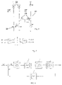
- FIG. 1 shows an exemplary embodiment of a transmitter which is based on current processing and uses differential path technology
- FIG. 2 shows a current amplifier using differential path technology, according to one refinement of the invention
- FIG. 3 shows one embodiment of a current filter
- FIG. 4 shows a level shifter, formed from current mirrors, according to one embodiment of the invention
- FIG. 5 shows a first exemplary embodiment of a voltage regulator for a current mirror
- FIG. 6 shows a further exemplary embodiment of a voltage regulator for a current mirror
- FIG. 7 shows a first exemplary embodiment of a feedback circuit for offset compensation
- FIG. 8 shows a simple equivalent circuit for calculation of the transmission characteristics in the frequency domain for the transmitter shown in FIG. 1 .
- FIG. 1 shows a schematic block diagram of a transmitter comprising a digital/analogue converter 1 , a form filter 2 , a current amplifier 3 , a level shifter 4 , and a line driver 5 .
- the elements 1 - 5 form the signal path of the transmitter.
- a circuit for offset compensation 6 with a low-pass filter characteristic, is provided in the feedback path 12 of the transmitter.
- a reference current production device 7 provides a reference current, which is supplied to all the units 1 - 6 . All the pulse currents as well as the currents for setting the operating point are thus derived from the reference current, thus avoiding undesirable offsets resulting from lack of synchronization. It is also feasible for the various components of the transmitter to be supplied with intrinsically independent currents. This must be decided on the basis of the requirements of bandwidths, linearity, etc.
- the reference current can additionally be adjusted in order to increase the accuracy of the pulse amplitude of the transmission pulses, and thus to guarantee compliance of specific pulse masks with various Standards.
- the digital/analogue converter 1 forms the input of the transmitter, and is in the form of a current-driving digital/analogue converter.
- the digital data which is supplied at the input is decoded in a decoder 13 , in order in this way to switch weighted current sources 14 .
- Internal regulation (not shown) ensures matching of the PNOS and NMOS current mirrors within the digital/analogue converter.
- Differential current pulses are produced at the outputs 15 of the D/A converter (comprising a DACP and a DACN), and are supplied to a current-controlled form filter 2 .
- the form filter 2 comprises a current divider 8 and a low-pass filter 9 , which provides desired pre-emphasis of the transmission pulses which are emitted at the output of the transmitter, and is at the same time used as a form filter for the DA current pulses.
- the current amplifier is in this case in the form of a divider 8 , which divides the amplitude of the arriving current pulses by a specific factor N. In this case, this is carried out only by way of example in order to reduce the power consumption or the surface area required for the downstream low-pass filter. It is also feasible for the signal current not be attenuated but to be amplified.
- the amplifier or divider stage 8 should in any case be designed to provide decoupling between the DA converter 1 and the filter 9 .
- a iv ⁇ ( s ) i out ⁇ ( s ) i in ⁇ ( s ) ⁇ gm N ⁇ ⁇ 1 gm N ⁇ ⁇ 2 * ( 1 1 + s * C N ⁇ ⁇ 1 gm N ⁇ ⁇ 1 ) ⁇ gm N ⁇ ⁇ 1 gm N ⁇ ⁇ 2 * ( 1 1 + s ⁇ iv ) [ 1.1 ]
- the subsequent low-pass filter 9 provides the desired signal forming and pre-emphasis, and preferably operates on the principle of GmC filtering.
- the transmission characteristic of the form-filter shown in FIG. 3 in the frequency domain is given by the following equation,
- a ltp ⁇ ( s ) ⁇ i out ⁇ ( s ) i in ⁇ ( s ) ⁇ R ⁇ ⁇ 1 R ⁇ ⁇ 2 * ( 1 + 1 gm N ⁇ ⁇ 1 * R ⁇ ⁇ 1 1 + 1 gm N ⁇ ⁇ 2 * R ⁇ ⁇ 2 ) ⁇ ( 1 1 + s * C N ⁇ ⁇ 1 ( gm N ⁇ ⁇ 1 + R ⁇ ⁇ 1 ) ) ⁇ ⁇ R ⁇ ⁇ 1 R ⁇ ⁇ 2 * ( 1 + 1 gm N ⁇ ⁇ 1 * R ⁇ ⁇ 1 1 + 1 gm N ⁇ ⁇ 2 * R ⁇ ⁇ 2 ) ⁇ ( 1 1 + s ⁇ ip ) [ 1.2 ] where
- the pre-emphasized current pulses are amplified by a specific factor N in the current amplifier 3 .
- the transfer function within the frequency domain is given by equation 1.1.
- the implementation of the current amplifier corresponds to FIG. 2 .
- the factor N is given by:
- a level shifter 4 is optionally connected to the output of the current amplifier 3 , transforms the supply voltage from a low supply voltage VDD 1 to a higher supply voltage VDD 2 and allows the circuit part which is located upstream of it to be operated with a lower supply voltage VDD 1 .
- This has the major advantage that it is possible to use transistors with a thinner gate oxide based on modern sub-micron technologies for the signal path. This is in turn evident in a higher speed and in a lower current consumption.
- the line driver 6 comprises an operational amplifier (OPV) with feedback resistors Rfb, by means of which the current pulses are converted to voltage pulses, as required for transmission.
- OOV operational amplifier
- Rfb feedback resistors
- the unit for the transfer function is Ohm [ ⁇ ].
- the transmission line 10 is terminated in a known manner by a line resistance RL.
- the offset compensation circuit 6 compensates for any DC offset between the outputs of the line drivers XL 1 and XL 2 .
- This circuit 6 is preferably formed from transconductance stages, and is fed back to the output 15 of the digital/analogue converter.
- the pole frequency should be below the lowest spectral component of the transmission pulses, and should have a corresponding low-pass filter characteristic.
- a fb ⁇ ( s ) i rfb ⁇ ( s ) v out ⁇ ( s ) ⁇ Gm ⁇ ⁇ 1 * R oGm ⁇ ⁇ 1 * Gm ⁇ ⁇ 2 * ( 1 1 + s * C fb Gm ⁇ ⁇ 1 + R oGm ⁇ ⁇ 1 ) ⁇ G ofb * ( 1 1 + s ⁇ fb ) ⁇ [ 1 ⁇ ] [ 1.5 ]
- FIG. 2 shows a simplified structure of a current amplifier 8 using differential path technology with mid-voltage regulation (Common Mode Feedback).
- the differential inputs of the current amplifier or divider are denoted INP and INN (P: Positive, N: Negative), and the corresponding outputs are denoted OUTP and OUTN.
- Each differential path comprises a current mirror 20 with mirror transistors N 1 , N 2 and N 1 ′, N 2 ′.
- the transfer function in equation 1.1 applies in the frequency domain to the current divider 8 shown in FIG. 1 .
- the staging ratio is given by:
- Mirror transistors N 1 , N 2 and N 1 ′ and N 2 ′ are each connected to a current source 22 , which supplies a current that is derived from the reference current I Ref .
- the inputs INP, INN of the current amplifier are clamped at a predetermined potential by DC voltage regulation 21 .
- the DC voltage regulation keeps the operating point of the current mirror 20 in a range which is as ideal as possible.
- the DC voltage regulation comprises a transistor P 1 or P 1 ′, which is connected between the respective differential input INP, INN and the respective mirror transistor N 1 , N 1 ′.
- FIG. 3 shows a current filter which is physically virtually identical to the current amplifier 8 shown in FIG. 2 .
- the current or form filter likewise comprises current mirrors 20 with mirror transistors N 1 , N 2 and N 1 ′, N 2 ′.
- the transistors P 1 and P 1 ′ regulate the input voltage at the nodes INP, INN.
- Degeneration resistors R 1 , R 2 and R 1 ′, R 2 ′, respectively, which increase the linear drive range, are connected to the source connections of the respective transistors N 1 , N 2 and N 1 ′, N 2 ′.
- the filtered response results from the sum of the degeneration resistance R 1 (R 1 ) and the reciprocal of the conductance of the transistor N 1 (N 1 ′) in parallel with the capacitance C (C′) which is connected to ground at the mirror point of the transistors N 1 , N 2 and N 1 ′, N 2 ′ respectively.
- the product of the resistance value and capacitance is proportional to the pole frequency of the filter.
- transistors N 2 and N 2 ′ form a parasitic pole by the diffusion capacitance at the drain connection, and this must be taken into account in the transmission characteristic.
- FIG. 4 shows a level shifter 4 , which is likewise formed from current mirrors 20 .
- the level shifter 4 is used for matching the different supply voltages VDD 1 , VDD 2 to the components in the signal path.
- the transistors N 1 , N 1 ′ and N 2 , N 2 ′ respectively form a current mirror, in the same way as the transistors P 2 , P 2 ′ and P 3 , P 3 ′.
- a cascode transistor N 3 (N 3 ′) is provided at the drain connection of the transistor N 2 , and must be suitable for a higher operating voltage.
- FIG. 5 shows one possible implementation of DC voltage regulation 21 with an operational amplifier 21 , whose inverted input is connected to the signal input of the stage, and whose non-inverted input is connected to a reference voltage.
- the output of the operation amplifier 23 is connected to the gate connection of the transistor P 1 .
- FIG. 6 shows another implementation of the voltage regulation 21 .
- the voltage regulation 21 comprises a current mirror 23 which is formed from the transistors P 4 and P 5 .
- a resistor R CM is provided at the source connection of the transistor P 5 .
- a current source I O is connected to the source connection of the transistor P 4 .
- the drain connection of the transistor P 5 is connected to a reference current source I REF .
- the transistor P 4 is connected to a current mirror 20 in one of the stages 2 - 4 described above. This circuitry results in a constant potential U 0 at the input.
- the voltage regulation can also be provided at the output of one of the stages 2 - 4 .
- FIG. 7 illustrates one possible implementation of the feedback circuit 6 for offset compensation.
- the feedback comprises a first transconductance stage Gm 1 , a second transconductance stage Gm 2 and a capacitance Cfb.
- the input nodes INP and INN are connected to the outputs XL 1 and XL 2 in the transmitter shown in FIG. 1 .
- the outputs OUTP and OUTN are connected to the connections DACN and DACP.
- the capacitance is connected between the outputs of the first transconductance Gm 1 and the inputs of the second transconductance Gm 2 .
- the dominant pole of the arrangement is formed from the quotient of the gradient of the first transconductance stage Gm 1 and of the capacitance Cfb.
- FIG. 8 shows a simplified illustration of the transmission chain in the transmitter shown in FIG. 1 .
- the transfer function from the output of the digital/analogue converter to the transmitter output is calculated taking into account the equations mentioned above as follows:
- the second harmonic distortion HD 2 can be chosen optimally by suitable choice of the bandwidth, by reduction of the parasitic mode capacitances, and by a suitable ratio of the signal current to the supply current for operating point adjustment.
- the individual components of the transmitter can be designed and implemented independently of the details of the practical implementation, with the aid of the stated equations, and, even if the internal supply voltage is low, they represent a stable and reliable implementation for pulse generation and transmission of data.
Landscapes
- Engineering & Computer Science (AREA)
- Power Engineering (AREA)
- Computer Networks & Wireless Communication (AREA)
- Signal Processing (AREA)
- Amplifiers (AREA)
- Dc Digital Transmission (AREA)
- Arrangements For Transmission Of Measured Signals (AREA)
Applications Claiming Priority (3)
| Application Number | Priority Date | Filing Date | Title |
|---|---|---|---|
| DE10125023A DE10125023A1 (de) | 2001-05-22 | 2001-05-22 | Transmitter zur Übertragung digitaler Daten über eine Übertragungsleitung |
| DE10125023.1 | 2001-05-22 | ||
| PCT/EP2002/005355 WO2002096050A2 (de) | 2001-05-22 | 2002-05-15 | Transmitter zur übertragung digitaler daten über eine übertragungsleitung |
Publications (2)
| Publication Number | Publication Date |
|---|---|
| US20040184558A1 US20040184558A1 (en) | 2004-09-23 |
| US7450649B2 true US7450649B2 (en) | 2008-11-11 |
Family
ID=7685789
Family Applications (1)
| Application Number | Title | Priority Date | Filing Date |
|---|---|---|---|
| US10/481,856 Expired - Lifetime US7450649B2 (en) | 2001-05-22 | 2003-05-15 | Current mode digital data transmitter |
Country Status (5)
| Country | Link |
|---|---|
| US (1) | US7450649B2 (de) |
| EP (1) | EP1389383B1 (de) |
| CN (1) | CN100544331C (de) |
| DE (2) | DE10125023A1 (de) |
| WO (1) | WO2002096050A2 (de) |
Cited By (3)
| Publication number | Priority date | Publication date | Assignee | Title |
|---|---|---|---|---|
| US20020188957A1 (en) * | 2001-06-08 | 2002-12-12 | Jantzi Stephen A. | Integrated upstream amplifier for cable modems and cable set-top boxes |
| US20120200960A1 (en) * | 2008-08-19 | 2012-08-09 | Sma Solar Technology Ag | Method for measuring a current, in particular by means of a grounding apparatus |
| US9160309B2 (en) | 2013-12-11 | 2015-10-13 | Qualcomm Incorporated | Area efficient baseband filter |
Families Citing this family (5)
| Publication number | Priority date | Publication date | Assignee | Title |
|---|---|---|---|---|
| US7155164B1 (en) | 2004-06-03 | 2006-12-26 | Marvell International Ltd. | Method and apparatus for performing transmit pre-emphasis |
| WO2008064515A1 (fr) * | 2006-11-27 | 2008-06-05 | Hisfan Chang | Filtre approprié à une extrémité de service client en boucle dsl |
| FR3024306B1 (fr) * | 2014-07-23 | 2018-03-30 | Devialet | Convertisseur courant-tension, etage d'entree d'un amplificateur et amplificateur correspondant |
| FR3024305B1 (fr) * | 2014-07-23 | 2018-03-30 | Devialet | Etage d'entree d'un amplificateur et amplificateur correspondant |
| US9780777B1 (en) * | 2016-04-04 | 2017-10-03 | Mediatek Inc. | Methods and apparatus for level-shifting high speed serial data with low power consumption |
Citations (7)
| Publication number | Priority date | Publication date | Assignee | Title |
|---|---|---|---|---|
| US3946303A (en) * | 1973-04-28 | 1976-03-23 | Robert Bosch Gmbh | Monolithic integrated voltage regulator |
| US5504782A (en) | 1994-07-29 | 1996-04-02 | Motorola Inc. | Current mode transmitter and receiver for reduced RFI |
| EP0963083A2 (de) | 1998-06-02 | 1999-12-08 | Fujitsu Limited | Verfahren und Einrchtung zur richtigen Signalübertragung mit hoher Geschwindigkeit und ohne Wellenformverzerrung |
| US6154784A (en) * | 1998-06-10 | 2000-11-28 | Lsi Logic Corporation | Current mode ethernet transmitter |
| GB2354125A (en) | 1999-09-09 | 2001-03-14 | Ericsson Telefon Ab L M | A TDMA transmitter with feedback power control loop offset compensation |
| US6282042B1 (en) * | 1996-09-24 | 2001-08-28 | Hewlett-Packard Company | Data processing apparatus and methods |
| US6577197B1 (en) * | 2001-11-06 | 2003-06-10 | National Semiconductor Corporation | High frequency compensation circuit for high frequency amplifiers |
-
2001
- 2001-05-22 DE DE10125023A patent/DE10125023A1/de not_active Ceased
-
2002
- 2002-05-15 CN CNB02811275XA patent/CN100544331C/zh not_active Expired - Fee Related
- 2002-05-15 DE DE50201238T patent/DE50201238D1/de not_active Expired - Lifetime
- 2002-05-15 EP EP02730256A patent/EP1389383B1/de not_active Expired - Lifetime
- 2002-05-15 WO PCT/EP2002/005355 patent/WO2002096050A2/de not_active Ceased
-
2003
- 2003-05-15 US US10/481,856 patent/US7450649B2/en not_active Expired - Lifetime
Patent Citations (7)
| Publication number | Priority date | Publication date | Assignee | Title |
|---|---|---|---|---|
| US3946303A (en) * | 1973-04-28 | 1976-03-23 | Robert Bosch Gmbh | Monolithic integrated voltage regulator |
| US5504782A (en) | 1994-07-29 | 1996-04-02 | Motorola Inc. | Current mode transmitter and receiver for reduced RFI |
| US6282042B1 (en) * | 1996-09-24 | 2001-08-28 | Hewlett-Packard Company | Data processing apparatus and methods |
| EP0963083A2 (de) | 1998-06-02 | 1999-12-08 | Fujitsu Limited | Verfahren und Einrchtung zur richtigen Signalübertragung mit hoher Geschwindigkeit und ohne Wellenformverzerrung |
| US6154784A (en) * | 1998-06-10 | 2000-11-28 | Lsi Logic Corporation | Current mode ethernet transmitter |
| GB2354125A (en) | 1999-09-09 | 2001-03-14 | Ericsson Telefon Ab L M | A TDMA transmitter with feedback power control loop offset compensation |
| US6577197B1 (en) * | 2001-11-06 | 2003-06-10 | National Semiconductor Corporation | High frequency compensation circuit for high frequency amplifiers |
Non-Patent Citations (1)
| Title |
|---|
| Bouras, S., T. Georgantas, Y. Papananos, and D. Dervenis, "Current Mode Baseband Interface for Communication Applications," National Technical University of Athens, (C) 1999, (4 pages). |
Cited By (7)
| Publication number | Priority date | Publication date | Assignee | Title |
|---|---|---|---|---|
| US20020188957A1 (en) * | 2001-06-08 | 2002-12-12 | Jantzi Stephen A. | Integrated upstream amplifier for cable modems and cable set-top boxes |
| US8013768B2 (en) * | 2001-06-08 | 2011-09-06 | Broadcom Corporation | Integrated upstream amplifier for cable modems and cable set-top boxes |
| US20120086592A1 (en) * | 2001-06-08 | 2012-04-12 | Broadcom Corporation | Integrated Upstream Amplifier for Cable Modem and Cable Set-Top Boxes |
| US8334721B2 (en) * | 2001-06-08 | 2012-12-18 | Broadcom Corporation | Integrated upstream amplifier for cable modem and cable set-top boxes |
| US20120200960A1 (en) * | 2008-08-19 | 2012-08-09 | Sma Solar Technology Ag | Method for measuring a current, in particular by means of a grounding apparatus |
| US8717047B2 (en) * | 2008-08-19 | 2014-05-06 | Sma Solar Technology Ag | Method for measuring a current, in particular by means of a grounding apparatus |
| US9160309B2 (en) | 2013-12-11 | 2015-10-13 | Qualcomm Incorporated | Area efficient baseband filter |
Also Published As
| Publication number | Publication date |
|---|---|
| WO2002096050A2 (de) | 2002-11-28 |
| CN100544331C (zh) | 2009-09-23 |
| US20040184558A1 (en) | 2004-09-23 |
| CN1611046A (zh) | 2005-04-27 |
| EP1389383B1 (de) | 2004-10-06 |
| DE50201238D1 (de) | 2004-11-11 |
| DE10125023A1 (de) | 2002-12-12 |
| WO2002096050A3 (de) | 2003-06-12 |
| EP1389383A2 (de) | 2004-02-18 |
Similar Documents
| Publication | Publication Date | Title |
|---|---|---|
| US6037841A (en) | Impedance matched CMOS transimpedance amplifier for high-speed fiber optic communications | |
| US5166635A (en) | Digital data line driver | |
| US8598906B2 (en) | Low-power ethernet transmitter | |
| US5844442A (en) | Low voltage fully differential operational amplifier with improved common mode circuitry | |
| US7626424B2 (en) | Wireline transmission circuit | |
| JP3272380B2 (ja) | 高性能演算増幅器と増幅方法 | |
| EP1168740A2 (de) | Leitungstreiber mit adaptiver Impedanz | |
| JPH09130169A (ja) | 単終端入力を差動出力信号に変換するためのコンバータ、入力により差動出力信号を発生する方法、および差動入力電圧を単終端出力電圧に変換するためのコンバータ | |
| US6507223B2 (en) | Differential line driver having adjustable common mode operation | |
| TWI740539B (zh) | 藉助於差動漂移電流感測來進行基線漂移修正的裝置 | |
| US7450649B2 (en) | Current mode digital data transmitter | |
| US6580760B1 (en) | Line drive architecture with programmable gain and drive | |
| US7127061B2 (en) | Line driver for digital signal transmission | |
| CN111865339A (zh) | 传送器、接收器及混合式收发器 | |
| EP1434348A1 (de) | Breitband-Gleichtaktregler | |
| KR100766477B1 (ko) | 인체를 이용한 통신채널에서의 광대역 펄스신호 수신장치 | |
| US7212038B2 (en) | Line driver for transmitting data | |
| EP0864208B1 (de) | Cmos-übertragungsleitungsentzerrer | |
| JP3875726B2 (ja) | フィルタ及び発振器用の相補トランスコンダクタを具えている電子回路 | |
| KR20230140255A (ko) | 차동 출력 신호의 오프셋 보상이 가능한 차동 증폭기 및 이를 포함하는 적응형 연속 시간 선형 등화기 | |
| US20030076080A1 (en) | Linear power conversion circuit | |
| US6470084B1 (en) | Current amplifier, particularly for a telephone line | |
| JP3931025B2 (ja) | 自己バイアス調整回路 | |
| JP3830534B2 (ja) | 適応出力インピーダンスを有するラインドライバ | |
| JP3830535B2 (ja) | 適応出力インピーダンスを有するラインドライバ |
Legal Events
| Date | Code | Title | Description |
|---|---|---|---|
| AS | Assignment |
Owner name: INFINEON TECHNOLOGIES AG, GERMANY Free format text: ASSIGNMENT OF ASSIGNORS INTEREST;ASSIGNORS:GREGORIUS, PETER;HANNEBERG, ARMIN;REEL/FRAME:015364/0986 Effective date: 20031127 |
|
| STCF | Information on status: patent grant |
Free format text: PATENTED CASE |
|
| CC | Certificate of correction | ||
| AS | Assignment |
Owner name: INFINEON TECHNOLOGIES WIRELESS SOLUTIONS GMBH,GERM Free format text: ASSIGNMENT OF ASSIGNORS INTEREST;ASSIGNOR:INFINEON TECHNOLOGIES AG;REEL/FRAME:024483/0021 Effective date: 20090703 Owner name: INFINEON TECHNOLOGIES WIRELESS SOLUTIONS GMBH, GER Free format text: ASSIGNMENT OF ASSIGNORS INTEREST;ASSIGNOR:INFINEON TECHNOLOGIES AG;REEL/FRAME:024483/0021 Effective date: 20090703 |
|
| AS | Assignment |
Owner name: LANTIQ DEUTSCHLAND GMBH,GERMANY Free format text: ASSIGNMENT OF ASSIGNORS INTEREST;ASSIGNOR:INFINEON TECHNOLOGIES WIRELESS SOLUTIONS GMBH;REEL/FRAME:024529/0593 Effective date: 20091106 Owner name: LANTIQ DEUTSCHLAND GMBH, GERMANY Free format text: ASSIGNMENT OF ASSIGNORS INTEREST;ASSIGNOR:INFINEON TECHNOLOGIES WIRELESS SOLUTIONS GMBH;REEL/FRAME:024529/0593 Effective date: 20091106 |
|
| AS | Assignment |
Owner name: DEUTSCHE BANK AG NEW YORK BRANCH, AS COLLATERAL AG Free format text: GRANT OF SECURITY INTEREST IN U.S. PATENTS;ASSIGNOR:LANTIQ DEUTSCHLAND GMBH;REEL/FRAME:025406/0677 Effective date: 20101116 |
|
| FEPP | Fee payment procedure |
Free format text: PAYOR NUMBER ASSIGNED (ORIGINAL EVENT CODE: ASPN); ENTITY STATUS OF PATENT OWNER: LARGE ENTITY |
|
| FPAY | Fee payment |
Year of fee payment: 4 |
|
| AS | Assignment |
Owner name: LANTIQ BETEILIGUNGS-GMBH & CO. KG, GERMANY Free format text: RELEASE OF SECURITY INTEREST RECORDED AT REEL/FRAME 025413/0340 AND 025406/0677;ASSIGNOR:DEUTSCHE BANK AG NEW YORK BRANCH, AS COLLATERAL AGENT;REEL/FRAME:035453/0712 Effective date: 20150415 |
|
| FPAY | Fee payment |
Year of fee payment: 8 |
|
| AS | Assignment |
Owner name: LANTIQ BETEILIGUNGS-GMBH & CO. KG, GERMANY Free format text: MERGER AND CHANGE OF NAME;ASSIGNORS:LANTIQ DEUTSCHLAND GMBH;LANTIQ BETEILIGUNGS-GMBH & CO. KG;REEL/FRAME:045086/0015 Effective date: 20150303 |
|
| MAFP | Maintenance fee payment |
Free format text: PAYMENT OF MAINTENANCE FEE, 12TH YEAR, LARGE ENTITY (ORIGINAL EVENT CODE: M1553); ENTITY STATUS OF PATENT OWNER: LARGE ENTITY Year of fee payment: 12 |
|
| AS | Assignment |
Owner name: INTEL CORPORATION, CALIFORNIA Free format text: ASSIGNMENT OF ASSIGNORS INTEREST;ASSIGNOR:LANTIQ BETEILIGUNGS-GMBH & CO. KG;REEL/FRAME:053259/0678 Effective date: 20200710 |
|
| AS | Assignment |
Owner name: MAXLINEAR, INC., CALIFORNIA Free format text: ASSIGNMENT OF ASSIGNORS INTEREST;ASSIGNOR:INTEL CORPORATION;REEL/FRAME:053626/0636 Effective date: 20200731 |
|
| AS | Assignment |
Owner name: WELLS FARGO BANK, NATIONAL ASSOCIATION, COLORADO Free format text: SECURITY AGREEMENT;ASSIGNORS:MAXLINEAR, INC.;MAXLINEAR COMMUNICATIONS, LLC;EXAR CORPORATION;REEL/FRAME:056816/0089 Effective date: 20210708 |