US7296934B2 - Optical transmission module and manufacturing method thereof - Google Patents
Optical transmission module and manufacturing method thereof Download PDFInfo
- Publication number
- US7296934B2 US7296934B2 US11/068,677 US6867705A US7296934B2 US 7296934 B2 US7296934 B2 US 7296934B2 US 6867705 A US6867705 A US 6867705A US 7296934 B2 US7296934 B2 US 7296934B2
- Authority
- US
- United States
- Prior art keywords
- optical
- optical element
- transmission module
- connection parts
- reinforcement
- Prior art date
- Legal status (The legal status is an assumption and is not a legal conclusion. Google has not performed a legal analysis and makes no representation as to the accuracy of the status listed.)
- Expired - Fee Related, expires
Links
Images


Classifications
-
- G—PHYSICS
- G02—OPTICS
- G02B—OPTICAL ELEMENTS, SYSTEMS OR APPARATUS
- G02B6/00—Light guides; Structural details of arrangements comprising light guides and other optical elements, e.g. couplings
- G02B6/24—Coupling light guides
- G02B6/26—Optical coupling means
- G02B6/30—Optical coupling means for use between fibre and thin-film device
-
- G—PHYSICS
- G02—OPTICS
- G02B—OPTICAL ELEMENTS, SYSTEMS OR APPARATUS
- G02B6/00—Light guides; Structural details of arrangements comprising light guides and other optical elements, e.g. couplings
- G02B6/10—Light guides; Structural details of arrangements comprising light guides and other optical elements, e.g. couplings of the optical waveguide type
- G02B6/12—Light guides; Structural details of arrangements comprising light guides and other optical elements, e.g. couplings of the optical waveguide type of the integrated circuit kind
- G02B2006/12035—Materials
- G02B2006/12069—Organic material
-
- G—PHYSICS
- G02—OPTICS
- G02B—OPTICAL ELEMENTS, SYSTEMS OR APPARATUS
- G02B6/00—Light guides; Structural details of arrangements comprising light guides and other optical elements, e.g. couplings
- G02B6/10—Light guides; Structural details of arrangements comprising light guides and other optical elements, e.g. couplings of the optical waveguide type
- G02B6/12—Light guides; Structural details of arrangements comprising light guides and other optical elements, e.g. couplings of the optical waveguide type of the integrated circuit kind
- G02B2006/12133—Functions
- G02B2006/1215—Splitter
-
- G—PHYSICS
- G02—OPTICS
- G02B—OPTICAL ELEMENTS, SYSTEMS OR APPARATUS
- G02B6/00—Light guides; Structural details of arrangements comprising light guides and other optical elements, e.g. couplings
- G02B6/10—Light guides; Structural details of arrangements comprising light guides and other optical elements, e.g. couplings of the optical waveguide type
- G02B6/12—Light guides; Structural details of arrangements comprising light guides and other optical elements, e.g. couplings of the optical waveguide type of the integrated circuit kind
- G02B2006/12166—Manufacturing methods
- G02B2006/1219—Polymerisation
Abstract
An optical transmission module is disclosed that comprises an optical element having an optical path formed therein, optical connection parts respectively arranged on both sides of the optical element so as to connect the optical element to plural optical fibers, and reinforcement parts. The reinforcement parts are applied to a part of or an entire circumference of respective connected portions between the optical element and the optical connection parts, and then cured to reinforce connections between the optical element and the optical connection parts.
Description
1. Field of the Invention
The present invention relates to an optical transmission module and a manufacturing method thereof, and particularly relates to an optical transmission module having an optical element with an optical circuit formed therein and optical connection parts adapted to connect optical fibers to the optical element.
2. Description of the Related Art
In recent years, with a rapid progress in optical communications, enhancement of communication speed and transmission capacity has been promoted. Wavelength-Division Multiplexing (WDM), which is a multiplexing technique using lights with various wavelengths and capable of supporting such enhancement, is gaining widespread use in optical communication systems. The WDM requires highly-accurate optical components for enabling multiplexing and demultiplexing of lights with a wavelength interval of 1 nm or less.
As is commonly known in the art of optical communications, various optical elements are used in transmission channels formed by optical fibers (see, for example, Japanese Patent Laid-Open Publication No. 05-264862). Among the optical components, waveguide components are remarkable in that they are mass-producible and applicable to LSI. Especially, expectations for Planar Lightwave Circuit (PLC), which is one of the waveguide components, is high because it can be connected to optical fibers with a low optical transmission loss and can integrate a number of optical functions therein.
A PLC substrate having such a PLC optically connected to optical fibers is therefore used in high-speed and large-capacity optical communications. The PLC substrate is connected to the optical fibers by fiber arrays, and the fiber arrays are connected to the PLC substrate by optical path forming resins.
Conventionally, the optical elements having PLCs have been made of quartz, Pyrex (™), or the like. However, with recent developments for size and weight reduction and easier production, the core and cladding of optical elements having PLCs can be formed by laminating polymer resins with different refractive indexes on a silicon substrate.
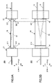
The optical transmission module 10 comprises an optical element 30, and fiber arrays 21 and 22 for connecting optical fibers 11, 12 and 13 to the optical element 30.
The fiber array 21 holds the optical fiber 11, an end face of which is exposed from an end face of the fiber array 21 in the direction of an arrow X2. The fiber array 22 holds the optical fibers 12 and 13, an end face of each of which is exposed from an end face of the fiber array 22 in the direction of an arrow X1. The fiber arrays 21 and 22 are typically made of quartz or a glass material. The end face of the fiber array 21 in the direction of the arrow X2 is bonded to the optical element 30 through an optical path forming resin 41 so as to match the end face of the optical fiber 11 and an end face of an optical path formed in the optical element 30. The end face of the fiber array 22 in the direction of the arrow X1 is bonded to the optical element 30 through an optical path forming resin 42 so as to match the end faces of the optical fibers 12 and 13 and end faces of optical paths formed in the optical element 30.
The following describes the optical element 30 in detail.
The optical element 30 is adapted to branch an incident light output and output branched lights form a waveguide, comprising a substrate 31, a lower cladding layer 32, a core 33, and an upper cladding layer 34. The substrate 31 is, for example, a silicon (Si) substrate. The lower cladding layer 32, the core 33, the upper cladding layer 34 are resin laminations formed on the substrate 31.
The following describes a manufacturing method of the optical element 30.
First, the lower cladding layer 32 is formed on the substrate 31. The lower cladding layer 32 is typically made of transparent resin such as fluorinated polyimide. The lower cladding layer 32 is formed by, for example, forming a polyamic acid layer on the substrate 31 with a spin-coating method, and imidizing the layer through a heat treatment.
Then, the core 33 is formed on the lower cladding layer 32. The core 33 as a waveguide is made of the same fluorinated polyimide as the lower cladding layer 32 and the upper cladding layer 34. The composition of the resin of the core 33 is adjusted to have a refractive index different from that of the lower cladding layer 32 and the upper cladding layer 34. For example, when the refractive index of the lower cladding layer 32 and the upper cladding layer 34 is n1 and the refractive index of the core 33 is n2, the composition of the resin is adjusted to have
n1<n2.
Herein, the refractive index n1 and n2 are, for example, n1=1.525, n2=1.531.
n1<n2.
Herein, the refractive index n1 and n2 are, for example, n1=1.525, n2=1.531.
For forming the core 33, a polyamic acid layer is formed uniformly on the lower cladding layer 32 with a spin-coating method, and the layer is imidized through a heat treatment to form a transparent resin layer. Then, the transparent resin layer is coated with a patterned resist, and is dry-etched by a RIE (Reactive Ion Etching) machine to have the lower cladding layer 32 exposed. In this process, a part coated with a photoresist remains unetched to keep the transparent resin layer thereunder. Then, the remaining photoresist is removed. In this way, the core 33 with a desired pattern is formed. The thickness of the core 33 is around 9 through 10 μm, which is substantially equal to the diameter of the optical fibers 11, 12 and 13.
Next, the upper cladding layer 34 is formed to cover the upper and side surfaces of the core 33. The upper cladding layer 34 is made of the same fluorinated polyimide as the lower cladding layer 32, and the composition thereof is adjusted to have the refractive index n1, which is the same refractive index as the lower cladding layer 32. The upper cladding layer 34 is formed by, for example, forming a polyamic acid layer with a spin-coating method, and imidizing the layer through a heat treatment.
In this way, the optical element 30 having a waveguide with a desired pattern is formed.
The optical element 30 having polymer resins with different refractive indexes on the silicon substrate cannot have a resin material on the upper, side, and bottom surfaces thereof due to a large influence of the refractive index. If the optical element 30 has the resin material on those surfaces, a light passing through the core 33 is lost. For this reason, the optical element 30 is connected to the fiber arrays 21 and 22 only at the end faces thereof.
However, the end faces of the optical element 30 are small, so that the connection areas between the optical element 30 and the fiber arrays 21 and 22 are also small. This makes connections between the optical element 30 and the fiber arrays 21 and 22 weak. Therefore, the optical transmission module 10 with a silicon substrate described above is disadvantageous in this respect.
An object of the present invention is to provide an optical transmission module and a manufacturing method thereof to overcome at least one disadvantage described above. The specific object of the present invention is to provide an optical transmission module and a manufacturing method thereof to strengthen connections between fiber arrays and an optical element with minimum optical loss.
According to an aspect of the present invention, there is provided an optical transmission module, comprising an optical element having an optical path formed therein, optical connection parts respectively arranged on both sides of the optical element so as to connect the optical element to plural optical fibers, and reinforcement parts applied to a part of or an entire circumference of respective connected portions between the optical element and the optical connection parts and cured to reinforce connections between the optical element and the optical connection parts.
The reinforcement parts are preferably made of a resin material with hardness lower than the hardness of a material of the optical element, a material of the optical connection parts, and an optical path forming resin connecting the optical element and the optical connection parts.
It is preferable that the Young's modulus of the resin material of the reinforcement parts be approximately 9.0×10⁹ or lower.
It is also preferable that the Young's modulus of the resin materials of the reinforcement parts be approximately 1.0×10⁴ or higher.
It is also preferable that the reinforcement parts be respectively formed as fillets on the corresponding connected portions between the optical element and the optical connection parts.
According to another aspect of the present invention, there is provided a manufacturing method of an optical transmission module including an optical element having an optical path formed therein, and optical connection parts respectively arranged on both sides of the optical element so as to connect the optical element to plural optical fibers. The method comprises a connecting step of connecting the optical element to the optical connection parts by an optical path forming resin, and a reinforcing step of applying a resin to a part of or an entire circumference of connected portions between the optical element and the optical connection parts and curing the resin to reinforce connections between the optical element and the optical connection parts, after the connecting step in which the optical element and the optical connection parts are connected by the optical path forming resin.
According to the present invention, since there are reinforcement parts applied to a part of or an entire circumference of the respective connected portions between the optical element and the optical connection parts and cured to reinforce connections between the optical element and the optical connection parts, the connections between the optical element and the optical connection parts can be reinforced with minimum optical loss.
The optical transmission module 100 according to the first embodiment has a fillet-like reinforcement portion 111 around a connected portion between the fiber array 21 and the optical element 30, and a reinforcement portion 112 around a connected portion between the fiber array 22 and the optical element 30. The fiber arrays 21 and 22 correspond to optical connection parts in the following claims.
The reinforcement portion 111 is made of a resin material, such as a silicon-based resin material, with hardness lower than the resin material of the optical element 30, the resin material of the fiber array 21, and the optical path forming resin 41 connecting the optical element 30 to the fiber array 21.
The optical loss has the characteristic as shown in FIG. 3 in relation to Young's modulus of the reinforcement portions 111 and 112. For example, it was found from experiment that the optical loss at the connected portions between the optical element 30 and the fiber arrays 21 and 22 is reduced when a resin material with the Young's modulus in a cured state of approximately 1.0×10⁴ through 9.0×10⁹ is used as the resin material of the reinforcement portions 111 and 112.
According to the first embodiment, the connection between the fiber arrays 21 and 22 and the optical element 30 is strengthened by forming the fillet- like reinforcement portions 111 and 112 around the connected portions between the fiber arrays 21 and 22 and the optical element 30. Especially, the optical loss is minimized when a silicon-based resin with the Young's modulus in a cured state of approximately 1.0×10⁴ through 9.0×10⁹ is used as the reinforcement portions 111 and 112.
The following describes a manufacturing method of the optical transmission module 100 of the first embodiment.
First, the end face of the optical element 30 in the direction of the arrow X1 and the fiber array 21 are connected through the optical path forming resin 41 so as to match the optical paths thereof, and the optical path forming resin 41 is cured. Likewise, the end face of the optical element 30 in the direction of the arrow X2 and the fiber array 22 are connected through the optical path forming resin 42 so as to match the optical paths thereof, and the optical path forming resin 42 is cured. The fiber arrays 21 and 22 are thus bonded to the optical element 30 respectively at the end faces in the directions of the arrow X1 and the arrow X2.
Next, a reinforcement resin material is applied to the entire circumference of the connected portion between the end face of the optical element 30 in the direction of the arrow X1 and the fiber array 21, and cured through addition/condensation reactions by, for example, a heat treatment and an ultraviolet radiation to form the reinforcement portion 111. Likewise, a reinforcement resin material is applied to the entire circumference of the connected portion between the end face of the optical element 30 in the direction of the arrow X2 and the fiber array 22, and is cured through addition/condensation reactions by, for example, a heat treatment and an ultraviolet radiation to form the reinforcement portion 112. In this way, the reinforcement portions 111 and 112 are respectively formed on the entire circumferences of the connected portions between the end faces of the optical element 30 in the directions of the arrows X1 and X2 and the fiber arrays 21 and 22.
Since the reinforcement portions 111 and 112 formed on the connected portions between the optical element 30 and the fiber arrays 21 and 22 are made of the resin material with hardness that minimizes the optical loss, i.e., with the Young's modulus of approximately 1.0×10⁴ through 9.0×10⁹, the connections between the optical element 30 and the fiber arrays 21 and 22 are strengthened while minimizing the optical loss at the connected portions between the optical element 30 and the fiber arrays 21 and 22 and therearound.
The optical transmission module 200 of the second embodiment is different from that of the first embodiment in the position of reinforcement portions 211, 212, 221 and 222.
The reinforcement portion 211 is made of a resin material with the Young's modulus in a cured state of approximately 1.0×10⁴ through 9.0×10⁹, which is applied and cured like a fillet on the edges of the optical element 30 and the fiber array 21 in the direction of an arrow Z1. The reinforcement portion 212 is made of a resin material with the Young's modulus in a cured state of approximately 1.0×10⁴ through 9.0×10⁹, which is applied and cured like a fillet on the edges of the optical element 30 and the fiber array 21 in the direction of an arrow Z2.
The reinforcement portion 221 is made of a resin material with the Young's modulus in a cured state of approximately 1.0×10⁴ through 9.0×10⁹, which is applied and cured like a fillet on the edges of the optical element 30 and the fiber array 22 in the direction of the arrow Z1. The reinforcement portion 222 is made of a resin material with the Young's modulus in a cured state of approximately 1.0×10⁴ through 9.0×10⁹, which is applied and cured like a fillet on the edges of the optical element 30 and the fiber array 22 in the direction of the arrow Z2.
According to the second embodiment, since the reinforcement portions 211, 212, 221 and 222 are formed only on the edges of the optical element 30 and the fiber arrays 21 and 22 in the directions of the arrows Z1 and Z2, the optical loss at the connected portions between the optical element 30 and the fiber arrays 21 and 22 is reduced.
The optical transmission module 300 of the third embodiment is different from those of the first and second embodiments in the position of reinforcement portions 311, 312, 321 and 322.
The reinforcement portion 311 is made of a resin material with the Young's modulus in a cured state of approximately 1.0×10⁴ through 9.0×10⁹, which is applied and cured like a fillet on the edges of the optical element 30 and the fiber array 21 in the direction of an arrow Y1. The reinforcement portion 312 is made of a resin material with the Young's modulus in a cured state of approximately 1.0×10⁴ through 9.0×10⁹, which is applied and cured like a fillet on the edges of the optical element 30 and the fiber array 21 in the direction of an arrow Y2.
The reinforcement portion 321 is made of a resin material with the Young's modulus in a cured state of approximately 1.0×10⁴ through 9.0×10⁹, which is applied and cured like a fillet on the edges of the optical element 30 and the fiber array 22 in the direction of the arrow Y1. The reinforcement portion 322 is made of a resin material with the Young's modulus in a cured state of approximately 1.0×10⁴ through 9.0×10⁹, which is applied and cured like a fillet on the edges of the optical element 30 and the fiber array 22 in the direction of the arrow Y2.
According to the third embodiment, since the reinforcement portions 311, 312, 321 and 322 are formed only on the edges of the optical element 30 and the fiber arrays 21 and 22 in the directions of the arrows Y1 and Y2, the optical loss at the connected portions between the optical element 30 and the fiber arrays 21 and 22 is reduced.
While the optical element 30 that branches a light into two is exemplified in the above embodiments, the present invention is applicable to other types of optical elements without being limited to the above specific optical element 30.
The present application is based on Japanese Priority Application No. 2004-325087 filed on Nov. 9, 2004, with the Japanese Patent Office, the entire contents of which are hereby incorporated by reference.
Claims (6)
1. An optical transmission module, comprising:
an optical element having an optical path formed therein;
optical connection parts respectively arranged on both sides of the optical element so as to connect the optical element to a plurality of optical fibers; and
reinforcement parts applied to a part of or an entire circumference of respective connected portions between the optical element and the optical connection parts and cured to reinforce connections between the optical element and the optical connection parts.
2. The optical transmission module as claimed in claim 1 , wherein the reinforcement parts are made of a resin material with hardness lower than hardness of a material of the optical element, a material of the optical connection parts, and an optical path forming resin connecting the optical element and the optical connection parts.
3. The optical transmission module as claimed in claim 2 , wherein the Young's modulus of the resin material of the reinforcement parts is approximately 9.0×10⁹ or lower.
4. The optical transmission module as claimed in claim 3 , wherein the Young's modulus of the resin materials of the reinforcement parts is approximately 1.0×10⁴ or higher.
5. The optical transmission module as claimed in claim 1 , wherein the reinforcement parts are respectively formed as fillets on the corresponding connected portions between the optical element and the optical connection parts.
6. A manufacturing method of an optical transmission module including an optical element having an optical path formed therein, and optical connection parts respectively arranged on both sides of the optical element so as to connect the optical element to a plurality of optical fibers, comprising:
a connecting step of connecting the optical element to the optical connection parts by an optical path forming resin; and
a reinforcing step of applying a resin to a part of or an entire circumference of connected portions between the optical element and the optical connection parts and curing the resin to reinforce connections between the optical element and the optical connection parts, after the connecting step in which the optical element and the optical connection parts are connected by the optical path forming resin.
Applications Claiming Priority (2)
| Application Number | Priority Date | Filing Date | Title |
|---|---|---|---|
| JP2004325087A JP2006133666A (en) | 2004-11-09 | 2004-11-09 | Optical transmission module and method for manufacturing the same |
| JP2004-325087 | 2004-11-09 |
Publications (2)
| Publication Number | Publication Date |
|---|---|
| US20060098920A1 US20060098920A1 (en) | 2006-05-11 |
| US7296934B2 true US7296934B2 (en) | 2007-11-20 |
Family
ID=36316412
Family Applications (1)
| Application Number | Title | Priority Date | Filing Date |
|---|---|---|---|
| US11/068,677 Expired - Fee Related US7296934B2 (en) | 2004-11-09 | 2005-02-28 | Optical transmission module and manufacturing method thereof |
Country Status (3)
| Country | Link |
|---|---|
| US (1) | US7296934B2 (en) |
| JP (1) | JP2006133666A (en) |
| CN (1) | CN100514100C (en) |
Cited By (1)
| Publication number | Priority date | Publication date | Assignee | Title |
|---|---|---|---|---|
| US20060291782A1 (en) * | 2005-06-24 | 2006-12-28 | 3M Innovative Properties Company | Optical device with cantilevered fiber array and planar lightwave circuit |
Families Citing this family (3)
| Publication number | Priority date | Publication date | Assignee | Title |
|---|---|---|---|---|
| JP5498175B2 (en) * | 2010-01-06 | 2014-05-21 | アンリツ株式会社 | Optical coupling device |
| CN108345065B (en) * | 2017-01-24 | 2020-04-14 | 华为技术有限公司 | Optical signal processing device and preparation method |
| JP2022135003A (en) * | 2021-03-04 | 2022-09-15 | 住友電気工業株式会社 | optical connector cable |
Citations (7)
| Publication number | Priority date | Publication date | Assignee | Title |
|---|---|---|---|---|
| US4805981A (en) * | 1984-11-15 | 1989-02-21 | British Telecommunications, Plc | Telecommunications cable containing optical fibers |
| US5214730A (en) * | 1991-05-13 | 1993-05-25 | Nippon Telegraph And Telephone Corporation | Multifiber optical connector plug with low reflection and low insertion loss |
| JPH05264862A (en) | 1992-03-18 | 1993-10-15 | Furukawa Electric Co Ltd:The | Optical waveguide module |
| US5555332A (en) * | 1995-06-08 | 1996-09-10 | Siecor Corporation | Applicator and associated method for inserting guide pins in a fiber optic connector |
| US6198865B1 (en) * | 1999-08-13 | 2001-03-06 | Alcatel | Telecommunications cable having good adhesion between a protective jacket and strength members |
| US20030068153A1 (en) * | 2001-05-30 | 2003-04-10 | Ngk Insulators, Ltd. | Microhole array, optical fiber array, connector, and microhole array manufacturing method |
| US6565261B1 (en) * | 1999-02-22 | 2003-05-20 | Seiko Instruments Inc. | Optical fiber connector |
Family Cites Families (9)
| Publication number | Priority date | Publication date | Assignee | Title |
|---|---|---|---|---|
| JPS63205617A (en) * | 1987-02-20 | 1988-08-25 | Fujitsu Ltd | Structure of waveguide type optical device |
| JPH0273207A (en) * | 1988-09-09 | 1990-03-13 | Nippon Telegr & Teleph Corp <Ntt> | Packaging structure of optical waveguide parts |
| JPH02304405A (en) * | 1989-05-18 | 1990-12-18 | Sumitomo Metal Mining Co Ltd | Optical fiber holder and connecting method for optical fiber using same |
| JP3194397B2 (en) * | 1991-08-05 | 2001-07-30 | 日本電信電話株式会社 | Optical waveguide circuit module |
| JPH0886933A (en) * | 1994-09-16 | 1996-04-02 | Hitachi Cable Ltd | Optical waveguide module |
| JP3137168B2 (en) * | 1994-10-20 | 2001-02-19 | 日本電信電話株式会社 | Optical waveguide module |
| KR100357853B1 (en) * | 2000-12-30 | 2002-10-25 | 삼성전자 주식회사 | Plannar light waveguide circuit element using landmark |
| KR100442604B1 (en) * | 2001-12-27 | 2004-08-02 | 삼성전자주식회사 | Optical fiber block with reinforcing sub-block |
| JP2004029632A (en) * | 2002-06-28 | 2004-01-29 | Nec Tokin Corp | Connecting structure of optical waveguide and optical fiber |
-
2004
- 2004-11-09 JP JP2004325087A patent/JP2006133666A/en active Pending
-
2005
- 2005-02-25 CN CN200510051023.6A patent/CN100514100C/en not_active Expired - Fee Related
- 2005-02-28 US US11/068,677 patent/US7296934B2/en not_active Expired - Fee Related
Patent Citations (7)
| Publication number | Priority date | Publication date | Assignee | Title |
|---|---|---|---|---|
| US4805981A (en) * | 1984-11-15 | 1989-02-21 | British Telecommunications, Plc | Telecommunications cable containing optical fibers |
| US5214730A (en) * | 1991-05-13 | 1993-05-25 | Nippon Telegraph And Telephone Corporation | Multifiber optical connector plug with low reflection and low insertion loss |
| JPH05264862A (en) | 1992-03-18 | 1993-10-15 | Furukawa Electric Co Ltd:The | Optical waveguide module |
| US5555332A (en) * | 1995-06-08 | 1996-09-10 | Siecor Corporation | Applicator and associated method for inserting guide pins in a fiber optic connector |
| US6565261B1 (en) * | 1999-02-22 | 2003-05-20 | Seiko Instruments Inc. | Optical fiber connector |
| US6198865B1 (en) * | 1999-08-13 | 2001-03-06 | Alcatel | Telecommunications cable having good adhesion between a protective jacket and strength members |
| US20030068153A1 (en) * | 2001-05-30 | 2003-04-10 | Ngk Insulators, Ltd. | Microhole array, optical fiber array, connector, and microhole array manufacturing method |
Cited By (2)
| Publication number | Priority date | Publication date | Assignee | Title |
|---|---|---|---|---|
| US20060291782A1 (en) * | 2005-06-24 | 2006-12-28 | 3M Innovative Properties Company | Optical device with cantilevered fiber array and planar lightwave circuit |
| US7587108B2 (en) * | 2005-06-24 | 2009-09-08 | 3M Innovative Properties Company | Optical device with cantilevered fiber array and planar lightwave circuit |
Also Published As
| Publication number | Publication date |
|---|---|
| CN100514100C (en) | 2009-07-15 |
| CN1773317A (en) | 2006-05-17 |
| JP2006133666A (en) | 2006-05-25 |
| US20060098920A1 (en) | 2006-05-11 |
Similar Documents
| Publication | Publication Date | Title |
|---|---|---|
| JP3841656B2 (en) | Manufacturing method of optical waveguide device | |
| JP2008250019A (en) | Optical integrated circuit and optical integrated circuit module | |
| US6735354B2 (en) | Optical device | |
| US7296934B2 (en) | Optical transmission module and manufacturing method thereof | |
| US7054523B2 (en) | Optical waveguide member and optical module | |
| US6400857B1 (en) | Method for making integrated and composite optical devices utilizing prefabricated optical fibers and such devices | |
| EP1602950A1 (en) | Optical module and manufacturing method of the same | |
| US20090052842A1 (en) | Method for producing an optical splitter, and optical splitter | |
| JP2007183467A (en) | Optical waveguide with mirror and its manufacturing method | |
| JP3883462B2 (en) | Optical device | |
| JP7372578B2 (en) | optical module | |
| JP2001051142A (en) | Optical integrating device and its manufacture | |
| WO2021100150A1 (en) | Optical module | |
| JP3690646B2 (en) | Connection structure between optical waveguide circuit board and optical fiber array | |
| JP3645108B2 (en) | Manufacturing method of multiplexing / demultiplexing device | |
| JP2006338058A (en) | Optical waveguide member and optical module | |
| TWI236554B (en) | Optical waveguide path and optical signal transceiver module | |
| WO2023079720A1 (en) | Optical element, optical integrated element, and method for manufacturing optical integrated element | |
| JP4018852B2 (en) | Optical waveguide substrate | |
| KR100403740B1 (en) | Optical fiber array equipment structure | |
| JP3446953B2 (en) | Optical fiber array component, method for manufacturing the same, connection method between optical fiber and optical waveguide using optical fiber array component, and optical module using optical fiber array component | |
| US20040120649A1 (en) | Optical coupling interface for optical waveguide and optical fiber | |
| JP2004177816A (en) | Optical wiring | |
| JP2003222747A (en) | Optical circuit board | |
| WO2020245875A1 (en) | Optical wave guide chip |
Legal Events
| Date | Code | Title | Description |
|---|---|---|---|
| AS | Assignment |
Owner name: MITSUMI ELECTRIC CO., LTD., JAPAN Free format text: ASSIGNMENT OF ASSIGNORS INTEREST;ASSIGNOR:ONO, TADASHI;REEL/FRAME:016346/0842 Effective date: 20050223 |
|
| FEPP | Fee payment procedure |
Free format text: PAYOR NUMBER ASSIGNED (ORIGINAL EVENT CODE: ASPN); ENTITY STATUS OF PATENT OWNER: LARGE ENTITY |
|
| REMI | Maintenance fee reminder mailed | ||
| LAPS | Lapse for failure to pay maintenance fees | ||
| STCH | Information on status: patent discontinuation |
Free format text: PATENT EXPIRED DUE TO NONPAYMENT OF MAINTENANCE FEES UNDER 37 CFR 1.362 |
|
| FP | Lapsed due to failure to pay maintenance fee |
Effective date: 20111120 |