US7233271B2 - Noise shaper circuit and method for reducing switching noise - Google Patents
Noise shaper circuit and method for reducing switching noise Download PDFInfo
- Publication number
- US7233271B2 US7233271B2 US11/202,636 US20263605A US7233271B2 US 7233271 B2 US7233271 B2 US 7233271B2 US 20263605 A US20263605 A US 20263605A US 7233271 B2 US7233271 B2 US 7233271B2
- Authority
- US
- United States
- Prior art keywords
- data
- noise shaper
- value
- data values
- noise
- Prior art date
- Legal status (The legal status is an assumption and is not a legal conclusion. Google has not performed a legal analysis and makes no representation as to the accuracy of the status listed.)
- Expired - Fee Related
Links
Images


Classifications
-
- H—ELECTRICITY
- H03—ELECTRONIC CIRCUITRY
- H03M—CODING; DECODING; CODE CONVERSION IN GENERAL
- H03M7/00—Conversion of a code where information is represented by a given sequence or number of digits to a code where the same, similar or subset of information is represented by a different sequence or number of digits
- H03M7/30—Compression; Expansion; Suppression of unnecessary data, e.g. redundancy reduction
- H03M7/3002—Conversion to or from differential modulation
- H03M7/3004—Digital delta-sigma modulation
- H03M7/3006—Compensating for, or preventing of, undesired influence of physical parameters
-
- H—ELECTRICITY
- H03—ELECTRONIC CIRCUITRY
- H03M—CODING; DECODING; CODE CONVERSION IN GENERAL
- H03M7/00—Conversion of a code where information is represented by a given sequence or number of digits to a code where the same, similar or subset of information is represented by a different sequence or number of digits
- H03M7/30—Compression; Expansion; Suppression of unnecessary data, e.g. redundancy reduction
- H03M7/3002—Conversion to or from differential modulation
- H03M7/3004—Digital delta-sigma modulation
- H03M7/3015—Structural details of digital delta-sigma modulators
- H03M7/3031—Structural details of digital delta-sigma modulators characterised by the order of the loop filter, e.g. having a first order loop filter in the feedforward path
- H03M7/3042—Structural details of digital delta-sigma modulators characterised by the order of the loop filter, e.g. having a first order loop filter in the feedforward path the modulator being of the error feedback type, i.e. having loop filter stages in the feedback path only
Definitions
- the invention relates in general to the reduction of noise in electrical circuits, and in particular to the reduction of switching noise associated with a noise shaper that is functioning within an electrical circuit.
- a noise shaper In the processing of data by a data processor, such as for example a digital/analog converter or a pulse width modulator, it may be advantageous to use a noise shaper to improve the signal-to-noise ratio in a desired frequency range (e.g., an audible range) with regard to any background noise that may be present.
- a desired frequency range e.g., an audible range
- the background noise in a lower frequency range may be reduced by shifting the signal energy components to higher frequencies, which are not needed and may not be audible.
- the noise shaper may be used for example in systems in which amplitude quantization is carried out.
- FIG. 4 illustrates a prior art circuit 10 having a noise shaper 12 .
- a signal comprising input data of a data sequence may be provided on a line 14 to an adder 16 , the resultant sum is output on a line 20 to a data processor 18 .
- the data processed in the data processor 18 may be provided on a line 22 at an output.
- the data input to the data processor 18 on the line 20 may be subtracted from the data processor output on the line 22 by a subtractor 24 .
- the result of the subtraction forms an error signal, which may be provided as an input signal on a line 26 to the noise shaper 12 .
- the output signal from the noise shaper 12 on a line 28 may be added to or subtracted from the input data on the line 14 by the adder 16 .
- the error signal on the line 26 may be provided directly to the adder 16 .
- the noise shaper 12 may typically be formed by a digital high-pass filter, which may be based on a delay arrangement or a delay line.
- the noise shaper 12 begins to generate an output value on the line 28 , and output values may be generated as a mean value of the amplitudes of the error signal on the line 26 .
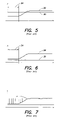
- FIG. 5 illustrates, as an example, a graph of the noise amplitude within the output signal on the line 22 plotted against frequency for an input data signal on the line 14 processed by the circuit 10 of FIG. 4 .
- relatively uniform noise amplitude over all frequencies may be obtained as illustrated by the curve 30 which represents the output signal on the line 22 .
- a noise-shaped output curve 32 is illustrated for the output signal on the line 22 , whose signal to noise ratio may be improved in that there is a reduced noise amplitude in a desired range, for example in an audible range 34 , together with an increased noise amplitude in a higher, non-audible frequency range.
- a noise-shaped output curve 32 is illustrated for the output signal on the line 22 , whose signal to noise ratio may be improved in that there is a reduced noise amplitude in a desired range, for example in an audible range 34 , together with an increased noise amplitude in a higher, non-audible frequency range.
- FIG. 6 illustrates an example of a graph with a curve 36 of the reduced noise level of the output signal on the line 22 for the case of the noise shaper 12 being switched off, as compared to a curve 38 of an increased noise level of the output signal on the line 22 when the noise shaper 12 is switched on.
- Switching off or inactivation of the noise shaper 12 of the prior art circuit 10 of FIG. 4 may lead to undesirable switching noises, also known as clicks.
- the switching noises may be caused by the nonlinearity of an impulse function when a signal or a sequence of data from a data sequence is switched off. This type of switching noise typically is independent of the presence or absence of a DC voltage component, thus the switching noise may also occur when the average signal at the output of the noise shaper 12 on the line 28 is zero.
- the switching noise may typically be due to the low-pass nature of hearing; that is when signal energy is present with a mean value of zero and then is suddenly switched to zero signal energy. This switching process briefly creates frequencies in the overall spectrum, and therefore also in the user frequency band.
- U.S. Pat. No. 5,200,750 discloses a circuit in which an additional input signal is provided to the noise shaper to stabilize the noise structure of the shaper. When the structure is stabilized, the noise shaper can be switched off. However, a relatively complex circuit arrangement and procedure are required in this case.
- U.S. Pat. No. 5,712,874 discloses a circuit arrangement with a low-pass filter for a first integrator of the noise shaper, to automatically stabilize the noise signal or data sequence of the shaper.
- An implementation for a multiple-bit noise shaper may not be possible in this case.
- switching of the low-pass filter may produce a switching noise with an amplitude that is relatively greater than the original switching noise amplitude.
- a noise shaper may be halted on the basis of a prediction of the anticipated specific energy.
- the thesis proposes a method for reducing unwanted in-band transients upon halting of a noise shaper signal.
- a detector may be used as a switching mechanism for controlling the instant at which the quantized signal will be set at zero.
- the switching device for halting the noise shaper may use a model of the noise shaper, on which basis a prediction may be made for the time to switch the noise shaper off.
- Noise that is normally generated during the switching of a noise shaper is reduced by switching the noise shaper to an inactive or off state after the occurrence of one or more predetermined criteria, for example the detection of a predetermined number of data values below a threshold value or equal to a certain value, or of a predetermined number of data values within a threshold region about a value that is constant with respect to the data values.
- a circuit that includes the noise shaper can be configured from a plurality of individual components or in an integrated circuit.
- switching means a general process that involves, depending on the configuration, an active mechanical or electrical switching or a logical switching or deactivation of the noise shaper or of the corresponding process steps of a noise shaper.
- the various predetermined criteria may be independent of each other, or they may be combined or expanded by one or more switching criteria.
- one switching criterion may be that the data values be equal to or below a threshold value.
- a second switching criterion may be that the data values lie within a threshold region about a value that is constant with respect to a sequence of data values, so that a switching process can also occur with a sequence of constant or essentially constant data values. Such a case may occur, for example, when a mono-frequency interfering noise is superimposed on the input data, so that these data values, in the case of absent useful data values that would not be equal to a constant data value, nevertheless remain at a relatively high constant value.
- a sequence of data values and by a predetermined number of data values to be detected may mean that not all of the individual data values within the sequence of data values are subject to the switching criterion each time, so that even in the case of, for example, individual outlying data values the switching criterion can still be fulfilled.
- data values may be used to satisfy the switching criterion that can be detected at various points of the overall switching arrangement.
- input data present at one input of a data processor may be changed by the noise shaper.
- the noise shaper may at times be switched off or inactive.
- the switching off or inactivation, and where for the reduction of the switching noise the switching may be performed after the detection of a predetermined number of data values equal to or below the threshold value.
- data present at an input of a data processor may be changed by the noise shaper.
- the noise shaper may at times be switched off or inactive. To reduce the switching noise the switching may be performed after detecting a predetermined number of data values which lie within a threshold region about a value (e.g., a constant value) relative to a sequence of data values.
- the noise shaper may change input data values of a data sequence provided to a data processor.
- a switching device may be used to inactivate the noise shaper according to one or more predetermined criteria.
- the switching device may have a counter for counting data values equal to or below a threshold value.
- the switching device may switch the noise shaper off after detecting a predetermined number of counted data values equal to or below the threshold value.
- the switching device may have a counter for counting data values within a threshold region about a value (e.g., a constant value) relative to data values adjacent to each other and the switching device may switch off the noise shaper after detecting a predetermined number of counted data values within the threshold region.
- a value e.g., a constant value
- the predetermined number may be variably assigned, for example, the number may be assigned depending on the nature or origin of the data values and/or the fluctuation range of the values of the consecutive data. This may correspond to a noise shaper in which the switching device may variably assign the predetermined number, for example, depending on the nature or origin of the data values and/or depending on the fluctuation range of the values of consecutive data.
- a separate signal for the inactivation may be provided to the noise shaper before the switching or in place of an active switching for a predetermined number of data values. This may correspond to a noise shaper in which the noise shaper has an input for receiving a separate signal for switching off or inactivation during a predetermined duration or number of data values prior to the switching.
- Preprocessed input data values may be provided to the noise shaper prior to the switching or in place of an active switching, where the preprocessing may be performed to gradually reduce the data amplitude over the course of a predetermined number of data values.
- the noise shaper may receive preprocessed data values prior to the switching, where the preprocessed input data values may be provided to gradually reduce the data amplitude over the course of a predetermined number of data values. This may enable an extraction in the event that the data values detected are not equal to a constant data value or may lie above an undesirable value for the switching.
- a reduction of the data values and/or the variables or values generated in the noise shaper may be performed for an additional sequence of data values or an additional period of time.
- a detection of output values may be started and the switching off and/or a resetting of the noise shaper may be performed after the detection of a predetermined number of data values equal to or less than a threshold value at the output of the noise shaper.
- resetting of the noise shaper may be performed to a zero value or to a non-zero value, such as for example 0.5.
- the detected data values may be input data values for the data processor that may be either changed or unchanged by the noise shaper.
- the detected data values may be output data values of the data processor.
- the detected data values may be input data values at the input of the noise shaper. In such a case, the detected data values may be formed from input data values and output data values of the data processor.
- the method and device may be utilized in conjunction with a data processor that may comprise a digital/analog converter or a pulse width modulator.
- the number of detected data values may be reduced in a cascade manner when the noise shaper has not been reset or switched for a particular length of time.
- the energy of a switching noise may become less if the data values output by the noise shaper have already been zero, near zero, or near a constant value for a particular length of time or for a predetermined sequence of data values, before the switching process is carried out.
- an advantageous time for the switching process may be determined. Since the noise shaper outputs data with zero values during intervals of time, such as a pause in the musical titles of a compact disk, and the input data of the layout or the output data of the processing devices also output zero values for a length of time, this has an effect on the energy contained in the pulses that are generated in the entire spectrum during the switching process.
- FIG. 1 is a block diagram of a noise shaper circuit
- FIG. 2 is a flowchart of a method for switching a noise shaper to an inactive or off state
- FIG. 3 is a flowchart of an alternative method for switching a noise shaper to an inactive or off state
- FIG. 4 is a block diagram of a prior art noise shaper circuit
- FIGS. 5–7 are graphs that illustrate various noise signals within the prior art noise shaper circuit of FIG. 4 .
- a circuit 50 may include a data processor 52 and a switching device 54 for switching a noise shaper 56 .
- the components of the circuit 50 of FIG. 1 may be embodied individually or in one or more integrated circuits.
- Input data d in of a signal data sequence on a line 58 may be provided to an adder 60 .
- the output of the adder 60 on a line 62 may be provided to the data processor 52 .
- the input data d in together with a value either added to or subtracted therefrom in the adder 60 , may be processed in the data processor 52 which may comprise, for example, a digital-to-analog converter or a pulse width modulator.
- the data processor 50 may convert a 16-bit signal on the line 62 to a 5-bit signal output on a line 64 .
- the output data d out of the data processor 52 on the line 64 may be provided directly to an output of the circuit 50 or, as illustrated, through one or more additional devices 66 to provide an output on a line 68 .
- the additional processing device 66 for example may be a low-pass filter that may be used to determine an amplitude of a switching noise to test the effects of the overall circuit layout on switching noises.
- the output data d out on the line 64 may be provided to a subtractor 70 , which subtracts the data 60 on the line 62 from the output data d out on the line 64 .
- the output d sub of the subtractor 70 on a line 72 may input to the noise shaper 56 .
- the noise shaper 56 may comprise a high-pass filter with an arrangement of delay elements.
- the output signal of the noise shaper 56 may be provided on a line 74 to the adder 60 where it may be added to the input data d in on the line 58 .
- the switching device 54 may comprise a counter and a memory for saving the count values and certain preset variables.
- the switching device 54 may generate a switch signal on a line 76 for resetting the noise shaper 56 and/or for switching the noise shaper 56 to an inactive or off state when, for example, no input data d in for processing have been entered into the circuit 50 or are being processed therein.
- the noise shaper input data d sub on the line 72 may also be provided to the switching device 54 for processing thereby.
- resetting of the noise shaper 56 in particular the high-pass filter therein, may occur in particular by resetting the memory in the switching device 54 at the same time.
- An input of the switching device 54 may be connected by the line 64 to a data relaying point of the circuit 50 .
- the data relaying point may depend on which of the data within the circuits are to be used as the basis for a switching criterion.
- the data utilized as the basis for the switching criterion may be the output data d out of the data processor on the line 64 .
- a number of variables n, m, s, t may have predetermined values assigned to them. These variables may be stored for example in the memory of the switching device 54 .
- a variable s is assigned the value of the data point currently being detected or taken into account, for example, d in , d out and/or d sub .
- a check may be performed whether the value of the data variable s is less than or equal to the predetermined value of the threshold variable t.
- the threshold value t can be chosen such that, during the allocation of the variables in the step 80 , the threshold value t may be a constant or a variable, depending for example on the operating circumstances. If the value of the data variable s is less than or equal to the threshold value t, a running index m originally set at zero in the step 80 may be incremented by one in a step 86 . In a following comparison step 88 , a check may be made whether the value of the running index m, is greater than or equal to a predetermined number n of the data being detected. Thus, the running index m corresponds to a count value of the counter.
- the running index m is less than the predetermined number n, there may be a return to the input step 82 to enter a next value of the data being detected (e.g., d in , d out , d sub ). If, instead, the running index m is greater than or equal to the predetermined number n, the noise shaper may be switched off, reset, or placed in an inactive state in a step 90 . This may occur, for example, by generating the switch signal on the line 76 ( FIG. 1 ). The method then returns to the input step 82 . If it is determined in the comparison step 84 that the value of the data variable s is greater than the threshold value t, the running index m may be set at zero, i.e., the counter may be reset in a step 92 .
- the method thus checks to see whether a sequence of a number of consecutive data points (d in , d out , d sub ) is less than or equal to the threshold value t. If so, the noise shaper 56 ( FIG. 1 ) may be inactivated or switched off. Increasingly larger predetermined numbers n may be able to achieve an increasingly greater reduction of the switching noise upon inactivation or resetting of the noise shaper 56 . Therefore, depending on the required or desired reduction in the switching noise, the predetermined number n may be assigned according to the application purpose and need. In particular, a variable assigning of the predetermined number n may be possible, so as to be able to adapt to changed operating conditions.
- the threshold value t can either be a constant or be variably adapted, the latter in order to be able to adapt to changed operating conditions or immediate requirements.
- the threshold value t may also be set to zero, and the determination of a suitable threshold value will depend on the conditions of the moment.
- a sequence of consecutive data values may be considered as to whether they contain one or more outlying data values that individually exceed the threshold value t.
- a certain number of individual outlying data values may be allowed that can exceed the threshold value t within a sequence of data before reactivation occurs.
- the switching of the noise shaper 56 ( FIG. 1 ) to the inactive or off state may occur when a sequence of n number of data points (d in , d out , d sub ) corresponds to a constant value or lies about a constant value within a threshold region.
- the threshold value t accordingly, may indicate the limit for the threshold region.
- a first step 100 an allocation of the variables n, m, t, s, so may be performed.
- the detected data (d in , d out , d sub ) may be entered and assigned to the data variable s.
- a prior value of the data variable s may be saved in a data variable s o .
- a difference may be formed between the values of the data variables s and s o and the absolute magnitude of the difference may be compared to the threshold value t. If the difference is less than the threshold value t, the running index m may be incremented by one in step 106 .
- a check may be performed as to whether the running index m is less than or equal to the predetermined number n.
- step 104 determines that the difference is equal to or greater than the threshold value t, the running index m and the data variables s and so may be reset in a step 112 .
- certain ones of the data values may be masked.
- the masking may be used, for example, when constant data values are present or when data values may be too high for inactivation of the noise shaper 56 .
- These values may be reduced gradually by a number of reductions, o, of consecutive data points (d in , d out , d sub ) to a value that enables inactivation of the noise shaper with sufficiently low residual switching noise.
- an auxiliary data variable a may be increased by the current value of the data variable s.
- a sequence of additional data processing steps may be performed prior to step 110 of resetting the noise shaper 56 .
- an additional reduction variable b as a reduction factor, may equal a value of one minus the value of the auxiliary data variable a divided by the reduction number o of masking steps minus a number of masking steps performed j.
- the reduction variable b may be multiplied in a step 116 with the current data value or with another value being masked.
- a masking running index for the number of masking steps performed j may be incremented by one in step 118 prior to step 116 .
- the masking running index j may be checked in step 120 to determine if it is less than or equal to the reduction number o, i.e., the duration of the masking. If so, there is a return to the input step 102 . If not, then the noise shaper 56 is inactivated in step 110 . If in step 104 it is determined that the difference is greater than or equal to the threshold value t, there may also be a resetting of the auxiliary data variable a and the masking running index j in step 112 .
- the circuit illustrated in FIG. 1 and the methods illustrated in the flowcharts FIGS. 2 and 3 may continuously count the number of contiguous zeroes at the output of the noise shaper 56 . If a sampled value or data value is zero, the counter may be reset and may start counting again. A particular number n of zeroes detected per unit at the output the switch signal 76 provided to the noise shaper 56 thereupon may erase all the delay elements of the noise shaper at the same time. Since the input data d in and the output data d out at this time may already be zero, the noise shaper 56 may remain empty until a value of the input data d in not equal to zero may again be provided by the data processor 52 .
- the noise shaper 56 may be reset once the data input has been constant for a particular number of data values.
- the switching criterion may be whether the output data values d out may be equal to zero or less than a threshold value t. It may be advantageous to switch the circuit 50 with the noise shaper 56 for example by using a constant input signal in the noise shaper 56 for a particular length of time or number of consecutive data values.
- the predetermined number of data used as the switching criterion can be adjusted variably.
- the noise shaper may be switched off or inactivated with reduced switching noise. This may be accomplished without a specific turn-off command, which would analyze the input signal on the line 72 to the noise shaper 56 and then may activate the detection of zero values at very low signal levels.
- the zero detection itself may switch the noise shaper 56 on and off, when a particular number of zero values or corresponding values below a threshold value may be detected at the output.
- a particular number of zeroes may be assigned to a particular signal amplitude, which helps to achieve a relatively small input signal after a particular number of detected zero values.
- the number of zeroes needed for the resetting can be cascaded. For example, when starting with 64 zeroes, if the noise shaper has not been reset for a certain length of time, the number can be reduced to the detection of 32 zeroes as the switching criterion. If, after another particular time period 32 zeroes are not detected, then the detection may be converted to 16 zeroes, and so forth.
Landscapes
- Engineering & Computer Science (AREA)
- Theoretical Computer Science (AREA)
- Compression, Expansion, Code Conversion, And Decoders (AREA)
- Dc-Dc Converters (AREA)
- Electronic Switches (AREA)
Applications Claiming Priority (2)
| Application Number | Priority Date | Filing Date | Title |
|---|---|---|---|
| DE102004039725.2 | 2004-08-11 | ||
| DE102004039725A DE102004039725A1 (de) | 2004-08-11 | 2004-08-11 | Rauschformerschaltung und Verfahren zum Reduzieren eines Schaltgeräusches |
Publications (2)
| Publication Number | Publication Date |
|---|---|
| US20060044166A1 US20060044166A1 (en) | 2006-03-02 |
| US7233271B2 true US7233271B2 (en) | 2007-06-19 |
Family
ID=35169849
Family Applications (1)
| Application Number | Title | Priority Date | Filing Date |
|---|---|---|---|
| US11/202,636 Expired - Fee Related US7233271B2 (en) | 2004-08-11 | 2005-08-11 | Noise shaper circuit and method for reducing switching noise |
Country Status (4)
| Country | Link |
|---|---|
| US (1) | US7233271B2 (de) |
| EP (1) | EP1626503A3 (de) |
| JP (1) | JP2006054855A (de) |
| DE (1) | DE102004039725A1 (de) |
Families Citing this family (3)
| Publication number | Priority date | Publication date | Assignee | Title |
|---|---|---|---|---|
| US8243916B2 (en) * | 2007-01-15 | 2012-08-14 | Lantiq Deutschland Gmbh | CODEC circuit for POTS system |
| US8390494B2 (en) * | 2010-01-15 | 2013-03-05 | Asahi Kasei Microdevices Corporation | Second order noise coupling with zero optimization modulator and method |
| US11804814B1 (en) * | 2022-04-13 | 2023-10-31 | Stmicroelectronics S.R.L. | Noise shaper fader |
Citations (14)
| Publication number | Priority date | Publication date | Assignee | Title |
|---|---|---|---|---|
| US3918042A (en) * | 1974-04-29 | 1975-11-04 | Motorola Inc | Delta modulator having increased dynamic range |
| US5157216A (en) * | 1990-01-16 | 1992-10-20 | The Board Of Trustees Of The Leland Stanford Junior University | Musical synthesizer system and method using pulsed noise for simulating the noise component of musical tones |
| US5200750A (en) | 1990-11-22 | 1993-04-06 | Yamaha Corporation | Digital-to-analog converter with noise-free sigma-delta modulation |
| US5235334A (en) | 1992-03-30 | 1993-08-10 | Motorola, Inc. | Digital-to-analog converter with a linear interpolator |
| US5682162A (en) | 1994-12-27 | 1997-10-28 | Burr-Brown Corporation | Oversampling digital-to-analog converter with auto-muting feature |
| US5712874A (en) | 1993-12-07 | 1998-01-27 | Nec Corpoation | Noise shaper capable of generating a predetermined output pattern in no-signal condition |
| US5890059A (en) * | 1996-10-21 | 1999-03-30 | Delco Electronics Corporation | Impulse noise blanking apparatus |
| US5999347A (en) | 1993-06-29 | 1999-12-07 | Sony Corporation | Method and apparatus for higher resolution audio signal transmitting |
| US6137429A (en) * | 1999-03-08 | 2000-10-24 | Motorola, Inc. | Circuit and method for attenuating noise in a data converter |
| US6208279B1 (en) * | 1998-08-17 | 2001-03-27 | Linear Technology Dorporation | Single-cycle oversampling analog-to-digital converter |
| US6369731B1 (en) | 1999-12-09 | 2002-04-09 | Nippon Precision Circuits Inc. | Delta sigma D/A converter |
| JP2003017945A (ja) | 2001-07-04 | 2003-01-17 | Sharp Corp | ミューティング回路 |
| US20040017854A1 (en) * | 2002-07-26 | 2004-01-29 | Hansen Thomas H. | Method and circuit for stop of signals quantized using noise-shaping |
| US6778118B2 (en) * | 2002-05-03 | 2004-08-17 | Thomson Licensing S.A. | Thermometer code digital to audio converter |
Family Cites Families (3)
| Publication number | Priority date | Publication date | Assignee | Title |
|---|---|---|---|---|
| JPH07118647B2 (ja) * | 1992-07-20 | 1995-12-18 | 日本プレシジョン・サーキッツ株式会社 | オーバーサンプリング型d/aコンバータ制御回路 |
| JP3857028B2 (ja) * | 2000-09-05 | 2006-12-13 | 株式会社リコー | デジタル・アナログ変換回路及びそれを用いた再生装置 |
| GB0200027D0 (en) * | 2002-01-02 | 2002-02-13 | Bae Systems Plc | Improvements relating to operation of a current controller |
-
2004
- 2004-08-11 DE DE102004039725A patent/DE102004039725A1/de not_active Withdrawn
-
2005
- 2005-05-13 EP EP05010465A patent/EP1626503A3/de not_active Withdrawn
- 2005-06-29 JP JP2005189775A patent/JP2006054855A/ja active Pending
- 2005-08-11 US US11/202,636 patent/US7233271B2/en not_active Expired - Fee Related
Patent Citations (14)
| Publication number | Priority date | Publication date | Assignee | Title |
|---|---|---|---|---|
| US3918042A (en) * | 1974-04-29 | 1975-11-04 | Motorola Inc | Delta modulator having increased dynamic range |
| US5157216A (en) * | 1990-01-16 | 1992-10-20 | The Board Of Trustees Of The Leland Stanford Junior University | Musical synthesizer system and method using pulsed noise for simulating the noise component of musical tones |
| US5200750A (en) | 1990-11-22 | 1993-04-06 | Yamaha Corporation | Digital-to-analog converter with noise-free sigma-delta modulation |
| US5235334A (en) | 1992-03-30 | 1993-08-10 | Motorola, Inc. | Digital-to-analog converter with a linear interpolator |
| US5999347A (en) | 1993-06-29 | 1999-12-07 | Sony Corporation | Method and apparatus for higher resolution audio signal transmitting |
| US5712874A (en) | 1993-12-07 | 1998-01-27 | Nec Corpoation | Noise shaper capable of generating a predetermined output pattern in no-signal condition |
| US5682162A (en) | 1994-12-27 | 1997-10-28 | Burr-Brown Corporation | Oversampling digital-to-analog converter with auto-muting feature |
| US5890059A (en) * | 1996-10-21 | 1999-03-30 | Delco Electronics Corporation | Impulse noise blanking apparatus |
| US6208279B1 (en) * | 1998-08-17 | 2001-03-27 | Linear Technology Dorporation | Single-cycle oversampling analog-to-digital converter |
| US6137429A (en) * | 1999-03-08 | 2000-10-24 | Motorola, Inc. | Circuit and method for attenuating noise in a data converter |
| US6369731B1 (en) | 1999-12-09 | 2002-04-09 | Nippon Precision Circuits Inc. | Delta sigma D/A converter |
| JP2003017945A (ja) | 2001-07-04 | 2003-01-17 | Sharp Corp | ミューティング回路 |
| US6778118B2 (en) * | 2002-05-03 | 2004-08-17 | Thomson Licensing S.A. | Thermometer code digital to audio converter |
| US20040017854A1 (en) * | 2002-07-26 | 2004-01-29 | Hansen Thomas H. | Method and circuit for stop of signals quantized using noise-shaping |
Non-Patent Citations (1)
| Title |
|---|
| Thomas H. Hansen, "Muting of Noise-Shaper Quantized Signals," pp. 77-94, May 6, 2003. |
Also Published As
| Publication number | Publication date |
|---|---|
| EP1626503A3 (de) | 2006-08-30 |
| DE102004039725A1 (de) | 2006-02-23 |
| US20060044166A1 (en) | 2006-03-02 |
| EP1626503A2 (de) | 2006-02-15 |
| JP2006054855A (ja) | 2006-02-23 |
Similar Documents
| Publication | Publication Date | Title |
|---|---|---|
| US6453282B1 (en) | Method and device for detecting a transient in a discrete-time audiosignal | |
| US6353404B1 (en) | D/A conversion apparatus and D/A conversion method | |
| US7535859B2 (en) | Voice activity detection with adaptive noise floor tracking | |
| KR20060004695A (ko) | 오디오 신호의 대역을 확장하기 위한 방법 및 장치 | |
| CA2665153A1 (en) | Audio dynamics processing using a reset | |
| JP2002509620A (ja) | 音声信号障害を低減するための方法 | |
| KR930007298B1 (ko) | 펄스형 간섭 검출장치 | |
| US8611572B2 (en) | Device and method for controlling the step size of an adaptive filter | |
| US20060044166A1 (en) | Noise shaper circuit and method for reducing switching noise | |
| KR0179936B1 (ko) | 디지탈 오디오 프로세서의 노이즈 게이트 장치 | |
| JP3847222B2 (ja) | ノイズスパイクを除去するための方法と装置 | |
| US8786481B1 (en) | Method and apparatus for event detection and adaptive system power reduction using analog compression engine | |
| KR100427467B1 (ko) | 전력 변환 장치 | |
| WO1996021975A1 (en) | Method and apparatus for determining a masked threshold | |
| CN112514263B (zh) | 模数转换器和操作模数转换器的方法 | |
| JP4885835B2 (ja) | Δς変調装置、δς変調の停止方法、プログラム、および、記録媒体 | |
| KR101993003B1 (ko) | 잡음 제거 장치 및 방법 | |
| JP3302574B2 (ja) | デルタシグマ変調回路 | |
| JPS646574B2 (de) | ||
| KR970002195B1 (ko) | 디지탈기기의 음소거장치 및 음소거 제어방법 | |
| EP0419127A2 (de) | Geräuschunterdrückungssystem | |
| CA2052600C (en) | Adaptive bandwidth moving average filter | |
| US9807284B2 (en) | Method and device for noise suppression in a data processing arrangement | |
| JP3713289B2 (ja) | デジタル信号処理方式 | |
| JPH09246983A (ja) | ディジタル信号処理装置 |
Legal Events
| Date | Code | Title | Description |
|---|---|---|---|
| AS | Assignment |
Owner name: MICRONAS GMBH, GERMANY Free format text: ASSIGNMENT OF ASSIGNORS INTEREST;ASSIGNORS:PFISTER, FLORIAN;LUECKING, DIETER;VIERTHALER, MATTHIAS;AND OTHERS;REEL/FRAME:016925/0197;SIGNING DATES FROM 20050916 TO 20051011 |
|
| STCF | Information on status: patent grant |
Free format text: PATENTED CASE |
|
| FEPP | Fee payment procedure |
Free format text: PAYER NUMBER DE-ASSIGNED (ORIGINAL EVENT CODE: RMPN); ENTITY STATUS OF PATENT OWNER: LARGE ENTITY Free format text: PAYOR NUMBER ASSIGNED (ORIGINAL EVENT CODE: ASPN); ENTITY STATUS OF PATENT OWNER: LARGE ENTITY |
|
| AS | Assignment |
Owner name: TRIDENT MICROSYSTEMS (FAR EAST) LTD.,CAYMAN ISLAND Free format text: ASSIGNMENT OF ASSIGNORS INTEREST;ASSIGNOR:MICRONAS GMBH;REEL/FRAME:024456/0453 Effective date: 20100408 Owner name: TRIDENT MICROSYSTEMS (FAR EAST) LTD., CAYMAN ISLAN Free format text: ASSIGNMENT OF ASSIGNORS INTEREST;ASSIGNOR:MICRONAS GMBH;REEL/FRAME:024456/0453 Effective date: 20100408 |
|
| FPAY | Fee payment |
Year of fee payment: 4 |
|
| AS | Assignment |
Owner name: ENTROPIC COMMUNICATIONS, INC., CALIFORNIA Free format text: ASSIGNMENT OF ASSIGNORS INTEREST;ASSIGNORS:TRIDENT MICROSYSTEMS, INC.;TRIDENT MICROSYSTEMS (FAR EAST) LTD.;REEL/FRAME:028153/0530 Effective date: 20120411 |
|
| FPAY | Fee payment |
Year of fee payment: 8 |
|
| AS | Assignment |
Owner name: ENTROPIC COMMUNICATIONS, INC., CALIFORNIA Free format text: MERGER AND CHANGE OF NAME;ASSIGNORS:EXCALIBUR ACQUISITION CORPORATION;ENTROPIC COMMUNICATIONS, INC.;ENTROPIC COMMUNICATIONS, INC.;REEL/FRAME:035706/0267 Effective date: 20150430 |
|
| AS | Assignment |
Owner name: ENTROPIC COMMUNICATIONS, LLC, CALIFORNIA Free format text: MERGER AND CHANGE OF NAME;ASSIGNORS:ENTROPIC COMMUNICATIONS, INC.;EXCALIBUR SUBSIDIARY, LLC;ENTROPIC COMMUNICATIONS, LLC;REEL/FRAME:035717/0628 Effective date: 20150430 |
|
| AS | Assignment |
Owner name: JPMORGAN CHASE BANK, N.A., AS COLLATERAL AGENT, IL Free format text: SECURITY AGREEMENT;ASSIGNORS:MAXLINEAR, INC.;ENTROPIC COMMUNICATIONS, LLC (F/K/A ENTROPIC COMMUNICATIONS, INC.);EXAR CORPORATION;REEL/FRAME:042453/0001 Effective date: 20170512 Owner name: JPMORGAN CHASE BANK, N.A., AS COLLATERAL AGENT, ILLINOIS Free format text: SECURITY AGREEMENT;ASSIGNORS:MAXLINEAR, INC.;ENTROPIC COMMUNICATIONS, LLC (F/K/A ENTROPIC COMMUNICATIONS, INC.);EXAR CORPORATION;REEL/FRAME:042453/0001 Effective date: 20170512 |
|
| FEPP | Fee payment procedure |
Free format text: MAINTENANCE FEE REMINDER MAILED (ORIGINAL EVENT CODE: REM.); ENTITY STATUS OF PATENT OWNER: LARGE ENTITY |
|
| LAPS | Lapse for failure to pay maintenance fees |
Free format text: PATENT EXPIRED FOR FAILURE TO PAY MAINTENANCE FEES (ORIGINAL EVENT CODE: EXP.); ENTITY STATUS OF PATENT OWNER: LARGE ENTITY |
|
| STCH | Information on status: patent discontinuation |
Free format text: PATENT EXPIRED DUE TO NONPAYMENT OF MAINTENANCE FEES UNDER 37 CFR 1.362 |
|
| FP | Lapsed due to failure to pay maintenance fee |
Effective date: 20190619 |
|
| AS | Assignment |
Owner name: MUFG UNION BANK, N.A., CALIFORNIA Free format text: SUCCESSION OF AGENCY (REEL 042453 / FRAME 0001);ASSIGNOR:JPMORGAN CHASE BANK, N.A.;REEL/FRAME:053115/0842 Effective date: 20200701 |
|
| AS | Assignment |
Owner name: MAXLINEAR, INC., CALIFORNIA Free format text: RELEASE BY SECURED PARTY;ASSIGNOR:MUFG UNION BANK, N.A.;REEL/FRAME:056656/0204 Effective date: 20210623 Owner name: EXAR CORPORATION, CALIFORNIA Free format text: RELEASE BY SECURED PARTY;ASSIGNOR:MUFG UNION BANK, N.A.;REEL/FRAME:056656/0204 Effective date: 20210623 Owner name: MAXLINEAR COMMUNICATIONS LLC, CALIFORNIA Free format text: RELEASE BY SECURED PARTY;ASSIGNOR:MUFG UNION BANK, N.A.;REEL/FRAME:056656/0204 Effective date: 20210623 Owner name: MAXLINEAR, INC., CALIFORNIA Free format text: RELEASE OF SECURITY INTEREST;ASSIGNOR:MUFG UNION BANK, N.A.;REEL/FRAME:056656/0204 Effective date: 20210623 Owner name: EXAR CORPORATION, CALIFORNIA Free format text: RELEASE OF SECURITY INTEREST;ASSIGNOR:MUFG UNION BANK, N.A.;REEL/FRAME:056656/0204 Effective date: 20210623 Owner name: MAXLINEAR COMMUNICATIONS LLC, CALIFORNIA Free format text: RELEASE OF SECURITY INTEREST;ASSIGNOR:MUFG UNION BANK, N.A.;REEL/FRAME:056656/0204 Effective date: 20210623 |