US7139849B2 - Semiconductor integrated circuit device - Google Patents
Semiconductor integrated circuit device Download PDFInfo
- Publication number
- US7139849B2 US7139849B2 US10/624,598 US62459803A US7139849B2 US 7139849 B2 US7139849 B2 US 7139849B2 US 62459803 A US62459803 A US 62459803A US 7139849 B2 US7139849 B2 US 7139849B2
- Authority
- US
- United States
- Prior art keywords
- processing unit
- memory
- bus
- integrated circuit
- semiconductor integrated
- Prior art date
- Legal status (The legal status is an assumption and is not a legal conclusion. Google has not performed a legal analysis and makes no representation as to the accuracy of the status listed.)
- Expired - Fee Related, expires
Links
Images


Classifications
-
- G—PHYSICS
- G06—COMPUTING; CALCULATING OR COUNTING
- G06F—ELECTRIC DIGITAL DATA PROCESSING
- G06F12/00—Accessing, addressing or allocating within memory systems or architectures
-
- G—PHYSICS
- G06—COMPUTING; CALCULATING OR COUNTING
- G06F—ELECTRIC DIGITAL DATA PROCESSING
- G06F12/00—Accessing, addressing or allocating within memory systems or architectures
- G06F12/02—Addressing or allocation; Relocation
- G06F12/06—Addressing a physical block of locations, e.g. base addressing, module addressing, memory dedication
- G06F12/0646—Configuration or reconfiguration
- G06F12/0692—Multiconfiguration, e.g. local and global addressing
-
- G—PHYSICS
- G06—COMPUTING; CALCULATING OR COUNTING
- G06F—ELECTRIC DIGITAL DATA PROCESSING
- G06F15/00—Digital computers in general; Data processing equipment in general
- G06F15/76—Architectures of general purpose stored program computers
- G06F15/78—Architectures of general purpose stored program computers comprising a single central processing unit
- G06F15/7839—Architectures of general purpose stored program computers comprising a single central processing unit with memory
- G06F15/7842—Architectures of general purpose stored program computers comprising a single central processing unit with memory on one IC chip (single chip microcontrollers)
- G06F15/7857—Architectures of general purpose stored program computers comprising a single central processing unit with memory on one IC chip (single chip microcontrollers) using interleaved memory
Definitions
- the present invention relates to semiconductor integrated circuit devices that include a plurality of internal memories and a plurality of processing units for data processing, and that operate while being connected to an external processing unit.
- JP H10-27131A discloses a shared memory device performing conflict control for DMA transfer requests from a plurality of communication controllers, wherein even while one memory bank is being used, access to other memory banks is possible, and thus the frequency that the communications controllers are caused to wait by shared memory access is reduced.
- JP H10-260952A discloses a technology for flexibly connecting the processors and the memory banks in a multiprocessor system LSI with an integrated multibank memory.
- JP 2000-99391A discloses a printer device, in which memory banks can be accessed simultaneously by mediating access to the memory banks of a memory individually for each memory bank.
- JP 2001-43180A discloses a microprocessor in which a plurality of resources share a single memory, and no-wait access is possible in parallel.
- a semiconductor integrated circuit in accordance with the present invention which operates while being connected to an external processing unit, includes a plurality of internal memories, a first processing unit for data processing and a second processing unit for data processing, and a memory configuration controller for controlling the assignment of the plurality of internal memories to the first processing unit, the second processing unit and the external processing unit in accordance with an application.
- the plurality of internal memories can be allocated to the first processing unit, the second processing unit and the external processing unit respectively, or the plurality of internal memories all can be occupied exclusively by the first or the second processing unit. Furthermore, it is also possible that the plurality of internal memories are all occupied by the external processing unit. In this last example, the semiconductor integrated circuit device operates merely as a memory device for the external processing unit.
- FIG. 1 is a block diagram showing an example of the internal configuration of a semiconductor integrated circuit device according to the present invention, as well as its external connections.
- FIG. 2 is a block diagram showing a more detailed configuration example of the memory configuration controller in FIG. 1 .
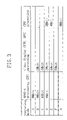
- FIG. 3 shows an example of the memory allocation for each operation mode, in accordance with the application of the semiconductor integrated circuit in FIG. 1 .
- FIG. 4A shows an example of a first register for specifying the intended use of the memories in the semiconductor integrated circuit device in FIG. 1
- FIG. 4B illustrates the meaning of the least significant two bits in that register.
- FIG. 5A shows an example of a second register for specifying the storage capacity of the memories in the semiconductor integrated circuit device in FIG. 1
- FIG. 5B illustrates the meaning of the least significant bit in that register
- FIG. 5C illustrates the meaning of the most significant two bits in that register.
- FIG. 6A shows an example of specifying absolute addresses for the memory assigned to the external CPU in the semiconductor integrated circuit device of FIG. 1
- FIG. 6B shows an example of specifying relative addresses for the memory assigned to the external CPU.
- FIG. 7 is a block diagram showing an example of the configuration of a portable communication terminal using the semiconductor integrated circuit device in FIG. 1 as an image processor.
- FIG. 1 shows an example of the internal configuration of a semiconductor integrated circuit device according to the present invention, as well as its external connections.
- the semiconductor integrated circuit device 10 in FIG. 1 which is for image processing, operates while being connected to a CPU 11 , which is an external processing unit, a camera 12 for image input, a liquid crystal display (LCD) 13 for image display, and an external memory 14 made of an SDRAM.
- the maximum storage capacity of the external memory 14 is for example 256 Mbit (megabit).
- the semiconductor integrated circuit device 10 includes a plurality of internal memories 20 to 23 made of SRAMs 0 to 3, a main processor (MP) 24 , a video interface (VIF) 25 , a graphics processor (GFX) 26 , a host interface (HIF) 27 , and an asynchronous serial interface (UART) 28 .
- the main processor 24 is a first processing unit for image data processing and has a codec (encode/decode) function in accordance with MPEG-4.
- the video interface 25 and the graphics processor 26 constitute a second processing unit for image data processing, controlling the video display processing.
- the storage capacity of the internal memories 20 to 23 is, for example, 2 Mbit or 4 Mbit each.
- the video interface 25 is connected to the camera 12 and the liquid crystal display 13 , whereas the host interface 27 and the asynchronous serial interface 28 are connected to the CPU 11 .
- the semiconductor integrated circuit device 10 of FIG. 1 is further provided with a memory controller 30 including a memory configuration controller 31 .
- the memory configuration controller 31 controls the allocation of memory for the main processor 24 , the video interface 25 , the graphics processor 26 , and the CPU 11 , in accordance with the application.
- a memory is assigned to the main processor 24 , and used by it as a work region.
- a memory is assigned to the video interface 25 and the graphics processor 26 , and used by them as a frame region, which is commonly called “frame memory.”
- a memory is assigned to the CPU 11 , and used by it as a CPU region.
- the memory controller 30 further includes a work region memory interface (WMIF) 32 serving as a first memory interface, a frame region memory interface (FMIF) 33 serving as a second memory interface, and a CPU region memory interface (CPUIF) 34 serving as a third memory interface.
- WMIF work region memory interface
- FMIF frame region memory interface
- CPUF CPU region memory interface
- the semiconductor integrated circuit device 10 in FIG. 1 is provided with a WM bus (first data bus) 40 , an FM bus (second data bus) 41 , and a CPU bus (third data bus) 42 dedicated to the CPU 11 .
- the WMIF 32 is interposed between the work region assigned to the main processor 24 and the WM bus 40 , and mediates and controls DMA data transfer requests.
- the FMIF 33 is interposed between the frame region assigned to the video interface 25 and the graphics processor 26 on the one hand and the FM bus 41 on the other hand, and mediates and controls DMA data transfer requests.
- the CPUIF 34 is interposed between the CPU region and the CPU bus 42 , and is an interface controlling data transfer.
- the memory assigned to the work region can be accessed via the WMIF 32
- the memory assigned to the frame region can be accessed via the FMIF 33
- the memory assigned to the CPU region can be accessed via the CPUIF 34 .
- a host bus 43 is provided between the graphics processor 26 and the host interface 27 .
- the main processor 24 includes a local bus 44 that is connected to the host interface 27 .
- the main processor 24 can be connected via an MP bus selector 50 to either the WM bus 40 or the FM bus 41 , and is provided over a local bus 44 with a plurality of local memories (DM 1 , DM 2 and DM 3 ) 51 to 53 and a plurality of hardware engines (ENG) 54 .
- the hardware engines 54 are partial processing cores for encoding/encoding MPEG image data.
- the video interface 25 can be connected via a VIF bus selector 55 to either the WM bus 40 or the FM bus 41 .
- the graphics processor 26 can be connected only to the FM bus 41 and not to the WM bus 40 .
- the host interface 27 can be connected via an HIF bus selector 60 to either the WM bus 40 or the FM bus 41 .
- the host interface 27 can be connected via the CPU bus 42 and the CPU IF bus selector 61 to either the CPU IF 34 or the FM bus 41 .
- the asynchronous serial interface 28 can be connected via the UART bus selector 62 to either the WM bus 40 or the FM bus 41 .
- the main processor 24 can instruct a DMA data transfer between the local memories 51 to 53 and the work region via the MP bus selector 50 , the WM bus 40 and the WMIF 32 , and it can instruct a DMA data transfer between the local memories 51 to 53 and the frame region via the MP bus selector 50 , the FM bus 41 and the FMIF 33 . Furthermore, the main processor 24 can instruct a DMA data transfer between the a host memory within the host interface 27 and the work region via the HIF bus selector 60 , the WM bus 40 and the WMIF 32 , and it can instruct a DMA data transfer between the a host memory within the host interface 27 and the frame region via the HIF bus selector 60 , the FM bus 41 and the FMIF 33 .
- the main processor 24 can instruct a DMA data transfer between the a FIFO memory within the asynchronous serial interface 28 and the work region via the UART bus selector 62 , the WM bus 40 and the WMIF 32 , and it can instruct a DMA data transfer between the a FIFO memory within the asynchronous serial interface 28 and the frame region via the UART bus selector 62 , the FM bus 41 and the FMIF 33 .
- the DMA data transfer between the local memories 51 to 53 and the work region and the DMA data transfer with the host memory within the host interface 27 or the FIFO memory within the asynchronous serial interface 28 can be carried out in parallel.
- the DMA data transfer between the local memories 51 to 53 and the frame region and the DMA data transfer with the host memory within the host interface 27 or the FIFO memory within the asynchronous serial interface 28 also can be carried out in parallel.
- the main processor 24 can instruct a DMA data transfer between an internal memory of the video interface 25 and the work region via the VIF bus selector 55 , the WM bus 40 and the WMIF 32 , and it can instruct a DMA data transfer between the internal memory of the video interface 25 and the frame region via the VIF bus selector 55 , the FM bus 41 and the FMIF 33 . Furthermore, the main processor 24 can instruct a DMA data transfer between the internal memory of the graphics processor 26 and the frame region via the FM bus 41 and the FMIF 33 .
- the DMA data transfer between the local memories 51 to 53 of the main processor 24 and the work region and the DMA data transfer between the internal memories of the video interface 25 and the graphics processor 26 and the frame region can be carried out in parallel.
- the DMA data transfer between the local memories 51 to 53 of the main processor 24 and the frame region and the DMA data transfer between the internal memories of the video interface 25 and the graphics processor 26 and the work region also can be carried out in parallel. It is also possible to proceed with the data processing using the local memories 51 to 53 , while the main processor 24 carries out a DMA data transfer for the video interface 25 for example.
- the CPU 11 is provided with three memory access routes for parallel data. First, there is access via the host interface 27 , with which writing from the CPU 11 into the host memory provided within the host interface 27 is performed. In response to this, the main processor 24 instructs a DMA data transfer between the host memory and the work region or the frame region. Thus, the CPU 11 can achieve the writing of graphics data into a portion of the frame region, for example. Second, there is a route for the case that the CPU 11 accesses the CPU region without passing through the host memory, and this route passes from the CPU 11 through the host interface 27 , the CPU bus 42 , the CPUIF bus selector 61 , and the CPUIF 34 to the CPU region.
- FIG. 2 shows a more detailed configuration example of the memory configuration controller 31 in FIG. 1 .
- the memory configuration controller 31 has a setting portion 70 , and this setting portion 70 includes a first register 71 for specifying the intended use of the memories, and a second register 72 for specifying the storage capacity of the memories.
- a read/write controller 73 directs access signals from the WMIF 32 , the FMIF 33 and the CPUIF 34 to the individual memories.
- the first and the second registers 71 and 72 can be set as desired by the main processor 24 and the CPU 11 .
- FIG. 3 shows an example of the memory allocation for each operation mode, in accordance with the application of the semiconductor integrated circuit device 10 in FIG. 1 .
- each of the four internal memories 20 to 23 is assumed to have a storage capacity of 2 Mbit. This means that the total storage capacity of the internal memories 20 to 23 is 8 Mbit.
- the memory configuration controller 31 plays the important roll of effectively putting to use the these limited memory resources.
- an operating mode A all of the internal memories 20 to 23 are occupied by the main processor 24 .
- 6 Mbit of the total capacity of the internal memories 20 to 23 are allocated to the main processor 24
- 2 Mbit are allocated to the video interface 25 and the graphics processor 26 .
- the operating mode C 4 Mbit of the total capacity of the internal memories 20 to 23 are allocated to the main processor 24 , and 4 Mbit are allocated to the video interface 25 and the graphics processor 26 .
- the operating mode D 4 Mbit of the total capacity of the internal memories 20 to 23 is allocated to the main processor 24 , 2 Mbit are allocated to the video interface 25 and the graphics processor 26 , and 2 Mbit are allocated to the CPU 11 .
- the operating mode E 4 Mbit of the total capacity of the internal memories 20 to 23 are allocated to the video interface 25 and the graphics processor 26 , and 4 Mbit are allocated to the CPU 11 .
- the operating mode F all of the internal memories 20 to 23 are occupied by the video interface 25 and the graphics processor 26 .
- FIG. 4A shows an example of a first register 71 with a 10-bit configuration
- FIG. 4B illustrates the meaning of the least significant two bits in that register. If the bits 1 and 0 of the first register 71 allocated to the SRAM 0 , which is one of the internal memories 20 to 23 , are “00,” then the SRAM 0 is used as a work region, if they are “01,” then the SRAM 0 is used as a frame region, if they are “10,” then the SRAM 0 is used as a CPU region.
- the bits 1 and 0 of the first register 71 should be set to “11.” In this case, the supply of power to the SRAM 0 is stopped, and it can be ensured that no addresses are allocated to that SRAM 0 .
- the bits 3 and 2 of the first register 71 specify the intended use of the SRAM 1
- the bits 5 and 4 specify the intended use of the SRAM 2
- the bits 7 and 6 specify the intended use of the SRAM 3
- the bits 9 and 8 specify the intended use of the external memory 14 made of the SDRAM. If the content of the first register 71 is changed as appropriate, it is possible to achieve data transfer between the WM bus 40 , the FM bus 41 and the CPU bus 42 .
- the bits 3 and 2 of the first register 71 are changed from “00 (work region)” to “01 (frame region),” the data written via the WM bus 40 into the SRAM 1 , which is one of the internal memories 20 to 23 , can be read out into the FM bus 41 .
- the first register 71 can make changes while in operation, but for memories for which there is an DMA reservation and that are being accessed or for which there is the possibility of access, it should be ensured that the content of the first register 71 cannot be changed. Changes to the first register 71 are basically performed under the responsibility of software run on the main processor 24 .
- FIG. 5A shows an example of a second register 72 with a 6-bit configuration for specifying the storage capacity of the memories
- FIG. 5B shows an example of the meaning of the least significant bit in that register 72
- FIG. 5C shows an example of the meaning of the most significant two bits in that register 72 . If the bit 0 of the second register 72 assigned to the SRAM 0 , which is one of the internal memories 20 to 23 , is “0,” then the SRAM 0 has a storage capacity of 2 Mbit, and if it is “1,” then the SRAM 0 has a storage capacity of 4 Mbit.
- bit 1 of the second register 72 specifies the storage capacity of the SRAM 1
- bit 2 specifies that of the SRAM 2
- bit 3 specifies that of the SRAM 3 .
- the bits 5 and 4 of the second register 72 which are assigned to the external memory 14 made of an SDRAM, are “01,” then that SDRAM has a storage capacity of 64 Mbit, if they are “10,” then that SDRAM has a storage capacity of 128 Mbit, and if they are “11,” then that SDRAM has a storage capacity of 256 Mbit. If the external memory 14 for some reason is not used, then the bits 5 and 4 of the second register 72 should be set to “00.” It should be noted that the content of the second register 72 should be determined when starting up the semiconductor integrated circuit device 10 .
- FIG. 6A shows an example of specifying absolute addresses for the memory assigned to the CPU 11 in the semiconductor integrated circuit device 10 in FIG. 1
- FIG. 6B shows an example of specifying relative addresses for the memory assigned to the CPU 11
- the storage capacities of the internal memories 20 to 23 are 2 Mbit each
- the storage capacity of the external memory 14 is 128 Mbit. It is assumed that the SRAM 0 and the SRAM 1 of the internal memories 20 to 23 are specified as the work region, the SRAM 2 and the SRAM 3 of the internal memories 20 to 23 are specified as the CPU region, and the external memory 14 is specified as the frame region.
- addresses are assigned to the memories as one continuous address space, regardless of work region, frame region and CPU region.
- the address map of the CPU region that can be seen from the CPU 11 , it is possible to select either the absolute addresses in FIG. 6A or the relative addresses in FIG. 6B . If relative addresses as in FIG. 6B are specified, the CPU region is always mapped starting at the address 0, so that the load on the CPU 11 is reduced.
- FIG. 7 shows an example of the configuration of a portable communication terminal (such as a mobile phone) using the semiconductor integrated circuit device 10 in FIG. 1 as an image processor.
- the portable communication terminal in FIG. 7 includes a baseband portion 81 , an audio processor 83 , and a memory 88 .
- the image processor 10 , the CPU 11 , the baseband portion 81 , the audio processor 83 and the memory 88 are connected to one another via a main bus 80 .
- the asynchronous serial interface 28 in the image processor 10 allows serial communication between the image processor 10 and the CPU 11 is as described above (see FIG. 1 ).
- the baseband portion 81 sends and receives multiplexed streams via an antenna 82 .
- a speaker 85 is connected via a digital/analog converter (DAC) 84 to the audio processor 83
- a microphone 86 is connected via an analog/digital converter (ADC) 87 to the audio processor 83 .
- the baseband portion 81 receives a multiplexed stream, then the CPU 11 divides that multiplexed stream into an audio stream and an image stream, and the audio stream is supplied via the main bus 80 to the audio processor 83 , whereas the image stream is supplied by serial communication to the image processor 10 .
- the audio processor 83 decodes the audio stream, and audio is output from the speaker 85 .
- the image processor 10 decodes the image stream, and outputs the decoded image data on the liquid crystal display 13 , while storing them in the work region.
- the portable communication terminal in FIG. 7 further includes an IO bus 90 , to which a plurality of interfaces 91 are connected. One of these interfaces 91 is connected to a keypad 92 .
- the CPU 11 receives an input from the keypad 92 , it directly writes graphics data corresponding to the input via the CPUIF 34 in the image processor 10 into the CPU region.
- the image processor 10 changes the memory configuration by changing the CPU region into a frame region and the frame region into a CPU region, synthesizes the graphics data in the frame region and the image data in the work region, and outputs the result on the liquid crystal display 13 .
- images that are input with the camera 12 can be subjected to MPEG encoding, and the result of that process can be output via the asynchronous serial interface 28 to the CPU 11 .
- the CPU 11 subjects the images captured by the camera 12 and stored in the work region to JPEG encoding
- the memory configuration is changed by changing the work region to a CPU region in accordance with instructions from the CPU 11 or the main processor 24 , and still picture data are directly read out by the CPU 11 from the CPU region.
- the semiconductor integrated circuit device 10 of FIG. 1 is favorably utilized for image processing by portable communication terminals.
Abstract
Description
Claims (10)
Priority Applications (1)
| Application Number | Priority Date | Filing Date | Title |
|---|---|---|---|
| US11/589,840 US7533196B2 (en) | 2002-08-07 | 2006-10-31 | Semiconductor integrated circuit device |
Applications Claiming Priority (2)
| Application Number | Priority Date | Filing Date | Title |
|---|---|---|---|
| JP2002-229452 | 2002-08-07 | ||
| JP2002229452 | 2002-08-07 |
Related Child Applications (1)
| Application Number | Title | Priority Date | Filing Date |
|---|---|---|---|
| US11/589,840 Continuation US7533196B2 (en) | 2002-08-07 | 2006-10-31 | Semiconductor integrated circuit device |
Publications (2)
| Publication Number | Publication Date |
|---|---|
| US20040030844A1 US20040030844A1 (en) | 2004-02-12 |
| US7139849B2 true US7139849B2 (en) | 2006-11-21 |
Family
ID=31492296
Family Applications (2)
| Application Number | Title | Priority Date | Filing Date |
|---|---|---|---|
| US10/624,598 Expired - Fee Related US7139849B2 (en) | 2002-08-07 | 2003-07-23 | Semiconductor integrated circuit device |
| US11/589,840 Expired - Fee Related US7533196B2 (en) | 2002-08-07 | 2006-10-31 | Semiconductor integrated circuit device |
Family Applications After (1)
| Application Number | Title | Priority Date | Filing Date |
|---|---|---|---|
| US11/589,840 Expired - Fee Related US7533196B2 (en) | 2002-08-07 | 2006-10-31 | Semiconductor integrated circuit device |
Country Status (3)
| Country | Link |
|---|---|
| US (2) | US7139849B2 (en) |
| KR (1) | KR20040014318A (en) |
| CN (1) | CN1248117C (en) |
Cited By (5)
| Publication number | Priority date | Publication date | Assignee | Title |
|---|---|---|---|---|
| US20070067522A1 (en) * | 2005-09-16 | 2007-03-22 | Beacon Advanced Technology Co., Ltd. | Video integrated circuit and video processing apparatus thereof |
| US20100131724A1 (en) * | 2007-04-26 | 2010-05-27 | Elpida Memory, Inc. | Semiconductor device |
| US20140223132A1 (en) * | 2013-02-07 | 2014-08-07 | Ricoh Company, Ltd. | Information processing device |
| US8890876B1 (en) | 2007-12-21 | 2014-11-18 | Oracle America, Inc. | Microprocessor including a display interface in the microprocessor |
| US9336752B1 (en) | 2007-12-21 | 2016-05-10 | Oracle America, Inc. | Microprocessor including a display interface in the microprocessor |
Families Citing this family (11)
| Publication number | Priority date | Publication date | Assignee | Title |
|---|---|---|---|---|
| US8811470B2 (en) | 2004-04-01 | 2014-08-19 | Panasonic Corporation | Integrated circuit for video/audio processing |
| US8878825B2 (en) * | 2004-09-27 | 2014-11-04 | Qualcomm Mems Technologies, Inc. | System and method for providing a variable refresh rate of an interferometric modulator display |
| US8332610B2 (en) | 2007-04-17 | 2012-12-11 | Marvell World Trade Ltd. | System on chip with reconfigurable SRAM |
| US20090066808A1 (en) * | 2007-09-11 | 2009-03-12 | Sanyo Electric Co., Ltd. | Image-data processing apparatus and data-processing circuit |
| EP2232376B1 (en) * | 2008-11-10 | 2016-04-20 | Synopsys, Inc. | Resource controlling |
| US7927152B2 (en) * | 2009-03-02 | 2011-04-19 | Tyco Electronics Corporation | Electrical connector with contact spacing member |
| US8425261B2 (en) * | 2009-03-02 | 2013-04-23 | Tyco Electronics Corporation | Electrical connector with contact spacing member |
| US8949845B2 (en) | 2009-03-11 | 2015-02-03 | Synopsys, Inc. | Systems and methods for resource controlling |
| KR20120035716A (en) * | 2010-10-06 | 2012-04-16 | 주식회사 유니듀 | Apparatus and method of booting |
| WO2012068300A2 (en) | 2010-11-16 | 2012-05-24 | Tibco Software Inc. | Compression of message information transmitted over a network |
| CN107766021B (en) * | 2017-09-27 | 2020-12-25 | 芯启源(上海)半导体科技有限公司 | Image processing method, image processing apparatus, display system, and storage medium |
Citations (21)
| Publication number | Priority date | Publication date | Assignee | Title |
|---|---|---|---|---|
| US4827406A (en) * | 1987-04-01 | 1989-05-02 | International Business Machines Corporation | Memory allocation for multiple processors |
| JPH03214250A (en) | 1990-01-19 | 1991-09-19 | Nec Corp | Memory control circuit |
| JPH06309218A (en) | 1993-04-22 | 1994-11-04 | Matsushita Electric Ind Co Ltd | Data buffer control system |
| WO1996019894A1 (en) | 1994-12-21 | 1996-06-27 | Siemens Aktiengesellschaft | Television set with a plurality of signal processing devices |
| US5619676A (en) * | 1993-03-04 | 1997-04-08 | Sharp Kabushiki Kaisha | High speed semiconductor memory including a cache-prefetch prediction controller including a register for storing previous cycle requested addresses |
| JPH1027131A (en) | 1996-07-10 | 1998-01-27 | Nec Corp | Memory device |
| JPH10133941A (en) | 1996-11-01 | 1998-05-22 | Nec Corp | Programmable shared memory system and memory sharing method |
| JPH10207821A (en) | 1997-01-28 | 1998-08-07 | Hitachi Ltd | Data processor |
| JPH10260952A (en) | 1997-03-17 | 1998-09-29 | Hitachi Ltd | Semiconductor integrated circuit device and its data processing method |
| JPH11133945A (en) | 1997-10-30 | 1999-05-21 | Hitachi Ltd | Graphics display device |
| US5933855A (en) | 1997-03-21 | 1999-08-03 | Rubinstein; Richard | Shared, reconfigurable memory architectures for digital signal processing |
| JPH11296154A (en) | 1998-04-15 | 1999-10-29 | Hitachi Ltd | Device and method for graphic processing |
| JP2000099391A (en) | 1998-09-25 | 2000-04-07 | Nec Corp | Printer, printer controlling method and storage medium |
| JP2000200214A (en) | 1998-08-27 | 2000-07-18 | Lucent Technol Inc | Memory system and assigning method for memory banks |
| JP2000207348A (en) | 1999-01-14 | 2000-07-28 | Nec Corp | Device and method for processing data |
| JP2001043180A (en) | 1999-08-03 | 2001-02-16 | Mitsubishi Electric Corp | Microprocessor and storage device therefor |
| US6195733B1 (en) * | 1996-09-30 | 2001-02-27 | Intel Corporation | Method to share memory in a single chip multiprocessor system |
| US20010040580A1 (en) * | 1997-09-09 | 2001-11-15 | Neal Margulis | Computer system controller having internal memory and external memory control |
| JP2001339612A (en) | 2000-05-29 | 2001-12-07 | Ricoh Co Ltd | Picture information communication equipment |
| JP2002041285A (en) | 2000-07-28 | 2002-02-08 | Toshiba Corp | Data processing equipment and data processing method |
| US6640019B2 (en) * | 1998-03-11 | 2003-10-28 | Canon Kabushiki Kaisha | Image processing apparatus capable of decoding, raster scan converting, and varying data at high speed, and method and computer readable storage medium for the same |
Family Cites Families (3)
| Publication number | Priority date | Publication date | Assignee | Title |
|---|---|---|---|---|
| US6072830A (en) * | 1996-08-09 | 2000-06-06 | U.S. Robotics Access Corp. | Method for generating a compressed video signal |
| JP3206458B2 (en) * | 1996-10-18 | 2001-09-10 | 日本電気株式会社 | DMA transfer method |
| US6012137A (en) * | 1997-05-30 | 2000-01-04 | Sony Corporation | Special purpose processor for digital audio/video decoding |
-
2003
- 2003-07-23 US US10/624,598 patent/US7139849B2/en not_active Expired - Fee Related
- 2003-08-04 CN CNB031526527A patent/CN1248117C/en not_active Expired - Fee Related
- 2003-08-07 KR KR1020030054515A patent/KR20040014318A/en not_active Application Discontinuation
-
2006
- 2006-10-31 US US11/589,840 patent/US7533196B2/en not_active Expired - Fee Related
Patent Citations (22)
| Publication number | Priority date | Publication date | Assignee | Title |
|---|---|---|---|---|
| US4827406A (en) * | 1987-04-01 | 1989-05-02 | International Business Machines Corporation | Memory allocation for multiple processors |
| JPH03214250A (en) | 1990-01-19 | 1991-09-19 | Nec Corp | Memory control circuit |
| US5619676A (en) * | 1993-03-04 | 1997-04-08 | Sharp Kabushiki Kaisha | High speed semiconductor memory including a cache-prefetch prediction controller including a register for storing previous cycle requested addresses |
| JPH06309218A (en) | 1993-04-22 | 1994-11-04 | Matsushita Electric Ind Co Ltd | Data buffer control system |
| JPH10511514A (en) | 1994-12-21 | 1998-11-04 | シーメンス アクチエンゲゼルシヤフト | Television equipment |
| WO1996019894A1 (en) | 1994-12-21 | 1996-06-27 | Siemens Aktiengesellschaft | Television set with a plurality of signal processing devices |
| JPH1027131A (en) | 1996-07-10 | 1998-01-27 | Nec Corp | Memory device |
| US6195733B1 (en) * | 1996-09-30 | 2001-02-27 | Intel Corporation | Method to share memory in a single chip multiprocessor system |
| JPH10133941A (en) | 1996-11-01 | 1998-05-22 | Nec Corp | Programmable shared memory system and memory sharing method |
| JPH10207821A (en) | 1997-01-28 | 1998-08-07 | Hitachi Ltd | Data processor |
| JPH10260952A (en) | 1997-03-17 | 1998-09-29 | Hitachi Ltd | Semiconductor integrated circuit device and its data processing method |
| US5933855A (en) | 1997-03-21 | 1999-08-03 | Rubinstein; Richard | Shared, reconfigurable memory architectures for digital signal processing |
| US20010040580A1 (en) * | 1997-09-09 | 2001-11-15 | Neal Margulis | Computer system controller having internal memory and external memory control |
| JPH11133945A (en) | 1997-10-30 | 1999-05-21 | Hitachi Ltd | Graphics display device |
| US6640019B2 (en) * | 1998-03-11 | 2003-10-28 | Canon Kabushiki Kaisha | Image processing apparatus capable of decoding, raster scan converting, and varying data at high speed, and method and computer readable storage medium for the same |
| JPH11296154A (en) | 1998-04-15 | 1999-10-29 | Hitachi Ltd | Device and method for graphic processing |
| JP2000200214A (en) | 1998-08-27 | 2000-07-18 | Lucent Technol Inc | Memory system and assigning method for memory banks |
| JP2000099391A (en) | 1998-09-25 | 2000-04-07 | Nec Corp | Printer, printer controlling method and storage medium |
| JP2000207348A (en) | 1999-01-14 | 2000-07-28 | Nec Corp | Device and method for processing data |
| JP2001043180A (en) | 1999-08-03 | 2001-02-16 | Mitsubishi Electric Corp | Microprocessor and storage device therefor |
| JP2001339612A (en) | 2000-05-29 | 2001-12-07 | Ricoh Co Ltd | Picture information communication equipment |
| JP2002041285A (en) | 2000-07-28 | 2002-02-08 | Toshiba Corp | Data processing equipment and data processing method |
Non-Patent Citations (1)
| Title |
|---|
| Ito et al., "MPEG-4 Multi-Codec LSI for W-CDMA Image Terminals", Matsushita Technical Journal vol. 47, No. 6, pp. 68-72, Matsushita Electric Industrial Co., Ltd., Dec. 2001. |
Cited By (7)
| Publication number | Priority date | Publication date | Assignee | Title |
|---|---|---|---|---|
| US20070067522A1 (en) * | 2005-09-16 | 2007-03-22 | Beacon Advanced Technology Co., Ltd. | Video integrated circuit and video processing apparatus thereof |
| US20100131724A1 (en) * | 2007-04-26 | 2010-05-27 | Elpida Memory, Inc. | Semiconductor device |
| US8886893B2 (en) | 2007-04-26 | 2014-11-11 | Ps4 Luxco S.A.R.L. | Semiconductor device |
| US8890876B1 (en) | 2007-12-21 | 2014-11-18 | Oracle America, Inc. | Microprocessor including a display interface in the microprocessor |
| US9336752B1 (en) | 2007-12-21 | 2016-05-10 | Oracle America, Inc. | Microprocessor including a display interface in the microprocessor |
| US20140223132A1 (en) * | 2013-02-07 | 2014-08-07 | Ricoh Company, Ltd. | Information processing device |
| US9436593B2 (en) * | 2013-02-07 | 2016-09-06 | Ricoh Company, Ltd. | Information processing device |
Also Published As
| Publication number | Publication date |
|---|---|
| KR20040014318A (en) | 2004-02-14 |
| US7533196B2 (en) | 2009-05-12 |
| US20070043886A1 (en) | 2007-02-22 |
| US20040030844A1 (en) | 2004-02-12 |
| CN1495614A (en) | 2004-05-12 |
| CN1248117C (en) | 2006-03-29 |
Similar Documents
| Publication | Publication Date | Title |
|---|---|---|
| US7533196B2 (en) | Semiconductor integrated circuit device | |
| JP4511638B2 (en) | Computer system controller with internal memory and external memory control | |
| US6567426B1 (en) | Preemptive timer multiplexed shared memory access | |
| US20010010057A1 (en) | Semiconductor integrated circuit, computer system, data processor and data processing method | |
| US20090254715A1 (en) | Variable partitioned blocks in shared memory | |
| US20060140036A1 (en) | Memory controller, display controller, and memory control method | |
| EP1069512A2 (en) | Data processing apparatus with buffering between buses | |
| US20020171649A1 (en) | Computer system controller having internal memory and external memory control | |
| US20090204770A1 (en) | Device having shared memory and method for controlling shared memory | |
| US20120198145A1 (en) | Memory access apparatus and display using the same | |
| US5845322A (en) | Modular scalable multi-processor architecture | |
| US7174415B2 (en) | Specialized memory device | |
| JP2004127245A (en) | Semiconductor integrated circuit device | |
| US20100002099A1 (en) | Method and apparatus for sharing memory | |
| KR100731969B1 (en) | Method and apparatus for sharing memory through a plurality of routes | |
| JP4376876B2 (en) | Semiconductor integrated circuit device | |
| US20150095630A1 (en) | Global configuration broadcast | |
| JP2005190487A (en) | Graphics processor | |
| JP2002312233A (en) | Signal processing device | |
| US7346726B2 (en) | Integrated circuit with dynamic communication service selection | |
| JP2001084215A (en) | Data processor | |
| KR100909025B1 (en) | A portable terminal having a memory sharing method and a memory sharing structure by a plurality of processors | |
| JP2002196975A (en) | Data processing device | |
| Hilgenstock et al. | Memory organization of a single-chip video signal processing system with embedded dram | |
| KR100219160B1 (en) | Apparatus of owning a memory jointly |
Legal Events
| Date | Code | Title | Description |
|---|---|---|---|
| AS | Assignment |
Owner name: MATSUSHITA ELECTRIC INDUSTRIAL CO., LTD., JAPAN Free format text: ASSIGNMENT OF ASSIGNORS INTEREST;ASSIGNORS:TOJIMA, MASAYOSHI;MIYAJIMA, HIROSHI;OKAJIMA, YOSHINORI;REEL/FRAME:014320/0318 Effective date: 20030618 |
|
| FEPP | Fee payment procedure |
Free format text: PAYOR NUMBER ASSIGNED (ORIGINAL EVENT CODE: ASPN); ENTITY STATUS OF PATENT OWNER: LARGE ENTITY |
|
| AS | Assignment |
Owner name: PANASONIC CORPORATION, JAPAN Free format text: CHANGE OF NAME;ASSIGNOR:MATSUSHITA ELECTRIC INDUSTRIAL CO., LTD.;REEL/FRAME:021930/0876 Effective date: 20081001 |
|
| FPAY | Fee payment |
Year of fee payment: 4 |
|
| FEPP | Fee payment procedure |
Free format text: PAYER NUMBER DE-ASSIGNED (ORIGINAL EVENT CODE: RMPN); ENTITY STATUS OF PATENT OWNER: LARGE ENTITY Free format text: PAYOR NUMBER ASSIGNED (ORIGINAL EVENT CODE: ASPN); ENTITY STATUS OF PATENT OWNER: LARGE ENTITY |
|
| FPAY | Fee payment |
Year of fee payment: 8 |
|
| AS | Assignment |
Owner name: SOCIONEXT INC., JAPAN Free format text: ASSIGNMENT OF ASSIGNORS INTEREST;ASSIGNOR:PANASONIC CORPORATION;REEL/FRAME:035294/0942 Effective date: 20150302 |
|
| FEPP | Fee payment procedure |
Free format text: MAINTENANCE FEE REMINDER MAILED (ORIGINAL EVENT CODE: REM.) |
|
| LAPS | Lapse for failure to pay maintenance fees |
Free format text: PATENT EXPIRED FOR FAILURE TO PAY MAINTENANCE FEES (ORIGINAL EVENT CODE: EXP.); ENTITY STATUS OF PATENT OWNER: LARGE ENTITY |
|
| STCH | Information on status: patent discontinuation |
Free format text: PATENT EXPIRED DUE TO NONPAYMENT OF MAINTENANCE FEES UNDER 37 CFR 1.362 |
|
| FP | Lapsed due to failure to pay maintenance fee |
Effective date: 20181121 |