US6873378B2 - Liquid crystal display panel - Google Patents
Liquid crystal display panel Download PDFInfo
- Publication number
- US6873378B2 US6873378B2 US10/267,613 US26761302A US6873378B2 US 6873378 B2 US6873378 B2 US 6873378B2 US 26761302 A US26761302 A US 26761302A US 6873378 B2 US6873378 B2 US 6873378B2
- Authority
- US
- United States
- Prior art keywords
- storage capacitor
- bus lines
- voltage
- capacitor bus
- liquid crystal
- Prior art date
- Legal status (The legal status is an assumption and is not a legal conclusion. Google has not performed a legal analysis and makes no representation as to the accuracy of the status listed.)
- Expired - Lifetime
Links
Images


Classifications
-
- G—PHYSICS
- G02—OPTICS
- G02F—OPTICAL DEVICES OR ARRANGEMENTS FOR THE CONTROL OF LIGHT BY MODIFICATION OF THE OPTICAL PROPERTIES OF THE MEDIA OF THE ELEMENTS INVOLVED THEREIN; NON-LINEAR OPTICS; FREQUENCY-CHANGING OF LIGHT; OPTICAL LOGIC ELEMENTS; OPTICAL ANALOGUE/DIGITAL CONVERTERS
- G02F1/00—Devices or arrangements for the control of the intensity, colour, phase, polarisation or direction of light arriving from an independent light source, e.g. switching, gating or modulating; Non-linear optics
- G02F1/01—Devices or arrangements for the control of the intensity, colour, phase, polarisation or direction of light arriving from an independent light source, e.g. switching, gating or modulating; Non-linear optics for the control of the intensity, phase, polarisation or colour
- G02F1/13—Devices or arrangements for the control of the intensity, colour, phase, polarisation or direction of light arriving from an independent light source, e.g. switching, gating or modulating; Non-linear optics for the control of the intensity, phase, polarisation or colour based on liquid crystals, e.g. single liquid crystal display cells
- G02F1/133—Constructional arrangements; Operation of liquid crystal cells; Circuit arrangements
- G02F1/136—Liquid crystal cells structurally associated with a semi-conducting layer or substrate, e.g. cells forming part of an integrated circuit
- G02F1/1362—Active matrix addressed cells
- G02F1/136213—Storage capacitors associated with the pixel electrode
-
- G—PHYSICS
- G02—OPTICS
- G02F—OPTICAL DEVICES OR ARRANGEMENTS FOR THE CONTROL OF LIGHT BY MODIFICATION OF THE OPTICAL PROPERTIES OF THE MEDIA OF THE ELEMENTS INVOLVED THEREIN; NON-LINEAR OPTICS; FREQUENCY-CHANGING OF LIGHT; OPTICAL LOGIC ELEMENTS; OPTICAL ANALOGUE/DIGITAL CONVERTERS
- G02F1/00—Devices or arrangements for the control of the intensity, colour, phase, polarisation or direction of light arriving from an independent light source, e.g. switching, gating or modulating; Non-linear optics
- G02F1/01—Devices or arrangements for the control of the intensity, colour, phase, polarisation or direction of light arriving from an independent light source, e.g. switching, gating or modulating; Non-linear optics for the control of the intensity, phase, polarisation or colour
- G02F1/13—Devices or arrangements for the control of the intensity, colour, phase, polarisation or direction of light arriving from an independent light source, e.g. switching, gating or modulating; Non-linear optics for the control of the intensity, phase, polarisation or colour based on liquid crystals, e.g. single liquid crystal display cells
- G02F1/133—Constructional arrangements; Operation of liquid crystal cells; Circuit arrangements
- G02F1/136—Liquid crystal cells structurally associated with a semi-conducting layer or substrate, e.g. cells forming part of an integrated circuit
- G02F1/1362—Active matrix addressed cells
- G02F1/136286—Wiring, e.g. gate line, drain line
Definitions
- This invention relates to a liquid crystal display panel of the type of active matrix drive in which every pixel has a storage capacitor.
- FIG. 9 is a diagram of an equivalent circuit of a conventional liquid crystal display panel
- FIG. 10 is a diagram of an equivalent circuit of a display pixel in the conventional liquid crystal display panel.
- a plurality of data bus lines (signal lines) 102 are formed in parallel on one transparent glass substrate that is not shown, and a plurality of gate bus lines (scanning lines) 103 are formed thereon in an intersecting manner via an insulating film.
- Storage capacitor bus lines (for each of the rows) 104 are arranged in parallel with the gate bus lines 103
- a common storage capacitor bus line 105 is arranged at the ends on one side of the storage capacitor bus lines 104 in parallel with the data bus lines 102 .
- the storage capacitor bus lines 104 are each electrically connected to the common storage capacitor bus line 105 .
- a predetermined potential is supplied from a storage capacitor bus line drive circuit (not shown) to the storage capacitor bus lines 104 through the common storage capacitor bus line 105 .
- Pixels are formed in the regions defined by the data bus lines 102 and the gate bus lines 103 .
- Data drivers (signal line drive circuits) 106 and gate drivers (scanning line drive circuits) 107 are provided on the peripheral regions of the display region on one transparent glass substrate (not shown) on where the pixels are formed to drive the data bus lines 102 and the gate bus lines 103 .
- a thin-film transistor (hereinafter abbreviated as TFT) 108 is formed near a point where the data bus line 102 and the gate bus line 103 intersect each other.
- the drain electrode D of the TFT 108 is connected to the data bus line 102
- the gate electrode G of the TFT 108 is connected to the gate bus line 103
- the source electrode S of the TFT 108 is connected to a pixel electrode 109 .
- a liquid crystal layer 111 is held between the pixel electrode 109 and an opposing electrode 110 thereby to form a liquid crystal capacitance Clc.
- a storage capacitor Cs is connected in parallel with the liquid crystal capacitance Clc.
- the storage capacitor Cs is formed between the pixel electrode 109 and the storage capacitor bus line 104 .
- the opposing electrode 110 is formed on the other transparent glass substrate that is not shown. An opposing electrode voltage Vcom is applied to the opposing electrode 110 .
- the conventional liquid crystal display panel of the active matrix drive type by applying a signal voltage to each data bus line (signal line) 102 , signal voltages of the pixels are applied to the liquid crystal capacitances Clc of a selected row in a state where one of the plurality of gate bus lines 103 is selected and a scanning signal is applied, so that the TFTs 108 connected to the selected gate bus line 103 are turned on.
- the liquid crystal capacitance Clc has such a small capacitance that it is not sufficient to hold the signal voltage. Therefore, the storage capacitor Cs is connected in parallel with the liquid crystal capacitance Clc, so that the voltage written into the pixel electrode will not fluctuate in one vertical period. Thus, brightness is prevented from changing in the vertical period to thereby prevent the occurrence of so-called flickering.
- the potential of the pixel electrode (liquid crystal capacitance) 109 fluctuates due to parasitic capacitance (Cgs) between the gate and the source of the TFT 108 and due to parasitic capacitance (Cgp) between the gate bus line 103 and the pixel electrode 109 , often causing a fluctuation in the brightness in the panel and flickering.
- the effect can be decreased by providing the storage capacitor Cs.
- FIGS. 11A and 11B are diagrams showing a problem of the conventional liquid crystal display panel, wherein FIG. 11A is a diagram of an equivalent circuit illustrating the parasitic capacitances Ck formed at portions where the storage capacitor bus lines 104 intersect the data bus lines 102 , and mixing of noise into the storage capacitor bus lines 104 through the parasitic capacitances Ck, and FIG. 11B is a diagram illustrating a change in the signal voltage of the data bus lines 102 .
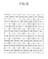
- FIG. 12 is a diagram concretely illustrating a display pattern in which a change in the voltage of the storage capacitor bus lines becomes a maximum.
- the storage capacitor bus lines 104 are arranged at right angles with the data bus lines 102 and, hence, parasitic capacitances Ck are formed at portions where the storage capacitor bus lines 104 intersect the data bus lines 102 . Therefore, a change in the voltage of the data bus lines 102 is transmitted to the storage capacitor bus lines 104 via the parasitic capacitances Ck. As a result, noise mixes into the storage capacitor bus lines 104 causing the voltage of the storage capacitor bus lines 104 to fluctuate. The voltage of the pixel electrodes 109 fluctuates accompanying a fluctuation in the voltage of the storage capacitor bus lines 104 , and there occurs display unevenness.
- the voltage of the storage capacitor bus lines 104 fluctuates like the above even due to a change in the signal voltage applied to the pixel electrodes 109 through the TFTs 108 , often causing display unevenness.
- This invention was accomplished in order to solve the above problem, and provides a liquid crystal display panel which is capable of reducing the voltage fluctuation on the storage capacitor bus lines and of preventing degradation in the quality of display.
- this invention is concerned with a liquid crystal display panel comprising pixel regions arranged like a matrix on a substrate, storage capacitors formed in the pixel regions, storage capacitor bus lines connected to the plurality of the storage capacitors, a common storage capacitor bus line for applying a predetermined potential to the plurality of the storage capacitor bus lines, and auxiliary capacitors connected to the common storage capacitor bus line.
- the auxiliary capacitors are formed by utilizing the common storage capacitor bus line.
- the storage capacitors and the auxiliary capacitors are formed in an MOS structure.
- the storage capacitors are formed in an n-MOS structure, and the auxiliary capacitors are formed in a p-MOS structure.
- the storage capacitors are formed in a p-MOS structure, and the auxiliary capacitors are formed in an n-MOS structure.
- auxiliary capacitors for stabilizing the voltage are added to the common storage capacitor bus line that applies a predetermined potential to the storage capacitor bus lines.
- the auxiliary capacitors for stabilizing the voltage absorb noises that are mixed into the storage capacitor bus lines via parasitic capacitances at portions where the data bus lines are intersecting the storage capacitor bus lines. Even when the voltage of the storage capacitor bus lines fluctuates accompanying the fluctuation of the signal voltage applied to the pixel electrodes, the fluctuation of the voltage can be absorbed by the auxiliary capacitors for stabilizing the voltage. This suppresses the fluctuation in the voltage of the storage capacitor bus lines and, hence, prevents the occurrence of display unevenness and the transverse crosstalk, making it possible to obtain a display of good quality.
- the auxiliary capacitor for stabilizing the voltage that is added to the common storage capacitor bus line is formed in the MOS structure, too, to further increase the auxiliary capacitor for stabilizing the voltage and, hence, to effectively suppress the fluctuation in the voltage of the storage capacitor bus line.
- the auxiliary capacitor for stabilizing the voltage is formed in the p-MOS structure and when the storage capacitor in the pixel is formed in the p-MOS structure, the capacitance for stabilizing the voltage is formed in the n-MOS structure, so that the voltage supplied to the common storage capacitor bus line is used as an off-voltage or an on-voltage for the gate bus lines. This eliminates the need of newly supplying a voltage, and the circuit constitution and the structure of the liquid crystal display panel can be simplified.
- FIG. 1 is a diagram of an equivalent circuit of a liquid crystal display panel according to an embodiment of the invention.
- FIG. 2 is a diagram of an equivalent circuit of another liquid crystal display panel according to the embodiment of the invention.
- FIG. 3 is a diagram of a wiring constitution of major portions in the liquid crystal display panel according to the first embodiment of the invention.
- FIG. 4A is a sectional view of a pixel region (along the line A—A in FIG. 3 ), and FIG. 4B is a sectional view of a capacitor portion (along the line B—B in FIG. 3 ) formed by utilizing a common storage capacitor bus line;
- FIG. 5 is a diagram of a wiring constitution of major portions in the liquid crystal display panel according to a second embodiment of the invention.
- FIG. 6A is a sectional view of a pixel region (along the line C—C in FIG. 5 ), and FIG. 6B is a sectional view of a capacitor portion (along the line D—D in FIG. 5 ) formed by utilizing the common storage capacitor bus line;
- FIG. 7 is a diagram of a wiring constitution of major portions in the liquid crystal display panel according to a third embodiment of the invention.
- FIG. 8 is a diagram of a wiring constitution of major portions in the liquid crystal display panel according to the third embodiment of the invention.
- FIG. 9 is a diagram of an equivalent circuit of a conventional liquid crystal display panel
- FIG. 10 is a diagram of an equivalent circuit of a display pixel in the conventional liquid crystal display panel
- FIGS. 11A and 11B are diagrams showing a problem inherent in the conventional liquid crystal display panel, wherein FIG. 11A is a diagram of an equivalent circuit illustrating parasitic capacitances Ck formed at portions where the storage capacitor bus lines intersect the data bus lines (signal lines), and noises mixing into the storage capacitor bus lines through the parasitic capacitances Ck, and FIG. 11B is a diagram illustrating a change in the signal voltage of the data bus lines (signal lines); and
- FIG. 12 is a diagram illustrating the problem inherent in the conventional liquid crystal display panel, and concretely illustrating a display pattern in which voltage fluctuation becomes a maximum on the storage capacitor bus lines.
- FIG. 1 is a diagram of an equivalent circuit of the liquid crystal display panel according to the embodiment.
- a plurality of data bus lines (signal lines) 2 are formed in parallel on one transparent glass substrate that is not shown, and a plurality of gate bus lines (scanning lines) 3 are formed thereon in an intersecting manner via an insulating film that is not shown.
- a plurality of storage capacitor bus lines (storage capacitor bus lines for each of the rows: horizontal storage capacitor bus lines) 4 are arranged in parallel with the gate bus lines 3 , and a common storage capacitor bus line 5 is arranged at the ends on one side of the storage capacitor bus lines 4 in parallel with the data bus lines 2 .
- the storage capacitor bus lines (for each of the rows) 4 are electrically connected to the common storage capacitor bus line 5 .
- a predetermined potential (storage capacitor bus line voltage Vcs) is supplied from a storage capacitor bus line drive circuit (not shown) to the storage capacitor bus lines (storage capacitor bus lines for each of the rows: horizontal storage capacitor bus lines) 4 through the common storage capacitor bus line (vertical storage capacitor bus line) 5 .
- Pixels are formed in the regions defined by the data bus lines 2 and by the gate bus lines 3 .
- Data drivers (signal line drive circuits) 6 and gate drivers (scanning line drive circuits) 7 are provided on the peripheral regions of the display region on one transparent glass substrate (not shown) on where the pixels are formed to drive the data bus lines 2 and the gate bus lines 3 .
- Thin-film transistors (TFTs) 8 are formed near the points where the data bus lines 2 and the gate bus lines 3 intersect each other.
- the drain electrode D of the TFT 8 is connected to the data bus line 2
- the gate electrode G of the TFT 8 is connected to the gate bus line 3
- the source electrode S of the TFT 8 is connected to a pixel electrode 9 .
- a liquid crystal layer 11 is held between the pixel electrode 9 and an opposing electrode 10 thereby to form a liquid crystal capacitance Clc.
- a storage capacitor Cs is connected in parallel with the liquid crystal capacitance Clc.
- the storage capacitor Cs is formed between the pixel electrode 9 and the storage capacitor bus line 4 .
- the opposing electrode 10 is formed on the other transparent glass substrate that is not shown. An opposing electrode voltage Vcom is supplied to the opposing electrode 10 .
- auxiliary capacitors Ccs for stabilizing the voltage are connected to the common storage capacitor bus line (vertical storage capacitor bus line) 5 .
- the auxiliary capacitors Ccs for stabilizing the voltage are provided for each of the horizontal storage capacitor bus lines of each of the rows.
- a predetermined potential (voltage on the side of common electrodes of the auxiliary capacitors for stabilizing voltage: Vccs) is applied to the ends on the other side (common side) of the auxiliary capacitors Ccs for stabilizing the voltage.
- the predetermined potential voltage on the side of common electrodes of the auxiliary capacitors for stabilizing voltage: Vccs
- Vccs the ground potential or a potential which is higher than the storage capacitor bus line voltage Vcs by about 3 V. It is desired that the capacitance of the auxiliary capacitor Ccs for stabilizing the voltage is greater than the total capacitance of a row of storage capacitors Cs. To increase the capacitance of the auxiliary capacitor Ccs for stabilizing the voltage, however, a wide region is necessary for forming the auxiliary capacitor Ccs for stabilizing the voltage. Therefore, the capacitance of the auxiliary capacitor Ccs for stabilizing the voltage may be smaller than the total capacitance of the row of storage capacitors Cs.
- auxiliary capacitors Ccs for stabilizing the voltage are connected to the common storage capacitor bus line 5 to absorb noise that has mixed into the storage capacitor bus lines 4 and to stabilize the voltages of the storage capacitor bus lines 4 .
- voltage fluctuation on the pixel electrodes 9 decreases and, as a result, occurrence of crosstalk in the transverse direction is prevented on the display region.
- FIG. 2 is a diagram of an equivalent circuit of another liquid crystal display panel according to the embodiment.
- the liquid crystal display panel 21 shown in FIG. 2 is fabricated by a process for producing polysilicon at low temperatures, and the constitution of a portion surrounded by a dotted line, except the opposing electrodes 10 , is formed on one transparent glass substrate that is not shown.
- the liquid crystal display panel 21 includes a plurality of data bus lines 2 a to 2 n and a plurality of gate bus lines 3 a to 3 i formed intersecting each other via an insulating film on one transparent glass substrate that is not shown.
- storage capacitor bus lines (storage capacitor bus lines for each of the rows: horizontal storage capacitor bus lines) 4 a to 4 i are formed in parallel with the gate bus lines 3 a to 3 i .
- common storage capacitor bus lines 5 L and 5 R are formed on the right and left sides of the ends of the storage capacitor bus lines 4 a to 4 i .
- the storage capacitor bus lines 4 are electrically connected to the common storage capacitor bus lines 5 L and 5 R.
- a predetermined potential (storage capacitor bus line voltage Vcs) is applied from an storage capacitor bus line drive circuit that is not shown to the storage capacitor bus lines 4 a to 4 i through the right and left common storage capacitor bus lines (vertical storage capacitor bus lines) 5 R and 5 L.
- Auxiliary capacitors CcsL, CcsR for stabilizing the voltage are connected to the common storage capacitor bus lines 5 L and 5 R.
- the auxiliary capacitors CcsL, CcsR for stabilizing the voltage are provided for the storage capacitor bus lines 4 a to 4 i of each of the rows.
- Pixels are formed in the regions defined by the data bus lines 2 a to 2 n and by the gate bus lines 3 a to 3 i .
- Analog switching circuits (SW) 22 a to 22 n are formed on the region on, for example, the upper side in the periphery of the display region where the pixels are formed on one transparent glass substrate that is not shown, the number of the analog switching circuits (SW) 22 a to 22 n being equal to the total number of the data bus lines 2 a to 2 n .
- first and second data drivers (signal line drive circuits) 6 a and 6 b , as well as a data bus line selection control circuit (not shown) for forming and outputting data bus line selection control signals RC 1 to RCm for controlling the selection of the data bus lines 2 a to 2 n for applying half-tone voltages output from the data drivers 6 a and 6 b.
- the half-tone voltage output from the first data driver 6 a is applied to the input terminals of the analog switching circuits 22 a , - - - , 22 n ⁇ 1 of odd numbers.
- the half-tone voltage output from the second data driver 6 b is applied to the input terminals of the analog switching circuits 22 b , - - - , 22 n of even numbers.
- the output terminal of the first analog switching circuit 22 a is connected to the first data bus line 2 a .
- the output terminals of the second, - - - , (n ⁇ 1)th and n-th analog switching circuits 22 b , - - - , 22 n ⁇ 1, 22 n are connected to the second, - - - , (n ⁇ 1)th and n-th data bus lines 2 b , - - - , 2 n ⁇ 1 and 2 n .
- a first data bus line selection control signal RC 1 is applied to the switching control terminals of the first and second analog switching circuits 22 a and 22 b .
- the first and second analog switching circuits 22 a and 22 b are rendered conductive, the half-tone voltage output from the first data driver 6 a is applied to the first data bus line 2 a , and the half-tone voltage output from the second data driver 6 b is applied to the second data bus line 2 b .
- the (n ⁇ 1)th and n-th analog switching circuits 22 n ⁇ 1 and 22 n are rendered conductive, the half-tone voltage output from the first data driver 6 a is applied to the (n ⁇ 1) th data bus line 2 n ⁇ 1, and the half-tone voltage output from the second data driver 6 b is applied to the n-th data bus line 2 n.
- analog switching circuits 22 a to 22 n are provided between the data drivers 6 a , 6 b and the data bus lines 2 a to 2 n to apply the half-tone voltage to the data bus lines 2 a to 2 n in a time-divisional manner while decreasing the number of the signal lines between the liquid crystal display panel 21 and the data drive circuit board provided on the outside of the liquid crystal display panel 21 .
- FIG. 2 illustrates the constitution in which the half-tone voltage is applied to the two data bus lines simultaneously, it is also allowable to apply the half-tone voltage to three or more data bus lines simultaneously.
- the shift registers 24 L and 24 R form vertical scanning signals (gate drive signals) based upon the vertical scanning control signal SC.
- the vertical scanning signals (gate drive signals) output from one shift register 24 L are applied to the gate bus lines 3 a to 3 i through the gate buffer circuits 24 La to 24 Li.
- the vertical scanning signals (gate drive signals) output from the other shift register 24 R are applied to the gate bus lines 3 a to 3 i through the gate buffer circuits 24 Ra to 24 Ri.
- the scanning signals are applied to one gate bus line 3 through both the right and left ends thereof, so that the scanning signals will not become dull even in a large liquid crystal display panel in which there are many pixels in the horizontal direction (transverse direction) and the gate bus lines are long.
- the pixels are formed in the regions defined by the data bus lines 2 and the gate bus lines 3 .
- the pixels are constituted in the same manner as those of the liquid crystal display device 1 shown in FIG. 1 , and are each provided with the thin-film transistor (TFT) 8 , the liquid crystal capacitance Clc and the storage capacitor Cs.
- TFT thin-film transistor
- auxiliary capacitors CcsL, CcsR for stabilizing the voltage are connected to the common storage capacitor bus lines (vertical storage capacitor bus lines) 5 L and 5 R.
- the auxiliary capacitors CcsL, CcsR for stabilizing the voltage are provide for the horizontal storage capacitor bus lines of each of the rows.
- a predetermined potential (voltage on the side of the common electrodes of the auxiliary capacitors for stabilizing voltage: Vccs) is applied to the other ends (common side) of the auxiliary capacitors CcsL, CcsR for stabilizing the voltage.
- the predetermined potential voltage on the side of the common electrodes of the auxiliary capacitors for stabilizing voltage: Vccs
- the auxiliary capacitors CcsR, CcsL for stabilizing the voltage are connected to the right and left common storage capacitor bus lines 5 R and 5 L. Therefore, it is desired that the capacitances of the auxiliary capacitors CcsL and CcsR for stabilizing the voltage are not smaller than one-half the total capacitance of a row of the storage capacitors Cs.
- the capacitances of the auxiliary capacitors CcsL, CcsR for stabilizing the voltage may be smaller than one-half the total capacitance of the row of the storage capacitors Cs.
- auxiliary capacitors CcsL, CcsR for stabilizing the voltage are connected to the common storage capacitor bus lines 5 L, 5 R to absorb noise that has mixed into the storage capacitor bus lines 4 a to 4 i and to stabilize the voltages of the storage capacitor bus lines 4 a to 4 i .
- voltage fluctuation on the pixel electrodes 9 decreases and, as a result, occurrence of crosstalk in the transverse direction is prevented.
- FIG. 3 is a diagram of a wiring constitution of major portions in the liquid crystal display panel according to the first embodiment
- FIG. 4A is a sectional view of a pixel region (along the line A—A in FIG. 3 )
- FIG. 4B is a sectional view of a capacitor portion (along the line B—B in FIG. 3 ) formed by utilizing the common storage capacitor bus line.
- liquid crystal display panel 31 In the liquid crystal display panel 31 according to the first embodiment as shown in FIG. 3 , there are formed a plurality of gate bus lines 33 in parallel on the transparent glass substrate, and a plurality of data bus lines 32 intersecting thereto via an insulating film which is not shown. There are further formed a plurality of storage capacitor bus lines (horizontal Cs bus lines) 34 in parallel with the gate bus lines 33 , and a common storage capacitor bus line (vertical Cs bus line) 35 in parallel with the data bus lines 32 .
- horizontal Cs bus lines horizontal Cs bus lines
- vertical Cs bus line vertical Cs bus line
- TFTs 36 are arranged at positions near the points where the gate bus lines 33 intersect the data bus lines 32 .
- Pixel electrodes (transparent electrodes) 37 are arranged on the regions defined by the gate bus lines 33 and the data bus lines 32 .
- the drain electrodes of the TFTs 36 are connected to the data bus lines 32
- the source electrodes of the TFTs 36 are connected to the data layers 38 and are further connected to the pixel electrodes (transparent electrodes) 37 through the data layers 38 .
- the data layer 38 is extending up to a position where it is opposed to the storage capacitor bus line (horizontal Cs bus line) 34 . Referring to FIG.
- the storage capacitor bus line 34 and the data layer 38 are opposed to each other via a first interlayer film 39 thereby to form an storage capacitor Cs for each of the pixels.
- a region where the storage capacitor Cs is formed is surrounded by a dot-dash chain line.
- the region where the storage capacitor Cs is formed as surrounded by the dot-dash chain line is shown concerning a particular pixel only.
- a source region of a polysilicon layer 44 is connected to the source electrode of the TFT 36 through a contact hole 40 formed in the first interlayer film 39 (see FIG. 4 A). Further, the data layer 38 is connected to the pixel electrode (transparent electrode) 37 through a contact hole 41 formed in a second interlayer film 42 (see FIG. 4 A). The polysilicon layer 44 extending up to under the data bus line 32 is connected to the data bus line 32 through a contact hole 92 formed in the first interlayer film 39 .
- the pixel region is formed as described below.
- the polysilicon layer 44 is formed on the transparent glass substrate 43 .
- an oxide film 45 is formed on the polysilicon layer 44 .
- the gate bus line (gate layer) 33 and the storage capacitor bus line 34 are formed on the oxide film 45 .
- the first interlayer film 39 is formed on the gate bus line (gate layer) 33 and on the storage capacitor bus line 34 .
- the first interlayer film 39 on the polysilicon layer 44 is opened to form the contact hole 40 .
- the data layer 38 and the source electrode of the TFT 36 are formed on the first interlayer film 39 .
- the data layer 38 is formed on a region from the source electrode of the TFT 36 up to the storage capacitor bus line 34 .
- the storage capacitor bus line 34 and the data layer 38 are opposed to each other via the first interlayer film 39 to form the storage capacitor Cs.
- the second interlayer film 42 is formed on the data layer 38 and on the first interlayer film 39 , and the second interlayer film 42 on the data layer 38 is opened to form the contact hole 41 .
- the pixel electrode 37 is then formed on the second interlayer film 42 .
- a transparent glass substrate (not shown) equipped with an opposing electrode (not shown) is disposed to be opposed to the transparent glass substrate 43 .
- Liquid crystals are sealed among the transparent glass substrate (not shown) equipped with the opposing electrode (not shown), the pixel electrode 37 and the second interlayer film 42 to form a liquid crystal display portion.
- the auxiliary capacitor Ccs for stabilizing the voltage is formed for each of the storage capacitor bus lines (horizontal Cs bus lines) 34 by utilizing the common storage capacitor bus line 35 which is for applying the predetermined potential (Cs potential) to the storage capacitor bus lines (horizontal Cs bus lines) 34 .
- a Ccs wiring (gate layer) 46 which serves as one electrode of the auxiliary capacitor Ccs is formed on the transparent glass substrate 43 , the oxide film 45 is formed on the Ccs wiring (gate layer) 46 , and the common storage capacitor bus line 35 is formed on the oxide film 45 , thereby to form the auxiliary capacitor Ccs with the Ccs wiring (gate layer) 46 and the common storage capacitor bus line 35 being opposed to each other via the oxide film 45 .
- the first interlayer film 39 is formed on the common storage capacitor bus line 35 .
- the vertical Ccs wiring (data layer) 47 for applying a predetermined potential to the Ccs wiring (gate layer) 46 that serves as one electrode of the auxiliary capacitor Ccs.
- the vertical Ccs wiring 47 is connected to the Ccs wiring 46 through the contact hole 90 .
- the vertical Ccs wiring 47 is arranged by the side of the common storage capacitor wiring 35 in parallel with the common storage capacitor wiring 35 .
- the second interlayer film 42 is formed on the vertical Ccs wiring 47 and on the common storage capacitor wiring 35 .
- the Ccs wiring 46 of the auxiliary capacitor Ccs on the common side is formed on the transparent glass substrate 43 by using the gate layer, and the wiring of the common storage capacitor bus line 35 is formed with the first interlayer film 39 sandwiched therebetween, thereby to form the auxiliary capacitor Ccs that is added to the common storage capacitor bus line 35 . It is therefore allowed to add the auxiliary capacitor Ccs to the common storage capacitor bus line 35 without increasing the number of the steps for fabricating the liquid crystal display panel.
- the width of the common storage capacitor bus line 35 arranged in the vertical direction may be increased or the thickness of the first interlayer film 39 may be decreased.
- the common side of the auxiliary capacitor Ccs may be fixed to a predetermined potential. Therefore, there may be employed the same voltage as the power source voltage for the gate buffer or as that of the electrode (common electrode) opposing with the liquid crystals held therebetween.
- FIG. 5 is a diagram of a wiring constitution of major portions in the liquid crystal display panel according to a second embodiment of the invention
- FIG. 6A is a sectional view of a pixel region (along the line C—C in FIG. 5 )
- FIG. 6B is a sectional view of a capacitor portion (along the line D—D in FIG. 5 ) formed by utilizing the common storage capacitor bus line.
- liquid crystal display panel 51 In the liquid crystal display panel 51 according to the second embodiment as shown in FIG. 5 , there are formed a plurality of gate bus lines 53 in parallel on the transparent glass substrate, and a plurality of data bus lines 52 intersecting thereto via an insulating film which is not shown. There are further formed a plurality of storage capacitor bus lines (horizontal Cs bus lines) 54 in parallel with the gate bus lines 53 , and a common storage capacitor bus line (vertical Cs bus line) 55 in parallel with the data bus line 52 .
- horizontal Cs bus lines horizontal Cs bus lines
- vertical Cs bus line vertical Cs bus line
- TFTs 56 are arranged at positions near the points where the gate bus lines 53 intersect the data bus lines 52 .
- the drain electrodes of the TFTs 56 are connected to the data bus lines 52
- the source electrodes of the TFTs 56 are connected to the data layers 58 and are further connected to the pixel electrodes (transparent electrodes) 57 through the data layers 58 .
- Pixel electrodes (transparent electrodes) 57 are arranged in the regions defined by the gate bus lines 53 and by the data bus lines 52 .
- the data layer 58 is extending near to the storage capacitor bus line (horizontal Cs bus line) 54 .
- a source region of a polysilicon layer 64 a is connected to the source electrode of the TFT 56 through a contact hole 60 formed in the first interlayer film 59 (see FIG. 6 A). Further, the data layer 58 is connected to the pixel electrode (transparent electrode) 57 through a contact hole 61 formed in a second interlayer film 62 (see FIG. 6 A). The polysilicon layer 64 extending up to under the data bus line 52 is connected to the data bus line 52 through a contact hole 92 formed in the first interlayer film 59 .
- the pixel region is formed as described below.
- a polysilicon layer 64 a that serves as an operation semiconductor layer of the TFT 56 and a polysilicon layer 64 b that serves as one electrode of the storage capacitor Cs.
- oxide films 65 a , 65 b are formed on the polysilicon layers 64 a , 64 b , a gate bus line (gate layer) 53 is formed on the oxide film 65 a thereby to form the TFT 56 and, at the same time, the storage capacitor bus line 54 is formed on the oxide film 65 b .
- the storage capacitor Cs is formed as the polysilicon layer 64 b and the storage capacitor bus line 54 are disposed opposing each other via the oxide film 65 b .
- a region where the storage capacitor Cs is formed is surrounded by a dot-dash chain line.
- the region where the storage capacitor Cs is formed as surrounded by the dot-dash chain line is shown concerning a particular pixel only.
- the first interlayer film 59 is formed on the gate bus line 53 and on the storage capacitor bus line 54 . Then, the first interlayer film 59 on the polysilicon layer 64 a is opened to form the contact hole 60 . Then, the data layer 58 is formed on the first interlayer film 59 . The data layer 58 is formed on a region from the source electrode of the TFT 56 up to the storage capacitor bus line 54 . Then, the second interlayer film 62 is formed on the data layer 58 and on the first interlayer film 59 , and the second interlayer film 62 on the data layer 58 is opened to form the contact hole 61 . The pixel electrode 57 is then formed on the second interlayer film 62 .
- a transparent glass substrate (not shown) equipped with an opposing electrode (not shown) is disposed to be opposed to the transparent glass substrate 63 .
- Liquid crystals are sealed among the transparent glass substrate (not shown) equipped with the opposing electrode (not shown), the pixel electrode 57 and the second interlayer film 62 to form a liquid crystal display portion.
- the auxiliary capacitor Ccs for stabilizing the voltage is formed for each of the storage capacitor bus lines (horizontal Cs bus lines) 54 by utilizing the common storage capacitor bus line 55 which is for applying the predetermined potential (Cs potential) to the storage capacitor bus lines (horizontal Cs bus lines) 54 .
- a Ccs wiring (polysilicon layer) 66 which serves as one electrode of the auxiliary capacitor Ccs is formed on the transparent glass substrate 63 , the oxide film 65 c is formed on the Ccs wiring (polysilicon layer) 66 , and the common storage capacitor bus line (vertical Cs bus line)(gate layer) 55 is formed on the oxide film 65 c , thereby to form the auxiliary capacitor Ccs with the Ccs wiring (polysilicon layer) 66 and the common storage capacitor bus line 55 being opposed to each other via the oxide film 65 c .
- the first interlayer film 59 is formed on the common storage capacitor bus line 55 .
- the vertical Ccs wiring (data layer) for applying a predetermined potential to the Ccs wiring (data layer) 66 that serves as one electrode (common electrode) of the auxiliary capacitor Ccs.
- the vertical Ccs wiring 67 is connected to the Ccs wiring 66 through the contact hole 90 .
- the vertical Ccs wiring (data layer) 67 is arranged by the side of the common storage capacitor wiring 55 in parallel with the common storage capacitor wiring 55 .
- the second interlayer film 62 is formed on the vertical Ccs wiring 67 and on the common storage capacitor wiring 55 .
- the storage capacitors Cs of pixels and auxiliary capacitors Ccs added to the common storage capacitor bus line 55 are formed of MOS capacitors.
- the capacitance per a unit area can be increased compared to that of when the capacitor is formed by the gate layer, interlayer film and data layer as is done in the first embodiment.
- the potential difference between the polysilicon layer and the gate layer must be greater than a predetermined voltage (about 3 volts).
- a voltage higher than a maximum voltage of the pixel electrode must be applied.
- the MOS capacitor (Ccs) added to the common storage capacitor bus line 55 is formed of the n-MOS capacitor, it becomes necessary to apply a voltage which is higher than the voltage (Vcs) applied to the storage capacitor bus lines (Cs bus lines).
- This constitution is the one based on the polysilicon process.
- the above constitution is employed in the case of a single channel (n-MOS or p-MOS). In the case of amorphous silicon, the process is usually for the n-MOS only, and the same holds.
- FIG. 7 is a diagram of a wiring constitution of major portions in the liquid crystal display panel according to a third embodiment of the invention.
- the storage capacitor Cs of the pixel is formed of an MOS capacitor of n-CH (n-channel)
- the auxiliary capacitor Ccs added to the common storage capacitor bus line (vertical Cs bus line) 67 is formed of an MOS capacitor of p-CH (p-channel).
- the wiring structure of the liquid crystal display panel 71 shown in FIG. 7 is almost the same as the wiring structure of the liquid crystal display panel 51 shown in FIG.
- the polysilicon layer 72 which serves as one electrode of the storage capacitor Cs is formed of polysilicon of n-CH (n-channel) and the polysilicon layer 73 which serves as one electrode of the auxiliary capacitor Ccs added to the common storage capacitor bus line 67 is formed of polysilicon of p-CH (p-channel).
- the storage capacitor bus line voltage Vcs applied to the storage capacitor bus line (horizontal Cs bus line) 64 forming the other electrode of the storage capacitor Cs can be set to be a maximum voltage of the pixel electrode+about 3 volts
- the voltage Vccs applied to the common side of the auxiliary capacitors Ccs added to the common storage capacitor bus line 67 can be set to be the storage capacitor bus line voltage Vcs ⁇ about 3 volts.
- the off-voltage of the gate can be used as the voltage Vccs to be applied to the common side of the auxiliary capacitors Ccs, offering such a merit that the power source wiring of the gate buffer can be used in common and the wiring region can be decreased.
- FIG. 8 is a diagram of a wiring constitution of major portions in the liquid crystal display panel according to the third embodiment of the invention.
- the storage capacitor Cs of the pixel is formed of an MOS capacitor of p-CH (p-channel)
- the auxiliary capacitor Ccs added to the common storage capacitor bus line 67 is formed of an MOS capacitor of n-CH (n-channel).
- the wiring structure of the liquid crystal display panel 81 shown in FIG. 8 is almost the same as the wiring structure of the liquid crystal display panel 51 shown in FIG.
- the polysilicon layer 82 which serves as one electrode of the storage capacitor Cs is formed of polysilicon of p-CH (p-channel) and the polysilicon layer 83 which serves as one electrode of the auxiliary capacitor Ccs added to the common storage capacitor bus line 67 is formed of polysilicon of n-CH (n-channel).
- Whether the storage capacitor Cs be formed in the n-MOS structure or in the p-MOS structure, or whether the auxiliary capacitor Ccs to be added be formed in the p-MOS structure or the n-MOS structure, is suitably determined relying upon the layout constitution such as the power source wiring.
- the liquid crystal display device By constituting the liquid crystal display device by using the liquid crystal display panel 31 , 51 , 71 or 81 of the first to fourth embodiments, it is allowed to suppress the fluctuation in the voltage of the storage capacitor bus lines (horizontal Cs bus lines) even when there is displayed a pattern which is likely to develop display unevenness or crosstalk as shown in, for example, FIG. 14 . Therefore, there can be displayed images of a high quality without developing display unevenness or crosstalk.
- polysilicon layers 44 and 64 a were used as the operation semiconductor layers of the TFTs 8 , 36 and 56 .
- the amorphous silicon layer as the operation semiconductor layer for the TFTs 8 , 36 and 56 .
- the liquid crystal display panel of this invention is of the active matrix drive type in which each pixel is provided with an storage capacitor, and wherein auxiliary capacitors for stabilizing the voltage are added to the common storage capacitor bus line that applies a predetermined potential to the storage capacitor bus lines provided for each of the rows. Therefore, the auxiliary capacitors for stabilizing the voltage absorb noises mixed into the storage capacitor bus lines through parasitic capacitances formed at portions where the data bus lines intersect the storage capacitor bus lines. Further, even when the voltage of the storage capacitor bus lines has fluctuated accompanying a change in the signal voltage applied to the pixel electrodes, the fluctuation in the voltage can be absorbed by the auxiliary capacitors for stabilizing the voltage. Thus, the fluctuation in the voltage of the storage capacitor bus lines is suppressed, preventing the occurrence of display unevenness or crosstalk in the transverse direction, and presenting display of good quality.
- the auxiliary capacitor for stabilizing voltage added to the common storage capacitor bus line is formed in the MOS structure, too, making it possible to further increase the auxiliary capacitor for stabilizing the voltage and to effectively suppress the fluctuation in the voltage of the storage capacitor bus lines.
- the auxiliary capacitor for stabilizing the voltage is formed in the p-MOS structure.
- the auxiliary capacitor for stabilizing the voltage is formed in the n-MOS structure. Therefore, the voltage applied to the common storage capacitor bus line can be used as the off-voltage or the on-voltage for the gate bus line. This eliminates the need of newly applying the voltage, and the circuit constitution and the structure of the liquid crystal display panel can be simplified.
Landscapes
- Physics & Mathematics (AREA)
- Nonlinear Science (AREA)
- Engineering & Computer Science (AREA)
- Mathematical Physics (AREA)
- Chemical & Material Sciences (AREA)
- Crystallography & Structural Chemistry (AREA)
- General Physics & Mathematics (AREA)
- Optics & Photonics (AREA)
- Power Engineering (AREA)
- Microelectronics & Electronic Packaging (AREA)
- Liquid Crystal (AREA)
- Devices For Indicating Variable Information By Combining Individual Elements (AREA)
Abstract
Description
Claims (6)
Priority Applications (1)
| Application Number | Priority Date | Filing Date | Title |
|---|---|---|---|
| AU2003252848A AU2003252848B2 (en) | 2002-10-09 | 2003-10-07 | Device for distracting vertebrae and delivering a flowable material into a disc space |
Applications Claiming Priority (2)
| Application Number | Priority Date | Filing Date | Title |
|---|---|---|---|
| JP2002000149A JP3992984B2 (en) | 2002-01-04 | 2002-01-04 | LCD panel |
| JP2002-000149 | 2002-01-04 |
Publications (2)
| Publication Number | Publication Date |
|---|---|
| US20030128306A1 US20030128306A1 (en) | 2003-07-10 |
| US6873378B2 true US6873378B2 (en) | 2005-03-29 |
Family
ID=19190448
Family Applications (1)
| Application Number | Title | Priority Date | Filing Date |
|---|---|---|---|
| US10/267,613 Expired - Lifetime US6873378B2 (en) | 2002-01-04 | 2002-10-09 | Liquid crystal display panel |
Country Status (5)
| Country | Link |
|---|---|
| US (1) | US6873378B2 (en) |
| JP (1) | JP3992984B2 (en) |
| KR (1) | KR100812479B1 (en) |
| CN (1) | CN1251171C (en) |
| TW (1) | TWI307074B (en) |
Cited By (7)
| Publication number | Priority date | Publication date | Assignee | Title |
|---|---|---|---|---|
| US20060146260A1 (en) * | 2005-01-03 | 2006-07-06 | Samsung Electronics Co., Ltd. | Array substrate and display panel having the same |
| US20060238667A1 (en) * | 2005-04-22 | 2006-10-26 | Woo-Geun Lee | Thin film transistor substrate, method of manufacturing the same and display apparatus having the same |
| US20090168004A1 (en) * | 2006-01-16 | 2009-07-02 | Samsung Electronics Co., Ltd. | Liquid crystal display panel and manufacturing method thereof |
| US20100177026A1 (en) * | 2007-07-03 | 2010-07-15 | Liquavista B.V. | Electrowetting system and method for operating |
| US20110007059A1 (en) * | 2005-02-07 | 2011-01-13 | Samsung Electronics Co., Ltd. | Liquid crystal display and driving method thereof |
| US20110187696A1 (en) * | 2008-08-01 | 2011-08-04 | Liquavista B.V. | Electrowetting system |
| US12051370B2 (en) | 2021-02-02 | 2024-07-30 | Google Llc | Power line design modification to mitigate vertical band crosstalk |
Families Citing this family (14)
| Publication number | Priority date | Publication date | Assignee | Title |
|---|---|---|---|---|
| JP4269582B2 (en) * | 2002-05-31 | 2009-05-27 | ソニー株式会社 | Liquid crystal display device, control method thereof, and portable terminal |
| JP4352937B2 (en) * | 2004-03-03 | 2009-10-28 | セイコーエプソン株式会社 | Power supply circuit, electro-optical device and electronic apparatus |
| KR101026982B1 (en) * | 2004-06-03 | 2011-04-11 | 엘지디스플레이 주식회사 | Array Substrate for LCD and Manufacturing Method |
| KR101100882B1 (en) * | 2004-11-05 | 2012-01-02 | 삼성전자주식회사 | Liquid crystal display and its driving device |
| JP2006154088A (en) * | 2004-11-26 | 2006-06-15 | Sanyo Electric Co Ltd | Active matrix type liquid crystal display device |
| CN100461248C (en) * | 2005-09-29 | 2009-02-11 | 中华映管股份有限公司 | common voltage correction circuit and method |
| KR20080009889A (en) * | 2006-07-25 | 2008-01-30 | 삼성전자주식회사 | Liquid crystal display |
| KR101374088B1 (en) * | 2007-03-08 | 2014-03-14 | 삼성디스플레이 주식회사 | Array substrate and display panel having the same |
| US8791928B2 (en) * | 2007-11-06 | 2014-07-29 | Hannstar Display Corp. | Pixel driving method, pixel driving device and liquid crystal display using thereof |
| US9261741B2 (en) * | 2009-12-04 | 2016-02-16 | Sharp Kabushiki Kaisha | Liquid crystal display device including trunk lines |
| KR101696393B1 (en) | 2010-06-15 | 2017-01-16 | 삼성디스플레이 주식회사 | Display panel |
| WO2013065529A1 (en) * | 2011-10-31 | 2013-05-10 | シャープ株式会社 | Thin film transistor array substrate and liquid crystal display device |
| CN104142591B (en) * | 2014-07-11 | 2017-07-18 | 合肥鑫晟光电科技有限公司 | A kind of array base palte and preparation method, a kind of display device |
| CN115793302A (en) * | 2022-11-30 | 2023-03-14 | 惠科股份有限公司 | Common electrode output circuit, display panel and display device |
Citations (3)
| Publication number | Priority date | Publication date | Assignee | Title |
|---|---|---|---|---|
| US5734450A (en) * | 1995-03-17 | 1998-03-31 | Sharp Kabushiki Kaisha | Active-matrix substrate and a defect correcting method thereof |
| US5748266A (en) * | 1995-03-10 | 1998-05-05 | International Business Machines Corporation | Color filter, liquid crystal display panel, liquid crystal display, and liquid crystal display panel manufacturing method |
| US5936686A (en) * | 1996-03-28 | 1999-08-10 | Kabushiki Kaisha Toshiba | Active matrix type liquid crystal display |
Family Cites Families (1)
| Publication number | Priority date | Publication date | Assignee | Title |
|---|---|---|---|---|
| KR100604268B1 (en) * | 1999-06-03 | 2006-07-24 | 엘지.필립스 엘시디 주식회사 | Active Matrix Liquid Crystal Display and Driving Method |
-
2002
- 2002-01-04 JP JP2002000149A patent/JP3992984B2/en not_active Expired - Fee Related
- 2002-09-26 TW TW091122191A patent/TWI307074B/en not_active IP Right Cessation
- 2002-10-09 US US10/267,613 patent/US6873378B2/en not_active Expired - Lifetime
- 2002-10-10 KR KR1020020061695A patent/KR100812479B1/en not_active Expired - Fee Related
- 2002-10-29 CN CNB021461260A patent/CN1251171C/en not_active Expired - Fee Related
Patent Citations (3)
| Publication number | Priority date | Publication date | Assignee | Title |
|---|---|---|---|---|
| US5748266A (en) * | 1995-03-10 | 1998-05-05 | International Business Machines Corporation | Color filter, liquid crystal display panel, liquid crystal display, and liquid crystal display panel manufacturing method |
| US5734450A (en) * | 1995-03-17 | 1998-03-31 | Sharp Kabushiki Kaisha | Active-matrix substrate and a defect correcting method thereof |
| US5936686A (en) * | 1996-03-28 | 1999-08-10 | Kabushiki Kaisha Toshiba | Active matrix type liquid crystal display |
Cited By (13)
| Publication number | Priority date | Publication date | Assignee | Title |
|---|---|---|---|---|
| US7483107B2 (en) * | 2005-01-03 | 2009-01-27 | Samsung Electronics Co., Ltd. | Array substrate and display panel having the same |
| US20060146260A1 (en) * | 2005-01-03 | 2006-07-06 | Samsung Electronics Co., Ltd. | Array substrate and display panel having the same |
| US20110007059A1 (en) * | 2005-02-07 | 2011-01-13 | Samsung Electronics Co., Ltd. | Liquid crystal display and driving method thereof |
| US8629820B2 (en) * | 2005-02-07 | 2014-01-14 | Samsung Display Co., Ltd. | Liquid crystal display and driving method thereof |
| US7369188B2 (en) * | 2005-04-22 | 2008-05-06 | Samsung Electronics Co., Ltd. | Thin film transistor substrate having two storage capacitors per pixel, method of manufacturing the same and display apparatus having the same |
| US20060238667A1 (en) * | 2005-04-22 | 2006-10-26 | Woo-Geun Lee | Thin film transistor substrate, method of manufacturing the same and display apparatus having the same |
| US20090168004A1 (en) * | 2006-01-16 | 2009-07-02 | Samsung Electronics Co., Ltd. | Liquid crystal display panel and manufacturing method thereof |
| US20100177026A1 (en) * | 2007-07-03 | 2010-07-15 | Liquavista B.V. | Electrowetting system and method for operating |
| US8791891B2 (en) | 2007-07-03 | 2014-07-29 | Liquavista B.V. | Electrowetting system and method for operating |
| US9052501B2 (en) | 2007-07-03 | 2015-06-09 | Amazon Technologies, Inc. | Electrowetting system and method for operating |
| US20110187696A1 (en) * | 2008-08-01 | 2011-08-04 | Liquavista B.V. | Electrowetting system |
| US8659587B2 (en) | 2008-08-01 | 2014-02-25 | Liquavista, B.V. | Electrowetting system |
| US12051370B2 (en) | 2021-02-02 | 2024-07-30 | Google Llc | Power line design modification to mitigate vertical band crosstalk |
Also Published As
| Publication number | Publication date |
|---|---|
| KR20030060052A (en) | 2003-07-12 |
| JP3992984B2 (en) | 2007-10-17 |
| TWI307074B (en) | 2009-03-01 |
| JP2003202592A (en) | 2003-07-18 |
| KR100812479B1 (en) | 2008-03-10 |
| CN1430199A (en) | 2003-07-16 |
| US20030128306A1 (en) | 2003-07-10 |
| CN1251171C (en) | 2006-04-12 |
Similar Documents
| Publication | Publication Date | Title |
|---|---|---|
| US6873378B2 (en) | Liquid crystal display panel | |
| KR100443219B1 (en) | Active matrix device and display | |
| US6982690B2 (en) | Display apparatus with a driving circuit in which every three adjacent pixels are coupled to the same data line | |
| US8035596B2 (en) | Liquid crystal display device | |
| US20010015710A1 (en) | Active matrix type liquid-crystal display unit and method of driving the same | |
| KR100268818B1 (en) | Active matrix liquid crystal display | |
| US6731260B2 (en) | Display device | |
| US8081148B2 (en) | Display device | |
| US6825822B2 (en) | Display apparatus with a time domain multiplex driving circuit | |
| US6828734B2 (en) | Display device | |
| KR100472269B1 (en) | Active matrix type display device | |
| KR100516091B1 (en) | Display device | |
| US6603455B1 (en) | Display panel drive circuit and display panel | |
| KR100571032B1 (en) | LCD Display | |
| KR20020010320A (en) | circuit for controlling common voltage in the Liquid Crystal Display | |
| US6683593B2 (en) | Liquid crystal display | |
| JP2517842B2 (en) | Display device | |
| JPH1090712A (en) | Liquid crystal display | |
| JP4455714B2 (en) | Thin film transistor substrate and liquid crystal display panel using the same | |
| JP4133499B2 (en) | Liquid crystal display | |
| JPH1090718A (en) | Liquid crystal display | |
| JPH10274762A (en) | Liquid crystal display device with built-in driving circuit | |
| JP3436753B2 (en) | Liquid crystal matrix display device and driving method thereof | |
| JP2004151716A (en) | Display device | |
| JP2000330138A (en) | Liquid crystal matrix display device and driving method thereof |
Legal Events
| Date | Code | Title | Description |
|---|---|---|---|
| AS | Assignment |
Owner name: FUJITSU DISPLAY TECHNOLOGIES CORPORATION, JAPAN Free format text: ASSIGNMENT OF ASSIGNORS INTEREST;ASSIGNOR:KAI, TSUTOMU;REEL/FRAME:013381/0723 Effective date: 20020708 |
|
| STCF | Information on status: patent grant |
Free format text: PATENTED CASE |
|
| AS | Assignment |
Owner name: FUJITSU LIMITED,JAPAN Free format text: ASSIGNMENT OF ASSIGNORS INTEREST;ASSIGNOR:FUJITSU DISPLAY TECHNOLOGIES CORPORATION;REEL/FRAME:016345/0310 Effective date: 20050630 Owner name: FUJITSU LIMITED, JAPAN Free format text: ASSIGNMENT OF ASSIGNORS INTEREST;ASSIGNOR:FUJITSU DISPLAY TECHNOLOGIES CORPORATION;REEL/FRAME:016345/0310 Effective date: 20050630 |
|
| AS | Assignment |
Owner name: SHARP KABUSHIKI KAISHA,JAPAN Free format text: ASSIGNMENT OF ASSIGNORS INTEREST;ASSIGNOR:FUJITSU LIMITED;REEL/FRAME:016345/0210 Effective date: 20050701 Owner name: SHARP KABUSHIKI KAISHA, JAPAN Free format text: ASSIGNMENT OF ASSIGNORS INTEREST;ASSIGNOR:FUJITSU LIMITED;REEL/FRAME:016345/0210 Effective date: 20050701 |
|
| CC | Certificate of correction | ||
| FEPP | Fee payment procedure |
Free format text: PAYOR NUMBER ASSIGNED (ORIGINAL EVENT CODE: ASPN); ENTITY STATUS OF PATENT OWNER: LARGE ENTITY |
|
| FPAY | Fee payment |
Year of fee payment: 4 |
|
| FPAY | Fee payment |
Year of fee payment: 8 |
|
| FEPP | Fee payment procedure |
Free format text: PAYOR NUMBER ASSIGNED (ORIGINAL EVENT CODE: ASPN); ENTITY STATUS OF PATENT OWNER: LARGE ENTITY Free format text: PAYER NUMBER DE-ASSIGNED (ORIGINAL EVENT CODE: RMPN); ENTITY STATUS OF PATENT OWNER: LARGE ENTITY |
|
| FPAY | Fee payment |
Year of fee payment: 12 |