US6825822B2 - Display apparatus with a time domain multiplex driving circuit - Google Patents
Display apparatus with a time domain multiplex driving circuit Download PDFInfo
- Publication number
- US6825822B2 US6825822B2 US10/212,124 US21212402A US6825822B2 US 6825822 B2 US6825822 B2 US 6825822B2 US 21212402 A US21212402 A US 21212402A US 6825822 B2 US6825822 B2 US 6825822B2
- Authority
- US
- United States
- Prior art keywords
- pixel
- scan line
- coupled
- switch
- line
- Prior art date
- Legal status (The legal status is an assumption and is not a legal conclusion. Google has not performed a legal analysis and makes no representation as to the accuracy of the status listed.)
- Expired - Lifetime, expires
Links
- 239000010409 thin film Substances 0.000 claims description 120
- 238000000034 method Methods 0.000 claims description 38
- 239000004973 liquid crystal related substance Substances 0.000 claims description 10
- 239000011159 matrix material Substances 0.000 description 12
- 230000003247 decreasing effect Effects 0.000 description 7
- 238000010586 diagram Methods 0.000 description 7
- 239000003990 capacitor Substances 0.000 description 6
- 230000000694 effects Effects 0.000 description 5
- 230000005669 field effect Effects 0.000 description 2
- 238000012986 modification Methods 0.000 description 2
- 230000004048 modification Effects 0.000 description 2
- 230000008878 coupling Effects 0.000 description 1
- 238000010168 coupling process Methods 0.000 description 1
- 238000005859 coupling reaction Methods 0.000 description 1
- 230000002349 favourable effect Effects 0.000 description 1
- 230000005855 radiation Effects 0.000 description 1
Images


Classifications
-
- G—PHYSICS
- G09—EDUCATION; CRYPTOGRAPHY; DISPLAY; ADVERTISING; SEALS
- G09G—ARRANGEMENTS OR CIRCUITS FOR CONTROL OF INDICATING DEVICES USING STATIC MEANS TO PRESENT VARIABLE INFORMATION
- G09G3/00—Control arrangements or circuits, of interest only in connection with visual indicators other than cathode-ray tubes
- G09G3/20—Control arrangements or circuits, of interest only in connection with visual indicators other than cathode-ray tubes for presentation of an assembly of a number of characters, e.g. a page, by composing the assembly by combination of individual elements arranged in a matrix no fixed position being assigned to or needed to be assigned to the individual characters or partial characters
- G09G3/34—Control arrangements or circuits, of interest only in connection with visual indicators other than cathode-ray tubes for presentation of an assembly of a number of characters, e.g. a page, by composing the assembly by combination of individual elements arranged in a matrix no fixed position being assigned to or needed to be assigned to the individual characters or partial characters by control of light from an independent source
- G09G3/36—Control arrangements or circuits, of interest only in connection with visual indicators other than cathode-ray tubes for presentation of an assembly of a number of characters, e.g. a page, by composing the assembly by combination of individual elements arranged in a matrix no fixed position being assigned to or needed to be assigned to the individual characters or partial characters by control of light from an independent source using liquid crystals
- G09G3/3611—Control of matrices with row and column drivers
- G09G3/3648—Control of matrices with row and column drivers using an active matrix
- G09G3/3659—Control of matrices with row and column drivers using an active matrix the addressing of the pixel involving the control of two or more scan electrodes or two or more data electrodes, e.g. pixel voltage dependant on signal of two data electrodes
-
- G—PHYSICS
- G09—EDUCATION; CRYPTOGRAPHY; DISPLAY; ADVERTISING; SEALS
- G09G—ARRANGEMENTS OR CIRCUITS FOR CONTROL OF INDICATING DEVICES USING STATIC MEANS TO PRESENT VARIABLE INFORMATION
- G09G2300/00—Aspects of the constitution of display devices
- G09G2300/08—Active matrix structure, i.e. with use of active elements, inclusive of non-linear two terminal elements, in the pixels together with light emitting or modulating elements
- G09G2300/0809—Several active elements per pixel in active matrix panels
- G09G2300/0814—Several active elements per pixel in active matrix panels used for selection purposes, e.g. logical AND for partial update
-
- G—PHYSICS
- G09—EDUCATION; CRYPTOGRAPHY; DISPLAY; ADVERTISING; SEALS
- G09G—ARRANGEMENTS OR CIRCUITS FOR CONTROL OF INDICATING DEVICES USING STATIC MEANS TO PRESENT VARIABLE INFORMATION
- G09G2320/00—Control of display operating conditions
- G09G2320/02—Improving the quality of display appearance
- G09G2320/0233—Improving the luminance or brightness uniformity across the screen
-
- G—PHYSICS
- G09—EDUCATION; CRYPTOGRAPHY; DISPLAY; ADVERTISING; SEALS
- G09G—ARRANGEMENTS OR CIRCUITS FOR CONTROL OF INDICATING DEVICES USING STATIC MEANS TO PRESENT VARIABLE INFORMATION
- G09G3/00—Control arrangements or circuits, of interest only in connection with visual indicators other than cathode-ray tubes
- G09G3/20—Control arrangements or circuits, of interest only in connection with visual indicators other than cathode-ray tubes for presentation of an assembly of a number of characters, e.g. a page, by composing the assembly by combination of individual elements arranged in a matrix no fixed position being assigned to or needed to be assigned to the individual characters or partial characters
- G09G3/34—Control arrangements or circuits, of interest only in connection with visual indicators other than cathode-ray tubes for presentation of an assembly of a number of characters, e.g. a page, by composing the assembly by combination of individual elements arranged in a matrix no fixed position being assigned to or needed to be assigned to the individual characters or partial characters by control of light from an independent source
- G09G3/36—Control arrangements or circuits, of interest only in connection with visual indicators other than cathode-ray tubes for presentation of an assembly of a number of characters, e.g. a page, by composing the assembly by combination of individual elements arranged in a matrix no fixed position being assigned to or needed to be assigned to the individual characters or partial characters by control of light from an independent source using liquid crystals
- G09G3/3611—Control of matrices with row and column drivers
- G09G3/3674—Details of drivers for scan electrodes
- G09G3/3677—Details of drivers for scan electrodes suitable for active matrices only
Definitions
- the invention relates in general to a display apparatus, and more particularly to a display apparatus with a time domain multiplex driving circuit.
- LCDs Liquid Crystal Display
- FIG. 1 shows a circuit diagram illustrating a conventional LCD panel.
- the display panel includes a plurality of pixels (P).
- the pixels are arranged in the form of a matrix on the display panel.
- the display panel includes an active matrix driving circuit for driving the pixels.
- the active matrix driving circuit includes a plurality of scan lines (S), a plurality of data lines (D), and a plurality of switching devices.
- the switching devices are set in the pixels for selectively transmitting the corresponding data signals to the pixels.
- the switching device can be a thin film transistor (TFT) such as an n-type field effect transistor (n-FET) or a p-type field effect transistor (p-FET).
- TFT thin film transistor
- the switching device of each pixel includes a thin film transistor.
- the thin film transistor in each pixel includes a gate electrode, a first source/drain electrode, and a second source/drain electrode.
- the gate electrode of the thin film transistor is coupled to the corresponding scan line and the first source/drain electrode is coupled to the corresponding data line.
- the pixel P(m,n) includes a thin film transistor M 1 .
- the gate electrode of the thin film transistor M 1 is coupled to the scan line S m
- the first source/drain electrode of the thin film transistor M 1 is coupled to the data line D n .
- Each scan line is perpendicular to each data line.
- Each pixel in the same pixel row is coupled to the same scan line and each pixel in the same pixel column is coupled to the same data line, as shown in FIG. 1 .
- FIG. 2 shows the configuration of a conventional active matrix liquid crystal display.
- the conventional active matrix liquid crystal display includes a display panel 202 , an X board 214 , and a Y board 212 .
- the display panel 202 includes the pixels and the active matrix driving circuit, as shown in FIG. 1 .
- the X board 214 is coupled to a plurality of scan drivers 206 set in the tape carrier packages 210 . Each scan driver 206 is coupled to the X board 214 and the corresponding scan lines respectively.
- the Y board 212 is coupled to a plurality of data drivers 204 set in the tape carrier packages (TCP) 208 . Each data driver 204 is coupled to the Y board 212 and the corresponding data lines respectively.
- TCP tape carrier packages
- the X board 214 and the scan drivers 206 are used for enabling the corresponding scan lines through inputting a scan signal into the scan line.
- each pixel in the pixel row coupled to the scan line can be turned ON.
- the Y board 212 and the data drivers 204 are used for inputting the data signals to the corresponding pixels through the corresponding data lines when the pixels are turned ON.
- the conventional active matrix liquid crystal display has the following disadvantages.
- the number of the data lines is large. Besides, since there are so many data lines are needed, the pitch between the adjacent data lines must be small.
- each data line is coupled to the corresponding data driver through the outer lead of the tape carrier package. It is difficult and elaborate to connect all data lines to the corresponding outer leads of the tape carrier packages.
- Third, the aperture ratio of the display panel will be decreased since the number of the data lines is so large.
- FIG. 3 shows the diagram of the conventional time domain multiplex driving circuit.
- every two adjacent pixels in the same pixel row are coupled to the same data line. These two pixels are set on the left and right sides of the data line respectively.
- the pixel set on the left side of the data line is called the left pixel (LP) and the pixel set on the right side of the data line is called the right pixel (RP).
- the switching devices of the pixels LP and RP are different. Take the pixels LP(m,n) and RP(m,n) as an example. These two pixels are coupled to both the same scan line S m and the same data line D n .
- the pixel LP(m,n) is set on the left side of the data line D n and the pixel RP(m,n) is set on the right side of the data line D n , as shown in FIG. 3 .
- the switching device of the pixel RP(m,n) includes a thin film transistor M 2 .
- the gate electrode of the thin film transistor M 2 is coupled to the scan line S m and the first source/drain electrode of the thin film transistor M 2 is coupled to the data line D n .
- the switching device of the pixel LP(m,n) is different from that of the pixel RP(m,n).
- the switching device of the pixel LP(m,n) includes two thin film transistors M 11 and M 12 .
- the gate electrode of the thin film transistor M 11 is coupled to the scan line S m+1 and the first source/drain electrode of the thin film transistor M 11 is coupled to the data line D n .
- the gate electrode of the thin film transistor M 12 is coupled to the scan line S m and the first source/drain electrode of the thin film transistor M 12 is coupled to the second source/drain electrode of the thin film transistor M 11 , as shown in FIG. 3 .
- FIG. 4 shows the timing chart of the scan signals of the scan lines S m , S m+1 , and S m+2 and the ON and OFF status of the corresponding pixels LP(m,n), RP(m,n), LP(m+1,n), and RP(m+1,n) shown in FIG. 3 .
- the method for driving display panel with the above-described time domain multiplex driving circuit is called a time domain multiplex driving method.
- each pixel row is driven in turn by the time domain multiplex driving circuit.
- the time domain multiplex driving method includes two scanning procedures.
- the first scanning procedure is to selectively turn on the left pixels of the pixel row by turning on two corresponding TFTs of each of the left pixels and then feeding the corresponding data signals into the respective left pixels.
- the second scanning procedure is to selectively turn on the right pixels of the pixel row by turning on one corresponding TFT of each right pixel and then feeding the corresponding data signals into the respective right pixels.
- pixels LP(m,n) and RP(m,n) shown in FIG. 3 Take pixels LP(m,n) and RP(m,n) shown in FIG. 3 as an example.
- the scan line S m and S m+1 are enabled.
- the thin film transistor M 11 and M 12 can be turned ON and a data signal can be inputted to the corresponding pixel LP(m,n) through the TFTs M 11 and M 12 .
- the time period T 2 only the scan line S m is enabled.
- the thin film transistor M 2 can be turned ON and a data signal can be inputted to the corresponding pixel RP(m,n) through the TFT M 2 .
- an equivalent resistor R o is produced between the first source/drain electrode and the second source/drain electrode when the thin film transistor is turned on.
- the driving time needed to input the data signal into the corresponding pixel may be affected by the equivalent resistor R o of the thin film transistor.
- the switching device of the pixel P(m,n) includes only one thin film transistor M 1 .
- the equivalent resistor of the pixel P(m,n) shown in FIG. 1 is R o .
- the pixel LP(m,n) includes two thin film transistors M 11 and M 12 .
- the equivalent resistor of the pixel LP(m,n) shown in FIG. 3 is 2R o , two times that of the pixel P(m,n) shown in FIG. 1 .
- the driving time needed to input all data signals into the corresponding pixels must be longer.
- an equivalent capacitor between the gate electrode and the second source/drain electrode is produced when the thin film transistor is turned ON.
- the output voltage will be lower than the input voltage of the thin film transistor and the luminance of the pixel may be decreased because of the equivalent capacitor.
- This effect caused by the equivalent capacitor is called the feed-through effect.
- the luminance of the pixel LP(m,n) will be smaller than that of the pixel RP(m,n) when the data signals inputted to the pixel LP(m,n) and RP(m,n) are of the same magnitude. The display performance of the liquid crystal display would thus be degraded.
- each pixel of the odd (or even) pixel columns includes two TFTs and each pixel of the even (or odd) pixel columns includes one TFT, so that the equivalent capacitances of the adjacent pixel columns are different, thus resulting in the non-uniformity of luminance.
- the display quality of the liquid crystal display may be degraded because of the odd-even line problem.
- the conventional time domain multiplex driving circuit has the following disadvantages.
- a display apparatus comprising a first, a second, and a third in parallel scan lines, a first data line perpendicular to the scan lines, a first pixel coupled to the first data line, the first scan line and the second scan line respectively, a second pixel coupled to the first data line and the first scan line respectively, a third pixel coupled to the first data line and the second scan line respectively, and a fourth pixel coupled to the first data line, the second scan line and the third scan line respectively.
- the first pixel and the third pixel are on the same side of the first data line and the second pixel and the fourth pixel are on the other side of the first data line.
- FIG. 1 shows a circuit diagram illustrating a conventional liquid crystal display panel
- FIG. 2 shows the configuration of a conventional active matrix liquid crystal display
- FIG. 3 illustrates a conventional time domain multiplex driving circuit.
- FIG. 4 shows a timing chart of the scan signals of the scan line S m , S m+1 , and S m+2 and the ON and OFF status of the corresponding pixels LP(m,n), RP(m,n), LP(m+1,n), and RP(m+1,n) shown in FIG. 3;
- FIG. 5 shows a diagram of the time domain multiplex driving circuit according to a first embodiment of the present invention
- FIG. 6 shows a timing chart of the scan signals of the scan line S m , S m+1 , and S m+2 and the ON and OFF status of the corresponding pixels LP(m,n), RP(m,n), LP(m+1,n), and RP(m+1,n) shown in FIG. 5;
- FIG. 7 shows a diagram of the time domain multiplex driving circuit according to a second embodiment of the present invention.
- FIG. 8 shows a timing chart of the scan signals of the scan line S m , S m+1 , and S m+2 and the ON and OFF status of the corresponding pixels LP(m,n), RP(m,n), LP(m+1,n), and RP(m+1,n) shown in FIG. 7;
- FIG. 9 shows the first mirror image form of the time domain multiplex driving circuit according to the present invention.
- FIG. 10 shows the second mirror image form of the time domain multiplex driving circuit according to the present invention.
- the feature of the present invention is to provide the new switching device structure of the time domain multiplex driving circuit. According to the invention, the disadvantages of the conventional time domain multiplex driving circuit can be improved.
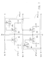
- FIG. 5 shows a diagram of the time domain multiplex driving circuit according to a first embodiment of the present invention.
- the pixel LP(m,n) is set on the left side of the data line D n and the pixel RP(m,n) is set on the right side of the data line D n , as shown in FIG. 5 .
- the switching device of the pixel RP(m,n) includes a switch M 2 which is used for selectively transmitting the data signal loaded on the data line D n to the pixel RP(m,n).
- the switching device of the pixel LP(m,n) includes two switches M 11 and M 12 which are used for selectively transmitting the data signal on the data line D n to the pixel LP(m,n). It should be noticed that all the switches can be thin film transistors and the pixel with two switches(i.e. LP(m,n)) can be set on the right side of the data line and the pixel with only one switch (i.e. RP(m,n)) can then be set on the left side of the data line.
- the switching device of the pixel RP(m,n) includes a thin film transistor M 2 .
- the gate electrode of the thin film transistor M 2 (g 2 ) is coupled to the scan line S m and the source electrode of the thin film transistor M 2 (s 2 ) is coupled to the data line D n respectively.
- the switching device of the pixel LP(m,n) is different from that of the pixel RP(m,n).
- the switching device of the pixel LP(m,n) includes two thin film transistors M 11 and M 12 .
- the gate electrode of the thin film transistor M 11 (g 11 ) is coupled to the scan line S m+1 and the source electrode of the thin film transistor M 11 (s 11 ) is coupled to the scan line S m .
- the source electrode (s 12 ) and the gate electrode (g 12 ) of the thin film transistor M 12 are coupled to the data line D n and the drain electrode of the thin film transistor M 11 (d 11 ) respectively, as shown in FIG. 5 .
- the switching device of the time domain multiplex driving circuit of the present invention is different from that of the conventional time domain multiplex driving circuit.
- pixel LP(m,n) shown in FIG. 3 and the pixel LP(m,n) shown in FIG. 5 for example.
- Both the pixel LP(m,n) shown in FIG. 3 and the pixel LP(m,n) shown in FIG. 5 include two corresponding thin film transistors.
- the gate electrode of the thin film transistors M 11 (g 11 ) and M 12 (g 12 ) are coupled to the scan lines S m+1 and S m respectively. Therefore, the thin film transistors M 11 can be turned ON by enabling scan line S m+1 directly and the thin film transistor M 12 can be turned ON by enabling scan line S m directly.
- the ON and OFF status of the thin film transistor cannot be controlled by the other thin film transistor.
- the gate electrode of the thin film transistor M 12 (g 12 ) is coupled to the drain electrode of the thin film transistor M 11 (d 11 ). Therefore, the ON and OFF status of the thin film transistor M 12 can be controlled by the thin film transistor M 11 .
- the thin film transistor M 12 cannot be turned ON unless the thin film transistor M 11 is turned ON.
- FIG. 6 shows the timing chart of the scan signals of the scan line S m , S m+1 , and S m+2 and the ON and OFF status of the corresponding pixels LP(m,n), RP(m,n), LP(m+1,n), and RP(m+1,n) shown in FIG. 5 .
- the time domain multiplex driving method executed by the above-described time domain multiplex driving circuit is used for driving each pixel row in turn.
- the time domain multiplex driving method includes two scanning procedures. The first scanning procedure is used for turning ON the pixels that are respectively associated with two thin film transistors in the pixel row and then applying the corresponding data signals to these pixels respectively. The second scanning procedure is used for turning ON the pixels that are respectively associated with only one thin film transistor in the pixel row and then inputting the corresponding data signals into the pixels respectively.
- the first scanning procedure is executed so that the scan line S m and S m+1 are enabled.
- the scan line S m+1 is coupled to the gate electrode of the thin film transistor M 11 (g 11 ).
- the thin film transistor M 11 can be turned ON in the time period T 1 . Since the thin film transistor M 11 is turned ON, the scan line S m is electrically coupled to the gate electrode of the thin film transistor M 12 (g 12 ).
- the scan signal of the scan line S m can be transmitted through the source electrode (s 11 ) and the drain electrode (d 11 ) of the thin film transistor M 11 to the gate electrode of the thin film transistor M 12 (g 12 ). Therefore, the thin film transistor M 12 can be turned ON. It should be noticed that the thin film transistor M 12 cannot be turned ON unless the thin film transistor M 11 is turned ON. In this manner, the corresponding data signal on the data line D n is inputted to the pixel LP(m,n) in the time period T 1 . After the data signals are inputted into the pixel LP(m,n), the scan line S m is disabled. The thin film transistor M 11 can be turned OFF after the scan line S m is disabled. Then, the scan line S m+1 is disabled. The thin film transistor M 12 can be turned OFF after the scan line S m+1 is disabled. In this manner, the first scanning procedure is accomplished.
- the second scanning procedure is executed, wherein the scan line S m is enabled again.
- the thin film transistor M 2 is turned ON after the scan line S m is enabled.
- the corresponding data signal of the pixel RP(m,n) is inputted to the pixel RP(m,n) through the data line D n in the time period T 2 .
- the scan line S m is to be disabled. In this manner, the second scanning procedure of the time domain multiplex driving method is accomplished.
- the thin film transistor of the pixel RP(m,n), M 2 can be turned ON as well as the thin film transistor M 11 and M 12 in the pixel LP(m,n).
- the data signal corresponded to the pixel LP(m,n) is inputted to the pixel RP(m,n) as well.
- the thin film transistor of the pixel RP(m,n), M 2 can still be turned ON and the data signal corresponded to the pixel RP(m,n) is inputted to the pixel RP(m,n) through the data line D n .
- the thin film transistor M 12 of the pixel LP(m,n) cannot be turned ON since thin film transistor M 11 of the pixel LP(m,n) is turned OFF, as shown in FIG. 6 . Therefore, the data signal corresponded to the pixel RP(m,n) cannot be inputted to the pixel LP(m,n) in the time period T 2 . In this manner, after the first and the second scanning procedure are accomplished, the data signals corresponded to the pixels LP(m,n) and RP(m,n) are inputted to the corresponding pixels respectively.
- the time domain multiplex driving circuit of the present invention has the following advantages. First, it takes less driving time to input all data signals into the corresponding pixels. Take the pixel LP(m,n) shown in FIG. 5 for example. Although the switching device of the pixel LP(m,n) includes two thin film transistors M 11 and M 12 , the corresponding data signal can be inputted to the pixel LP(m,n) through the thin film transistor M 12 only and then the pixel LP(m,n) substantially has an equivalent resistance equal to R o . Compared with the pixel LP(m,n) shown in FIG. 3, the equivalent resistance of the pixel LP(m,n) shown in FIG. 5 is R o instead of 2R o . Therefore, it takes less driving time to input all data signals into the corresponding pixels.
- the degree of the feed-through effect and the difference between the output voltage and the input voltage of the thin film transistor is reduced.
- the switching device of the pixel LP(m,n) includes two thin film transistors M 11 and M 12 , the corresponding data signal can be inputted to the pixel LP(m,n) through the thin film transistor M 12 only.
- the equivalent capacitance of the pixel LP(m,n) of the embodiment is much smaller than that of the conventional time domain multiplex driving circuit. Therefore, the degree of the feed-through effect and the difference between the output voltage and the input voltage of the thin film transistor can be decreased.
- the switching device of each pixel in the same pixel column includes two thin film transistor and the switching device of each pixel in the adjacent column includes only one transistor, as shown in FIG. 5, the luminance of each pixel column can be more similar to that of the adjacent pixel column when the data signals of the same magnitude are inputted to these pixel columns. In this way, the odd-even line problem becomes insignificant.
- the display performance of the display panel can be improved.
- FIG. 7 shows a diagram of the time domain multiplex driving circuit according to a second embodiment of the present invention.
- the pixel LP(m,n) is set on the left side of the data line D n and the pixel RP(m,n) is set on the right side of the data line D n , as shown in FIG. 7 .
- the switching device of the pixel LP(m,n) includes a switch M 1 which is used for selectively transmitting the data signal on the data line D n to the pixel LP(m,n).
- the switching device of the pixel RP(m,n) includes two switches M 21 and M 22 which are used for selectively transmitting the data signal on the data line D n to the pixel RP(m,n). It should be noticed that all the switches can be thin film transistors and the pixel with two switches can be set on the left side of the data line and the pixel with only one switch can then be set on the right side of the data line.
- the switching device of the pixel LP(m,n) includes a thin film transistor M 1 .
- the gate electrode of the thin film transistor M 1 (g 1 ) is coupled to the scan line S m and the source electrode of the thin film transistor M 1 (s 1 ) is coupled to the data line D n .
- the switching device of the pixel RP(m,n) is different from that of the pixel LP(m,n).
- the switching device of the pixel RP(m,n) includes two thin film transistors M 21 and M 22 .
- the gate electrode of the thin film transistor M 21 (g 21 ) is coupled to the scan line S m
- the source electrode of the thin film transistor M 21 (s 21 ) is coupled to the scan line S m+1 .
- the source electrode of the thin film transistor M 22 (s 22 ) is coupled to the data line D n and the gate electrode of the thin film transistor M 22 (g 22 ) is coupled to the drain electrode of the thin film transistor M 21 (d 21 ), as shown in FIG. 7 .
- the coupling relation between the thin film transistors M 21 and M 22 of the pixel RP(m,n) shown in FIG. 7 is different than that of the thin film transistors M 11 and M 12 of the pixel LP(m,n) shown in FIG. 5 .
- the feature of the time domain multiplex driving circuit disclosed in the second embodiment is similar to that of the first embodiment of the present invention. Take the pixel RP(m,n) shown in FIG. 7 for example.
- the gate electrode of the thin film transistor M 22 (g 22 ) is coupled to the drain electrode of the thin film transistor M 21 (d 21 ). Therefore, the ON and OFF status of the thin film transistor M 22 can be controlled by the thin film transistor M 21 .
- the thin film transistor M 22 cannot be turned ON unless the thin film transistor M 21 is turned ON.
- FIG. 8 shows a timing chart of the scan signals of the scan line S m , S m+1 , and S m+2 and the ON and OFF status of the corresponding pixels LP(m,n), RP(m,n), LP(m+1,n), and RP(m+1,n) shown in FIG. 7 .
- the time domain multiplex driving method executed by the above-described time domain multiplex driving circuit includes two scanning procedures.
- the first scanning procedure is used for turning ON each pixel with two thin film transistors in the pixel row and then inputting the corresponding data signals into these pixels respectively.
- the second scanning procedure is used for turning ON each pixel with only one thin film transistor in the pixel row and then inputting the corresponding data signals into the pixels respectively
- the first scanning procedure is executed, and the scan line S m and S m+1 are enabled.
- the scan line S m is coupled to the gate electrode of the thin film transistor M 21 (g 21 ).
- the thin film transistor M 21 can be turned ON.
- the scan line S m+ 1 is electrically coupled to the gate electrode of the thin film transistor M 22 (g 22 ). Therefore, the corresponding scan signal of the scan line S m+1 can be transmitted to the gate electrode of the thin film transistor M 22 through the source electrode (s 21 ) and the drain electrode (d 21 ) of the thin film transistor M 21 .
- the thin film transistor M 22 can be turned ON. It should be noticed that the thin film transistor M 22 cannot be turned ON unless the thin film transistor M 21 is turned ON. In this manner, the data signal corresponded to the pixel RP(m,n) can be inputted to the pixel RP(m,n) through the data line D n in the time period T 1 . After inputting the data signals into the pixel LP(m,n), the scan line S m+1 will be disabled. The thin film transistor M 22 can be turned OFF after the scan line S m+1 is disabled. Besides, the scan line S m is still enabled in the end of the time period T 1 . In this manner, the first scanning procedure is accomplished.
- the second scanning procedure is executed. Since the scan line S m is still enabled and the gate electrode of the thin film transistor M 1 (g 1 ) is coupled to the scan line S m , the thin film transistor M 1 can be turned ON. The corresponding data signal can be inputted to the pixel LP(m,n) through the data line D n in the time period T 2 . After the data signal is inputed to the pixel LP(m,n), the scan line S m can be disabled. In this manner, the second scanning procedure of the time domain multiplex driving method is accomplished.
- the thin film transistor of the pixel LP(m,n), M 1 as well as the thin film transistor M 21 and M 22 in the pixel RP(m,n) can be turned ON.
- the data signal corresponded to the pixel RP(m,n) is inputted to the pixel LP(m,n) in the time period T 1 .
- the thin film transistor of the pixel LP(m,n), M 1 is still turned ON and the data signal corresponded to the pixel LP(m,n) is inputted to the pixel LP(m,n) through the data line D n in this time period T 2 .
- the thin film transistor M 22 of the pixel RP(m,n) cannot be turned ON since thin film transistor M 21 of the pixel RP(m,n) has been turned OFF, as shown in FIG. 8 . Therefore, the data signal corresponded to the pixel LP(m,n) cannot be to the pixel RP(m,n) in the time period T 2 . In this manner, after the first and the second scanning procedures are accomplished, the data signals corresponded to the pixels LP(m,n) and RP(m,n) are inputted to the corresponding pixels respectively.
- the advantages of the time domain multiplex driving circuit disclosed in the second embodiment are similar to that of the first embodiment of the present invention.
- Third, the difference between the luminance of the pixel LP(m,n) and that of the pixel RP(m,n) is insignificant when the data signals of the same magnitude are fed to the pixels LP(m,n) and RP(m,n), the odd-even line problem cannot happen, and the display performance of the display panel can be improved.
- the pixels coupled to both the same scan line and the same data line form a pixel group.
- the pixels LP(m,n) and RP(m,n) shown in FIG. 7 are coupled to both the scan line S m and the data line D n . These two pixels can be viewed as a pixel group P(m,n).
- the pixels LP(m+1,n) and RP(m+1,n) forms a pixel group P(m+1,n).
- the switching device of the pixel LP(m,n) is the same as that of the pixel RP(m+1,n)
- the switching device of the pixel RP(m,n) is the same as that of the pixel LP(m+1,n).
- FIG. 9 is a first mirror-image configuration of a time domain multiplex driving circuit according to the present invention.
- each pixel group coupled to one data line is the horizontal mirror image of the adjacent pixel group coupled to the same data line.
- FIG. 10 shows a second mirror-image configuration of a time domain multiplex driving circuit according to the present invention.
- the pixel group P(m,n) is the same as the pixel group P(m+1,n+1) while the pixel group P(m,n+1) is the same as the pixel group P(m+1,n). Therefore, all pixels of the same pixel column are not the same and all pixels of the same pixel row are not the same, either. In this manner, the odd-even line problem can be further improved.
- the best mode of the display apparatus with the time domain multiplex driving circuit in accordance with the invention has the following advantages.
- Third, the luminance of the pixel with two thin film transistors is similar to that of the pixel with only one thin film transistor when the data signals of the same magnitude are inputted to these two kinds of pixels. Fourth, the odd-even line problem can be improved. If the pixels are set in the mirror image form, the odd-even problem can be further improved.
Landscapes
- Engineering & Computer Science (AREA)
- Chemical & Material Sciences (AREA)
- Crystallography & Structural Chemistry (AREA)
- Physics & Mathematics (AREA)
- Computer Hardware Design (AREA)
- General Physics & Mathematics (AREA)
- Theoretical Computer Science (AREA)
- Control Of Indicators Other Than Cathode Ray Tubes (AREA)
- Liquid Crystal Display Device Control (AREA)
Abstract
Description
Claims (26)
Applications Claiming Priority (3)
| Application Number | Priority Date | Filing Date | Title |
|---|---|---|---|
| TW90119364A | 2001-08-09 | ||
| TW090119364A TW523724B (en) | 2001-08-09 | 2001-08-09 | Display panel with time domain multiplex driving circuit |
| TW90119364 | 2001-08-09 |
Publications (2)
| Publication Number | Publication Date |
|---|---|
| US20030030609A1 US20030030609A1 (en) | 2003-02-13 |
| US6825822B2 true US6825822B2 (en) | 2004-11-30 |
Family
ID=21678996
Family Applications (1)
| Application Number | Title | Priority Date | Filing Date |
|---|---|---|---|
| US10/212,124 Expired - Lifetime US6825822B2 (en) | 2001-08-09 | 2002-08-06 | Display apparatus with a time domain multiplex driving circuit |
Country Status (2)
| Country | Link |
|---|---|
| US (1) | US6825822B2 (en) |
| TW (1) | TW523724B (en) |
Cited By (8)
| Publication number | Priority date | Publication date | Assignee | Title |
|---|---|---|---|---|
| US20050041006A1 (en) * | 2003-08-21 | 2005-02-24 | Lee Jae Kyun | Liquid crystal display apparatus and driving method thereof |
| US20050052400A1 (en) * | 2002-12-31 | 2005-03-10 | Lg. Philips Lcd Co., Ltd. | Liquid crystal display device |
| US20050122304A1 (en) * | 2003-12-08 | 2005-06-09 | Lg Philips Lcd Co., Ltd. | Liquid crystal display device and driving method thereof |
| US20070159444A1 (en) * | 2006-01-06 | 2007-07-12 | Au Optronics Corporation | Display Array of Display Panel |
| US20070222736A1 (en) * | 2006-03-23 | 2007-09-27 | Au Optronics Corp. | Method of driving liquid crystal display panel |
| US20100045631A1 (en) * | 2008-08-21 | 2010-02-25 | Wu-Min Chen | Matrix sensing apparatus |
| US20110304655A1 (en) * | 2010-06-10 | 2011-12-15 | Casio Computer Co., Ltd | Display device |
| US20140118238A1 (en) * | 2012-10-26 | 2014-05-01 | Shenzhen China Star Optoelectronics Technology Co. Ltd. | Liquid crystal display drive circuit |
Families Citing this family (7)
| Publication number | Priority date | Publication date | Assignee | Title |
|---|---|---|---|---|
| JP4390469B2 (en) * | 2003-03-26 | 2009-12-24 | Necエレクトロニクス株式会社 | Image display device, signal line drive circuit used in image display device, and drive method |
| FR2866465A1 (en) * | 2004-02-18 | 2005-08-19 | Thomson Licensing Sa | Front/rear projector type image display device stores specific and common values associated with video data to be displayed by each liquid crystal element of valve and group of at least two adjacent elements respectively |
| US20060044241A1 (en) * | 2004-08-31 | 2006-03-02 | Vast View Technology Inc. | Driving device for quickly changing the gray level of the liquid crystal display and its driving method |
| KR100827453B1 (en) * | 2004-12-29 | 2008-05-07 | 엘지디스플레이 주식회사 | Electroluminescent display device and driving method thereof |
| KR100665943B1 (en) * | 2005-06-30 | 2007-01-09 | 엘지.필립스 엘시디 주식회사 | Organic electroluminescent display device and driving method |
| JP4775407B2 (en) * | 2008-05-30 | 2011-09-21 | カシオ計算機株式会社 | Display device |
| TWI385454B (en) * | 2008-09-15 | 2013-02-11 | Chimei Innolux Corp | Liquid crystal display panel |
Citations (10)
| Publication number | Priority date | Publication date | Assignee | Title |
|---|---|---|---|---|
| US4781438A (en) * | 1987-01-28 | 1988-11-01 | Nec Corporation | Active-matrix liquid crystal color display panel having a triangular pixel arrangement |
| US5453857A (en) * | 1993-03-22 | 1995-09-26 | Matsushita Electric Industrial Co., Ltd. | Liquid crystal display with two transistors per pixel driven at opposite polarities |
| US5844535A (en) * | 1995-06-23 | 1998-12-01 | Kabushiki Kaisha Toshiba | Liquid crystal display in which each pixel is selected by the combination of first and second address lines |
| US20010017610A1 (en) * | 1999-12-28 | 2001-08-30 | Tokuro Ozawa | Electro-optical device, driving circuit and driving method of electro-optical device, and electronic apparatus |
| US20010024186A1 (en) * | 1997-09-29 | 2001-09-27 | Sarnoff Corporation | Active matrix light emitting diode pixel structure and concomitant method |
| US20020005825A1 (en) * | 2000-07-15 | 2002-01-17 | Lee Han Sang | Electro-luminescence panel |
| US20020044124A1 (en) * | 2000-06-05 | 2002-04-18 | Shunpei Yamazaki | Display panel, display panel inspection method, and display panel manufacturing method |
| US6417825B1 (en) * | 1998-09-29 | 2002-07-09 | Sarnoff Corporation | Analog active matrix emissive display |
| US20020149553A1 (en) * | 2000-03-31 | 2002-10-17 | Takatoshi Tsujimura | Display device having driving elements, and driving method thereof |
| US20030160751A1 (en) * | 1999-09-13 | 2003-08-28 | Yasuyuki Kudo | Liquid crystal display apparatus and liquid crystal display driving method |
-
2001
- 2001-08-09 TW TW090119364A patent/TW523724B/en not_active IP Right Cessation
-
2002
- 2002-08-06 US US10/212,124 patent/US6825822B2/en not_active Expired - Lifetime
Patent Citations (10)
| Publication number | Priority date | Publication date | Assignee | Title |
|---|---|---|---|---|
| US4781438A (en) * | 1987-01-28 | 1988-11-01 | Nec Corporation | Active-matrix liquid crystal color display panel having a triangular pixel arrangement |
| US5453857A (en) * | 1993-03-22 | 1995-09-26 | Matsushita Electric Industrial Co., Ltd. | Liquid crystal display with two transistors per pixel driven at opposite polarities |
| US5844535A (en) * | 1995-06-23 | 1998-12-01 | Kabushiki Kaisha Toshiba | Liquid crystal display in which each pixel is selected by the combination of first and second address lines |
| US20010024186A1 (en) * | 1997-09-29 | 2001-09-27 | Sarnoff Corporation | Active matrix light emitting diode pixel structure and concomitant method |
| US6417825B1 (en) * | 1998-09-29 | 2002-07-09 | Sarnoff Corporation | Analog active matrix emissive display |
| US20030160751A1 (en) * | 1999-09-13 | 2003-08-28 | Yasuyuki Kudo | Liquid crystal display apparatus and liquid crystal display driving method |
| US20010017610A1 (en) * | 1999-12-28 | 2001-08-30 | Tokuro Ozawa | Electro-optical device, driving circuit and driving method of electro-optical device, and electronic apparatus |
| US20020149553A1 (en) * | 2000-03-31 | 2002-10-17 | Takatoshi Tsujimura | Display device having driving elements, and driving method thereof |
| US20020044124A1 (en) * | 2000-06-05 | 2002-04-18 | Shunpei Yamazaki | Display panel, display panel inspection method, and display panel manufacturing method |
| US20020005825A1 (en) * | 2000-07-15 | 2002-01-17 | Lee Han Sang | Electro-luminescence panel |
Cited By (17)
| Publication number | Priority date | Publication date | Assignee | Title |
|---|---|---|---|---|
| US7256759B2 (en) * | 2002-12-31 | 2007-08-14 | Lg.Philips Lcd Co., Ltd. | Liquid crystal display device |
| US20050052400A1 (en) * | 2002-12-31 | 2005-03-10 | Lg. Philips Lcd Co., Ltd. | Liquid crystal display device |
| US20050041006A1 (en) * | 2003-08-21 | 2005-02-24 | Lee Jae Kyun | Liquid crystal display apparatus and driving method thereof |
| US7425942B2 (en) * | 2003-08-21 | 2008-09-16 | Lg Display Co., Ltd. | Liquid crystal display apparatus and driving method thereof |
| US20090195532A1 (en) * | 2003-12-08 | 2009-08-06 | Lg Display Co., Ltd. | Liquid crystal device and driving method thereof |
| US7535445B2 (en) * | 2003-12-08 | 2009-05-19 | Lg. Display Co., Ltd. | Liquid crystal display device and driving method thereof |
| US20050122304A1 (en) * | 2003-12-08 | 2005-06-09 | Lg Philips Lcd Co., Ltd. | Liquid crystal display device and driving method thereof |
| US8120559B2 (en) | 2003-12-08 | 2012-02-21 | Lg Display Co., Ltd. | Liquid crystal device and driving method thereof |
| US20070159444A1 (en) * | 2006-01-06 | 2007-07-12 | Au Optronics Corporation | Display Array of Display Panel |
| US20070222736A1 (en) * | 2006-03-23 | 2007-09-27 | Au Optronics Corp. | Method of driving liquid crystal display panel |
| US7714823B2 (en) | 2006-03-23 | 2010-05-11 | Au Optronics Corp. | Method of driving liquid crystal display panel |
| US20100045631A1 (en) * | 2008-08-21 | 2010-02-25 | Wu-Min Chen | Matrix sensing apparatus |
| US8154528B2 (en) * | 2008-08-21 | 2012-04-10 | Au Optronics Corp. | Matrix sensing apparatus |
| US20110304655A1 (en) * | 2010-06-10 | 2011-12-15 | Casio Computer Co., Ltd | Display device |
| US8928702B2 (en) * | 2010-06-10 | 2015-01-06 | Casio Computer Co., Ltd. | Display device having a reduced number of signal lines |
| US20140118238A1 (en) * | 2012-10-26 | 2014-05-01 | Shenzhen China Star Optoelectronics Technology Co. Ltd. | Liquid crystal display drive circuit |
| US9024853B2 (en) * | 2012-10-26 | 2015-05-05 | Shenzhen China Star Optoelectronics Technology Co., Ltd | Liquid crystal display drive circuit |
Also Published As
| Publication number | Publication date |
|---|---|
| TW523724B (en) | 2003-03-11 |
| US20030030609A1 (en) | 2003-02-13 |
Similar Documents
| Publication | Publication Date | Title |
|---|---|---|
| US6982690B2 (en) | Display apparatus with a driving circuit in which every three adjacent pixels are coupled to the same data line | |
| US6999053B2 (en) | Display apparatus with a time domain multiplex driving circuit | |
| US8405593B2 (en) | Liquid crystal device with multi-dot inversion | |
| US7796108B2 (en) | Liquid crystal display device, active matrix type liquid crystal display device, and method of driving the same | |
| US6825822B2 (en) | Display apparatus with a time domain multiplex driving circuit | |
| KR100228282B1 (en) | Liquid crystal display | |
| US5877737A (en) | Wide viewing angle driving circuit and method for liquid crystal display | |
| US11056057B2 (en) | Array substrate, display apparatus, and method of driving array substrate | |
| US7071928B2 (en) | Liquid crystal display device having quad type color filters | |
| EP0825584A2 (en) | Driving method and circuit for an array of display cells or light valves | |
| US7400306B2 (en) | Driving method for dual panel display | |
| US6859195B2 (en) | Display device driven with dual transistors | |
| US6873378B2 (en) | Liquid crystal display panel | |
| US10262607B2 (en) | Driving circuits of liquid crystal panels and liquid crystal displays | |
| US20040075632A1 (en) | Liquid crystal display panel and driving method thereof | |
| US7342566B2 (en) | Liquid crystal display device and driving method thereof | |
| US20060279513A1 (en) | Apparatus and method for driving gate lines in a flat panel display (FPD) | |
| US7755591B2 (en) | Display panel and device utilizing the same and pixel structure | |
| US8319719B2 (en) | Liquid crystal display device | |
| US7274359B2 (en) | Display device and circuit board therefor including interconnection for signal transmission | |
| US20040252098A1 (en) | Liquid crystal display panel | |
| US7420537B2 (en) | Liquid crystal display and dummy loading device thereof | |
| KR100266217B1 (en) | Flicker prevention liquid crystal display device | |
| KR100686503B1 (en) | Electro-optical devices and electronics | |
| US20070171165A1 (en) | Devices and methods for controlling timing sequences for displays of such devices |
Legal Events
| Date | Code | Title | Description |
|---|---|---|---|
| AS | Assignment |
Owner name: CHI MEI OPTOELECTRONICS CORP., TAIWAN Free format text: ASSIGNMENT OF ASSIGNORS INTEREST;ASSIGNOR:LEE, HSIN-TA;REEL/FRAME:013173/0201 Effective date: 20020722 |
|
| STCF | Information on status: patent grant |
Free format text: PATENTED CASE |
|
| FPAY | Fee payment |
Year of fee payment: 4 |
|
| AS | Assignment |
Owner name: CHIMEI INNOLUX CORPORATION,TAIWAN Free format text: MERGER;ASSIGNOR:CHI MEI OPTOELECTRONICS CORP.;REEL/FRAME:024329/0699 Effective date: 20100318 |
|
| FPAY | Fee payment |
Year of fee payment: 8 |
|
| AS | Assignment |
Owner name: INNOLUX CORPORATION, TAIWAN Free format text: CHANGE OF NAME;ASSIGNOR:CHIMEI INNOLUX CORPORATION;REEL/FRAME:032604/0487 Effective date: 20121219 |
|
| FPAY | Fee payment |
Year of fee payment: 12 |