US8081148B2 - Display device - Google Patents
Display device Download PDFInfo
- Publication number
- US8081148B2 US8081148B2 US11/936,116 US93611607A US8081148B2 US 8081148 B2 US8081148 B2 US 8081148B2 US 93611607 A US93611607 A US 93611607A US 8081148 B2 US8081148 B2 US 8081148B2
- Authority
- US
- United States
- Prior art keywords
- circuit
- video
- protecting
- lines
- display device
- Prior art date
- Legal status (The legal status is an assumption and is not a legal conclusion. Google has not performed a legal analysis and makes no representation as to the accuracy of the status listed.)
- Expired - Fee Related, expires
Links
- 230000001681 protective effect Effects 0.000 claims abstract description 110
- 230000002093 peripheral effect Effects 0.000 claims abstract description 50
- 239000000758 substrate Substances 0.000 claims abstract description 49
- 238000007689 inspection Methods 0.000 claims description 20
- 230000015556 catabolic process Effects 0.000 abstract description 10
- 230000005611 electricity Effects 0.000 abstract description 10
- 230000003068 static effect Effects 0.000 abstract description 10
- 239000004973 liquid crystal related substance Substances 0.000 description 34
- 239000010409 thin film Substances 0.000 description 18
- 239000004065 semiconductor Substances 0.000 description 8
- 102100031491 Arylsulfatase B Human genes 0.000 description 5
- 101000923070 Homo sapiens Arylsulfatase B Proteins 0.000 description 5
- 239000000463 material Substances 0.000 description 4
- 238000004088 simulation Methods 0.000 description 4
- 239000003566 sealing material Substances 0.000 description 3
- 238000010586 diagram Methods 0.000 description 2
- 238000004519 manufacturing process Methods 0.000 description 2
- 239000011159 matrix material Substances 0.000 description 2
- 238000000034 method Methods 0.000 description 2
- 102100033887 Arylsulfatase D Human genes 0.000 description 1
- 101000925559 Homo sapiens Arylsulfatase D Proteins 0.000 description 1
- 229910021417 amorphous silicon Inorganic materials 0.000 description 1
- 230000007547 defect Effects 0.000 description 1
- 230000000694 effects Effects 0.000 description 1
- 239000010408 film Substances 0.000 description 1
- 239000011521 glass Substances 0.000 description 1
- 238000009413 insulation Methods 0.000 description 1
- 238000012986 modification Methods 0.000 description 1
- 230000004048 modification Effects 0.000 description 1
- 239000011295 pitch Substances 0.000 description 1
- 229910021420 polycrystalline silicon Inorganic materials 0.000 description 1
- 229920005591 polysilicon Polymers 0.000 description 1
Images


Classifications
-
- G—PHYSICS
- G09—EDUCATION; CRYPTOGRAPHY; DISPLAY; ADVERTISING; SEALS
- G09G—ARRANGEMENTS OR CIRCUITS FOR CONTROL OF INDICATING DEVICES USING STATIC MEANS TO PRESENT VARIABLE INFORMATION
- G09G3/00—Control arrangements or circuits, of interest only in connection with visual indicators other than cathode-ray tubes
- G09G3/20—Control arrangements or circuits, of interest only in connection with visual indicators other than cathode-ray tubes for presentation of an assembly of a number of characters, e.g. a page, by composing the assembly by combination of individual elements arranged in a matrix no fixed position being assigned to or needed to be assigned to the individual characters or partial characters
-
- G—PHYSICS
- G02—OPTICS
- G02F—OPTICAL DEVICES OR ARRANGEMENTS FOR THE CONTROL OF LIGHT BY MODIFICATION OF THE OPTICAL PROPERTIES OF THE MEDIA OF THE ELEMENTS INVOLVED THEREIN; NON-LINEAR OPTICS; FREQUENCY-CHANGING OF LIGHT; OPTICAL LOGIC ELEMENTS; OPTICAL ANALOGUE/DIGITAL CONVERTERS
- G02F1/00—Devices or arrangements for the control of the intensity, colour, phase, polarisation or direction of light arriving from an independent light source, e.g. switching, gating or modulating; Non-linear optics
- G02F1/01—Devices or arrangements for the control of the intensity, colour, phase, polarisation or direction of light arriving from an independent light source, e.g. switching, gating or modulating; Non-linear optics for the control of the intensity, phase, polarisation or colour
- G02F1/13—Devices or arrangements for the control of the intensity, colour, phase, polarisation or direction of light arriving from an independent light source, e.g. switching, gating or modulating; Non-linear optics for the control of the intensity, phase, polarisation or colour based on liquid crystals, e.g. single liquid crystal display cells
- G02F1/133—Constructional arrangements; Operation of liquid crystal cells; Circuit arrangements
- G02F1/136—Liquid crystal cells structurally associated with a semi-conducting layer or substrate, e.g. cells forming part of an integrated circuit
- G02F1/1362—Active matrix addressed cells
- G02F1/136204—Arrangements to prevent high voltage or static electricity failures
-
- G—PHYSICS
- G02—OPTICS
- G02F—OPTICAL DEVICES OR ARRANGEMENTS FOR THE CONTROL OF LIGHT BY MODIFICATION OF THE OPTICAL PROPERTIES OF THE MEDIA OF THE ELEMENTS INVOLVED THEREIN; NON-LINEAR OPTICS; FREQUENCY-CHANGING OF LIGHT; OPTICAL LOGIC ELEMENTS; OPTICAL ANALOGUE/DIGITAL CONVERTERS
- G02F2202/00—Materials and properties
- G02F2202/22—Antistatic materials or arrangements
-
- G—PHYSICS
- G09—EDUCATION; CRYPTOGRAPHY; DISPLAY; ADVERTISING; SEALS
- G09G—ARRANGEMENTS OR CIRCUITS FOR CONTROL OF INDICATING DEVICES USING STATIC MEANS TO PRESENT VARIABLE INFORMATION
- G09G2300/00—Aspects of the constitution of display devices
- G09G2300/08—Active matrix structure, i.e. with use of active elements, inclusive of non-linear two terminal elements, in the pixels together with light emitting or modulating elements
-
- G—PHYSICS
- G09—EDUCATION; CRYPTOGRAPHY; DISPLAY; ADVERTISING; SEALS
- G09G—ARRANGEMENTS OR CIRCUITS FOR CONTROL OF INDICATING DEVICES USING STATIC MEANS TO PRESENT VARIABLE INFORMATION
- G09G2330/00—Aspects of power supply; Aspects of display protection and defect management
- G09G2330/06—Handling electromagnetic interferences [EMI], covering emitted as well as received electromagnetic radiation
-
- G—PHYSICS
- G09—EDUCATION; CRYPTOGRAPHY; DISPLAY; ADVERTISING; SEALS
- G09G—ARRANGEMENTS OR CIRCUITS FOR CONTROL OF INDICATING DEVICES USING STATIC MEANS TO PRESENT VARIABLE INFORMATION
- G09G3/00—Control arrangements or circuits, of interest only in connection with visual indicators other than cathode-ray tubes
- G09G3/20—Control arrangements or circuits, of interest only in connection with visual indicators other than cathode-ray tubes for presentation of an assembly of a number of characters, e.g. a page, by composing the assembly by combination of individual elements arranged in a matrix no fixed position being assigned to or needed to be assigned to the individual characters or partial characters
- G09G3/34—Control arrangements or circuits, of interest only in connection with visual indicators other than cathode-ray tubes for presentation of an assembly of a number of characters, e.g. a page, by composing the assembly by combination of individual elements arranged in a matrix no fixed position being assigned to or needed to be assigned to the individual characters or partial characters by control of light from an independent source
- G09G3/36—Control arrangements or circuits, of interest only in connection with visual indicators other than cathode-ray tubes for presentation of an assembly of a number of characters, e.g. a page, by composing the assembly by combination of individual elements arranged in a matrix no fixed position being assigned to or needed to be assigned to the individual characters or partial characters by control of light from an independent source using liquid crystals
- G09G3/3611—Control of matrices with row and column drivers
- G09G3/3648—Control of matrices with row and column drivers using an active matrix
Definitions
- the present invention relates to a display device, and more particularly to a display device which arranges a protective element (diode element) for electrostatic protection in the inside of a display panel.
- a TFT-type liquid crystal display module which uses thin film transistors as active elements can display a high-definition image and hence, the liquid crystal display module has been used as display devices of television receiver sets, displays of personal computers and the like. Particularly, a miniaturized TFT-type liquid crystal display device has been popularly used as a display part of a mobile phone.
- a thin film transistor which is turned on in response to a scanning signal from the scanning line and a pixel electrode to which the video signal from the video line is transmitted via the above-mentioned thin film transistor are formed thus constituting a so-called pixel.
- a protective circuit is formed on one of substrates which constitute the liquid crystal display panel on an outer portion of the substrate.
- the thin film transistor which uses polysilicon as a material of a semiconductor layer exhibits, compared to a thin film transistor which uses amorphous silicon as a material of a semiconductor layer, high performance as an MOS transistor but a low breakdown voltage and hence, the thin film transistor which uses the polysilicon-made semiconductor layer requires protection against electrostatic breakdown attributed to static electricity.
- symbol VDSC indicates a video voltage selection circuit
- symbol VSCA indicates a vertical scanning circuit
- symbol TEST indicates an inspection circuit
- symbol SECL indicates a cell cutting line.
- the protective circuit As mentioned previously, to prevent electrostatic breakdown attributed to static electricity, conventionally, on one of substrates which constitutes the liquid crystal display panel, the protective circuit (HOGC) is formed outside the cell cutting line (SECL) shown in FIG. 8 .
- the present invention has been made to overcome the above-mentioned drawback of the related art, and it is an object of the present invention to provide a technique, in a display device, which can prevent electrostatic breakdown attributed to static electricity even in and after a cell cutting step.
- the electrostatic protective circuit for protecting the pixel part is connected between the plurality of video lines, and an electrostatic protective circuit for protecting a peripheral circuit is connected between at least one video line and a reference voltage line to which a reference voltage is applied.
- a display device which includes a substrate, a plurality of pixels which is formed in a pixel part, a plurality of video lines which applies video voltages to the plurality of pixels, and a video voltage selection circuit which selects the video voltages to be inputted to the pixels and applies the selected video voltages to the predetermined video lines among the plurality of video lines, an electrostatic protective circuit for protecting a pixel part is connected to the plurality of video voltage inputting lines which inputs the video voltages to the video voltage selection circuit, and an electrostatic protective circuit for protecting a peripheral circuit is connected to the lines other than the video voltage inputting lines which is connected to the video voltage selection circuit.
- the electrostatic protective circuit for protecting the pixel part is connected between the plurality of video voltage inputting lines
- the electrostatic protective circuit for protecting the peripheral circuit is connected between the at least one video voltage inputting line and the line other than the at least one video voltage inputting line, between the plurality of lines other than the video voltage inputting lines, and between the line other than the at least one video voltage inputting line and a reference voltage line to which a reference voltage is applied.
- the display device includes a plurality of scanning lines which applies scanning voltages to the plurality of pixels, and the electrostatic protective circuit for protecting the pixel part is connected between the plurality of scanning lines and the reference voltage line to which the reference voltage is applied.
- the display device includes a scanning circuit which applies the scanning voltages to the plurality of scanning lines, and the electrostatic protective circuit for protecting the peripheral circuit is connected to a plurality of lines which is connected to the scanning circuit.
- the display device includes a counter voltage line which applies a counter voltage to the plurality of pixels, and the electrostatic protective circuit for protecting the peripheral circuit is connected between the counter voltage line and the reference voltage line to which the reference voltage is applied.
- the display device includes an inspection circuit to which one ends of the plurality of video lines on a side opposite to a side to which the video voltages are applied are connected, and the electrostatic protective circuit for protecting the peripheral circuit is connected to a plurality of lines which is connected to the inspection circuit.
- the electrostatic protective circuit for protecting the peripheral circuit is connected between the plurality of lines which is connected to the inspection circuit, and between the at least one line which is connected to the inspection circuit and the reference voltage line to which the reference voltage is applied.
- either the electrostatic protective circuit for protecting the pixel part or the electrostatic protective circuit for protecting the peripheral circuit is constituted of a pair of diodes which has cathodes thereof connected to each other.
- the diode is a diode-connected MOS transistor.
- the electrostatic protective circuit for protecting the pixel part is constituted of a pair of diodes which has cathodes thereof connected to each other, and the electrostatic protective circuit for protecting the peripheral circuit is constituted of first to fourth diodes which are connected in series, wherein the first diode and the second diode have cathodes thereof connected to each other, and the third diode and the fourth diode have cathodes thereof connected to each other.
- the diode is a diode-connected MOS transistor.
- the diode-connected MOS transistor which constitutes the first to fourth diodes which are connected in series has a gate width thereof set larger than a gate width of the diode-connected MOS transistor which constitutes the pair of diodes.
- the gate width of the diode-connected MOS transistor which constitutes the first to fourth diodes which are connected in series is set to a value three times to five times as large as the gate width of the diode-connected MOS transistor which constitutes the pair of diodes.
- the display device of the present invention it is possible to prevent electrostatic breakdown attributed to static electricity even in and after a cell cutting step.
- FIG. 1 is a perspective view showing the schematic constitution of a liquid crystal display panel of a liquid crystal display module of an embodiment according to the present invention
- FIG. 2 is a block diagram for explaining a first substrate of the embodiment according to the present invention.
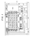
- FIG. 3 is a view for explaining the first substrate before a cell cutting step in the liquid crystal display module of the embodiment according to the present invention
- FIG. 4A and FIG. 4B are views showing the circuit constitution of one example of an electrostatic protective circuit for protecting a pixel part or an electrostatic protective circuit for protecting a peripheral circuit of the embodiment according to the present invention
- FIG. 5A and FIG. 5B are views showing the circuit constitution of another example of the electrostatic protective circuit for protecting the pixel part or the electrostatic protective circuit for protecting the peripheral circuit of the embodiment according to the present invention.
- FIG. 6 is a graph showing a simulation result of voltage-current characteristics when the electrostatic protective circuit adopts the 2-MOS-transistor constitution or the 4-MOS-transistor constitution;
- FIG. 8 is a view for explaining a first substrate before a cell cutting step in a conventional liquid crystal display module.
- FIG. 1 is a perspective view showing the schematic constitution of a liquid crystal display panel of a liquid crystal display module of the embodiment according to the present invention.
- the liquid crystal display module of this embodiment is a miniaturized TFT-type liquid crystal display module used as a display part of a mobile phone.
- the liquid crystal display panel of this embodiment is configured as follows.
- a first substrate also referred to as a TFT substrate or an active matrix substrate (SUB 1 ) on which pixel electrodes, thin film transistors and the like are formed and a second substrate (also referred to as a counter substrate) (SUB 2 ) on which color filters and the like are formed are overlapped to each other with a predetermined gap therebetween.
- Both substrates are adhered to each other using a frame-shaped sealing material formed between both substrates in the vicinity of peripheral portions of both substrates.
- Liquid crystal is filled and sealed in the inside of a space defined by both substrates and the sealing material through a liquid crystal filling port formed in a portion of the sealing material.
- polarizers are laminated to outside portions of both substrates.
- the liquid crystal display module of this embodiment adopts the structure which sandwiches the liquid crystal between the pair of substrates.
- the first substrate (SUB 1 ) has an area larger than an area of the second substrate (SUB 2 ), and a semiconductor chip (Dr) which constitutes a driver for driving the thin film transistors is mounted on a region of the first substrate (SUB 1 ) which does not face the second substrate (SUB 2 ) in an opposed manner. Further, a flexible printed circuit board (FPC) is mounted on a peripheral portion of one side of the region.
- the drive circuit may be incorporated in the first substrate (SUB 1 ) as an integral part thereof by forming the drive circuit using a thin film transistor or the like.
- a material of the substrates is not limited to glass and may be plastic or the like provided that the substrate is made of a material having insulation property.
- counter electrodes are formed on a counter substrate side when the display device adopts a TN-type or VA-type liquid crystal display panel.
- the counter electrodes are formed on a TFT substrate side.
- the present invention when parts of the inner structure of the liquid crystal panel are irrelevant to the present invention, the detailed explanation of these parts is omitted. Further, the present invention is applicable to a liquid crystal panel having any structure.
- FIG. 2 is a block diagram for explaining the first substrate (SUB 1 ) of this embodiment.
- symbol ARSB indicates a pixel part
- symbol TEST indicates an inspection circuit
- symbol FPC indicates a flexible printed circuit board.
- symbol Ar indicated by a dotted frame in FIG. 2 indicates a place where the semiconductor chip (Dr) is mounted.
- Each pixel includes a pixel electrode (PX) and a thin film transistor (TFT) for applying a video voltage to the pixel electrode (PX).
- PX pixel electrode
- TFT thin film transistor
- Gate electrodes of the thin film transistors (TFT) in the row direction are connected to a scanning line (GL), and the scanning line (GL) is connected to a vertical scanning circuit (VSCA).
- Drain electrodes of the thin film transistors (TFT) in the column direction are connected to a video line (DL), and the video line (DL) is connected to a video voltage selection circuit (VDSC).
- VDSC video voltage selection circuit
- the video voltages of red (R), green (G), blue (B) are sequentially inputted to the video voltage selection circuit (VDSC), while the video voltage selection circuit (VDSC) outputs the video voltage of red (R), the video voltage of green (G) and the video voltage of blue (B) which are inputted sequentially to the video line for red (R), the video line for green (G) and the video line for blue (B) respectively.
- a source electrode of the thin film transistor (TFT) is connected to the pixel electrode (PX).
- a liquid crystal capacitance (Clc) is equivalently formed.
- the counter electrode (CT) is connected to a counter voltage line (VCOM).
- a scanning voltage of High level which turns on the thin film transistor (TFT) is sequentially applied to the scanning lines (GL). Due to such an operation, the thin film transistors (TFT) on one display line is sequentially turned on and a video voltage on the video line (DL) is applied to the pixel electrodes (PX) on one display line and hence, an image is displayed on the liquid crystal display panel.
- the liquid crystal display panel of this embodiment is characterized by arranging an electrostatic protective circuit therein. That is, in this embodiment, in regions which are regions other than the pixel region (ARSB) of the first substrate (SUB 1 ) and face the second substrate (SUB 2 ) in an opposed manner, an electrostatic protective circuit (DIODE 1 ) for protecting the pixel part and an electrostatic protective circuit (DIODE 2 ) for protecting the peripheral circuits are formed.
- an electrostatic protective circuit DIODE 1
- DIODE 2 electrostatic protective circuit
- FIG. 3 is a view for explaining the first substrate (SUB 1 ) before a cell cutting step.
- the illustration of the mounting position of the semiconductor chip (Dr) shown in FIG. 2 is omitted.
- the electrostatic protective circuit (DIODE 1 ) for protecting the pixel part is connected.
- the video voltage selection circuit between the at least one video voltage inputting line (LINV) and the line (LINX) other than the video voltage inputting line (LINV) for inputting control signals and the like to the video voltage selection circuit (VDSC), between the plurality of lines (LINX), and between the at least one line (LINX) and a reference voltage line (LVSS) to which a reference voltage (VSS) is applied, the electrostatic protective circuit (DIODE 2 ) for protecting the peripheral circuit is connected.
- the reference voltage VSS is a gate-off voltage which is applied to the gate electrode of the thin film transistor (TFT).
- the electrostatic protective circuit (DIODE 1 ) for protecting the pixel part is connected between the plurality of video lines and, further, the electrostatic protective circuit for protecting the peripheral circuit is connected between the at least one video line and the reference voltage line (LVSS) to which the reference voltage is applied.
- the electrostatic protective circuit (DIODE 1 ) for protecting the pixel part is connected. Still further, between the plurality of lines (LVSC) which is connected to the vertical scanning circuit (VSCA) as well as between the line (LVSC) which is connected to the at least one vertical scanning circuit (VSCA) and the reference voltage line (LVSS) to which the reference voltage (VSS) is applied, the electrostatic protective circuit (DIODE 2 ) for protecting the peripheral circuit is connected.
- the electrostatic protective circuit (DIODE 1 ) for protecting the pixel part is connected.
- the electrostatic protective circuit (DIODE 2 ) for protecting the peripheral circuit is connected between a plurality of lines (LTES) which is connected to the inspection circuit (TEST). Further, also between the at least one line (LTES) which is connected to the inspection circuit (TEST) and the reference voltage line (LVSS) to which the reference voltage (VSS) is applied, the electrostatic protective circuit (DIODE 2 ) for protecting the peripheral circuit is connected.
- one ends (one ends on a side opposite to a side to which grayscale voltages are applied) of the video lines (DL) are connected to the inspection circuit (TEST).
- VDSC video voltage selection circuit
- VSCA vertical scanning circuit
- TEST inspection circuit
- FIG. 4A and FIG. 4B are views showing the circuit constitution of one example of the electrostatic protective circuit (DIODE 1 ) for protecting the pixel part or the electrostatic protective circuit (DIODE 2 ) for protecting the peripheral circuit of this embodiment.
- the electrostatic protective circuit (DIODE 1 ) for protecting the pixel part or the electrostatic protective circuit (DIODE 2 ) for protecting the peripheral circuit of this embodiment is constituted of a pair of diodes (D 1 , D 1 ) which has cathodes thereof connected to each other.
- FIG. 4B shows the circuit constitution of the diode circuit shown in FIG. 4A having the 2-MOS-transistor constitution which is constituted of diode-connected n-type MOS transistors (MT 1 , MT 2 ).
- FIG. 5A and FIG. 5B are views showing the circuit constitution of another example of the electrostatic protective circuit (DIODE 1 ) for protecting the pixel part or the electrostatic protective circuit (DIODE 2 ) for protecting the peripheral circuit of this embodiment.
- either the electrostatic protective circuit (DIODE 1 ) for protecting the pixel part or the electrostatic protective circuit (DIODE 2 ) for protecting the peripheral circuit of this embodiment is constituted of first to fourth diodes (D 11 to D 14 ) which are connected in series, wherein the first diode (D 11 ) and the second diode (D 12 ) have cathodes thereof connected to each other, and the third diode (D 13 ) and the fourth diode (D 14 ) have cathodes thereof connected to each other.
- FIG. 5B shows the circuit constitution of the diode circuit shown in FIG. 5A having the 4-MOS-transistor constitution which is constituted of diode-connected n-type MOS transistors (MT 11 to MT 14 ).
- the electrostatic protective circuit (DIODE 1 , DIODE 2 ) is constituted of diode-connected MOS transistors (MT 1 , MT 2 , MT 11 to MT 14 ), to allow a certain degree of current to flow in the n-type MOS transistor, the MOS transistors (MT 1 , MT 2 , MT 11 to MT 14 ) are required to have a certain degree of gate width (W).
- FIG. 6 and FIG. 7 show a simulation result of voltage-current characteristics when the electrostatic protective circuit adopts the 2-MOS-transistor constitution and the 4-MOS-transistor constitution.
- an applied voltage (unit: V) is taken on an axis of abscissas
- a current (unit: A) is taken on an axis of ordinates.
- a curve ( 1 ) shown in FIG. 6 indicates the voltage-current characteristic when the electrostatic protective circuit adopts the 2-MOS-transistor constitution and the gate width (W) is 6 ⁇ m
- a curve ( 2 ) shown in FIG. 6 indicates the voltage-current characteristic when the electrostatic protective circuit adopts the 4-MOS-transistor constitution and the gate width (W) is 24 ⁇ m.
- a curve ( 1 ) shown in FIG. 7 indicates the voltage-current characteristic when the electrostatic protective circuit adopts the 2-MOS-transistor constitution and the gate width (W) is 10 ⁇ m
- a curve ( 2 ) shown in FIG. 7 indicates the voltage-current characteristic when the electrostatic protective circuit adopts the 4-MOS-transistor constitution and the gate width (W) is 40 ⁇ m.
- the arrangement position of the MOS transistor which constitutes the electrostatic protective circuit falls within a region where light from a backlight is radiated. Accordingly, to take the influence of a leaked current attributed to a photoconductor into consideration, it is desirable to set the gate width (W) of the MOS transistor when the electrostatic protective circuit adopts the 2-MOS-transistor constitution to a value equal to or less than 10 ⁇ m.
- the gate width (W) of the MOS transistor when the electrostatic protective circuit adopts the 2-MOS-transistor constitution is 10 ⁇ m or less.
- the gate width (W) of the MOS transistor when the electrostatic protective circuit adopts the 4-MOS-transistor constitution it is desirable to set the gate width (W) of the MOS transistor when the electrostatic protective circuit adopts the 4-MOS-transistor constitution to a value three times to five times as large as the gate width (W) of the MOS transistor when the electrostatic protective circuit adopts the 2-MOS-transistor constitution.
- the present invention by arranging the electrostatic protective circuits in the inside of the liquid crystal display panel, even in and after the cell cutting step, the breakdown voltage against the static electricity can be enhanced thus preventing electrostatic breakdown attributed to static electricity.
- the electrostatic protective circuits can adopt the 2-MOS-transistor constitution or the 4-MOS-transistor constitution and hence, the electrostatic protective circuits can be arranged with the least arrangement space.
- the electrostatic protective circuit can be manufactured in an n-MOS single channel process, it is possible to set a current which flows in the electrostatic protective circuits during usual driving extremely low.
- the electrostatic protective circuit may be arranged only in the pixel part (ARSB) shown in FIG. 3 or the electrostatic protective circuit may be arranged only in a built-in circuit such as the inspection circuit (TEST), the video voltage selection circuit (VDSC), or the vertical scanning circuit (VSCA) shown in FIG. 3 .
- the inspection circuit TEST
- VDSC video voltage selection circuit
- VSCA vertical scanning circuit
- the present invention is not limited to the liquid crystal display device and is applicable to display devices in general including pixels such as an organic EL display device, for example.
Abstract
Description
Claims (21)
Applications Claiming Priority (2)
| Application Number | Priority Date | Filing Date | Title |
|---|---|---|---|
| JP2006-301088 | 2006-11-07 | ||
| JP2006301088A JP2008116770A (en) | 2006-11-07 | 2006-11-07 | Display device |
Publications (2)
| Publication Number | Publication Date |
|---|---|
| US20080129674A1 US20080129674A1 (en) | 2008-06-05 |
| US8081148B2 true US8081148B2 (en) | 2011-12-20 |
Family
ID=39475146
Family Applications (1)
| Application Number | Title | Priority Date | Filing Date |
|---|---|---|---|
| US11/936,116 Expired - Fee Related US8081148B2 (en) | 2006-11-07 | 2007-11-07 | Display device |
Country Status (2)
| Country | Link |
|---|---|
| US (1) | US8081148B2 (en) |
| JP (1) | JP2008116770A (en) |
Cited By (2)
| Publication number | Priority date | Publication date | Assignee | Title |
|---|---|---|---|---|
| US20140204073A1 (en) * | 2010-08-06 | 2014-07-24 | Semiconductor Energy Laboratory Co., Ltd. | Liquid crystal display device and driving method of the same |
| US20160202578A1 (en) * | 2006-12-27 | 2016-07-14 | Japan Display Inc. | Liquid crystal display device having improved electrostatic discharge resistance |
Families Citing this family (4)
| Publication number | Priority date | Publication date | Assignee | Title |
|---|---|---|---|---|
| KR101033463B1 (en) * | 2008-06-13 | 2011-05-09 | 엘지디스플레이 주식회사 | Array Substrate of Liquid Crystal Display Device |
| TWI379180B (en) * | 2008-12-26 | 2012-12-11 | Delta Electronics Inc | Method of calculating recovery commands for numerical controlled system |
| CN105045007B (en) * | 2015-08-18 | 2019-05-24 | 深圳市华星光电技术有限公司 | A kind of liquid crystal display panel |
| JP2019101128A (en) * | 2017-11-30 | 2019-06-24 | 株式会社ジャパンディスプレイ | Display, and method for manufacturing display |
Citations (6)
| Publication number | Priority date | Publication date | Assignee | Title |
|---|---|---|---|---|
| US5930607A (en) * | 1995-10-03 | 1999-07-27 | Seiko Epson Corporation | Method to prevent static destruction of an active element comprised in a liquid crystal display device |
| US6340963B1 (en) * | 1998-11-26 | 2002-01-22 | Hitachi, Ltd. | Liquid crystal display device |
| US20030063229A1 (en) * | 2001-09-28 | 2003-04-03 | Takuya Takahashi | Liquid crystal display device |
| US20050052391A1 (en) * | 1991-06-14 | 2005-03-10 | Semiconductor Energy Laboratory Co., Ltd. | Electro-optical device and method of driving the same |
| US6947103B2 (en) * | 2000-11-30 | 2005-09-20 | Nec Lcd Technologies, Ltd. | Method of making a reflection type liquid crystal display device |
| US7453420B2 (en) * | 2003-02-14 | 2008-11-18 | Tpo Hong Kong Holding Limited | Display device with electrostatic discharge protection circuitry |
Family Cites Families (8)
| Publication number | Priority date | Publication date | Assignee | Title |
|---|---|---|---|---|
| JP2687667B2 (en) * | 1990-04-17 | 1997-12-08 | 日本電気株式会社 | Matrix electrode substrate and manufacturing method thereof |
| JP3395598B2 (en) * | 1997-09-25 | 2003-04-14 | セイコーエプソン株式会社 | Active matrix substrate manufacturing method and liquid crystal display panel |
| JP2000031476A (en) * | 1998-07-10 | 2000-01-28 | Nissan Motor Co Ltd | Semiconductor device and manufacture thereof |
| JP2002050640A (en) * | 2000-05-22 | 2002-02-15 | Sony Corp | Protection circuit of field effect transistor, and semiconductor device |
| JP2003202599A (en) * | 2003-02-05 | 2003-07-18 | Sharp Corp | Liquid crystal display device and method of manufacturing the same |
| JP4385691B2 (en) * | 2003-09-12 | 2009-12-16 | カシオ計算機株式会社 | Display panel electrostatic protection structure and liquid crystal display panel |
| JP4547957B2 (en) * | 2004-03-24 | 2010-09-22 | セイコーエプソン株式会社 | Electro-optical device and electronic apparatus |
| JP4207858B2 (en) * | 2004-07-05 | 2009-01-14 | セイコーエプソン株式会社 | Semiconductor device, display device and electronic apparatus |
-
2006
- 2006-11-07 JP JP2006301088A patent/JP2008116770A/en active Pending
-
2007
- 2007-11-07 US US11/936,116 patent/US8081148B2/en not_active Expired - Fee Related
Patent Citations (8)
| Publication number | Priority date | Publication date | Assignee | Title |
|---|---|---|---|---|
| US20050052391A1 (en) * | 1991-06-14 | 2005-03-10 | Semiconductor Energy Laboratory Co., Ltd. | Electro-optical device and method of driving the same |
| US7928946B2 (en) * | 1991-06-14 | 2011-04-19 | Semiconductor Energy Laboratory Co., Ltd. | Electro-optical device and method of driving the same |
| US5930607A (en) * | 1995-10-03 | 1999-07-27 | Seiko Epson Corporation | Method to prevent static destruction of an active element comprised in a liquid crystal display device |
| USRE38292E1 (en) * | 1995-10-03 | 2003-10-28 | Seiko Epson Corporation | Method to prevent static destruction of an active element comprised in a liquid crystal display device |
| US6340963B1 (en) * | 1998-11-26 | 2002-01-22 | Hitachi, Ltd. | Liquid crystal display device |
| US6947103B2 (en) * | 2000-11-30 | 2005-09-20 | Nec Lcd Technologies, Ltd. | Method of making a reflection type liquid crystal display device |
| US20030063229A1 (en) * | 2001-09-28 | 2003-04-03 | Takuya Takahashi | Liquid crystal display device |
| US7453420B2 (en) * | 2003-02-14 | 2008-11-18 | Tpo Hong Kong Holding Limited | Display device with electrostatic discharge protection circuitry |
Cited By (7)
| Publication number | Priority date | Publication date | Assignee | Title |
|---|---|---|---|---|
| US20160202578A1 (en) * | 2006-12-27 | 2016-07-14 | Japan Display Inc. | Liquid crystal display device having improved electrostatic discharge resistance |
| US10001685B2 (en) * | 2006-12-27 | 2018-06-19 | Japan Display Inc. | Liquid crystal display device having improved electrostatic discharge resistance |
| US10935856B2 (en) | 2006-12-27 | 2021-03-02 | Japan Display Inc. | Display device with a translucent conductive film |
| US11256151B2 (en) | 2006-12-27 | 2022-02-22 | Japan Display Inc. | Liquid crystal display device having improved electrostatic discharge resistance |
| US11835828B2 (en) | 2006-12-27 | 2023-12-05 | Japan Display Inc. | Liquid crystal display device having improved electrostatic discharge resistance |
| US20140204073A1 (en) * | 2010-08-06 | 2014-07-24 | Semiconductor Energy Laboratory Co., Ltd. | Liquid crystal display device and driving method of the same |
| US8890859B2 (en) * | 2010-08-06 | 2014-11-18 | Semiconductor Energy Laboratory Co., Ltd. | Liquid crystal display device and driving method of the same |
Also Published As
| Publication number | Publication date |
|---|---|
| US20080129674A1 (en) | 2008-06-05 |
| JP2008116770A (en) | 2008-05-22 |
Similar Documents
| Publication | Publication Date | Title |
|---|---|---|
| US10453869B2 (en) | Display apparatus | |
| US7768291B2 (en) | Display device | |
| US8358259B2 (en) | Liquid crystal display device | |
| US7750662B2 (en) | Electro-optical device and electronic apparatus | |
| US7936323B2 (en) | Liquid crystal display device | |
| US9620533B2 (en) | Liquid crystal display having white pixels | |
| JP5024110B2 (en) | Electro-optical device and electronic apparatus | |
| US11264407B2 (en) | Array substrate | |
| US10209574B2 (en) | Liquid crystal display | |
| US20040263460A1 (en) | Active matrix display device | |
| US10964284B2 (en) | Electronic component board and display panel | |
| US8081148B2 (en) | Display device | |
| US6873378B2 (en) | Liquid crystal display panel | |
| WO2020015175A1 (en) | Pixel driving circuit and liquid crystal display device | |
| US10847102B2 (en) | Display device | |
| US20230400941A1 (en) | Display device | |
| JP2007310131A (en) | Active matrix substrate and active matrix display device | |
| JP2008233140A (en) | Manufacturing method of electrooptical device, and electrooptical device | |
| JP2018092013A (en) | Liquid crystal display device and method for driving liquid crystal display device | |
| KR102403688B1 (en) | Display device | |
| US10964251B2 (en) | Pixel array substrate and driving method thereof | |
| KR200406658Y1 (en) | Electrostatic discharge protection circuit in liquid crystal display | |
| WO2011135758A1 (en) | Liquid crystal display device | |
| JP2023142982A (en) | display device | |
| WO2011039903A1 (en) | Liquid crystal display device |
Legal Events
| Date | Code | Title | Description |
|---|---|---|---|
| AS | Assignment |
Owner name: HITACHI DISPLAYS, LTD., JAPAN Free format text: ASSIGNMENT OF ASSIGNORS INTEREST;ASSIGNORS:ABE, HIROYUKI;SUGIYAMA, SAORI;ASUMA, HIROAKI;REEL/FRAME:020490/0673;SIGNING DATES FROM 20080128 TO 20080130 Owner name: HITACHI DISPLAYS, LTD., JAPAN Free format text: ASSIGNMENT OF ASSIGNORS INTEREST;ASSIGNORS:ABE, HIROYUKI;SUGIYAMA, SAORI;ASUMA, HIROAKI;SIGNING DATES FROM 20080128 TO 20080130;REEL/FRAME:020490/0673 |
|
| AS | Assignment |
Owner name: HITACHI DISPLAYS, LTD, JAPAN Free format text: ASSIGNMENT OF ASSIGNORS INTEREST;ASSIGNORS:ABE, HIROYUKI;SUGIYAMA, SAORI;ASUMA, HIROAKI;REEL/FRAME:020541/0034;SIGNING DATES FROM 20080128 TO 20080130 Owner name: HITACHI DISPLAYS, LTD, JAPAN Free format text: ASSIGNMENT OF ASSIGNORS INTEREST;ASSIGNORS:ABE, HIROYUKI;SUGIYAMA, SAORI;ASUMA, HIROAKI;SIGNING DATES FROM 20080128 TO 20080130;REEL/FRAME:020541/0034 |
|
| ZAAA | Notice of allowance and fees due |
Free format text: ORIGINAL CODE: NOA |
|
| ZAAB | Notice of allowance mailed |
Free format text: ORIGINAL CODE: MN/=. |
|
| AS | Assignment |
Owner name: IPS ALPHA SUPPORT CO., LTD., JAPAN Free format text: COMPANY SPLIT PLAN TRANSFERRING FIFTY (50) PERCENT SHARE IN PATENT APPLICATIONS;ASSIGNOR:HITACHI DISPLAYS, LTD.;REEL/FRAME:027092/0684 Effective date: 20100630 Owner name: PANASONIC LIQUID CRYSTAL DISPLAY CO., LTD., JAPAN Free format text: MERGER;ASSIGNOR:IPS ALPHA SUPPORT CO., LTD.;REEL/FRAME:027093/0937 Effective date: 20101001 |
|
| STCF | Information on status: patent grant |
Free format text: PATENTED CASE |
|
| FEPP | Fee payment procedure |
Free format text: PAYOR NUMBER ASSIGNED (ORIGINAL EVENT CODE: ASPN); ENTITY STATUS OF PATENT OWNER: LARGE ENTITY |
|
| FPAY | Fee payment |
Year of fee payment: 4 |
|
| MAFP | Maintenance fee payment |
Free format text: PAYMENT OF MAINTENANCE FEE, 8TH YEAR, LARGE ENTITY (ORIGINAL EVENT CODE: M1552); ENTITY STATUS OF PATENT OWNER: LARGE ENTITY Year of fee payment: 8 |
|
| FEPP | Fee payment procedure |
Free format text: MAINTENANCE FEE REMINDER MAILED (ORIGINAL EVENT CODE: REM.); ENTITY STATUS OF PATENT OWNER: LARGE ENTITY |
|
| LAPS | Lapse for failure to pay maintenance fees |
Free format text: PATENT EXPIRED FOR FAILURE TO PAY MAINTENANCE FEES (ORIGINAL EVENT CODE: EXP.); ENTITY STATUS OF PATENT OWNER: LARGE ENTITY |
|
| STCH | Information on status: patent discontinuation |
Free format text: PATENT EXPIRED DUE TO NONPAYMENT OF MAINTENANCE FEES UNDER 37 CFR 1.362 |
|
| FP | Lapsed due to failure to pay maintenance fee |
Effective date: 20231220 |