US6831309B2 - Unipolar photodiode having a schottky junction contact - Google Patents
Unipolar photodiode having a schottky junction contact Download PDFInfo
- Publication number
- US6831309B2 US6831309B2 US10/322,986 US32298602A US6831309B2 US 6831309 B2 US6831309 B2 US 6831309B2 US 32298602 A US32298602 A US 32298602A US 6831309 B2 US6831309 B2 US 6831309B2
- Authority
- US
- United States
- Prior art keywords
- layer
- photodiode
- unipolar
- light absorption
- band gap
- Prior art date
- Legal status (The legal status is an assumption and is not a legal conclusion. Google has not performed a legal analysis and makes no representation as to the accuracy of the status listed.)
- Expired - Lifetime
Links
- 230000031700 light absorption Effects 0.000 claims abstract description 146
- 238000000034 method Methods 0.000 claims abstract description 33
- 239000004065 semiconductor Substances 0.000 claims description 119
- 239000000758 substrate Substances 0.000 claims description 30
- 229910052751 metal Inorganic materials 0.000 claims description 26
- 239000002184 metal Substances 0.000 claims description 26
- 239000000969 carrier Substances 0.000 claims description 20
- 230000004888 barrier function Effects 0.000 claims description 15
- 238000005286 illumination Methods 0.000 claims description 9
- 230000005684 electric field Effects 0.000 claims description 8
- 239000004020 conductor Substances 0.000 claims description 2
- 230000003247 decreasing effect Effects 0.000 claims 1
- 239000000463 material Substances 0.000 description 22
- 229910000530 Gallium indium arsenide Inorganic materials 0.000 description 17
- 150000001875 compounds Chemical class 0.000 description 16
- 238000000151 deposition Methods 0.000 description 15
- 238000010586 diagram Methods 0.000 description 15
- GPXJNWSHGFTCBW-UHFFFAOYSA-N Indium phosphide Chemical compound [In]#P GPXJNWSHGFTCBW-UHFFFAOYSA-N 0.000 description 12
- 230000008021 deposition Effects 0.000 description 10
- 238000010521 absorption reaction Methods 0.000 description 9
- 230000003287 optical effect Effects 0.000 description 9
- 230000004044 response Effects 0.000 description 8
- 238000004519 manufacturing process Methods 0.000 description 6
- 239000010949 copper Substances 0.000 description 4
- 239000010931 gold Substances 0.000 description 4
- 239000007769 metal material Substances 0.000 description 4
- 229910052782 aluminium Inorganic materials 0.000 description 3
- XAGFODPZIPBFFR-UHFFFAOYSA-N aluminium Chemical compound [Al] XAGFODPZIPBFFR-UHFFFAOYSA-N 0.000 description 3
- MDPILPRLPQYEEN-UHFFFAOYSA-N aluminium arsenide Chemical compound [As]#[Al] MDPILPRLPQYEEN-UHFFFAOYSA-N 0.000 description 3
- 239000000203 mixture Substances 0.000 description 3
- 238000001451 molecular beam epitaxy Methods 0.000 description 3
- RYGMFSIKBFXOCR-UHFFFAOYSA-N Copper Chemical compound [Cu] RYGMFSIKBFXOCR-UHFFFAOYSA-N 0.000 description 2
- BQCADISMDOOEFD-UHFFFAOYSA-N Silver Chemical compound [Ag] BQCADISMDOOEFD-UHFFFAOYSA-N 0.000 description 2
- 230000009471 action Effects 0.000 description 2
- 229910045601 alloy Inorganic materials 0.000 description 2
- 239000000956 alloy Substances 0.000 description 2
- 238000010276 construction Methods 0.000 description 2
- 229910052802 copper Inorganic materials 0.000 description 2
- 239000002019 doping agent Substances 0.000 description 2
- 239000003574 free electron Substances 0.000 description 2
- PCHJSUWPFVWCPO-UHFFFAOYSA-N gold Chemical compound [Au] PCHJSUWPFVWCPO-UHFFFAOYSA-N 0.000 description 2
- 229910052737 gold Inorganic materials 0.000 description 2
- 230000005525 hole transport Effects 0.000 description 2
- 238000000926 separation method Methods 0.000 description 2
- 229910052709 silver Inorganic materials 0.000 description 2
- 239000004332 silver Substances 0.000 description 2
- GYHNNYVSQQEPJS-UHFFFAOYSA-N Gallium Chemical compound [Ga] GYHNNYVSQQEPJS-UHFFFAOYSA-N 0.000 description 1
- 229910052785 arsenic Inorganic materials 0.000 description 1
- RQNWIZPPADIBDY-UHFFFAOYSA-N arsenic atom Chemical compound [As] RQNWIZPPADIBDY-UHFFFAOYSA-N 0.000 description 1
- -1 but not limited to Inorganic materials 0.000 description 1
- 230000015556 catabolic process Effects 0.000 description 1
- 230000008859 change Effects 0.000 description 1
- 238000006243 chemical reaction Methods 0.000 description 1
- 238000005229 chemical vapour deposition Methods 0.000 description 1
- 238000004891 communication Methods 0.000 description 1
- 239000000470 constituent Substances 0.000 description 1
- 238000009826 distribution Methods 0.000 description 1
- 230000000694 effects Effects 0.000 description 1
- 238000005530 etching Methods 0.000 description 1
- 229910052733 gallium Inorganic materials 0.000 description 1
- BHEPBYXIRTUNPN-UHFFFAOYSA-N hydridophosphorus(.) (triplet) Chemical compound [PH] BHEPBYXIRTUNPN-UHFFFAOYSA-N 0.000 description 1
- 229910052738 indium Inorganic materials 0.000 description 1
- APFVFJFRJDLVQX-UHFFFAOYSA-N indium atom Chemical compound [In] APFVFJFRJDLVQX-UHFFFAOYSA-N 0.000 description 1
- 238000003780 insertion Methods 0.000 description 1
- 230000037431 insertion Effects 0.000 description 1
- 238000005468 ion implantation Methods 0.000 description 1
- 230000006855 networking Effects 0.000 description 1
- 229910021420 polycrystalline silicon Inorganic materials 0.000 description 1
- 229920005591 polysilicon Polymers 0.000 description 1
- 238000007493 shaping process Methods 0.000 description 1
- 230000007723 transport mechanism Effects 0.000 description 1
Images


Classifications
-
- H—ELECTRICITY
- H10—SEMICONDUCTOR DEVICES; ELECTRIC SOLID-STATE DEVICES NOT OTHERWISE PROVIDED FOR
- H10F—INORGANIC SEMICONDUCTOR DEVICES SENSITIVE TO INFRARED RADIATION, LIGHT, ELECTROMAGNETIC RADIATION OF SHORTER WAVELENGTH OR CORPUSCULAR RADIATION
- H10F30/00—Individual radiation-sensitive semiconductor devices in which radiation controls the flow of current through the devices, e.g. photodetectors
- H10F30/20—Individual radiation-sensitive semiconductor devices in which radiation controls the flow of current through the devices, e.g. photodetectors the devices having potential barriers, e.g. phototransistors
- H10F30/21—Individual radiation-sensitive semiconductor devices in which radiation controls the flow of current through the devices, e.g. photodetectors the devices having potential barriers, e.g. phototransistors the devices being sensitive to infrared, visible or ultraviolet radiation
-
- Y—GENERAL TAGGING OF NEW TECHNOLOGICAL DEVELOPMENTS; GENERAL TAGGING OF CROSS-SECTIONAL TECHNOLOGIES SPANNING OVER SEVERAL SECTIONS OF THE IPC; TECHNICAL SUBJECTS COVERED BY FORMER USPC CROSS-REFERENCE ART COLLECTIONS [XRACs] AND DIGESTS
- Y02—TECHNOLOGIES OR APPLICATIONS FOR MITIGATION OR ADAPTATION AGAINST CLIMATE CHANGE
- Y02E—REDUCTION OF GREENHOUSE GAS [GHG] EMISSIONS, RELATED TO ENERGY GENERATION, TRANSMISSION OR DISTRIBUTION
- Y02E10/00—Energy generation through renewable energy sources
- Y02E10/50—Photovoltaic [PV] energy
- Y02E10/548—Amorphous silicon PV cells
Definitions
- the invention relates to photodiodes used in optical network receivers.
- the invention relates to photodiodes having a unipolar or uni-traveling-carrier structure.
- Semiconductor photodetectors most notably various forms of photodiodes, absorb incident light in the form of photons and convert the absorbed photons into an electric current.
- the current within a lattice of the semiconductor is often represented in terms of ‘free carriers’ or simply ‘carriers’.
- a photon with sufficient energy interacts with an atom of the semiconductor lattice, an electron associated with the atom moves across an energy band gap from a valence shell or band to a conduction shell or band of the semiconductor. Movement of the electron across the band gap creates a negative carrier, i.e., the electron, and leaves behind a positive carrier known as a ‘hole’.
- a carrier transport mechanism within the semiconductor-based photodetector separates the generated holes and electrons, thereby creating an electric current known generally as a photocurrent.
- both the electron and the hole may act as carriers within the semiconductor and contribute to the photoelectric current.
- the photocurrent thus created enables the photodetector to interact in various ways with an external circuit or system.
- photodiodes find wide-scale application in optical receivers used for optical communication networks.
- Photodetector performance is often summarized in terms of bandwidth, efficiency, maximum current output, and optical wavelength range.
- Bandwidth is a measure of a speed of response of the photodetector to changes in an incident optical signal or light source.
- Efficiency measures how much of the incident optical signal is converted into carriers.
- Maximum current output is typically determined by a saturation condition within the semiconductor of the photodetector while optical wavelength range is a function of certain material properties of the photodetector among other things.
- photodetector performance is limited by a combination of material properties of constituent materials of the photodetector and a structural characteristic of the photodetector associated primarily with a type and/or structure of a given photodetector.
- FIG. 1A illustrates a cross section of a conventional positive-intrinsic-negative (PIN) photodiode 10 .
- the PIN photodiode 10 comprises an intrinsic or lightly doped semiconductor layer 14 (i-layer) sandwiched between a p-type semiconductor layer 12 (p-layer) and an n-type semiconductor layer 15 (n-layer).
- the i-layer 14 is often referred to as a photo-active or a light absorption layer 14 since ideally, photon absorption is primarily confined to the i-layer 14 of the PIN diode 10 .
- a deposited metal such as aluminum (Al), or another conductive material, such as heavily doped polysilicon, form a pair of ohmic contacts 17 a , 17 b , that provide an electrical connection between the PIN photodiode and an external circuit.
- the ohmic contact 17 a connected to the p-layer is called an anode contact 17 a while the ohmic contact 17 b connected to the n-layer is referred to as a cathode contact 17 b .
- the PIN photodiode 10 is formed on and structurally supported by a semi-insulating substrate 19 .
- FIG. 1B illustrates a band diagram 20 of the PIN photodiode 10 illustrated in FIG. 1 A.
- the band diagram 20 depicts energy levels as electron-volts (eV) in a vertical or y-direction and physical length or distance along a conduction path within a device in a horizontal or x-direction.
- eV electron-volts
- the band diagram 20 illustrates a valence band energy level 21 and a conduction band energy level 22 separated by a band gap 23 for each of the layers of the PIN photodiode 10 .
- the hole 30 moves in the i-layer 14 to the p-layer 12 under the influence of an electric potential gradient formed by an inherently lower energy level of the p-layer 12 for holes.
- the hole combines with an electron supplied by the external circuit (not illustrated).
- the electron 32 moves in the i-layer 14 toward the n-layer 15 under the influence of an electric potential gradient formed by the inherently lower energy level of the n-layer 15 for electrons.
- Electrons in the n-layer 15 enter the cathode contact (not illustrated).
- the drift or movement of electrons 32 and holes 30 in the i-layer 14 drives an electric current in the n-layer 15 , the p-layer 12 , and the external circuit.
- a photodiode that overcomes the bandwidth limitation associated with hole transport time. Moreover, it would be advantageous if such a photodiode were similar in complexity to the PIN photodiode and provided good efficiency. Such a photodiode would solve a longstanding need in the area of photodiodes for optical networking.
- the present invention provides a unipolar or uni-traveling-carrier (UTC) photodiode that employs a Schottky contact (SC) as a cathode contact.
- UTC unipolar or uni-traveling-carrier
- SC Schottky contact
- the present invention provides a metal Schottky contact directly on a collector layer or intrinsic layer (i-layer) of the photodiode.
- the Schottky cathode contact on the i-layer is substituted for an n-type semiconductor layer in contact with an i-layer of a conventional UTC PIN photodiode.
- a unipolar photodiode comprises a first semiconductor or light absorption layer in a first conduction type having a first doping concentration.
- the light absorption layer has a band gap energy that facilitates light absorption.
- the unipolar photodiode further comprises a second semiconductor or collector layer having a second doping concentration and a collector band gap energy.
- the light absorption layer is adjacent to and in contact with a first side of the collector layer.
- the collector band gap energy is greater than the light absorption band gap energy, such that the collector layer is relatively non-conducive to light absorption.
- the unipolar photodiode further comprises a Schottky cathode contact adjacent to and in contact with a second side of the collector layer. The second side is opposite the first side.
- the unipolar photodiode further comprises an anode contact indirectly interfaced to the light absorption layer.
- a method of detecting incident light using the unipolar photodiode and a method of constructing the unipolar photodiode of the present invention are provided.
- the present invention provides a simpler UTC or unipolar photodiode construction than that of the conventional UTC photodiode, yet provides a saturation current equivalent to that of the conventional UTC photodiode. Moreover, while simpler than the conventional UTC photodiode, the SC-UTC photodiode of the present invention exhibits improved bandwidth and efficiency relative to the conventional UTC photodiode. Furthermore in some embodiments, an order of the layers within the Schottky contact unipolar photodiode of the present invention is advantageously reversed compared to that of the conventional UTC PIN photodiode facilitated, in part, by the use of the Schottky cathode contact according to the present invention. Certain embodiments of the present invention have other advantages in addition to and in lieu of the advantages described hereinabove.
- FIG. 1A illustrates a cross sectional view of a conventional vertically illuminated positive-intrinsic-negative (PIN) photodiode.
- PIN positive-intrinsic-negative
- FIG. 1B illustrates a band diagram for the PIN photodiode illustrated in FIG. 1 A.
- FIG. 2A illustrates a cross sectional view of a vertically illuminated Schottky contact unipolar photodiode according to an embodiment of the present invention.
- FIG. 2B illustrates a band diagram for the Schottky contact unipolar photodiode embodiment illustrated in FIG. 2 A.
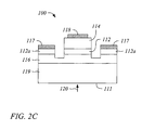
- FIG. 2C illustrates a cross sectional view of a vertically illuminated Schottky contact unipolar photodiode having an indirectly interfaced ohmic contact 117 according to an embodiment of the present invention.
- FIG. 3A illustrates a cross sectional view of the vertically illuminated Schottky contact unipolar photodiode according to another embodiment of the present invention.
- FIG. 3B illustrates a band diagram for the Schottky contact unipolar photodiode embodiment illustrated in FIG. 3 A.
- FIG. 4A illustrates a band diagram of a Schottky contact unipolar photodiode having both a graded band gap layer and a carrier block layer according to an embodiment of the present invention.
- FIG. 4B illustrates a band diagram of another embodiment of a Schottky contact unipolar photodiode having a graded doping concentration layer according to the present invention.
- FIG. 5A illustrates a perspective view of an embodiment of the Schottky contact unipolar photodiode according to the present invention.
- FIG. 5B illustrates a perspective view of another embodiment of the Schottky contact unipolar photodiode according to the present invention.
- FIG. 6A illustrates a cross sectional view of a conventional vertically illuminated uni-traveling-carrier (UTC) photodiode.
- UTC uni-traveling-carrier
- FIG. 6B illustrates a band diagram for the UTC photodiode illustrated in FIG. 6 A.
- FIG. 7 illustrates a flow chart of a method of detecting incident light using a Schottky contact unipolar photodiode according to an embodiment of the present invention.
- FIG. 8 illustrates a flow chart of a method of constructing a Schottky contact unipolar photodiode according to an embodiment of the present invention.
- FIG. 2A illustrates a cross sectional view of a vertically illuminated Schottky contact unipolar photodiode 100 according to an embodiment, of the present invention.
- FIG. 2B illustrates a band diagram for the Schottky contact unipolar photodiode 100 embodiment illustrated in FIG. 2 A.
- vertical illumination is not intended to limit the scope of the present invention in any way.
- one skilled in the art may readily manufacture the Schottky contact unipolar photodiode 100 in the form of a horizontally illuminated or waveguide photodiode without undue experimentation given the discussion hereinbelow.
- the Schottky contact unipolar photodiode 100 comprises a light absorption layer 112 , a carrier-traveling or collector layer 114 affixed to a side of the light absorption layer 112 , a carrier block layer 116 affixed to a side of the light absorption layer 112 opposite the side to which the collector layer 114 is affixed, and a Schottky metal contact 118 connected directly to and covering a portion of a surface of the collector layer 114 opposite a side of the collector layer 114 that is connected to the light absorption layer 112 .
- the Schottky contact unipolar photodiode 100 further comprises an ohmic contact 117 connected to the carrier block layer 116 .
- the Schottky metal contact 118 serves as a cathode contact while the ohmic contact 117 functions as an anode contact for the Schottky contact unipolar photodiode 100 according to the present invention.
- the Schottky contact unipolar photodiode 100 may be mounted or formed on a supporting surface of a semi-insulating substrate 119 .
- the light absorption layer 112 is a semiconductor of a first conduction type, for example, a p-type semiconductor.
- the semiconductor of the light absorption layer 112 preferably has a band gap that facilitates light absorption/conversion in an optical wavelength range of interest.
- the light absorption layer 112 semiconductor has a doping concentration sufficient to maintain charge neutrality in at least part of the layer 112 under a biased state or condition.
- the semiconductor of the light absorption layer 112 is chosen such that the band gap energy is less than or approximately equal to a mean or an average energy (e.g., hv) of an incident photon.
- the doping concentration of the layer 112 is such that the carriers are essentially undepleted within at least a portion of the light absorption layer 112 .
- the photodiode 100 may be operated with a bias of zero volts (V), such as when an output current level is low, preferably the light absorption layer 112 remains essentially undepleted within at least a portion of the light absorption layer 112 when a reverse bias of up to a breakdown voltage of the photodiode 100 is applied to the photodiode 100 .
- the light absorption layer 112 may be a III-V compound semiconductor such as, but not limited to, gallium-aluminum-arsenide (GaAlAs) doped with a p-type dopant.
- III-V semiconductors for use as the light absorption layer 112 include, but are not limited to, indium-phosphide (InP) or materials lattice-matched to InP, gallium-arsenide-antimonide (GaAsSb), Gallium-indium-arsenide (GaInAs), aluminum-gallium-arsenide-antimonide (AlGaAsSb), aluminum-gallium-indium-arsenide (AlGaInAs), gallium-indium-arsenide-phosphide (GaInAsP).
- InP indium-phosphide
- GaAsSb gallium-arsenide-antimonide
- GaInAs Gallium-indium-arsen
- Such p-type III-V compound semiconductors and related materials are known to have band gaps that are suitable for use as the light absorption layer 112 .
- doping concentrations sufficient to allow such semiconductors to remain essentially undepleted under bias conditions may be readily achieved in practice.
- One skilled in the art can readily determine and produce a suitable doping concentration without undue experimentation.
- the collector layer 114 of the photodiode 100 is a semiconductor having a dopant concentration that is lower than that of the light absorption layer 112 . Moreover, the semiconductor of the collection layer 114 preferably has a band gap that is greater than that of the light absorption layer 112 . In some embodiments, the collector layer 114 is a lightly doped or undoped semiconductor and is essentially similar to an intrinsic layer (i-layer) of a conventional PIN photodiode 10 in that it supports the drift or transport field, and thus is identified with an intrinsic layer (i-layer) 14 .
- the collector layer 114 preferably has a band gap that is greater than that of the light absorption layer 112 . Additionally, a small offset of the conduction band energy of the light absorption layer 21 a relative to the conduction band energy of the collector layer 21 b often is desirable to facilitate movement of electrons from the light absorption layer 112 into the collector layer 114 . As a result, there is a mismatch 24 ′ in the valence band energy levels 22 between the light absorption layer 112 and the collector layer 114 . The mismatch 24 ′ manifests itself as an abrupt change from a relatively higher valence energy level 22 a within the light absorption layer 112 to a lower valence energy level 22 b just inside the collector layer 114 .
- mismatch 24 ′ prevents or impedes holes generated and/or present in the light absorption layer 112 from entering the collector layer 114 .
- mismatch 24 ′ acts a barrier 24 to the movement of holes into the collector layer 114 .
- the mismatch 24 ′ acts as the barrier 24
- the barrier 24 is neither essential nor necessary according to the present invention since the field in the collector layer 114 naturally opposes the movement of holes into the collector layer 114 .
- the holes preferentially drift and/or diffuse (i.e., move) away from the collector layer 114 and toward the carrier block layer 116 and the ohmic contact 117 .
- Holes also move away from the collector layer 114 and toward the carrier block layer 116 and the ohmic contact 117 in small fields generated by the photocurrent such that current continuity is maintained throughout the photodiode 100 .
- the collector layer 114 may be a III-V compound semiconductor. However, as already noted, the collector layer 114 has a lower doping concentration and higher bandgap energy than that of the light absorption layer 112 . Thus, the collector layer 114 may be a lightly doped or undoped, semiconductor such as, but not limited to, indium phosphide (InP).
- InP indium phosphide
- collector layer 114 include, but are not limited to, undoped or lightly doped materials that are lattice matched to InP, undoped or lightly doped gallium-arsenide-antimonide (GaAsSb), undoped or lightly doped gallium-indium-arsenide (GaInAs), undoped or lightly doped aluminum-gallium-arsenide-antimonide (AlGaAsSb), undoped or lightly doped aluminum-gallium-indium-arsenide (AlGaInAs), undoped or lightly doped gallium-indium-arsenide-phosphide (GaInAsP).
- GaAsSb undoped or lightly doped gallium-arsenide-antimonide
- GaInAs undoped or lightly doped gallium-indium-arsenide
- AlGaAsSb undoped aluminum-gallium-indium-arsenide-phosphide
- the collector layer 114 preferably has a larger band gap than that of the light absorption layer 112 , if GaInAs is employed as the light absorption layer 112 semiconductor in an exemplary photodiode 100 of the present invention, then InP may be used for the collector layer 114 semiconductor.
- a conduction band matching layer may be employed between the light absorption layer 112 and the collector layer 114 to reduce the heterojunction conduction band energy barrier that may form between the light absorption layer 112 and the collector layer 114 . If a conduction band energy of the collector layer 114 is greater than that of the light absorption layer 112 , then there will be a barrier to transport of electrons from the light absorption layer 112 into the collector layer 114 .
- the conduction band matching layer may reduce the photodiode response time by effectively reducing this barrier and facilitating the movement of electrons from the light absorption layer 112 into the collector layer 114 .
- the conduction band matching layer may be a III-V compound semiconductor or combination of III-V compound semiconductors.
- the semiconductor(s) of the conduction band matching layer may be of a first conduction type, for example p-type and/or of a second conduction type, for example n-type.
- the conduction band matching layer may be a III-V compound semiconductor such as, but not limited to, a single gallium-indium-arsenide-phosphide (GaInAsP) layer or several layers of differing GaInAsP alloy compositions, each one being appropriately doped.
- GaInAsP gallium-indium-arsenide-phosphide
- doped III-V semiconductors for use as the conduction band matching layer include, but are not limited to, indium-phosphide (InP) or materials lattice-matched to InP, gallium-arsenide-antimonide (GaAsSb), Gallium-indium-arsenide (GaInAs), aluminum-gallium-arsenide-antimonide (AlGaAsSb), aluminum-gallium-indium-arsenide (AlGaInAs).
- InP indium-phosphide
- GaAsSb gallium-arsenide-antimonide
- GaInAs Gallium-indium-arsenide
- AlGaAsSb aluminum-gallium-arsenide-antimonide
- AlGaInAs aluminum-gallium-indium-arsenide
- AlGaInAs aluminum-gallium-indium-arsenide
- the carrier block layer 116 is a semiconductor of the first conduction type, for example a p-type semiconductor.
- the semiconductor of the carrier block layer 116 has a band gap that is greater than the band gap of the light absorption layer 112 .
- the band gap of the carrier block layer 116 being greater than that of the light absorbing layer 112 at least reduces, and preferably greatly reduces or substantially prevents, a chance that free electrons created in the light absorption layer 112 will move in a direction of the carrier block layer 116 .
- the band gap of the carrier block layer 116 acts a barrier 25 to movement of electrons from the light absorption layer 112 into the carrier block layer 116 .
- the electrons preferentially flow away from the boundary.
- the carrier block layer 116 effectively directs electron flow toward the collector layer 114 and ultimately to the cathode contact 118 .
- the relatively greater band gap of the carrier block layer 116 reduces a chance that a photon incident on the carrier block layer 116 will create a pair of free carriers within the layer 116 .
- the photo-generation of the carriers is essentially and preferentially confined to the light absorption layer 112 .
- the photocurrent consists mainly of photo-generated electrons flowing from the light absorption layer 112 through the collector layer 114 and into the Schottky contact 118 .
- the carrier block layer 116 may be a p-type III-V compound semiconductor.
- the carrier block layer 116 has a band gap that is greater than the band gap of the light absorption layer 112 .
- the carrier block layer 116 may be a relatively heavily doped p-type III-V compound semiconductor, such as, but not limited to, gallium-indium-arsenide-phosphide (GaInAsP).
- suitable p-type heavily doped III-V semiconductors for use as the carrier block layer 116 include, but are not limited to, indium-phosphide (InP) or materials lattice-matched to InP, gallium-arsenide-antimonide (GaAsSb), Gallium-indium-arsenide (GaInAs), aluminum-gallium-arsenide-antimonide (AlGaAsSb), aluminum-gallium-indium-arsenide (AlGaInAs), gallium-aluminum-arsenide (GaATAs).
- InP indium-phosphide
- GaAsSb gallium-arsenide-antimonide
- GaInAs Gallium-indium-arsenide
- AlGaAsSb aluminum-gallium-indium-arsenide-antimonide
- AlGaInAs aluminum-gallium-indium-arsenide
- GaATAs gallium-a
- a valence band matching layer may be employed between the light absorption layer 112 and the carrier block layer 116 to reduce the heterojunction valence band energy barrier that may form between the light absorption layer 112 and the carrier block layer 116 .
- An offset in the valence band energy between the light absorption layer 112 and the carrier block layer 116 will result in a barrier to transport of holes from the light absorption layer 112 into the carrier block layer 116 or from the carrier block layer 116 into the absorption layer 112 .
- the valence band matching layer may reduce the series resistance by facilitating the movement of holes from the light absorption layer 112 into the carrier block layer 116 .
- the valence band matching layer may be a III-V compound semiconductor or combination of III-V compound semiconductors.
- the semiconductor(s) of the valence band matching layer may be of a first conduction type, for example p-type.
- the valence band matching layer may be a III-V compound semiconductor such as, but not limited to, a single gallium-indium-arsenide-phosphide (GaInAsP) layer or several layers of differing GaInAsP alloy compositions, each one appropriately doped.
- GaInAsP gallium-indium-arsenide-phosphide
- valence band matching layer examples include, but are not limited to, indium-phosphide (InP) or materials lattice-matched to InP, gallium-arsenide-antimonide (GaAsSb), Gallium-indium-arsenide (GaInAs), aluminum-gallium-arsenide-antimonide (AlGaAsSb), aluminum-gallium-indium-arsenide (AlGaInAs).
- the valence band matching layer is similar in concept to the conduction band matching layer described hereinabove.
- One skilled in the art can readily determine and produce suitable semiconductor layers with appropriate doping concentrations for the valence band matching layer without undue experimentation.
- the Schottky contact 118 is a metal contact material on a surface of and in intimate contact with the collector layer 114 .
- the metal contact material in intimate contact with the collector layer 114 forms a Schottky barrier at an interface or boundary between the metal material of the contact 118 and the lattice of the semiconductor of the collector layer 114 .
- the metal contact material forms the Schottky contact 118 .
- the metal material of the Schottky contact 118 may be any metal used in semiconductor manufacture for producing a metal contact including, but not limited to, aluminum (Al), silver (Ag), gold (Au), or copper (Cu).
- Al aluminum
- Au gold
- Cu copper
- the ohmic contact 117 is an electrical contact that is adjacent to and interfaced with the carrier block layer 116 .
- a metal ohmic contact 117 is formed using any electrically conductive metal including, but not limited to, aluminum (Al), silver (Ag), gold (Au), or copper (Cu).
- Al aluminum
- Au gold
- Cu copper
- the ohmic contact 117 may either directly or indirectly interfaced to the carrier block layer 116 .
- ohmic contact 117 is formed by depositing metal or another suitable contact material on a surface of the carrier block layer 116 .
- FIG. 2A illustrates an embodiment of a directly interfaced ohmic contact 117 .
- another layer may be employed between the ohmic contact 117 and the carrier block layer 116 .
- the other layer may be employed to improve a performance of the ohmic contact 117 such as, but not limited to series resistance and/or contact 117 adhesion.
- a layer of heavily doped semiconductor material may be used to indirectly connect the ohmic contact 117 to the carrier block layer 116 .
- a portion 112 a of a layer used to create the light absorption layer 112 may be physically separated from the light absorption layer 112 during processing to form the photodiode 100 .
- the physically separated portion 112 a may be then employed to indirectly interface the ohmic contact 117 to the carrier block layer 116 .
- FIG. 2C illustrates a cross sectional view of a vertically illuminated Schottky contact unipolar photodiode having an indirectly interfaced ohmic contact 117 according to an embodiment of the present invention.
- the use of another layer may facilitate a lower resistance ohmic contact 117 .
- Indirect interfacing enables insertion of a material that is more conducive to forming an ohmic contact 117 with a lower overall resistance (e.g., materials with a lower band gap energy than that of the carrier block layer 116 ).
- the use of a valence band matching layer as described hereinabove may further reduce the series resistance.
- the valence matching layer further reduces series resistance by facilitating the movement of holes from the carrier block layer 116 into the light absorption layer 112 , thereby further reducing series resistance of the ohmic contact 117 .
- the vertically illuminated Schottky contact unipolar photodiode 100 as illustrated in FIG. 2A may be illuminated from a direction, hereinafter referred to as from ‘below’ the photodiode 100 , which corresponds to a side 111 represented by a location of the semi-insulating substrate 119 .
- reference to ‘below’ means the side 111 of the photodiode 100 that is opposite to a side of the photodiode 100 that comprises the Schottky contact 118 .
- incident light 120 in the form of photons may enter the photodiode 100 from the below side 111 passing through the semi-insulating substrate 119 .
- the semi-insulating substrate 119 is preferably transparent or at least translucent to the incident light 120 .
- the carrier block layer 116 is transparent or translucent to the incident light 120 .
- photons pass through the semi-insulating substrate 119 and the carrier block layer 116 and enter the light absorption layer 112 .
- the photons having an energy E p approximately equal to hv, may impact atoms of the semiconductor lattice and generate a pair of free carriers (e.g., holes and electrons).
- the electrons thus generated are directed preferentially to diffuse toward the collector layer 114 , in part, by the presence and action of the carrier block layer 116 and the barrier 25 formed thereby.
- the electrons Upon entering the collector layer 114 , the electrons are accelerated toward the Schottky contact 118 by an energy gradient and/or electric field in the collector layer 114 .
- the electrons absorbed by the contact 118 .
- the electrons of the photocurrent may flow through an external circuit attached to the Schottky contact 118 .
- the holes generated by absorption of a photon are directed preferentially to diffuse toward the carrier block layer 116 and therethrough to the ohmic contact 117 .
- the principal drift or movement direction is due in large part to the presence of the energy mismatch barrier 24 at the collector layer 114 edge, as already described hereinabove.
- the holes may combine or become filled with electrons supplied by the external circuit. In other words, the holes are essentially ‘absorbed’ by the ohmic contact 117 .
- the photocurrent is almost entirely a function of the electrons flowing from the light absorption layer 112 into the Schottky contact 118 .
- a response time of the photodiode 100 advantageously is reduced compared to that of the conventional PIN photodiode.
- the reduced response time results in an increased bandwidth for the Schottky contact unipolar photodiode 100 of the present invention relative to the conventional PIN photodiode.
- FIG. 3A illustrates a cross sectional view of a vertically illuminated Schottky contact unipolar photodiode 200 according to another embodiment of the present invention.
- the embodiment illustrated in FIG. 3A is a Schottky contact unipolar photodiode 200 comprising a light absorbing layer that has or produces a quasi-field within the layer.
- a ‘quasi-field’ is an electric field created primarily through a controlled use of various materials within the layer wherein the created field essentially and preferentially acts only on minority carriers (e.g., electrons) within a neutrally charged layer (e.g., light absorption layer 212 ) of a semiconductor.
- FIG. 3B illustrates a band diagram for the Schottky contact unipolar photodiode 200 embodiment illustrated in FIG. 3 A.
- vertical illumination is not intended to limit the scope of the present invention in any way.
- one skilled in the art may readily produce the Schottky contact unipolar photodiode 200 that employs a quasi-field in the form of a horizontally illuminated or waveguide photodiode without undue experimentation according to the present invention.
- the Schottky contact unipolar photodiode 200 comprises a light absorbing, ‘graded band gap’ layer 212 , a carrier-traveling or collector layer 214 affixed to a side of the light absorption layer 212 , and a Schottky metal contact 218 connected directly to and covering a portion of a surface of the collector layer 214 .
- the surface of the collector layer 214 to which the Schottky contact 218 is connected is opposite the side of the collector layer 214 that is connected to the light absorption layer 212 .
- the Schottky contact unipolar photodiode 200 further comprises an ohmic contact 217 connected to the graded band gap layer 212 .
- the Schottky metal contact 218 serves as a cathode contact while the ohmic contact 217 functions as an anode contact for the Schottky contact unipolar photodiode 200 according to the present invention.
- the Schottky contact unipolar photodiode 200 may be mounted or formed on a supporting surface of a semi-insulating substrate 219 .
- the collector layer 214 is essentially similar to the collector layer 114 described hereinabove with respect to the Schottky contact unipolar photodiode 100 and is connected to one side of the graded band gap layer 212 .
- the collector layer 214 comprises a semiconductor that is lightly doped or undoped relative to a doping level of the graded band gap layer 212 .
- the ohmic contact 217 , Schottky contact 218 , and semi-insulating substrate 219 are essentially similar to the ohmic contact 117 , the Schottky contact 118 , and semi-insulating substrate 119 , respectively, described hereinabove for the previous disclosed photodiode 100 .
- the Schottky contact 218 is connected directly to a side of the collector layer 214 that is opposite the side connected to the graded band gap layer 212 .
- the Schottky contact unipolar photodiode 200 of the present embodiment differs from the Schottky contact unipolar photodiode 100 embodiment in that the graded band gap layer 212 replaces the light absorption layer 112 .
- the graded band gap layer 212 or a portion thereof, absorbs incident light and converts photons therein into free carriers.
- the graded band gap layer 212 provides a quasi-field that directs a movement of minority carriers (e.g., electrons) toward the collector layer 214 and away from the ohmic contact 217 .
- the carrier block layer 116 of the previously disclosed photodiode 100 embodiment may be omitted in the Schottky contact unipolar photodiode 200 of the present embodiment.
- the graded band gap layer 212 comprises semiconductor material having a graded band gap. Moreover, the grading is ‘towards’ a side of the layer 212 connected to the collector layer 214 . In other words, the band gap of the graded band gap layer 212 semiconductor material generally increases as a function of distance from the side of the layer 212 that is connected to the collector layer 214 . As such, the band gap is generally smaller at the side of the graded band gap layer 212 connected to the collector layer 214 than at an opposite side.
- the graded band gap is depicted graphically as a gradual increase in an energy level difference between the conduction band level 21 and valence band level 22 within the graded band gap layer 212 in the band diagram illustrated in FIG. 3 B.
- the graded band gap layer 212 has a doping concentration (e.g., p-type doping) that exceeds a predetermined level such that at least a portion of the layer 212 is not depleted when the photodiode 200 is reversed biased.
- a doping concentration e.g., p-type doping
- the band gap grading may be created in practice by forming a III-V compound semiconductor layer in which a composition of the compound semiconductor is adjusted appropriately throughout a thickness of the layer 212 .
- a composition of the compound semiconductor is adjusted appropriately throughout a thickness of the layer 212 .
- GaInAsP is employed to construct the graded band gap layer 212
- ratios of the component elements, gallium, indium, arsenic, and phosphorous may be controlled and changed as a function of distance to effect a desired grading of the band gap while maintaining a desired lattice constant.
- a 100 meV or greater difference in band gap from one side of the graded band gap layer 212 to the other or opposite side may be produced by gradually varying the Ga/In/As/P ratio within the layer 212 .
- One skilled in the art is familiar with forming semiconductor layers having graded band gaps.
- a result of grading the band gap to decrease in a direction toward the collector layer 214 is that the quasi-field is created.
- minority carriers e.g., electrons
- a 100 meV difference in band gap across the graded band gap layer 212 produces a suitably strong quasi-field for directing the electron movement.
- the quasi-field reduces a response time of the photodiode 200 by preferentially accelerating the free electrons created by light absorption within the graded band gap layer 212 in a direction of the collector layer 214 .
- the graded band gap layer 212 of the photodiode 200 embodiment illustrated in FIGS. 3A and 3B may be divided into a first region or portion 212 a and a second region or portion 212 b .
- the first portion 212 a is adjacent to the collector layer 214 .
- the first portion 212 a is a portion of the graded band gap layer 212 wherein the band gap is less than or equal to an approximate energy hv of an incident photon.
- the second portion 212 b is adjacent to the semi-insulating substrate 219 when present.
- the band gap of the second portion 212 b is generally greater than the energy of an incident photon within the second portion 212 b .
- the first portion 212 a essentially preferentially provides absorption of incident light with a concomitant generation of free carriers while the second portion 212 b contributes relatively fewer free carriers through light absorption.
- the first portion 212 a may be considered to be a light absorption portion 212 a functionally equivalent to the light absorption layer 112 of the photodiode 100 .
- the second portion 212 b having a band gap that is generally higher than the band gap of the first portion 212 a may be thought of as being functionally equivalent to the carrier block layer 116 of the photodiode 100 .
- the entire graded band gap layer 212 as a whole actually acts to direct the electrons to move toward the collector layer 214 due to the presence of the quasi-field.
- the entire graded band gap layer 212 essentially replaces the carrier block layer 116 of the photodiode 100 .
- a carrier block layer 216 may be used in addition to the graded band gap layer 212 ′.
- a band diagram of a Schottky contact unipolar photodiode 200 ′ having a graded band gap layer 212 ′ and further comprising a carrier block layer 216 is illustrated in FIG. 4 A.
- the carrier block layer 216 preferably has a band gap that is greater than that of a highest band gap in the graded band gap layer 212 ′. More preferably, the highest band gap of the graded band gap layer 212 ′ is less than or equal to the energy of an incident photon, while the band gap of the carrier block layer 216 is greater than the energy of the incident photon.
- a Schottky contact unipolar photodiode 200 ′′ may be realized wherein the graded band gap layer 212 , 212 ′ is replaced with a layer 212 ′′ having a graded doping concentration (e.g., p-type).
- FIG. 4B illustrates a band diagram of the Schottky contact unipolar photodiode 200 ′′ that employs a graded doping concentration layer 212 ′′.
- the graded doping concentration layer 212 ′′ has a doping concentration that is graded towards the collector layer 214 in much the same way as the band gap of the graded band gap layer 212 , 212 ′ is graded toward the collector layer 214 .
- the graded doping concentration creates an electric field in which both electrons and holes move.
- the graded doping concentration layer 212 ′′ acts to direct the electrons to move toward the collector layer 214 due to the presence of the electric field.
- the graded doping concentration layer 212 ′′ acts to direct the holes to move toward the block layer 216 due to the presence of the electric field.
- the Schottky contact unipolar photodiode 200 ′′ employing the graded doping concentration layer 212 ′′ may be realized with or without (not illustrated) a carrier block layer 216 and still be within the scope of the present invention.
- FIG. 5A illustrates a perspective view of an embodiment of the Schottky contact unipolar photodiode 100 according to the present invention.
- FIG. 5A illustrates an exemplary ‘pillbox’ or concentric-contact style embodiment of the Schottky contact unipolar photodiode 100 according to the present invention.
- ‘top’ means a side of the photodiode 100 comprising the Schottky contact 118 , such as the orientation of the photodiode 100 in illustrated in FIG. 5 A.
- ‘bottom’ as used herein, means a side of the photodiode 100 opposite to the top. As illustrated in FIG.
- the ohmic contact 117 that serves as the anode contact, lies on top of and is connected to the carrier block layer 116 . Furthermore, the ohmic contact 117 is annularly disposed around a central stack portion of the photodiode 100 .
- the central stack portion comprises a portion of the carrier block layer 116 , the light absorption layer 112 on top of the carrier block layer 116 , the collector layer 114 on top of the light absorption layer 112 , and the Schottky contact 118 cathode contact at the top of the stack.
- FIG. 5A illustrates the photodiode 100 embodiment supported by the semi-insulating substrate 119 .
- Incident light preferably enters the exemplary photodiode 100 from below, passing through the semi-insulating substrate 119 , before entering the photodiode 100 .
- a similar configuration to that illustrated for FIG. 5A may be used to construct the other embodiments 200 , 200 ′, 200 ′′ of the photodiode 200 described hereinabove.
- the vertically illuminated photodiode 100 , 200 , 200 ′, 200 ′′ embodiment of FIG. 5A light passes through the carrier block layer 116 , 216 with little absorption. A fraction of the light is absorbed as it passes through light absorption layer 112 , 212 . The light then passes through the collector layer 114 , 214 essentially without absorption and is then reflected by the Schottky metal contact 118 , 218 . The reflected light again passes through the photodiode layers but in a reverse direction. Upon passing through the light absorption layer 112 , 212 , a second time, more of the light is absorbed. As a result of the light reflecting from the Schottky metal contact 118 , 218 , more photocurrent is produced and the photodiode has higher efficiency than if there were no reflection.
- FIG. 5B illustrates a perspective view of another exemplary embodiment of the Schottky contact unipolar photodiode 100 according to the present invention.
- the exemplary embodiment illustrated in FIG. 5B is well suited for realizing a horizontally illuminated or waveguide photodiode as opposed to the primarily vertically illuminated application of the photodiode 100 embodiment illustrated in FIG. 5 A.
- Incident light enters this exemplary embodiment of the photodiode 100 from below when vertically illuminated.
- incident light When employed as a horizontally illuminated or waveguide photodiode, incident light preferably enters the light absorption layer 112 from a side. More preferably, incident light enters from a side that is perpendicular to a long dimension of the photodiode 100 .
- An arrow 120 in FIG. 5B illustrates a path taken by incident light in an embodiment of the horizontally illuminated or waveguide photodiode.
- a similar configuration to that illustrated in FIG. 5B may be employed to construct the other embodiments 200 , 200 ′, 200 ′′ of the photodiode 200 described hereinabove according to the present invention.
- the Schottky unipolar photodiode 100 may be operated in a reverse biased condition or state.
- the reverse bias may be applied to the photodiode 100 such that a reverse bias voltage appears across an interface between the Schottky contact 118 and the collector layer 114 .
- a relationship may be specified between a thickness W of the layer 112 and a conductivity ⁇ of the layer 112 .
- the layer conductivity ⁇ and the layer thickness W satisfy a relationship given in equation (1) J 0 ⁇ W 2 ⁇ ⁇ ⁇ ⁇ ⁇ ⁇ E ⁇ - L q ( 1 )
- the layer conductivity ⁇ and the layer thickness W preferably satisfy a relationship given in equation (2) ⁇ 0 W ⁇ J 0 ⁇ ( W - x ) W ⁇ ⁇ ⁇ ⁇ ( x ) ⁇ ⁇ ⁇ x ⁇ ⁇ ⁇ ⁇ E ⁇ - L q ( 2 )
- Equations (1) and/or (2) may be similarly applied to the Schottky contact unipolar photodiode 200 , 200 ′, 200 ′′ by one skilled in the art without undue experimentation.
- FIG. 6A illustrates a cross sectional view of a conventional unipolar or uni-traveling-carrier (UTC) photodiode 300 .
- FIG. 6B illustrates a band diagram of the conventional UTC photodiode 300 .
- the conventional UTC-photodiode 300 comprises a light absorption layer 312 , a carrier traveling or collector layer 314 connected to a first side of the light absorption layer 312 and a carrier block layer 316 connected to a second side of the light absorption layer 312 , the second side being opposite the first side.
- the carrier traveling or collector layer 314 is adjacent and connected to an electrode layer 315 .
- a cathode contact 317 a is formed by connecting a first ohmic contact 317 a to the electrode layer 315 that underlies the carrier traveling or collector layer 314 .
- An anode contact 317 b is formed by connecting a second ohmic contact 317 b to the carrier block layer 316 at the top of the layer stack.
- the electrode layer 315 is a heavily doped semiconductor having a conduction type that differs from that of the light absorption layer 312 . For example, if the light absorption layer 312 is a p-type semiconductor, the electrode layer 315 is a heavily doped n-type semiconductor.
- the conventional UTC photodiode is formed by stacking in succession the electrode layer 315 on top of a semi-insulating substrate 319 , the carrier traveling or collector layer 314 on top of the electrode layer 315 , the light absorption layer 312 on top of the carrier traveling or collector layer 314 , and then carrier block layer 316 on top of the light absorption layer 312 .
- the first ohmic contact 317 a or cathode contact, is connected to an exposed portion of the electrode layer 315 while the second ohmic contact 317 b , or anode contact, is connected to the carrier block layer 316 at a top of the stack.
- the Schottky contact unipolar photodiode 100 , 200 , 200 ′, 200 ′′ of the present invention differs markedly from a conventional unipolar or uni-traveling-carrier (UTC) photodiode in several ways.
- the Schottky contact unipolar photodiode 100 , 200 , 200 ′, 200 ′′ comprises a Schottky contact 118 , 218 instead of the first ohmic contact 317 a as the cathode contact.
- the Schottky contact 118 , 218 advantageously simplifies the photodiode 100 , 200 , 200 ′, 200 ′′ by eliminating a need for the electrode layer 315 of the conventional UTC photodiode.
- the Schottky contact 118 , 218 offers specific performance advantages that allow a faster response time and higher efficiency than are possible with an ohmic contact. Additionally, the Schottky contact 118 , 218 can provide a lower effective series resistance than is possible with an ohmic contact in this application. A lower series resistance reduces the response time of the photodiode 100 , 200 , 200 ′, 200 ′′. Moreover, in the vertically illuminated embodiment of the photodiode 100 represented by FIG. 5A, the light reflection from the Schottky metal contact can be greater than that from an ohmic contact, resulting in a higher efficiency than possible from a photodiode employing an ohmic contact.
- FIG. 7 illustrates a method 400 of detecting incident light using a Schottky contact unipolar photodiode according to the present invention.
- the method 400 comprises absorbing 410 light in the form of photons in a photo-active portion of the photodiode.
- the method 400 further comprises generating 420 an electron and a hole from an absorbed photon.
- the method 400 further comprises preferentially moving 430 the generated electron into a collector portion of the photodiode while simultaneously preferentially moving 440 the hole away from the collector portion.
- preferentially moving 430 the generated electron comprises employing a carrier block layer having a band gap greater than that of the light absorption portion on a side of the light absorption portion opposite that of the collector portion.
- the band gap difference between the light absorption portion and the carrier block layer effectively impedes the flow of electrons towards the carrier block layer thereby causing electrons to preferentially move towards the collector portion.
- a graded band gap or a graded doping concentration may be employed to generate a quasi-field that preferentially moves 430 the electrons toward the collector portion of the photodiode.
- the electric field in the collector portion and the band gap difference between the collector portion and the light absorption portion effectively prevent holes from moving into the collector portion thereby preferentially moving 440 the holes away from the collector portion. Furthermore, the electromotive force to maintain the continuity of photocurrent throughout the photodiode and external circuit preferentially moves 440 the holes away from the collector portion and toward the ohmic contact.
- the method 400 further comprises receiving 450 the generated electrons from the collector portion with a Schottky metal contact.
- the electrons received by the Schottky metal contact are those that are generated in the light absorption portion and travel through the collector portion.
- the Schottky metal contact acts as a cathode of the photodiode.
- the method 400 may further comprise absorbing 460 holes at an ohmic contact acting as an anode contact.
- FIG. 8 illustrates a flow chart of a method 500 of constructing a Schottky contact unipolar photodiode according to the present invention.
- the method 500 comprises forming 510 a carrier block layer on or in a top surface of a semi-insulating substrate.
- the carrier block layer may be formed 510 using an epitaxial deposition of a semiconductor layer on the top surface of the semi-insulating substrate. Any and all methods of epitaxial deposition suitable for semiconductor layer deposition may be employed to form 510 the carrier block layer.
- a p-type III-V compound semiconductor may be formed 510 using molecular-beam epitaxy (MBE) or metal-organic chemical vapor deposition (MOCVD) for epitaxial deposition.
- MBE molecular-beam epitaxy
- MOCVD metal-organic chemical vapor deposition
- the carrier block layer may be formed 510 within the top surface of the semi-insulating substrate by selective doping of the substrate such as by ion implantation. Selective doping forms 510 the carrier block layer as a ‘well’ within the lattice of the semi-insulating substrate.
- the formed 510 carrier block layer has the characteristics of the carrier block layer 116 described hereinabove with respect to the Schottky contact unipolar photodiode 100 .
- the method further comprises depositing 520 a light absorption layer on top of the formed 510 carrier block layer.
- the deposition 520 may be by way of epitaxial deposition or any other deposition methodology known in the art and suitable for semiconductor manufacturing.
- a p-type III-V compound semiconductor may be deposited 520 on top of carrier block layer using MBE or MOCVD.
- the deposited 520 light absorption layer is similar to and has characteristics of the light absorption layer 112 described hereinabove with respect to the Schottky contact unipolar photodiode 100 .
- the method further comprises depositing 530 a collector layer on top of the light absorption layer.
- the deposition 530 may be by way of epitaxial deposition or any other deposition methodology suitable for manufacturing semiconductors.
- an n-type or undoped III-V compound semiconductor may be deposited 530 on top of the light absorption layer using MBE or MOCVD.
- the deposited 530 light absorption layer is similar to and has characteristics of the collector layer 114 described hereinabove with respect to the Schottky contact unipolar photodiode 100 .
- the method further comprises creating 540 a Schottky contact on a top surface of the collector layer.
- the Schottky contact may be created on the top surface of the collector layer by any methodology suitable for creating a Schottky contact.
- a metal may be evaporated or sputter deposited onto the top surface of the collector layer after any oxide layer that may have formed thereon is removed.
- the created 540 Schottky contact has characteristics of the Schottky contact 118 described hereinabove with respect to the Schottky contact unipolar photodiode 100 .
- the created 540 Schottky contact is a cathode contact for the photodiode.
- the method optionally further comprises creating 550 an ohmic contact on a top surface in a carrier block layer or in a light absorption layer.
- the ohmic contact may be created 550 on a top surface in the carrier block layer or a top surface of another layer on top of a top surface of the carrier block layer such as a separated portion of the light absorption layer.
- the ohmic contact may be created 550 by any methodology suitable for creating an ohmic contact.
- a metal may be evaporated or sputter deposited onto a top surface in the carrier block layer or a top surface of another layer on a top surface of the carrier block layer.
- the metal is deposited after any oxide layer that may have formed thereon is removed from the surface.
- the created 550 ohmic contact preferably has characteristics of the ohmic contact 117 described hereinabove with respect to the Schottky contact unipolar photodiode 100 .
- the created 550 ohmic contact is an anode contact for the photodiode.
- An ohmic anode contact may be formed and connected to the carrier block layer or light absorption layer simultaneously with creating 540 the Schottky contact.
- the ohmic contact may be formed and connected at another time during the method 500 of constructing.
- etching or another form of mechanical shaping of one or more of the layers of the photodiode may be performed at various times during the method 500 of constructing and still be within the scope of the present invention.
- the Schottky contact unipolar photodiode 100 may readily adapt an embodiment 500 ′ of the method 500 to construct the Schottky contact unipolar photodiode 200 , 200 ′, 200 ′′ in which the light absorption layer is replaced by a graded band gap layer or a graded doping layer.
- depositing 520 the light absorption layer may be replaced by depositing 520 ′ a graded band gap or a graded doping layer.
- forming 510 the carrier block layer may be omitted since the carrier block layer is optional for the Schottky contact unipolar photodiode 200 , 200 ′, 200 ′′ having a graded band gap layer and/or a graded doping concentration layer.
Landscapes
- Light Receiving Elements (AREA)
Priority Applications (2)
| Application Number | Priority Date | Filing Date | Title |
|---|---|---|---|
| US10/322,986 US6831309B2 (en) | 2002-12-18 | 2002-12-18 | Unipolar photodiode having a schottky junction contact |
| JP2003421345A JP2004200703A (ja) | 2002-12-18 | 2003-12-18 | ショットキー接合接点を備えたユニポールフォトダイオード |
Applications Claiming Priority (1)
| Application Number | Priority Date | Filing Date | Title |
|---|---|---|---|
| US10/322,986 US6831309B2 (en) | 2002-12-18 | 2002-12-18 | Unipolar photodiode having a schottky junction contact |
Publications (2)
| Publication Number | Publication Date |
|---|---|
| US20040119129A1 US20040119129A1 (en) | 2004-06-24 |
| US6831309B2 true US6831309B2 (en) | 2004-12-14 |
Family
ID=32593081
Family Applications (1)
| Application Number | Title | Priority Date | Filing Date |
|---|---|---|---|
| US10/322,986 Expired - Lifetime US6831309B2 (en) | 2002-12-18 | 2002-12-18 | Unipolar photodiode having a schottky junction contact |
Country Status (2)
| Country | Link |
|---|---|
| US (1) | US6831309B2 (enExample) |
| JP (1) | JP2004200703A (enExample) |
Cited By (9)
| Publication number | Priority date | Publication date | Assignee | Title |
|---|---|---|---|---|
| US20060039666A1 (en) * | 2001-12-27 | 2006-02-23 | Knights Andrew P | In-line light sensor |
| US20060071224A1 (en) * | 2002-09-23 | 2006-04-06 | Osram Opto Semiconductor Gmbh | Radiation-emitting semiconductor component |
| US20060131579A1 (en) * | 2004-12-17 | 2006-06-22 | Commissariat A L'energie Atomique | Semiconductor photodetector, device for multispectrum detection of electromagnetic radiation using such a photodetector and method for using such a device |
| US20090184383A1 (en) * | 2006-03-31 | 2009-07-23 | Ucl Business Plc | Photodetector |
| US20110018033A1 (en) * | 2008-03-26 | 2011-01-27 | Sumitomo Chemical Company, Limited | Semiconductor wafer, semiconductor device, and method of manufacturing a semiconductor device |
| US20110089516A1 (en) * | 2008-08-06 | 2011-04-21 | Canon Kabushiki Kaisha | Rectifier |
| US8334550B1 (en) | 2011-06-09 | 2012-12-18 | Northrop Grumman Systems Corporation | Unipolar diode with low turn-on voltage |
| CN111312827A (zh) * | 2018-11-27 | 2020-06-19 | 上海新微技术研发中心有限公司 | 一种单向载流子传输光电探测器及其制造方法 |
| US20230253516A1 (en) * | 2020-07-22 | 2023-08-10 | Nippon Telegraph And Telephone Corporation | Photodetector |
Families Citing this family (14)
| Publication number | Priority date | Publication date | Assignee | Title |
|---|---|---|---|---|
| GB2417126A (en) * | 2004-08-09 | 2006-02-15 | Qinetiq Ltd | Method for fabricating lateral semiconductor device |
| US7339209B2 (en) * | 2005-09-07 | 2008-03-04 | The Boeing Company | Integrated semiconductor structure including a heterojunction bipolar transistor and a Schottky diode |
| US8044435B2 (en) * | 2006-11-14 | 2011-10-25 | Lockheed Martin Corporation | Sub-pixel nBn detector |
| US8138583B2 (en) * | 2007-02-16 | 2012-03-20 | Cree, Inc. | Diode having reduced on-resistance and associated method of manufacture |
| KR100872717B1 (ko) * | 2007-06-22 | 2008-12-05 | 엘지이노텍 주식회사 | 발광 소자 및 그 제조방법 |
| US8084739B2 (en) * | 2008-07-16 | 2011-12-27 | Infrared Newco., Inc. | Imaging apparatus and methods |
| US8928036B2 (en) * | 2008-09-25 | 2015-01-06 | California Institute Of Technology | High operating temperature barrier infrared detector with tailorable cutoff wavelength |
| KR101308761B1 (ko) * | 2009-09-07 | 2013-09-17 | 스미토모덴키고교가부시키가이샤 | Ⅲ-ⅴ족 화합물 반도체 수광 소자, ⅲ-ⅴ족 화합물 반도체 수광 소자를 제작하는 방법, 수광 소자 및 에피택셜 웨이퍼 |
| JP5630213B2 (ja) * | 2010-10-28 | 2014-11-26 | 富士通株式会社 | 光検出素子 |
| JP6162401B2 (ja) * | 2012-12-28 | 2017-07-12 | 株式会社東芝 | 光半導体デバイス |
| US10014424B2 (en) * | 2014-03-13 | 2018-07-03 | Raytheon Company | Reduced junction area barrier-based photodetector |
| US11231382B2 (en) * | 2016-06-15 | 2022-01-25 | William N. Carr | Integrated thermal sensor comprising a photonic crystal |
| US11300453B2 (en) | 2017-06-18 | 2022-04-12 | William N. Carr | Photonic- and phononic-structured pixel for electromagnetic radiation and detection |
| CN111599879B (zh) * | 2020-06-11 | 2022-05-31 | 武汉华星光电技术有限公司 | Pin感光器件及其制作方法、及显示面板 |
Citations (3)
| Publication number | Priority date | Publication date | Assignee | Title |
|---|---|---|---|---|
| US5652435A (en) * | 1995-09-01 | 1997-07-29 | The United States Of America As Represented By The Secretary Of The Air Force | Vertical structure schottky diode optical detector |
| US5818096A (en) * | 1996-04-05 | 1998-10-06 | Nippon Telegraph And Telephone Corp. | Pin photodiode with improved frequency response and saturation output |
| US6104074A (en) * | 1997-12-11 | 2000-08-15 | Apa Optics, Inc. | Schottky barrier detectors for visible-blind ultraviolet detection |
-
2002
- 2002-12-18 US US10/322,986 patent/US6831309B2/en not_active Expired - Lifetime
-
2003
- 2003-12-18 JP JP2003421345A patent/JP2004200703A/ja active Pending
Patent Citations (3)
| Publication number | Priority date | Publication date | Assignee | Title |
|---|---|---|---|---|
| US5652435A (en) * | 1995-09-01 | 1997-07-29 | The United States Of America As Represented By The Secretary Of The Air Force | Vertical structure schottky diode optical detector |
| US5818096A (en) * | 1996-04-05 | 1998-10-06 | Nippon Telegraph And Telephone Corp. | Pin photodiode with improved frequency response and saturation output |
| US6104074A (en) * | 1997-12-11 | 2000-08-15 | Apa Optics, Inc. | Schottky barrier detectors for visible-blind ultraviolet detection |
Non-Patent Citations (5)
| Title |
|---|
| John E. Bowers and Charles A. Burrus, Jr., "Ultrawide-Band Long-Wavelength p-i-n Photodetectors," Journal of Lightwave Technology, vol. LT-5, No. 10, Oct. 1987, pp. 1339-1350. |
| Kazutoshi Kato, "Ultra-Band/High-Frequency Photodetectors," IEEE Trans. on Microwave Theory and Techniques, vol. 47, No. 7, Jul. 1999, pp. 1265-1281. |
| Kirk S. Giboney, "Travelling-Wave Photodetectors," Doctoral Dissertation, University of California, Santa Barbara, Aug. 1995, Chapter 6, Sections 6.1 and 6.2, pp. 123-127. |
| N. Emeis, H. Schumacher, and H. Beneking, "High-Speed GalnAs Schottky Photodetector," Electronic Letters, vol. 21, No. 5, Feb. 1985, pp. 180-181. |
| Tadao Ishibashi et al., "InP/InGaAs Uni-Traveling-Carrier Photodiodes," IEICE Trans. Electron., vol. E83-C, No. 6, Jun. 2000, pp. 938-949. |
Cited By (20)
| Publication number | Priority date | Publication date | Assignee | Title |
|---|---|---|---|---|
| US20110013864A1 (en) * | 2001-12-27 | 2011-01-20 | Andrew Peter Knights | In-line light sensor |
| US8326094B2 (en) * | 2001-12-27 | 2012-12-04 | Kotura, Inc. | In-line light sensor |
| US7826700B2 (en) * | 2001-12-27 | 2010-11-02 | Kotura, Inc. | In-line light sensor |
| US20060039666A1 (en) * | 2001-12-27 | 2006-02-23 | Knights Andrew P | In-line light sensor |
| US7386207B2 (en) * | 2001-12-27 | 2008-06-10 | Kotura, Inc. | In-line light sensor |
| US20090127645A1 (en) * | 2001-12-27 | 2009-05-21 | Andrew Peter Knights | In-line light sensor |
| US7115907B2 (en) * | 2002-09-23 | 2006-10-03 | Osram Opto Semiconductors Gmbh | Radiation-emitting semiconductor component |
| US20060071224A1 (en) * | 2002-09-23 | 2006-04-06 | Osram Opto Semiconductor Gmbh | Radiation-emitting semiconductor component |
| US7619240B2 (en) * | 2004-12-17 | 2009-11-17 | Commissariat A L'energie Atomique | Semiconductor photodetector, device for multispectrum detection of electromagnetic radiation using such a photodetector and method for using such a device |
| US20060131579A1 (en) * | 2004-12-17 | 2006-06-22 | Commissariat A L'energie Atomique | Semiconductor photodetector, device for multispectrum detection of electromagnetic radiation using such a photodetector and method for using such a device |
| US7851782B2 (en) | 2006-03-31 | 2010-12-14 | Ucl Business Plc | Photodetector including multiple waveguides |
| US20090184383A1 (en) * | 2006-03-31 | 2009-07-23 | Ucl Business Plc | Photodetector |
| US20110018033A1 (en) * | 2008-03-26 | 2011-01-27 | Sumitomo Chemical Company, Limited | Semiconductor wafer, semiconductor device, and method of manufacturing a semiconductor device |
| US8431459B2 (en) * | 2008-03-26 | 2013-04-30 | The University Of Tokyo | Semiconductor wafer, semiconductor device, and method of manufacturing a semiconductor device |
| US9087935B2 (en) * | 2008-08-06 | 2015-07-21 | Canon Kabushiki Kaisha | Detector having a Schottky barrier portion and a barrier portion having a rectifying property |
| US20110089516A1 (en) * | 2008-08-06 | 2011-04-21 | Canon Kabushiki Kaisha | Rectifier |
| US8334550B1 (en) | 2011-06-09 | 2012-12-18 | Northrop Grumman Systems Corporation | Unipolar diode with low turn-on voltage |
| CN111312827B (zh) * | 2018-11-27 | 2022-03-01 | 上海新微技术研发中心有限公司 | 一种单向载流子传输光电探测器及其制造方法 |
| CN111312827A (zh) * | 2018-11-27 | 2020-06-19 | 上海新微技术研发中心有限公司 | 一种单向载流子传输光电探测器及其制造方法 |
| US20230253516A1 (en) * | 2020-07-22 | 2023-08-10 | Nippon Telegraph And Telephone Corporation | Photodetector |
Also Published As
| Publication number | Publication date |
|---|---|
| JP2004200703A (ja) | 2004-07-15 |
| US20040119129A1 (en) | 2004-06-24 |
Similar Documents
| Publication | Publication Date | Title |
|---|---|---|
| US6831309B2 (en) | Unipolar photodiode having a schottky junction contact | |
| US6740908B1 (en) | Extended drift heterostructure photodiode having enhanced electron response | |
| US7829915B2 (en) | Avalanche photodiode | |
| US8692301B2 (en) | Nanostructured photodiode | |
| TWI620339B (zh) | 高速光偵測器 | |
| US7795064B2 (en) | Front-illuminated avalanche photodiode | |
| JP2004200703A5 (enExample) | ||
| US8299497B1 (en) | Near-infrared photodetector with reduced dark current | |
| US5679963A (en) | Semiconductor tunnel junction with enhancement layer | |
| US7202102B2 (en) | Doped absorption for enhanced responsivity for high speed photodiodes | |
| US8697554B2 (en) | Lateral collection architecture for SLS detectors | |
| EP3229279A1 (en) | Avalanche photodiode | |
| JP2934294B2 (ja) | アバランシェフォトダイオード | |
| JPH022691A (ja) | 半導体受光素子 | |
| JP2708409B2 (ja) | 半導体受光素子およびその製造方法 | |
| US4390889A (en) | Photodiode having an InGaAs layer with an adjacent InGaAsP p-n junction | |
| CN116705892B (zh) | 一种雪崩二极管 | |
| JPH0656900B2 (ja) | 半導体光素子 | |
| JPH0955522A (ja) | トンネルダイオード | |
| EP0150564A2 (en) | Electronic device comprising a heterojunction | |
| US20250393338A1 (en) | Light receiving device | |
| US12074241B2 (en) | Direct semiconductor solar devices | |
| JPH01194352A (ja) | 受光素子及び集積化受信器 | |
| JPH0575160A (ja) | アバランシエホトダイオードおよびその動作方法 | |
| DEEN | Photodetectors for Optical |
Legal Events
| Date | Code | Title | Description |
|---|---|---|---|
| AS | Assignment |
Owner name: AGILENT TECHNOLOGIES, INC., COLORADO Free format text: ASSIGNMENT OF ASSIGNORS INTEREST;ASSIGNOR:GIBONEY, KIRK S.;REEL/FRAME:013587/0567 Effective date: 20021216 |
|
| STCF | Information on status: patent grant |
Free format text: PATENTED CASE |
|
| FPAY | Fee payment |
Year of fee payment: 4 |
|
| FPAY | Fee payment |
Year of fee payment: 8 |
|
| AS | Assignment |
Owner name: KEYSIGHT TECHNOLOGIES, INC., CALIFORNIA Free format text: ASSIGNMENT OF ASSIGNORS INTEREST;ASSIGNOR:AGILENT TECHNOLOGIES, INC.;REEL/FRAME:033746/0714 Effective date: 20140801 |
|
| FPAY | Fee payment |
Year of fee payment: 12 |