US6806583B2 - Light source - Google Patents
Light source Download PDFInfo
- Publication number
- US6806583B2 US6806583B2 US09/888,857 US88885701A US6806583B2 US 6806583 B2 US6806583 B2 US 6806583B2 US 88885701 A US88885701 A US 88885701A US 6806583 B2 US6806583 B2 US 6806583B2
- Authority
- US
- United States
- Prior art keywords
- light emitting
- emitting diode
- substrate
- recess
- led
- Prior art date
- Legal status (The legal status is an assumption and is not a legal conclusion. Google has not performed a legal analysis and makes no representation as to the accuracy of the status listed.)
- Expired - Lifetime, expires
Links
Images


Classifications
-
- H—ELECTRICITY
- H10—SEMICONDUCTOR DEVICES; ELECTRIC SOLID-STATE DEVICES NOT OTHERWISE PROVIDED FOR
- H10H—INORGANIC LIGHT-EMITTING SEMICONDUCTOR DEVICES HAVING POTENTIAL BARRIERS
- H10H20/00—Individual inorganic light-emitting semiconductor devices having potential barriers, e.g. light-emitting diodes [LED]
- H10H20/80—Constructional details
- H10H20/85—Packages
- H10H20/8506—Containers
-
- H—ELECTRICITY
- H10—SEMICONDUCTOR DEVICES; ELECTRIC SOLID-STATE DEVICES NOT OTHERWISE PROVIDED FOR
- H10W—GENERIC PACKAGES, INTERCONNECTIONS, CONNECTORS OR OTHER CONSTRUCTIONAL DETAILS OF DEVICES COVERED BY CLASS H10
- H10W72/00—Interconnections or connectors in packages
- H10W72/071—Connecting or disconnecting
- H10W72/073—Connecting or disconnecting of die-attach connectors
-
- H—ELECTRICITY
- H10—SEMICONDUCTOR DEVICES; ELECTRIC SOLID-STATE DEVICES NOT OTHERWISE PROVIDED FOR
- H10W—GENERIC PACKAGES, INTERCONNECTIONS, CONNECTORS OR OTHER CONSTRUCTIONAL DETAILS OF DEVICES COVERED BY CLASS H10
- H10W72/00—Interconnections or connectors in packages
- H10W72/071—Connecting or disconnecting
- H10W72/075—Connecting or disconnecting of bond wires
-
- H—ELECTRICITY
- H10—SEMICONDUCTOR DEVICES; ELECTRIC SOLID-STATE DEVICES NOT OTHERWISE PROVIDED FOR
- H10W—GENERIC PACKAGES, INTERCONNECTIONS, CONNECTORS OR OTHER CONSTRUCTIONAL DETAILS OF DEVICES COVERED BY CLASS H10
- H10W72/00—Interconnections or connectors in packages
- H10W72/50—Bond wires
- H10W72/531—Shapes of wire connectors
- H10W72/536—Shapes of wire connectors the connected ends being ball-shaped
-
- H—ELECTRICITY
- H10—SEMICONDUCTOR DEVICES; ELECTRIC SOLID-STATE DEVICES NOT OTHERWISE PROVIDED FOR
- H10W—GENERIC PACKAGES, INTERCONNECTIONS, CONNECTORS OR OTHER CONSTRUCTIONAL DETAILS OF DEVICES COVERED BY CLASS H10
- H10W72/00—Interconnections or connectors in packages
- H10W72/50—Bond wires
- H10W72/531—Shapes of wire connectors
- H10W72/5363—Shapes of wire connectors the connected ends being wedge-shaped
-
- H—ELECTRICITY
- H10—SEMICONDUCTOR DEVICES; ELECTRIC SOLID-STATE DEVICES NOT OTHERWISE PROVIDED FOR
- H10W—GENERIC PACKAGES, INTERCONNECTIONS, CONNECTORS OR OTHER CONSTRUCTIONAL DETAILS OF DEVICES COVERED BY CLASS H10
- H10W72/00—Interconnections or connectors in packages
- H10W72/50—Bond wires
- H10W72/551—Materials of bond wires
- H10W72/552—Materials of bond wires comprising metals or metalloids, e.g. silver
- H10W72/5522—Materials of bond wires comprising metals or metalloids, e.g. silver comprising gold [Au]
-
- H—ELECTRICITY
- H10—SEMICONDUCTOR DEVICES; ELECTRIC SOLID-STATE DEVICES NOT OTHERWISE PROVIDED FOR
- H10W—GENERIC PACKAGES, INTERCONNECTIONS, CONNECTORS OR OTHER CONSTRUCTIONAL DETAILS OF DEVICES COVERED BY CLASS H10
- H10W72/00—Interconnections or connectors in packages
- H10W72/851—Dispositions of multiple connectors or interconnections
- H10W72/874—On different surfaces
- H10W72/884—Die-attach connectors and bond wires
-
- H—ELECTRICITY
- H10—SEMICONDUCTOR DEVICES; ELECTRIC SOLID-STATE DEVICES NOT OTHERWISE PROVIDED FOR
- H10W—GENERIC PACKAGES, INTERCONNECTIONS, CONNECTORS OR OTHER CONSTRUCTIONAL DETAILS OF DEVICES COVERED BY CLASS H10
- H10W90/00—Package configurations
- H10W90/701—Package configurations characterised by the relative positions of pads or connectors relative to package parts
- H10W90/751—Package configurations characterised by the relative positions of pads or connectors relative to package parts of bond wires
- H10W90/754—Package configurations characterised by the relative positions of pads or connectors relative to package parts of bond wires between a chip and a stacked insulating package substrate, interposer or RDL
Definitions
- This invention relates to a light source.
- the invention relates to a light source in the form of a light emitting diode (LED) package suitable for use in an LED matrix video display.
- LED light emitting diode
- LEDs Light emitting diodes
- silicon wafer are commonly used to generate light in a variety of applications ranging from simple low-power indication lights to higher-power LED traffic light clusters and LED matrix video displays.
- the light emitting diode die is assembled into a sealed package containing electrical connections between the die and terminal pads exposed on an outer surface of the package.
- Such a package enables simple connection of the diode to external circuitry and, due the sealing properties of the package, protects the die from external damage.
- FIG. 1 shows one typical surface mount LED package 100 comprising an LED die 110 mounted on a circuit board substrate 120 with a transparent material 130 encapsulating the LED 110 .
- the package includes a pair of conductive interconnects 140 , 142 for coupling the LED to external circuitry.
- a first electrode on the bottom surface of the LED 110 is mounted on and electrically coupled to one of the pair of conductive interconnects 140 .
- a very small wire 144 is then “bonded” or welded at one end to a second electrode on the top surface of the LED 110 , and at the other end to the other one of the pair of conductive interconnects 142 .
- a characteristic of the package of FIG. 1 is that light generated by the LED has a relatively wide directivity. Accordingly, when this type of LED package is incorporated into a video display, the video display will have a relatively wide angle of view in both horizontal and vertical directions. However, a problem with the wide directivity of the LED package is that the light energy emitted by the LED is distributed over a larger angle making the LED appear dimmer in the forward viewing direction. Therefore, video displays incorporating the LED package of FIG. 1 will accordingly appear dimmer to spectators. Video displays are known to require only a viewing angle of around 60 degrees in the horizontal plane and around 30 degrees, in the vertical plane.
- U.S. Pat. No. 5,835,269 assigned to Sony Corporation, Japan proposes using an video display apparatus with a unitary reflecting member in the form of a corrugated sheet.
- the corrugated sheet compensates for the wide directivity of known surface mount LEDs by reflecting stray light back into the forward viewing direction.
- the use of additional structure in the video display adds cost and complexity to the manufacture of video displays which is undesirable.
- a light emitting diode package comprising: a planar substrate having an upper surface and a lower surface, a portion of the upper surface defining a recess, said recess having a side wall tapering outwards towards the upper surface; a light emitting diode mounted in the recess of the substrate; a first electrically-conductive interconnect extending between the upper and lower surfaces, the first interconnect having a terminal on the upper surface coupled to the light emitting diode and an exposed pad on the lower surface for coupling to external circuitry; a second electrically-conductive interconnect extending between the upper and lower surfaces, the second interconnect having a terminal on the upper surface coupled to the light emitting diode and a conductive pad on the lower surface for coupling to external circuitry; and a transparent encapsulant material bonded to the first surface of the substrate to encapsulate the light emitting diode, the encapsulant material being molded to form a focussing ellip
- a light emitting diode package in accordance with the invention has the advantage that light energy emitted by the light emitting diode is concentrated by a combination of reflection from the walls of the substrate recess and by refraction from the focussing ellipsoidal dome.
- the light emitting diode package also provides the additional advantage that by mounting the light emitting diode in the recess of the substrate the package occupies a smaller volume.
- the focussing ellipsoidal dome is shaped to concentrate light within a range of angles in the horizontal and vertical planes.
- the light emitting diode package is thus optimised for use in LED matrix video displays that require only certain viewing angles in the horizontal and vertical planes.
- the side wall of the recess is plated with a metallic layer presenting a silvered reflective surface to the light emitting diode.
- the silvered reflective surface provides improved reflectivity over previously employed gold layers which present a golden appearance to the light emitting diode.
- the metallic layer forms the terminal of the first interconnect.
- the substrate defines first and second vias extending between the upper and lower surfaces, a portion of each of the first and second interconnects extending through the first and second vias respectively.
- Each of the conductive pads of the first and second interconnects may include a gold plated layer for electrically coupling to external circuitry.
- FIG. 1 is a cross-sectional side view of a known surface mount LED package
- FIG. 2 is an orthogonal projection showing front, plan and side views of a surface mount LED package in accordance with the invention
- FIG. 3 is a flowchart illustrating exemplary steps employed during the manufacture of the surface mount LED package shown in FIG. 2;
- FIGS. 4 to 17 are cross-sectional side views of the surface mount LED package of FIG. 2 at different stages in a manufacturing process
- FIG. 18 is a plan view showing the top of the surface mount LED package shown in FIG. 17;
- FIG. 19 is a plan view showing the bottom of the surface mount LED package shown in FIG. 17;
- FIG. 20 is a plan view showing the top of the surface mount LED package of FIG. 5 at an early stage of manufacture
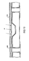
- FIGS. 21 to 23 are plan views of UV masks employed in the manufacturing process steps shown in FIGS. 6 and 10 .
- an LED package 200 which can be surface mounted onto a printed circuit board by, for example, reflow soldering or possibly manual soldering.
- the dimensions of the LED package are preferably 2 millimeters long by 1.25 millimeters wide by 1.2 millimeters tall.
- the surface mount LED package 200 includes a rectangular planar substrate 210 , such as an epoxy or glass laminate, a polyester or polyamide board, a bismaleimidetraizine (BT) resin board, or a thermosetting polyphenylene ether board.
- An upper surface 212 of the substrate includes a conic-section shaped recess 220 positioned centrally on the upper surface.
- the recess 220 comprises a generally circular floor 222 , and a curved side wall 224 tapering concentrically outwards from the floor towards a circular edge 226 on the upper surface 212 .
- the light emitting element of the LED package 200 is provided by a light emitting diode (LED) die 230 which is mounted centrally in the recess 220 of the substrate 210 .
- LED light emitting diode
- two thin gold wires 240 , 242 are electrically coupled at one end to the LED die 230 in order to supply an electric current across a semiconductor junction of the LED die.
- the other ends of the gold wires 240 , 242 are electrically coupled to respective terminals on the upper surface 212 of the substrate 210 .
- the terminals on the upper surface 212 are in turn coupled to a pair of conductive pads 250 , 252 on a lower surface 214 of the substrate 210 by a pair of electrically conductive vias, further details of which will be described later.
- the pair of conductive pads 250 , 252 which are exposed on the lower surface of the substrate provide two generally planar surfaces suitable for surface mounting the bottom of the LED package onto a printed circuit board.
- a transparent or translucent encapsulant material 260 is bonded to the upper surface 212 of the substrate 210 so as to encapsulate the terminals on the upper surface 212 , the gold wires 240 , 242 , and the LED die 230 .
- the encapsulant material is shaped to form a focussing ellipsoidal dome over the light emitting diode.
- the ellipsoidal shape of the encapsulation dome optimises the surface mount LED package for use in video matrix displays. As illustrated in FIG. 2, the major axis radius of curvature of the ellipse shown in the front view is relatively large so as to provide a wide viewing angle of approximately 120 degrees.
- Such a wide viewing angle would be ideally configured in the horizontal plane as is well known in the field of video displays.
- the minor axis radius of curvature of the ellipse shown in the side view is relatively small so as to provide a narrow viewing angle of approximately 60 degrees.
- Such as narrow viewing angle would be ideally configured in the vertical plane as is well known in the field of video displays.
- FIG. 3 is a flowchart illustrating, by way of example, the process steps 300 to 350 employed during the manufacture of the surface mount LED package shown in FIG. 2 .
- the manufacturing process is actually designed to manufacture multiple surface mount LED packages in one batch.
- the starting material for the manufacturing process is a large glass-fibre laminate board which is divided into an array or grid of identical rectangular units.
- a board may, for example, be an FR4 type substrate with a glass transition phase of 180 degrees centigrade.
- the board has an array of units 40 units wide by 20 units long, and has dimensions of approximately 70 millimeters by 70 millimeters by 0.4 millimeters.
- Each rectangular unit on the board forms the basis of the rectangular substrate 210 of the LED package in FIG. 2 .
- the same processing steps 300 , 310 , 320 , 330 , and 340 are applied to each rectangular unit prior to physical separation of the individual units in the sawing step 350 .
- the processing of multiple units on a large board enables the units to be handled more accurately.
- the processing steps will be explained with reference to a single rectangular unit on the board. However, it is understood that the steps will apply to all units on the board.
- the first step 300 in the manufacturing process involves preparing the units of the board for the die attach step 310 .
- the board fabrication step 300 is illustrated sequentially in FIGS. 4 to 14 .
- the bare glass-fiber board unit 400 is first plated on the upper and lower surfaces with copper 410 using standard plating techniques.
- each rectangular unit 400 on the board is drilled with two differently shaped drill bits 430 , 450 as illustrated in FIG. 5 .
- two holes 420 , 425 at opposite corners of the rectangular unit are drilled using a first cylindrically shaped drill bit 430 .
- These via-like holes 420 , 425 extend between the upper and lower surfaces of the board and through the copper plating 410 .
- a conical-section shaped recess 440 is drilled in the upper surface of the board centrally on the rectangular unit by a second cylindrically shaped drill bit 450 having a tapered or chamfered end.
- the drill bits remove the copper plating 410 in the drilling areas, leaving surfaces of the board exposed in the two holes 420 , 425 and in the recess 440 . These exposed areas are then coated with a film of graphite such that the whole surface of the unit becomes electrically conductive.
- the drilled unit is subjected to a series of photochemical etching processes which selectively deposit metallic layers in predetermined regions on the unit surface.
- the first photochemical etching processes is illustrated in FIG. 6 .
- the photochemical etching process comprises applying a dry film 600 made from photosensitive resistive material on the upper and lower surfaces of the unit 400 .
- Photomasks 610 , 612 are then applied above and below the upper and lower dry films 600 respectively.
- the photomasks 610 , 612 shown respectively in plan in FIGS. 21 and 22, are generally transparent except for opaque regions which define where a metallic layer should be deposited.
- the unit 400 With the photomasks in position on the unit 400 , the unit is exposed above and below to ultraviolet (UV) radiation.
- UV radiation ultraviolet
- the regions on the dry film corresponding to the transparent areas on the photomask are selectively hardened by exposure to the UV light. These hardened areas form a chemically-resistant etch mask whilst the unexposed and unhardened regions of the dry film are dissolvable in a suitable etchant, such as chromic acid solution or ferric chloride. Consequently, upon chemically etching away the dry film, an appropriate mask 700 is formed on the upper and lower surfaces of the unit 400 as illustrated in FIG. 7 .
- a suitable etchant such as chromic acid solution or ferric chloride
- FIG. 8 illustrates the result of electrolytically plating the unit with copper 800 and nickel 810 . Because the mask is electrically insulating, no plating occurs over the mask region. In contrast, the remainder of the unit is electrically conductive (including the holes and the recess) and so plating occurs everywhere except the mask region.
- the plated areas define a pair of interconnections on the upper and lower surface of the unit 400 for the LED die.
- the hardened mask region can be removed with a suitable hot organic stripper to leave the unit in the form illustrated in FIG. 9 .
- a second photochemical etching process is then applied to the unit 400 on the upper surface only.
- a dry film 605 made of photosensitive resistive material is applied to the upper surface of the unit 400 .
- a photomask 614 shown in plan in FIG. 23, is then applied over the dry film and the upper surface of the unit 400 is exposed to UV light.
- the photomask exposes only the recess area to UV light such that the dry film hardens over the recess, and remains in place while the obscured regions are dissolved away by means of a suitable etchant.
- FIG. 11 shows the result of this photomasking.
- FIG. 11 shows a coating of flash gold 820 after the hardened mask region has been removed using a suitable hot organic stripper.
- the unwanted copper layers exposed on the outside of the unit 400 are easily removed leaving just the nickel coated recess and the gold coated interconnects as shown in FIG. 14 .
- the last stage in the board fabrication step 300 is to seal the holes 420 , 425 with a thermosetting polymer such as a solder resist.
- a thermosetting polymer such as a solder resist.
- the next step 310 in the manufacturing process is to mount or attach an LED die 230 in the recess 440 .
- the first stage of this die attach step involves dispensing or dotting a small amount of electrically conductive silver epoxy 720 on the floor or base of the recess.
- the next stage involves picking and placing an LED die 230 onto the silver epoxy in the recess as shown in FIG. 15 .
- the final stage of the die attach step involves curing the silver epoxy together with the rest of the unit 400 in a box oven at approximately 180 degree centigrade for a period of approximately one hour. The cured silver epoxy fixes the die in place in the recess and provides good heat conductivity away from the die.
- a wire bonding step 320 is employed in the present embodiment to electrically couple the two sides of the semiconductor junction of the LED die to two electrically isolated terminals on the upper side of the unit board.
- the two terminals are provided by the gold plated layers 822 , 824 at opposite ends of the unit board.
- the wire bonding process creates a ball joint between one end of gold wire and a bond pad on the LED die, and a wedge joint between the other end of the wire and the gold plated terminal on the unit board.
- a suitable apparatus and method for forming such a wire bond is described in U.S. Pat. No. 4,600,138.
- the resulting wire bonded LED die is illustrated in FIG. 16 .
- the batch processing of multiple units is completed in the transfer mold step 330 in which an epoxy encapsulant is molded using a known transfer molding process over the upper surface of the unit 400 .
- the mold is of comparable length and width to the original glass fibre board and comprises an array of ellipsoidal mold cups to compliment the array of units on the board.
- the mold process includes a first step of clamping the mold onto the upper surface of the board such that the array of mold cups are positioned to compliment the array of units on the board.
- the second step is to “transfer” a molding compound into the mold cups under elevated temperature and pressure conditions.
- the molding compound could be an MG18 epoxy, available from Dexter Hysol, USA, which is heated to approximately 155 degrees centigrade and is transferred into the mold under a pressure of 1500 kilo Pascals.
- the array of units undergo a post mold curing step 340 in which the units are baked in a box oven for a period of approximately 3 hours at a temperature of approximately 150 degrees centigrade. This curing step hardens the encapsulation epoxy so that it can withstand exposure to external impact and abrasion.
- the cured encapsulant serves to focus light emitted from the LED die but also provides a barrier layer that prevents moisture and other materials from contacting and damaging the LED die 30 .
- the cured encapsulated unit is shown in detail in FIG. 17 .
- Individual LED packages are produced in the final sawing step in which of individual units on the board array are sawn apart.
- a 0.2 millimeter dicing saw available from Disco Abrasive Systems Inc., Mountain View, Calif., is used to separate the units.
- Detail views of the final surface mount LED package are shown in FIGS. 17, 18 and 19 .
- the invention may be practiced otherwise than as specifically described.
- the nickel plating on the recess which presents a silvered surface to the LED die could be replaced with silver plating to form a silvered surface.
Landscapes
- Led Device Packages (AREA)
- Transforming Electric Information Into Light Information (AREA)
Abstract
Description
Claims (2)
Applications Claiming Priority (2)
| Application Number | Priority Date | Filing Date | Title |
|---|---|---|---|
| MYPI20002918 | 2000-06-28 | ||
| MYPI20002918 | 2000-06-28 |
Publications (2)
| Publication Number | Publication Date |
|---|---|
| US20020047130A1 US20020047130A1 (en) | 2002-04-25 |
| US6806583B2 true US6806583B2 (en) | 2004-10-19 |
Family
ID=19749463
Family Applications (1)
| Application Number | Title | Priority Date | Filing Date |
|---|---|---|---|
| US09/888,857 Expired - Lifetime US6806583B2 (en) | 2000-06-28 | 2001-06-25 | Light source |
Country Status (4)
| Country | Link |
|---|---|
| US (1) | US6806583B2 (en) |
| EP (1) | EP1168461B1 (en) |
| JP (1) | JP4926337B2 (en) |
| DE (1) | DE60130520T2 (en) |
Cited By (26)
| Publication number | Priority date | Publication date | Assignee | Title |
|---|---|---|---|---|
| US20030232461A1 (en) * | 2002-06-04 | 2003-12-18 | Bolken Todd O. | Methods for packaging image sensitive electronic devices |
| US20040099875A1 (en) * | 2002-11-26 | 2004-05-27 | Lin Jung Kan | Structure of surface mount device light emitting diode |
| US20040189170A1 (en) * | 2001-02-15 | 2004-09-30 | Integral Technologies, Inc. | Low cost lighting circuits manufactured from conductive loaded resin-based materials |
| US20040223339A1 (en) * | 2003-05-06 | 2004-11-11 | Ji-Mei Tsuei | Light source device |
| US20040257191A1 (en) * | 2001-08-31 | 2004-12-23 | Rudiger Muller | Fuse component comprising an optical indicator |
| US20060043407A1 (en) * | 2004-08-26 | 2006-03-02 | Kabushiki Kaisha Toshiba | Semiconductor light emitting apparatus |
| US20060043461A1 (en) * | 2002-11-20 | 2006-03-02 | Stmicroelectronics S.R.L. | Process for manufacturing a byte selection transistor for a matrix of non volatile memory cells and corresponding structure |
| US20060186429A1 (en) * | 2005-02-22 | 2006-08-24 | Chew Tong F | Semiconductor light emitting device and method of manufacture |
| US7105863B1 (en) | 2005-06-03 | 2006-09-12 | Avago Technologies Ecbu Ip (Singapore) Pte. Ltd. | Light source with improved life |
| US20070201247A1 (en) * | 2006-02-28 | 2007-08-30 | Minebea Co., Ltd. | Spread illuminating apparatus |
| US20080278954A1 (en) * | 2005-04-05 | 2008-11-13 | Tir Systems Ltd. | Mounting Assembly for Optoelectronic Devices |
| US20090115313A1 (en) * | 2007-11-07 | 2009-05-07 | Industrial Technology Research Institute | Light emitting device and fabricating method thereof |
| US20100200888A1 (en) * | 2009-02-12 | 2010-08-12 | Hymite A/S | Silicon-Based Sub-Mount for an Opto-Electronic Device |
| US20110012497A1 (en) * | 2009-07-15 | 2011-01-20 | Kyowa Electric Wire Co., Ltd. | Plating structure and method for manufacturing electric material |
| US20110079803A1 (en) * | 2009-10-06 | 2011-04-07 | Chiang Cheng-Feng | Carrying Structure of Semiconductor |
| US20110186873A1 (en) * | 2009-06-05 | 2011-08-04 | Emerson David T | Light emitting device packages, systems and methods |
| US8044412B2 (en) | 2006-01-20 | 2011-10-25 | Taiwan Semiconductor Manufacturing Company, Ltd | Package for a light emitting element |
| US20120104414A1 (en) * | 2010-05-24 | 2012-05-03 | Jerry Hu | Miniature packaging for discrete circuit components |
| US8866166B2 (en) | 2009-06-05 | 2014-10-21 | Cree, Inc. | Solid state lighting device |
| US8878217B2 (en) | 2010-06-28 | 2014-11-04 | Cree, Inc. | LED package with efficient, isolated thermal path |
| US8946987B2 (en) | 2007-11-07 | 2015-02-03 | Industrial Technology Research Institute | Light emitting device and fabricating method thereof |
| US9111778B2 (en) | 2009-06-05 | 2015-08-18 | Cree, Inc. | Light emitting diode (LED) devices, systems, and methods |
| US9123874B2 (en) | 2009-01-12 | 2015-09-01 | Cree, Inc. | Light emitting device packages with improved heat transfer |
| US9859471B2 (en) | 2011-01-31 | 2018-01-02 | Cree, Inc. | High brightness light emitting diode (LED) packages, systems and methods with improved resin filling and high adhesion |
| US10453788B2 (en) * | 2017-12-06 | 2019-10-22 | Samsung Electronics Co., Ltd. | Fan-out semiconductor package |
| US11101408B2 (en) | 2011-02-07 | 2021-08-24 | Creeled, Inc. | Components and methods for light emitting diode (LED) lighting |
Families Citing this family (19)
| Publication number | Priority date | Publication date | Assignee | Title |
|---|---|---|---|---|
| US20030102527A1 (en) * | 1997-12-31 | 2003-06-05 | Bily Wang | Method of fabricating light emitting diode package |
| DE10246786A1 (en) * | 2002-10-08 | 2004-04-22 | Ultrastar Limited | Housing construction for LEDs for surface mounting comprises a support having a hollow chamber and contact points, an LED chip inserted into the hollow chamber, a bonding wire for connecting the chip and contact points, and a cover |
| JP4281363B2 (en) * | 2003-01-20 | 2009-06-17 | パナソニック電工株式会社 | Wiring board and light emitting device |
| US7734168B2 (en) * | 2003-01-21 | 2010-06-08 | Fujifilm Corporation | Lighting apparatus, electronic flash apparatus and camera |
| JP2004265979A (en) * | 2003-02-28 | 2004-09-24 | Noritsu Koki Co Ltd | Light emitting diode light source unit |
| US20040173808A1 (en) * | 2003-03-07 | 2004-09-09 | Bor-Jen Wu | Flip-chip like light emitting device package |
| US6995402B2 (en) * | 2003-10-03 | 2006-02-07 | Lumileds Lighting, U.S., Llc | Integrated reflector cup for a light emitting device mount |
| KR100604602B1 (en) | 2004-05-19 | 2006-07-24 | 서울반도체 주식회사 | Light emitting diode lens and light emitting diode having it |
| US20070200133A1 (en) * | 2005-04-01 | 2007-08-30 | Akira Hashimoto | Led assembly and manufacturing method |
| JP4915052B2 (en) * | 2005-04-01 | 2012-04-11 | パナソニック株式会社 | LED component and manufacturing method thereof |
| KR100691174B1 (en) | 2005-05-24 | 2007-03-09 | 삼성전기주식회사 | Side type light emitting diode and its manufacturing method |
| JP2007088155A (en) * | 2005-09-21 | 2007-04-05 | Stanley Electric Co Ltd | Surface mount LED board |
| WO2007054847A2 (en) * | 2005-11-09 | 2007-05-18 | Koninklijke Philips Electronics N.V. | Method of manufacturing a package carrier for enclosing at least one microelectronic element and method of manufacturing a diagnostic device |
| KR20080032882A (en) * | 2006-10-11 | 2008-04-16 | 삼성전기주식회사 | Light emitting diode package |
| US20080246397A1 (en) * | 2007-04-04 | 2008-10-09 | Bily Wang | Manufacturing method of white light led and structure thereof |
| DE102007043401A1 (en) * | 2007-09-12 | 2009-03-19 | Osram Gesellschaft mit beschränkter Haftung | Lighting device and method for producing the same |
| GB2458345B (en) * | 2008-03-12 | 2012-05-23 | Dialight Lumidrives Ltd | Method and apparatus for providing illumination |
| CN102237466B (en) * | 2010-04-28 | 2013-11-06 | 展晶科技(深圳)有限公司 | Luminescent assembly encapsulation structure and manufacturing process thereof |
| JP2014063967A (en) * | 2012-09-24 | 2014-04-10 | Towa Corp | Light emitting device, manufacturing method of the same, and mold for light emitting device molding |
Citations (17)
| Publication number | Priority date | Publication date | Assignee | Title |
|---|---|---|---|---|
| US5221641A (en) * | 1991-06-21 | 1993-06-22 | Rohm Co., Ltd. | Process for making light emitting diodes |
| US5298768A (en) * | 1992-02-14 | 1994-03-29 | Sharp Kabushiki Kaisha | Leadless chip-type light emitting element |
| US5407502A (en) * | 1989-12-19 | 1995-04-18 | Fujitsu Limited | Method for producing a semiconductor device having an improved adhesive structure |
| US5656847A (en) * | 1994-02-28 | 1997-08-12 | Rohm Co., Ltd. | Led lamp arrangement and led matrix display panel |
| US5777433A (en) * | 1996-07-11 | 1998-07-07 | Hewlett-Packard Company | High refractive index package material and a light emitting device encapsulated with such material |
| US5786626A (en) * | 1996-03-25 | 1998-07-28 | Ibm Corporation | Thin radio frequency transponder with leadframe antenna structure |
| US5835269A (en) | 1995-01-27 | 1998-11-10 | Sony Corporation | Video display apparatus |
| US5959316A (en) * | 1998-09-01 | 1999-09-28 | Hewlett-Packard Company | Multiple encapsulation of phosphor-LED devices |
| US6045240A (en) * | 1996-06-27 | 2000-04-04 | Relume Corporation | LED lamp assembly with means to conduct heat away from the LEDS |
| US6054716A (en) * | 1997-01-10 | 2000-04-25 | Rohm Co., Ltd. | Semiconductor light emitting device having a protecting device |
| US6069440A (en) * | 1996-07-29 | 2000-05-30 | Nichia Kagaku Kogyo Kabushiki Kaisha | Light emitting device having a nitride compound semiconductor and a phosphor containing a garnet fluorescent material |
| US6104095A (en) * | 1997-07-03 | 2000-08-15 | Samsung Electronics Co., Ltd. | Printed circuit board and chip-on-board packages using same |
| US20010022390A1 (en) * | 1998-06-30 | 2001-09-20 | Gunther Waitl | Diode housing |
| US6355946B1 (en) * | 1998-12-16 | 2002-03-12 | Rohm Co., Ltd. | Semiconductor device with reflector |
| US6407411B1 (en) * | 2000-04-13 | 2002-06-18 | General Electric Company | Led lead frame assembly |
| US6459130B1 (en) * | 1995-09-29 | 2002-10-01 | Siemens Aktiengesellschaft | Optoelectronic semiconductor component |
| US6603148B1 (en) * | 1998-05-29 | 2003-08-05 | Rohm Co., Ltd. | Semiconductor device |
Family Cites Families (12)
| Publication number | Priority date | Publication date | Assignee | Title |
|---|---|---|---|---|
| DE3128187A1 (en) * | 1981-07-16 | 1983-02-03 | Joachim 8068 Pfaffenhofen Sieg | OPTO-ELECTRONIC COMPONENT |
| JPS61240687A (en) * | 1985-04-18 | 1986-10-25 | Matsushita Electric Ind Co Ltd | Light-emitting element |
| JPH04102378A (en) * | 1990-08-21 | 1992-04-03 | Sanyo Electric Co Ltd | Manufacture of light emitting diode device |
| JP2812614B2 (en) * | 1992-06-25 | 1998-10-22 | ローム株式会社 | Light emitting diode |
| JP3110182B2 (en) * | 1992-12-03 | 2000-11-20 | ローム株式会社 | Light emitting diode lamp |
| JP3227295B2 (en) * | 1993-12-28 | 2001-11-12 | 松下電工株式会社 | Light emitting diode manufacturing method |
| JPH07209764A (en) * | 1994-01-18 | 1995-08-11 | Nikon Corp | Light source |
| JP3137823B2 (en) * | 1994-02-25 | 2001-02-26 | シャープ株式会社 | Chip component type LED and method of manufacturing the same |
| JP2927202B2 (en) * | 1995-03-29 | 1999-07-28 | 日亜化学工業株式会社 | LED lamp |
| JP3432113B2 (en) * | 1997-07-07 | 2003-08-04 | シャープ株式会社 | Optical semiconductor device |
| JP3472450B2 (en) * | 1997-09-04 | 2003-12-02 | シャープ株式会社 | Light emitting device |
| JP2000223751A (en) * | 1998-11-25 | 2000-08-11 | Nichia Chem Ind Ltd | Led lamp and display device using the led lamp |
-
2001
- 2001-06-21 JP JP2001188140A patent/JP4926337B2/en not_active Expired - Fee Related
- 2001-06-25 US US09/888,857 patent/US6806583B2/en not_active Expired - Lifetime
- 2001-06-26 EP EP01305515A patent/EP1168461B1/en not_active Expired - Lifetime
- 2001-06-26 DE DE60130520T patent/DE60130520T2/en not_active Expired - Lifetime
Patent Citations (17)
| Publication number | Priority date | Publication date | Assignee | Title |
|---|---|---|---|---|
| US5407502A (en) * | 1989-12-19 | 1995-04-18 | Fujitsu Limited | Method for producing a semiconductor device having an improved adhesive structure |
| US5221641A (en) * | 1991-06-21 | 1993-06-22 | Rohm Co., Ltd. | Process for making light emitting diodes |
| US5298768A (en) * | 1992-02-14 | 1994-03-29 | Sharp Kabushiki Kaisha | Leadless chip-type light emitting element |
| US5656847A (en) * | 1994-02-28 | 1997-08-12 | Rohm Co., Ltd. | Led lamp arrangement and led matrix display panel |
| US5835269A (en) | 1995-01-27 | 1998-11-10 | Sony Corporation | Video display apparatus |
| US6459130B1 (en) * | 1995-09-29 | 2002-10-01 | Siemens Aktiengesellschaft | Optoelectronic semiconductor component |
| US5786626A (en) * | 1996-03-25 | 1998-07-28 | Ibm Corporation | Thin radio frequency transponder with leadframe antenna structure |
| US6045240A (en) * | 1996-06-27 | 2000-04-04 | Relume Corporation | LED lamp assembly with means to conduct heat away from the LEDS |
| US5777433A (en) * | 1996-07-11 | 1998-07-07 | Hewlett-Packard Company | High refractive index package material and a light emitting device encapsulated with such material |
| US6069440A (en) * | 1996-07-29 | 2000-05-30 | Nichia Kagaku Kogyo Kabushiki Kaisha | Light emitting device having a nitride compound semiconductor and a phosphor containing a garnet fluorescent material |
| US6054716A (en) * | 1997-01-10 | 2000-04-25 | Rohm Co., Ltd. | Semiconductor light emitting device having a protecting device |
| US6104095A (en) * | 1997-07-03 | 2000-08-15 | Samsung Electronics Co., Ltd. | Printed circuit board and chip-on-board packages using same |
| US6603148B1 (en) * | 1998-05-29 | 2003-08-05 | Rohm Co., Ltd. | Semiconductor device |
| US20010022390A1 (en) * | 1998-06-30 | 2001-09-20 | Gunther Waitl | Diode housing |
| US5959316A (en) * | 1998-09-01 | 1999-09-28 | Hewlett-Packard Company | Multiple encapsulation of phosphor-LED devices |
| US6355946B1 (en) * | 1998-12-16 | 2002-03-12 | Rohm Co., Ltd. | Semiconductor device with reflector |
| US6407411B1 (en) * | 2000-04-13 | 2002-06-18 | General Electric Company | Led lead frame assembly |
Cited By (49)
| Publication number | Priority date | Publication date | Assignee | Title |
|---|---|---|---|---|
| US7268479B2 (en) * | 2001-02-15 | 2007-09-11 | Integral Technologies, Inc. | Low cost lighting circuits manufactured from conductive loaded resin-based materials |
| US20040189170A1 (en) * | 2001-02-15 | 2004-09-30 | Integral Technologies, Inc. | Low cost lighting circuits manufactured from conductive loaded resin-based materials |
| US20040257191A1 (en) * | 2001-08-31 | 2004-12-23 | Rudiger Muller | Fuse component comprising an optical indicator |
| US7570147B2 (en) * | 2001-08-31 | 2009-08-04 | Osram Opto Semiconductors Gmbh | Fuse component comprising an optical indicator |
| US20030232461A1 (en) * | 2002-06-04 | 2003-12-18 | Bolken Todd O. | Methods for packaging image sensitive electronic devices |
| US7195940B2 (en) * | 2002-06-04 | 2007-03-27 | Micron Technology, Inc. | Methods for packaging image sensitive electronic devices |
| US20060046351A1 (en) * | 2002-06-04 | 2006-03-02 | Bolken Todd O | Methods for packaging image sensitive electronic devices |
| US7419854B2 (en) | 2002-06-04 | 2008-09-02 | Micron Technology, Inc. | Methods for packaging image sensitive electronic devices |
| US20050116355A1 (en) * | 2002-06-04 | 2005-06-02 | Bolken Todd O. | Packages for image sensitive electronic devices |
| US20060051892A1 (en) * | 2002-06-04 | 2006-03-09 | Bolken Todd O | Methods for packaging image sensitive electronic devices |
| US20060051891A1 (en) * | 2002-06-04 | 2006-03-09 | Bolken Todd O | Methods for packaging image sensitive electronic devices |
| US7553688B2 (en) | 2002-06-04 | 2009-06-30 | Micron Technology, Inc. | Methods for packaging image sensitive electronic devices |
| US7387902B2 (en) | 2002-06-04 | 2008-06-17 | Micron Technology, Inc. | Methods for packaging image sensitive electronic devices |
| US20060267169A1 (en) * | 2002-06-04 | 2006-11-30 | Bolken Todd O | Image sensitive electronic device packages |
| US20060043461A1 (en) * | 2002-11-20 | 2006-03-02 | Stmicroelectronics S.R.L. | Process for manufacturing a byte selection transistor for a matrix of non volatile memory cells and corresponding structure |
| US20040099875A1 (en) * | 2002-11-26 | 2004-05-27 | Lin Jung Kan | Structure of surface mount device light emitting diode |
| US7220020B2 (en) * | 2003-05-06 | 2007-05-22 | Ji-Mei Tsuei | Light source device |
| US20040223339A1 (en) * | 2003-05-06 | 2004-11-11 | Ji-Mei Tsuei | Light source device |
| US20060043407A1 (en) * | 2004-08-26 | 2006-03-02 | Kabushiki Kaisha Toshiba | Semiconductor light emitting apparatus |
| US7405433B2 (en) | 2005-02-22 | 2008-07-29 | Avago Technologies Ecbu Ip Pte Ltd | Semiconductor light emitting device |
| US9236537B2 (en) | 2005-02-22 | 2016-01-12 | Avago Technologies General Ip (Singapore) Pte. Ltd. | Semiconductor light emitting device |
| US20080254556A1 (en) * | 2005-02-22 | 2008-10-16 | Avago Technologies Ecbu Ip (Singapore) Pte. Ltd. | Semiconductor Light Emitting Device and Method of Manufacture |
| US8778705B2 (en) | 2005-02-22 | 2014-07-15 | Avago Technologies General Ip (Singapore) Pte. Ltd. | Method of manufacturing light emitting device |
| US20060186429A1 (en) * | 2005-02-22 | 2006-08-24 | Chew Tong F | Semiconductor light emitting device and method of manufacture |
| US20080278954A1 (en) * | 2005-04-05 | 2008-11-13 | Tir Systems Ltd. | Mounting Assembly for Optoelectronic Devices |
| US7105863B1 (en) | 2005-06-03 | 2006-09-12 | Avago Technologies Ecbu Ip (Singapore) Pte. Ltd. | Light source with improved life |
| US8044412B2 (en) | 2006-01-20 | 2011-10-25 | Taiwan Semiconductor Manufacturing Company, Ltd | Package for a light emitting element |
| US8552460B2 (en) | 2006-01-20 | 2013-10-08 | Tsmc Solid State Lighting Ltd. | Package for a light emitting element |
| US7532479B2 (en) * | 2006-02-28 | 2009-05-12 | Minebea Co., Ltd. | Spread illuminating apparatus |
| US20070201247A1 (en) * | 2006-02-28 | 2007-08-30 | Minebea Co., Ltd. | Spread illuminating apparatus |
| US8368099B2 (en) | 2007-11-07 | 2013-02-05 | Industrial Technology Research Institute | Light emitting device and fabricating method thereof |
| US8946987B2 (en) | 2007-11-07 | 2015-02-03 | Industrial Technology Research Institute | Light emitting device and fabricating method thereof |
| US20090115313A1 (en) * | 2007-11-07 | 2009-05-07 | Industrial Technology Research Institute | Light emitting device and fabricating method thereof |
| US9123874B2 (en) | 2009-01-12 | 2015-09-01 | Cree, Inc. | Light emitting device packages with improved heat transfer |
| US8309973B2 (en) | 2009-02-12 | 2012-11-13 | Taiwan Semiconductor Manufacturing Company, Ltd. | Silicon-based sub-mount for an opto-electronic device |
| US20100200888A1 (en) * | 2009-02-12 | 2010-08-12 | Hymite A/S | Silicon-Based Sub-Mount for an Opto-Electronic Device |
| US9111778B2 (en) | 2009-06-05 | 2015-08-18 | Cree, Inc. | Light emitting diode (LED) devices, systems, and methods |
| US20110186873A1 (en) * | 2009-06-05 | 2011-08-04 | Emerson David T | Light emitting device packages, systems and methods |
| US8860043B2 (en) * | 2009-06-05 | 2014-10-14 | Cree, Inc. | Light emitting device packages, systems and methods |
| US8866166B2 (en) | 2009-06-05 | 2014-10-21 | Cree, Inc. | Solid state lighting device |
| US20110012497A1 (en) * | 2009-07-15 | 2011-01-20 | Kyowa Electric Wire Co., Ltd. | Plating structure and method for manufacturing electric material |
| US20110079803A1 (en) * | 2009-10-06 | 2011-04-07 | Chiang Cheng-Feng | Carrying Structure of Semiconductor |
| US8101962B2 (en) * | 2009-10-06 | 2012-01-24 | Kuang Hong Precision Co., Ltd. | Carrying structure of semiconductor |
| US20120104414A1 (en) * | 2010-05-24 | 2012-05-03 | Jerry Hu | Miniature packaging for discrete circuit components |
| US8461671B2 (en) * | 2010-05-24 | 2013-06-11 | Jerry Hu | Miniature packaging for discrete circuit components |
| US8878217B2 (en) | 2010-06-28 | 2014-11-04 | Cree, Inc. | LED package with efficient, isolated thermal path |
| US9859471B2 (en) | 2011-01-31 | 2018-01-02 | Cree, Inc. | High brightness light emitting diode (LED) packages, systems and methods with improved resin filling and high adhesion |
| US11101408B2 (en) | 2011-02-07 | 2021-08-24 | Creeled, Inc. | Components and methods for light emitting diode (LED) lighting |
| US10453788B2 (en) * | 2017-12-06 | 2019-10-22 | Samsung Electronics Co., Ltd. | Fan-out semiconductor package |
Also Published As
| Publication number | Publication date |
|---|---|
| DE60130520D1 (en) | 2007-10-31 |
| EP1168461A3 (en) | 2003-01-22 |
| JP4926337B2 (en) | 2012-05-09 |
| JP2002064226A (en) | 2002-02-28 |
| EP1168461B1 (en) | 2007-09-19 |
| EP1168461A2 (en) | 2002-01-02 |
| DE60130520T2 (en) | 2008-06-26 |
| US20020047130A1 (en) | 2002-04-25 |
Similar Documents
| Publication | Publication Date | Title |
|---|---|---|
| US6806583B2 (en) | Light source | |
| US6949771B2 (en) | Light source | |
| US6531328B1 (en) | Packaging of light-emitting diode | |
| US6730533B2 (en) | Plastic packaging of LED arrays | |
| TWI382561B (en) | Power LED package with reflective lens and manufacturing method thereof | |
| JP5520243B2 (en) | Power surface mounted light emitting die package | |
| JP5260049B2 (en) | Power light emitting die package with reflective lens | |
| US6660558B1 (en) | Semiconductor package with molded flash | |
| US6696310B2 (en) | Manufacturing method of lighting device | |
| CN102064265B (en) | Semiconductor chip assembly with post/base heat spreader and substrate | |
| US20110278638A1 (en) | Semiconductor chip assembly with post/dielectric/post heat spreader | |
| CN102148316A (en) | Light-emitting die package with electric surface mounting | |
| CN102456637A (en) | Heat sink with bump/pedestal and semiconductor chip assembly body with cavity in bump | |
| CN102983256A (en) | LED package | |
| CN102646646A (en) | Semiconductor chipset body with asymmetrical post/pedestal/post heat sink | |
| US10957832B2 (en) | Electronics package for light emitting semiconductor devices and method of manufacturing thereof | |
| CN116613267A (en) | Fan-out packaging structure of miniature LED light-emitting device and preparation method | |
| US10608146B2 (en) | Production of radiation-emitting components | |
| CN105810705B (en) | Packaging structure of high-pixel image sensor chip and method of making the same | |
| KR101846356B1 (en) | Optical component package and manufacturing method thereof | |
| US9117941B2 (en) | LED package and method of the same | |
| CN102117877B (en) | Semiconductor chip assembly | |
| KR100808644B1 (en) | Surface-Mount LED Lamps and Manufacturing Method Thereof | |
| CN113471347A (en) | LED embedded packaging substrate and manufacturing method thereof | |
| CN115425119A (en) | Manufacturing method of LED packaging module and LED packaging module |
Legal Events
| Date | Code | Title | Description |
|---|---|---|---|
| AS | Assignment |
Owner name: AGILENT TECHNOLOGIES, INC., COLORADO Free format text: ASSIGNMENT OF ASSIGNORS INTEREST;ASSIGNORS:KOAY, HUCK KHIM;LIM, SEONG CHOON;TAN, CHENG WHY;AND OTHERS;REEL/FRAME:011851/0766;SIGNING DATES FROM 20010615 TO 20010618 |
|
| STCF | Information on status: patent grant |
Free format text: PATENTED CASE |
|
| AS | Assignment |
Owner name: AVAGO TECHNOLOGIES GENERAL IP PTE. LTD., SINGAPORE Free format text: ASSIGNMENT OF ASSIGNORS INTEREST;ASSIGNOR:AGILENT TECHNOLOGIES, INC.;REEL/FRAME:017207/0020 Effective date: 20051201 |
|
| FPAY | Fee payment |
Year of fee payment: 4 |
|
| FEPP | Fee payment procedure |
Free format text: PAYOR NUMBER ASSIGNED (ORIGINAL EVENT CODE: ASPN); ENTITY STATUS OF PATENT OWNER: LARGE ENTITY |
|
| FPAY | Fee payment |
Year of fee payment: 8 |
|
| AS | Assignment |
Owner name: INTELLECTUAL DISCOVERY CO., LTD., KOREA, REPUBLIC Free format text: ASSIGNMENT OF ASSIGNORS INTEREST;ASSIGNORS:AVAGO TECHNOLOGIES GENERAL IP (SINGAPORE) PTE. LTD.;AVAGO TECHNOLOGIES ECBU IP (SINGAPORE) PTE. LTD.;AVAGO TECHNOLOGIES FIBER IP (SINGAPORE) PTE. LTD.;SIGNING DATES FROM 20120708 TO 20120709;REEL/FRAME:028972/0733 |
|
| FEPP | Fee payment procedure |
Free format text: PAT HOLDER CLAIMS SMALL ENTITY STATUS, ENTITY STATUS SET TO SMALL (ORIGINAL EVENT CODE: LTOS); ENTITY STATUS OF PATENT OWNER: LARGE ENTITY |
|
| FEPP | Fee payment procedure |
Free format text: PAT HOLDER NO LONGER CLAIMS SMALL ENTITY STATUS, ENTITY STATUS SET TO UNDISCOUNTED (ORIGINAL EVENT CODE: STOL); ENTITY STATUS OF PATENT OWNER: LARGE ENTITY |
|
| FPAY | Fee payment |
Year of fee payment: 12 |
|
| AS | Assignment |
Owner name: AVAGO TECHNOLOGIES GENERAL IP (SINGAPORE) PTE. LTD., SINGAPORE Free format text: CORRECTIVE ASSIGNMENT TO CORRECT THE NAME OF THE ASSIGNEE PREVIOUSLY RECORDED ON REEL 017207 FRAME 0020. ASSIGNOR(S) HEREBY CONFIRMS THE ASSIGNMENT;ASSIGNOR:AGILENT TECHNOLOGIES, INC.;REEL/FRAME:038633/0001 Effective date: 20051201 Owner name: AVAGO TECHNOLOGIES GENERAL IP (SINGAPORE) PTE. LTD Free format text: CORRECTIVE ASSIGNMENT TO CORRECT THE NAME OF THE ASSIGNEE PREVIOUSLY RECORDED ON REEL 017207 FRAME 0020. ASSIGNOR(S) HEREBY CONFIRMS THE ASSIGNMENT;ASSIGNOR:AGILENT TECHNOLOGIES, INC.;REEL/FRAME:038633/0001 Effective date: 20051201 |
|
| AS | Assignment |
Owner name: DOCUMENT SECURITY SYSTEMS, INC., NEW YORK Free format text: ASSIGNMENT OF ASSIGNORS INTEREST;ASSIGNOR:INTELLECTUAL DISCOVERY CO. LTD.;REEL/FRAME:040744/0174 Effective date: 20161110 |