US6715658B2 - Ultra fine pitch capillary - Google Patents
Ultra fine pitch capillary Download PDFInfo
- Publication number
- US6715658B2 US6715658B2 US09/907,191 US90719101A US6715658B2 US 6715658 B2 US6715658 B2 US 6715658B2 US 90719101 A US90719101 A US 90719101A US 6715658 B2 US6715658 B2 US 6715658B2
- Authority
- US
- United States
- Prior art keywords
- bonding tool
- bonding
- annular chamfer
- tool according
- tapered section
- Prior art date
- Legal status (The legal status is an assumption and is not a legal conclusion. Google has not performed a legal analysis and makes no representation as to the accuracy of the status listed.)
- Expired - Fee Related
Links
- MCMNRKCIXSYSNV-UHFFFAOYSA-N Zirconium dioxide Chemical compound O=[Zr]=O MCMNRKCIXSYSNV-UHFFFAOYSA-N 0.000 claims abstract description 32
- 239000000463 material Substances 0.000 claims abstract description 21
- 239000000758 substrate Substances 0.000 claims description 14
- RUDFQVOCFDJEEF-UHFFFAOYSA-N yttrium(III) oxide Inorganic materials [O-2].[O-2].[O-2].[Y+3].[Y+3] RUDFQVOCFDJEEF-UHFFFAOYSA-N 0.000 claims description 11
- 238000000034 method Methods 0.000 claims description 9
- PNEYBMLMFCGWSK-UHFFFAOYSA-N aluminium oxide Inorganic materials [O-2].[O-2].[O-2].[Al+3].[Al+3] PNEYBMLMFCGWSK-UHFFFAOYSA-N 0.000 claims description 7
- 229910052593 corundum Inorganic materials 0.000 claims description 3
- 229910001845 yogo sapphire Inorganic materials 0.000 claims description 3
- 239000004065 semiconductor Substances 0.000 description 10
- 230000008569 process Effects 0.000 description 7
- XAGFODPZIPBFFR-UHFFFAOYSA-N aluminium Chemical compound [Al] XAGFODPZIPBFFR-UHFFFAOYSA-N 0.000 description 4
- 229910052782 aluminium Inorganic materials 0.000 description 4
- 230000007704 transition Effects 0.000 description 4
- 230000008859 change Effects 0.000 description 2
- PCHJSUWPFVWCPO-UHFFFAOYSA-N gold Chemical compound [Au] PCHJSUWPFVWCPO-UHFFFAOYSA-N 0.000 description 2
- 229910052737 gold Inorganic materials 0.000 description 2
- 239000010931 gold Substances 0.000 description 2
- TWNQGVIAIRXVLR-UHFFFAOYSA-N oxo(oxoalumanyloxy)alumane Chemical compound O=[Al]O[Al]=O TWNQGVIAIRXVLR-UHFFFAOYSA-N 0.000 description 2
- 230000009466 transformation Effects 0.000 description 2
- 229910001233 yttria-stabilized zirconia Inorganic materials 0.000 description 2
- 229910052845 zircon Inorganic materials 0.000 description 2
- GFQYVLUOOAAOGM-UHFFFAOYSA-N zirconium(iv) silicate Chemical compound [Zr+4].[O-][Si]([O-])([O-])[O-] GFQYVLUOOAAOGM-UHFFFAOYSA-N 0.000 description 2
- RYGMFSIKBFXOCR-UHFFFAOYSA-N Copper Chemical compound [Cu] RYGMFSIKBFXOCR-UHFFFAOYSA-N 0.000 description 1
- 238000013459 approach Methods 0.000 description 1
- 238000005452 bending Methods 0.000 description 1
- 230000015572 biosynthetic process Effects 0.000 description 1
- 229910010293 ceramic material Inorganic materials 0.000 description 1
- 230000008602 contraction Effects 0.000 description 1
- 229910052802 copper Inorganic materials 0.000 description 1
- 239000010949 copper Substances 0.000 description 1
- RKTYLMNFRDHKIL-UHFFFAOYSA-N copper;5,10,15,20-tetraphenylporphyrin-22,24-diide Chemical group [Cu+2].C1=CC(C(=C2C=CC([N-]2)=C(C=2C=CC=CC=2)C=2C=CC(N=2)=C(C=2C=CC=CC=2)C2=CC=C3[N-]2)C=2C=CC=CC=2)=NC1=C3C1=CC=CC=C1 RKTYLMNFRDHKIL-UHFFFAOYSA-N 0.000 description 1
- 230000007812 deficiency Effects 0.000 description 1
- 230000002950 deficient Effects 0.000 description 1
- 230000001419 dependent effect Effects 0.000 description 1
- 238000013461 design Methods 0.000 description 1
- 238000010438 heat treatment Methods 0.000 description 1
- 238000003780 insertion Methods 0.000 description 1
- 230000037431 insertion Effects 0.000 description 1
- 238000004519 manufacturing process Methods 0.000 description 1
- 239000000203 mixture Substances 0.000 description 1
- 239000010979 ruby Substances 0.000 description 1
- 229910001750 ruby Inorganic materials 0.000 description 1
- 238000005245 sintering Methods 0.000 description 1
- 230000008685 targeting Effects 0.000 description 1
- 238000012360 testing method Methods 0.000 description 1
- 230000008646 thermal stress Effects 0.000 description 1
- 238000012546 transfer Methods 0.000 description 1
- UONOETXJSWQNOL-UHFFFAOYSA-N tungsten carbide Chemical compound [W+]#[C-] UONOETXJSWQNOL-UHFFFAOYSA-N 0.000 description 1
Images


Classifications
-
- H—ELECTRICITY
- H01—ELECTRIC ELEMENTS
- H01L—SEMICONDUCTOR DEVICES NOT COVERED BY CLASS H10
- H01L24/00—Arrangements for connecting or disconnecting semiconductor or solid-state bodies; Methods or apparatus related thereto
- H01L24/80—Methods for connecting semiconductor or other solid state bodies using means for bonding being attached to, or being formed on, the surface to be connected
- H01L24/85—Methods for connecting semiconductor or other solid state bodies using means for bonding being attached to, or being formed on, the surface to be connected using a wire connector
-
- B—PERFORMING OPERATIONS; TRANSPORTING
- B23—MACHINE TOOLS; METAL-WORKING NOT OTHERWISE PROVIDED FOR
- B23K—SOLDERING OR UNSOLDERING; WELDING; CLADDING OR PLATING BY SOLDERING OR WELDING; CUTTING BY APPLYING HEAT LOCALLY, e.g. FLAME CUTTING; WORKING BY LASER BEAM
- B23K20/00—Non-electric welding by applying impact or other pressure, with or without the application of heat, e.g. cladding or plating
- B23K20/002—Non-electric welding by applying impact or other pressure, with or without the application of heat, e.g. cladding or plating specially adapted for particular articles or work
- B23K20/004—Wire welding
-
- H—ELECTRICITY
- H01—ELECTRIC ELEMENTS
- H01L—SEMICONDUCTOR DEVICES NOT COVERED BY CLASS H10
- H01L21/00—Processes or apparatus adapted for the manufacture or treatment of semiconductor or solid state devices or of parts thereof
- H01L21/02—Manufacture or treatment of semiconductor devices or of parts thereof
- H01L21/04—Manufacture or treatment of semiconductor devices or of parts thereof the devices having potential barriers, e.g. a PN junction, depletion layer or carrier concentration layer
- H01L21/50—Assembly of semiconductor devices using processes or apparatus not provided for in a single one of the subgroups H01L21/06 - H01L21/326, e.g. sealing of a cap to a base of a container
- H01L21/60—Attaching or detaching leads or other conductive members, to be used for carrying current to or from the device in operation
-
- H—ELECTRICITY
- H01—ELECTRIC ELEMENTS
- H01L—SEMICONDUCTOR DEVICES NOT COVERED BY CLASS H10
- H01L24/00—Arrangements for connecting or disconnecting semiconductor or solid-state bodies; Methods or apparatus related thereto
- H01L24/74—Apparatus for manufacturing arrangements for connecting or disconnecting semiconductor or solid-state bodies
- H01L24/78—Apparatus for connecting with wire connectors
-
- B—PERFORMING OPERATIONS; TRANSPORTING
- B23—MACHINE TOOLS; METAL-WORKING NOT OTHERWISE PROVIDED FOR
- B23K—SOLDERING OR UNSOLDERING; WELDING; CLADDING OR PLATING BY SOLDERING OR WELDING; CUTTING BY APPLYING HEAT LOCALLY, e.g. FLAME CUTTING; WORKING BY LASER BEAM
- B23K2101/00—Articles made by soldering, welding or cutting
- B23K2101/32—Wires
-
- H—ELECTRICITY
- H01—ELECTRIC ELEMENTS
- H01L—SEMICONDUCTOR DEVICES NOT COVERED BY CLASS H10
- H01L2224/00—Indexing scheme for arrangements for connecting or disconnecting semiconductor or solid-state bodies and methods related thereto as covered by H01L24/00
- H01L2224/01—Means for bonding being attached to, or being formed on, the surface to be connected, e.g. chip-to-package, die-attach, "first-level" interconnects; Manufacturing methods related thereto
- H01L2224/42—Wire connectors; Manufacturing methods related thereto
- H01L2224/44—Structure, shape, material or disposition of the wire connectors prior to the connecting process
- H01L2224/45—Structure, shape, material or disposition of the wire connectors prior to the connecting process of an individual wire connector
- H01L2224/45001—Core members of the connector
- H01L2224/4501—Shape
- H01L2224/45012—Cross-sectional shape
- H01L2224/45015—Cross-sectional shape being circular
-
- H—ELECTRICITY
- H01—ELECTRIC ELEMENTS
- H01L—SEMICONDUCTOR DEVICES NOT COVERED BY CLASS H10
- H01L2224/00—Indexing scheme for arrangements for connecting or disconnecting semiconductor or solid-state bodies and methods related thereto as covered by H01L24/00
- H01L2224/01—Means for bonding being attached to, or being formed on, the surface to be connected, e.g. chip-to-package, die-attach, "first-level" interconnects; Manufacturing methods related thereto
- H01L2224/42—Wire connectors; Manufacturing methods related thereto
- H01L2224/44—Structure, shape, material or disposition of the wire connectors prior to the connecting process
- H01L2224/45—Structure, shape, material or disposition of the wire connectors prior to the connecting process of an individual wire connector
- H01L2224/45001—Core members of the connector
- H01L2224/45099—Material
- H01L2224/451—Material with a principal constituent of the material being a metal or a metalloid, e.g. boron (B), silicon (Si), germanium (Ge), arsenic (As), antimony (Sb), tellurium (Te) and polonium (Po), and alloys thereof
- H01L2224/45117—Material with a principal constituent of the material being a metal or a metalloid, e.g. boron (B), silicon (Si), germanium (Ge), arsenic (As), antimony (Sb), tellurium (Te) and polonium (Po), and alloys thereof the principal constituent melting at a temperature of greater than or equal to 400°C and less than 950°C
- H01L2224/45124—Aluminium (Al) as principal constituent
-
- H—ELECTRICITY
- H01—ELECTRIC ELEMENTS
- H01L—SEMICONDUCTOR DEVICES NOT COVERED BY CLASS H10
- H01L2224/00—Indexing scheme for arrangements for connecting or disconnecting semiconductor or solid-state bodies and methods related thereto as covered by H01L24/00
- H01L2224/01—Means for bonding being attached to, or being formed on, the surface to be connected, e.g. chip-to-package, die-attach, "first-level" interconnects; Manufacturing methods related thereto
- H01L2224/42—Wire connectors; Manufacturing methods related thereto
- H01L2224/44—Structure, shape, material or disposition of the wire connectors prior to the connecting process
- H01L2224/45—Structure, shape, material or disposition of the wire connectors prior to the connecting process of an individual wire connector
- H01L2224/45001—Core members of the connector
- H01L2224/45099—Material
- H01L2224/451—Material with a principal constituent of the material being a metal or a metalloid, e.g. boron (B), silicon (Si), germanium (Ge), arsenic (As), antimony (Sb), tellurium (Te) and polonium (Po), and alloys thereof
- H01L2224/45138—Material with a principal constituent of the material being a metal or a metalloid, e.g. boron (B), silicon (Si), germanium (Ge), arsenic (As), antimony (Sb), tellurium (Te) and polonium (Po), and alloys thereof the principal constituent melting at a temperature of greater than or equal to 950°C and less than 1550°C
- H01L2224/45144—Gold (Au) as principal constituent
-
- H—ELECTRICITY
- H01—ELECTRIC ELEMENTS
- H01L—SEMICONDUCTOR DEVICES NOT COVERED BY CLASS H10
- H01L2224/00—Indexing scheme for arrangements for connecting or disconnecting semiconductor or solid-state bodies and methods related thereto as covered by H01L24/00
- H01L2224/01—Means for bonding being attached to, or being formed on, the surface to be connected, e.g. chip-to-package, die-attach, "first-level" interconnects; Manufacturing methods related thereto
- H01L2224/42—Wire connectors; Manufacturing methods related thereto
- H01L2224/44—Structure, shape, material or disposition of the wire connectors prior to the connecting process
- H01L2224/45—Structure, shape, material or disposition of the wire connectors prior to the connecting process of an individual wire connector
- H01L2224/45001—Core members of the connector
- H01L2224/45099—Material
- H01L2224/451—Material with a principal constituent of the material being a metal or a metalloid, e.g. boron (B), silicon (Si), germanium (Ge), arsenic (As), antimony (Sb), tellurium (Te) and polonium (Po), and alloys thereof
- H01L2224/45138—Material with a principal constituent of the material being a metal or a metalloid, e.g. boron (B), silicon (Si), germanium (Ge), arsenic (As), antimony (Sb), tellurium (Te) and polonium (Po), and alloys thereof the principal constituent melting at a temperature of greater than or equal to 950°C and less than 1550°C
- H01L2224/45147—Copper (Cu) as principal constituent
-
- H—ELECTRICITY
- H01—ELECTRIC ELEMENTS
- H01L—SEMICONDUCTOR DEVICES NOT COVERED BY CLASS H10
- H01L2224/00—Indexing scheme for arrangements for connecting or disconnecting semiconductor or solid-state bodies and methods related thereto as covered by H01L24/00
- H01L2224/74—Apparatus for manufacturing arrangements for connecting or disconnecting semiconductor or solid-state bodies and for methods related thereto
- H01L2224/78—Apparatus for connecting with wire connectors
- H01L2224/7825—Means for applying energy, e.g. heating means
- H01L2224/783—Means for applying energy, e.g. heating means by means of pressure
- H01L2224/78301—Capillary
- H01L2224/78302—Shape
- H01L2224/78305—Shape of other portions
- H01L2224/78307—Shape of other portions outside the capillary
-
- H—ELECTRICITY
- H01—ELECTRIC ELEMENTS
- H01L—SEMICONDUCTOR DEVICES NOT COVERED BY CLASS H10
- H01L2224/00—Indexing scheme for arrangements for connecting or disconnecting semiconductor or solid-state bodies and methods related thereto as covered by H01L24/00
- H01L2224/80—Methods for connecting semiconductor or other solid state bodies using means for bonding being attached to, or being formed on, the surface to be connected
- H01L2224/85—Methods for connecting semiconductor or other solid state bodies using means for bonding being attached to, or being formed on, the surface to be connected using a wire connector
- H01L2224/852—Applying energy for connecting
- H01L2224/85201—Compression bonding
- H01L2224/85205—Ultrasonic bonding
- H01L2224/85207—Thermosonic bonding
-
- H—ELECTRICITY
- H01—ELECTRIC ELEMENTS
- H01L—SEMICONDUCTOR DEVICES NOT COVERED BY CLASS H10
- H01L24/00—Arrangements for connecting or disconnecting semiconductor or solid-state bodies; Methods or apparatus related thereto
- H01L24/01—Means for bonding being attached to, or being formed on, the surface to be connected, e.g. chip-to-package, die-attach, "first-level" interconnects; Manufacturing methods related thereto
- H01L24/42—Wire connectors; Manufacturing methods related thereto
- H01L24/44—Structure, shape, material or disposition of the wire connectors prior to the connecting process
- H01L24/45—Structure, shape, material or disposition of the wire connectors prior to the connecting process of an individual wire connector
-
- H—ELECTRICITY
- H01—ELECTRIC ELEMENTS
- H01L—SEMICONDUCTOR DEVICES NOT COVERED BY CLASS H10
- H01L2924/00—Indexing scheme for arrangements or methods for connecting or disconnecting semiconductor or solid-state bodies as covered by H01L24/00
- H01L2924/0001—Technical content checked by a classifier
- H01L2924/00014—Technical content checked by a classifier the subject-matter covered by the group, the symbol of which is combined with the symbol of this group, being disclosed without further technical details
-
- H—ELECTRICITY
- H01—ELECTRIC ELEMENTS
- H01L—SEMICONDUCTOR DEVICES NOT COVERED BY CLASS H10
- H01L2924/00—Indexing scheme for arrangements or methods for connecting or disconnecting semiconductor or solid-state bodies as covered by H01L24/00
- H01L2924/01—Chemical elements
- H01L2924/01006—Carbon [C]
-
- H—ELECTRICITY
- H01—ELECTRIC ELEMENTS
- H01L—SEMICONDUCTOR DEVICES NOT COVERED BY CLASS H10
- H01L2924/00—Indexing scheme for arrangements or methods for connecting or disconnecting semiconductor or solid-state bodies as covered by H01L24/00
- H01L2924/01—Chemical elements
- H01L2924/01013—Aluminum [Al]
-
- H—ELECTRICITY
- H01—ELECTRIC ELEMENTS
- H01L—SEMICONDUCTOR DEVICES NOT COVERED BY CLASS H10
- H01L2924/00—Indexing scheme for arrangements or methods for connecting or disconnecting semiconductor or solid-state bodies as covered by H01L24/00
- H01L2924/01—Chemical elements
- H01L2924/01029—Copper [Cu]
-
- H—ELECTRICITY
- H01—ELECTRIC ELEMENTS
- H01L—SEMICONDUCTOR DEVICES NOT COVERED BY CLASS H10
- H01L2924/00—Indexing scheme for arrangements or methods for connecting or disconnecting semiconductor or solid-state bodies as covered by H01L24/00
- H01L2924/01—Chemical elements
- H01L2924/01033—Arsenic [As]
-
- H—ELECTRICITY
- H01—ELECTRIC ELEMENTS
- H01L—SEMICONDUCTOR DEVICES NOT COVERED BY CLASS H10
- H01L2924/00—Indexing scheme for arrangements or methods for connecting or disconnecting semiconductor or solid-state bodies as covered by H01L24/00
- H01L2924/01—Chemical elements
- H01L2924/01039—Yttrium [Y]
-
- H—ELECTRICITY
- H01—ELECTRIC ELEMENTS
- H01L—SEMICONDUCTOR DEVICES NOT COVERED BY CLASS H10
- H01L2924/00—Indexing scheme for arrangements or methods for connecting or disconnecting semiconductor or solid-state bodies as covered by H01L24/00
- H01L2924/01—Chemical elements
- H01L2924/0104—Zirconium [Zr]
-
- H—ELECTRICITY
- H01—ELECTRIC ELEMENTS
- H01L—SEMICONDUCTOR DEVICES NOT COVERED BY CLASS H10
- H01L2924/00—Indexing scheme for arrangements or methods for connecting or disconnecting semiconductor or solid-state bodies as covered by H01L24/00
- H01L2924/01—Chemical elements
- H01L2924/01074—Tungsten [W]
-
- H—ELECTRICITY
- H01—ELECTRIC ELEMENTS
- H01L—SEMICONDUCTOR DEVICES NOT COVERED BY CLASS H10
- H01L2924/00—Indexing scheme for arrangements or methods for connecting or disconnecting semiconductor or solid-state bodies as covered by H01L24/00
- H01L2924/01—Chemical elements
- H01L2924/01079—Gold [Au]
-
- H—ELECTRICITY
- H01—ELECTRIC ELEMENTS
- H01L—SEMICONDUCTOR DEVICES NOT COVERED BY CLASS H10
- H01L2924/00—Indexing scheme for arrangements or methods for connecting or disconnecting semiconductor or solid-state bodies as covered by H01L24/00
- H01L2924/01—Chemical elements
- H01L2924/01082—Lead [Pb]
-
- H—ELECTRICITY
- H01—ELECTRIC ELEMENTS
- H01L—SEMICONDUCTOR DEVICES NOT COVERED BY CLASS H10
- H01L2924/00—Indexing scheme for arrangements or methods for connecting or disconnecting semiconductor or solid-state bodies as covered by H01L24/00
- H01L2924/049—Nitrides composed of metals from groups of the periodic table
- H01L2924/0495—5th Group
- H01L2924/04953—TaN
-
- H—ELECTRICITY
- H01—ELECTRIC ELEMENTS
- H01L—SEMICONDUCTOR DEVICES NOT COVERED BY CLASS H10
- H01L2924/00—Indexing scheme for arrangements or methods for connecting or disconnecting semiconductor or solid-state bodies as covered by H01L24/00
- H01L2924/10—Details of semiconductor or other solid state devices to be connected
- H01L2924/11—Device type
- H01L2924/14—Integrated circuits
-
- H—ELECTRICITY
- H01—ELECTRIC ELEMENTS
- H01L—SEMICONDUCTOR DEVICES NOT COVERED BY CLASS H10
- H01L2924/00—Indexing scheme for arrangements or methods for connecting or disconnecting semiconductor or solid-state bodies as covered by H01L24/00
- H01L2924/30—Technical effects
- H01L2924/35—Mechanical effects
- H01L2924/351—Thermal stress
Definitions
- This invention relates generally to a tool for use in the bonding of wire to semiconductor devices and, more particularly to a bonding tool for bonding of fine wire to bonding pads set at a very fine pitch.
- Modern electronic equipment relies heavily on printed circuit boards on which semiconductor chips, or integrated circuits (ICs), are mounted.
- ICs integrated circuits
- the mechanical and electrical connections between the chip and the substrate have posed challenges for chip designers.
- Three well known techniques for interconnecting the IC to the substrate are: wire bonding, tape automated bonding (TAB) and flip-chip.
- wire bonding In wire bonding, a plurality of bonding pads are located in a pattern on the top surface of the substrate, with the chip mounted in the center of the pattern of bonding pads, and the top surface of the chip facing away from the top surface of the substrate. Fine wires (which may be aluminum or gold wires) are connected between the contacts on the top surface of the chip and the contacts on the top surface of the substrate. Particularly, the connecting wires are supplied and bonded to the chip and to the substrate through a capillary, a bonding tool further described below.
- Capillaries are used for ball bonding the wire to electronic devices, particularly to bond pads of semiconductor devices.
- Such capillaries are generally formed from a ceramic material, principally aluminum oxide, tungsten carbide, ruby, zircon toughened alumina (ZTA), alumina toughened zircon (ATZ).
- Very thin wire generally on the order of about one mil gold, copper or aluminum wire, is threaded through an axial passage in the capillary with a small ball being formed at the end of the wire, the ball being disposed external of the capillary tip.
- the initial object is to bond the ball to a pad on the semiconductor device and then to bond a portion farther along the wire to a lead frame or the like.
- the capillaries perform more than one function.
- the capillary After the ball is formed, the capillary must first center the ball partly within the capillary for bond pad targeting. With a first bonding step, the ball is bonded to a pad on a semiconductor device. When the capillary touches the ball down on the bond pad, the ball will be squashed and flatten out.
- the bond pads are generally made from aluminum, a thin oxide forms on the surface of the bond pad. In order to form a proper bond, it is preferable to break the oxide surface and expose the aluminum surface. An effective way of breaking the oxide is to “scrub” the surface of the oxide with the wire ball.
- the wire ball is placed on the surface of the aluminum oxide and the capillary rapidly moves in a linear direction based on the expansion and contraction of a piezo-electric element placed within the ultrasonic horn to which the capillary is attached.
- the rapid motion in addition to heat applied through the bond pad, forms an effective bond by transferring molecules between the wire and the bond pad.
- the capillary then handles the wire during looping, smoothly feeding the bond wire both out of the capillary and then back into the capillary.
- the capillary then forms a “stitch” bond and a “tack” or “tail” bond.
- thermosonic wire bonding is the process of choice for the interconnection of semiconductor devices to their supporting substrates.
- the thermosonic bonding process is partially dependent upon the transfer of ultrasonic energy from the transducer, attached to a movable bondhead, through a tool, e.g. capillary or wedge, to the ball or wire being welded to the semiconducting device or supporting substrate.
- the geometry of the bonding tool and the free air ball (FAB) formed thereby are such that the bonding tool can only be used to bond wires to bonding pads having an interpad spacing (pitch) of greater than 60 microns (0.060 mm; 15.34*10 ⁇ 4 in.].
- pitch interpad spacing
- These prior art bonding tools are also unsuitable for handling wire bonds using wire as small a 0.4 mils (10 microns) in diameter.
- the inventors of the present invention have developed a bonding tool that meets the demands imposed by these high-density devices while maintaining structural integrity of the bonding tool.
- FIG. 1A is an illustration of a well-known prior art fine pitch bonding tool 100 .
- Bonding tool 100 has a cylindrical portion 101 , and a tapered potion 102 coupled between cylindrical portion 101 and working tip 104 .
- Working tip 104 (at an end of bonding tool 100 ) has a tip angle of fifteen degrees relative to the longitudinal axis of bonding tool 100 . In other words, working tip 104 has an overall angle 106 of 30 degrees.
- the reduced width of working tip 104 relative to cylindrical portion 101 permits ball bonds to be made on pads having a pitch of about 0.0032 in. without working tip 104 touching an adjacent loop of a bonded wire as explained in U.S. Pat. No. 5,558,270.
- FIG. 1B is an illustration of an enlarged sectional view of working tip 104 .
- working face 111 has a face angle 108 of 4 degrees, and tapered portion 104 has an overall angle 118 of 10 degrees.
- adjacent working face 111 is first inner chamfer 110 , which, in turn, is adjacent second inner chamfer 112 .
- First inner chamfer 110 has chamfer angle 114 of 90 degrees, and connects or continues with second inner chamfer 112 having an angle greater than 60 degrees.
- These chamfers are designed to guide a fine wire (not shown) into wire hole 116 , having a diameter 106 , to accommodate wire with a diameter of about 1 mil.
- the present invention relates to having a working tip with a diameter less than 39 microns.
- the bonding tool comprises a working tip at an end of the bonding tool.
- the working tip including i) a tapered section having a predetermined angle with respect to the longitudinal axis of the first cylindrical section, ii) a working face with a first annular chamfer formed at an outside portion of an end of the working tip, and iii) a second annular chamfer formed at an inside portion of the end of the working tip, the first and second annular chamfer being adjacent one another; and a substantially cylindrical axial passage coupled to an upper portion of the second annular chamfer.
- the second annular chamfer has an overall angle of less than 90°.
- the first annular chamfer has a face angle of greater than 8°.
- the bonding tool is formed from a material containing at least 80% ZrO 2 by weight.
- the bonding tool is formed from a material selected from one of group consisting of i) ZrO 2 +Y 2 O 3 and ii) Al 2 O 3 +ZrO 2 +Y 2 O 3 .
- FIGS. 1A and 1B are various side views of a conventional bonding tool
- FIGS. 2A-2F are various views of a bonding tool according to a first exemplary embodiment of the present invention.
- FIGS. 3A-3B are detailed sectional views of the working tip of a bonding tool according to a second exemplary embodiment of the present invention.
- the present invention overcomes the deficiencies of conventional capillary bonding tools by providing a bonding tool having a working tip including a tapered section having a predetermined angle with respect to the longitudinal axis of the first cylindrical section, ii) a working face with a first annular chamfer formed at an outside portion of an end of the working tip, and iii) a second annular chamfer formed at an inside portion of the end of the working tip, the first and second annular chamfer adjacent one another; and a substantially cylindrical axial passage coupled to an upper portion of the second annular chamfer.
- the resultant bonding tool is able to apply bonding wire of as small as 10 microns to bonding pads having a pitch of 30 microns or less.
- FIG. 2A is a side view of a bonding tool 200 according to a first exemplary embodiment of the present invention.
- bonding tool 200 has a cylindrical body portion 201 , a tapered portion 202 coupled to the end of cylindrical body portion 201 , and a working tip 204 coupled to the end of tapered portion 202 .
- bonding tool 200 is formed from a unitary piece of material. The specifics of the material used to form the bonding tool are discussed in detail below.
- FIG. 2B is a sectional side view of bonding tool 200 .
- bonding tool 200 has a diameter 227 of between about 1.5 and 1.6 mm and preferably about 1.588 mm. Further, bonding tool 200 has a length of between about 9.5 and 11.1 mm.
- Tapered portion 202 has a substantially constant taper 218 of between about 18° and 22° starting from the point at which it meets cylindrical section 201 . In one exemplary embodiment, the taper is between about 19° and 21°, and preferably 20°.
- Axial passage 220 extends from upper end 222 to working tip 204 of bonding tool 200 .
- axial passage 220 has a substantially continuous tapered shape having a predetermined angle 226 of about 13° ⁇ 1° over a portion of its length. As the axial passage 220 approaches working tip 204 , this taper transitions to about 6° ⁇ 1°.
- the invention is not so limited, however, and it is contemplated that axial passage 220 may be have a substantially constant diameter or tapered over only a portion of the length of bonding tool 200 . The latter may be desired in order to facilitate wire insertion at upper end 222 of bonding tool 200 . Examples of such alternate axial passages are illustrated in FIGS. 2D and 2E.
- axial passage 220 has a substantially constant diameter 230 along the length of bonding tool 200 .
- axial passage 220 has a substantially constant diameter 240 along a portion of the length of bonding tool 200 , and has a taper 242 adjacent upper end 222 of bonding tool 200 .
- FIGS. 2C and 2F are detailed sectional views of working tip 204 of bonding tool 200 .
- working tip 204 has an annular working face 211 forming, i.e., an outer annular chamfer having a face angle 208 of between 8 and 15 degrees.
- face angle 208 is at least 11, preferably between 11 and 12 degrees, and most preferably 11 degrees, to provide a strong second bond (wedge bond) by the bonding tool.
- Adjacent outer annular chamfer 211 is inner annular chamfer 213 having an overall angle 214 of less than 90 degrees.
- chamfer angle 214 is between 60 and 90 degrees, and most preferably about 60 degrees, in order to provide a first bond (ball bond) that meets shear and pull test requirements.
- inner annular chamfer 213 has a width of between 1 and 4 microns.
- Cylindrical passage 224 is coupled between the upper portion of chamfer 213 and axial passage 220 .
- cylindrical passage 224 has a diameter 206 of about 14 microns to accommodate a bonding wire (not shown), chamfer 213 has an outer diameter 212 of about 18 microns, and working tip 204 has a diameter 216 of about 33 microns.
- Diameter 206 of cylindrical passage 224 may be determined based on the diameter of the bonding wire plus 4 microns. Further, as shown in FIG. 2C, working tip 204 has a substantially constant taper 219 of between about 0 and 10 degrees and preferably about 7 degrees to avoid contact of adjacent bonding wires by bonding tool 200 , and a length 210 of between about 60 and 90 microns. In a preferred embodiment length 210 is about 76.2 microns.
- transition region 225 may be placed between tapered portion 202 and working tip 204 .
- transition region 225 has a radius of about 3.8 microns.
- a transition region 315 having a radius of between about 4 and 6 microns may be disposed between the lower portion of working tip 204 and outer annual chamfer 211 .
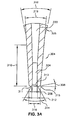
- FIGS. 3A and 3B are detailed sectional views of working tip 304 according to another exemplary embodiment of the present invention.
- the cylindrical body portion, tapered portion and axial passage of the bonding tool in this exemplary embodiment are essential identical to that of the first exemplary embodiment descriptions related thereto are not repeated.
- working tip 304 has a working face 311 forming, i.e., an outer annular chamfer having a face angle 308 of between 8 and 15 degrees.
- face angle 308 is between about 10 and 12 degrees and preferably 11 degrees.
- Adjacent outer annular chamfer 311 is inner annular chamfer 313 having an overall angle 314 of less than 90 degrees.
- chamfer angle 314 is between 60 and 90 degrees, and most preferably about 60 degrees.
- annular chamfer 313 has a width of between 1 and 3 microns.
- Cylindrical passage 324 is coupled between the upper portion of chamfer 313 and axial passage 220 .
- cylindrical passage 324 has a diameter 306 of between about 14 and 16 microns and preferably about 15 microns to accommodate a bonding wire (not shown), chamfer 313 has an outer diameter 312 of between about 17 and 19 microns and preferably about 18 microns, and working tip 304 has a outer diameter 316 of between about 37 and 39 microns, and preferably about 38 microns. Diameter 306 of cylindrical passage 324 may be determined based on the diameter of the bonding wire plus 2 microns. Further, as shown in FIG.
- working tip 304 has a substantially constant taper 319 of between about 0 and 10 degrees and preferably about 7 degrees to avoid contact of adjacent bonding wires by bonding tool 200 , and a length 310 of between about 117 and 137 microns. In a preferred embodiment length 310 is about 127 microns.
- Providing a bonding tool such as that described above is merely half the battle in meeting the needs of the semiconductor industry. It is important to be able to form the bonding tool form a material that is sufficiently strong to withstand the forces exerted on the tool during the bonding process, yet resilient enough to flex as needed without breaking.
- the inventors have determined that by forming the bonding tool from at least 80% Zirconia (ZrO 2 ) by weight these needs are met.
- Yttria stabilized Zirconia is used to form the bonding tool.
- about 95% by weight of Zirconia is combined with about 5% by weight of Y 2 O 3 .
- the inventors have determined that pure Zirconia undergoes a phase transformation process during heat treatment. Pure Zirconia is monoclinic at room temperature and changes to a denser tetragonal form at about 1000 C. This involves a large volume change and creates cracks within its structures during the sintering process at a temperature of between about 1350 and 1500° C.
- Y 2 O 3 create a mixture of the cubic phase and the monoclinic phase at low temperatures, such as less than 900° C.
- This phase transformation process that takes place with the presence of the cubic phase and involves with much less volume change, which, in turn, reduces the thermal stresses and minimizes the formation of microcracks.
- This material has a much higher bending strength than conventional Alumina based materials, and, as a result, improves the manufacturing capabilities of the bonding tool.
- up to 20% AL 2 O 3 by weight is added to the Yttria stabilized Zirconia.
- This material has an acoustic behavior similar to that of conventional Alumina based materials.
Landscapes
- Engineering & Computer Science (AREA)
- Computer Hardware Design (AREA)
- Microelectronics & Electronic Packaging (AREA)
- Power Engineering (AREA)
- Manufacturing & Machinery (AREA)
- Mechanical Engineering (AREA)
- Physics & Mathematics (AREA)
- Condensed Matter Physics & Semiconductors (AREA)
- General Physics & Mathematics (AREA)
- Wire Bonding (AREA)
Priority Applications (10)
| Application Number | Priority Date | Filing Date | Title |
|---|---|---|---|
| US09/907,191 US6715658B2 (en) | 2001-07-17 | 2001-07-17 | Ultra fine pitch capillary |
| MYPI20021172A MY122909A (en) | 2001-07-17 | 2002-04-01 | Ultra fine pitch capillary |
| TW91107086A TW558778B (en) | 2001-07-17 | 2002-04-09 | Ultra fine pitch capillary |
| JP2003514584A JP2004536456A (ja) | 2001-07-17 | 2002-05-29 | 極細ピッチキャピラリー |
| PCT/US2002/016663 WO2003009335A2 (en) | 2001-07-17 | 2002-05-29 | Ultra fine pitch capillary |
| KR10-2003-7016055A KR20040017226A (ko) | 2001-07-17 | 2002-05-29 | 초미세 피치 캐필러리 |
| CNA02814080XA CN1528008A (zh) | 2001-07-17 | 2002-05-29 | 超小间距毛细管 |
| EP20020731946 EP1393353A2 (en) | 2001-07-17 | 2002-05-29 | Ultra fine pitch capillary |
| US10/639,302 US6910612B2 (en) | 2001-07-17 | 2003-08-12 | Capillary with contained inner chamfer |
| US11/037,431 US7004369B2 (en) | 2001-07-17 | 2005-01-18 | Capillary with contained inner chamfer |
Applications Claiming Priority (1)
| Application Number | Priority Date | Filing Date | Title |
|---|---|---|---|
| US09/907,191 US6715658B2 (en) | 2001-07-17 | 2001-07-17 | Ultra fine pitch capillary |
Related Child Applications (1)
| Application Number | Title | Priority Date | Filing Date |
|---|---|---|---|
| US10/639,302 Continuation-In-Part US6910612B2 (en) | 2001-07-17 | 2003-08-12 | Capillary with contained inner chamfer |
Publications (2)
| Publication Number | Publication Date |
|---|---|
| US20030015567A1 US20030015567A1 (en) | 2003-01-23 |
| US6715658B2 true US6715658B2 (en) | 2004-04-06 |
Family
ID=25423667
Family Applications (1)
| Application Number | Title | Priority Date | Filing Date |
|---|---|---|---|
| US09/907,191 Expired - Fee Related US6715658B2 (en) | 2001-07-17 | 2001-07-17 | Ultra fine pitch capillary |
Country Status (8)
| Country | Link |
|---|---|
| US (1) | US6715658B2 (ja) |
| EP (1) | EP1393353A2 (ja) |
| JP (1) | JP2004536456A (ja) |
| KR (1) | KR20040017226A (ja) |
| CN (1) | CN1528008A (ja) |
| MY (1) | MY122909A (ja) |
| TW (1) | TW558778B (ja) |
| WO (1) | WO2003009335A2 (ja) |
Cited By (12)
| Publication number | Priority date | Publication date | Assignee | Title |
|---|---|---|---|---|
| US20040041000A1 (en) * | 2002-08-29 | 2004-03-04 | Rohm Co., Ltd. | Capillary for wire bonding and method of wire bonding using it |
| US20040094606A1 (en) * | 2001-07-17 | 2004-05-20 | Gil Perlberg | Capillary with contained inner chamfer |
| US20050252950A1 (en) * | 2004-05-12 | 2005-11-17 | Kulicke And Soffa Investments, Inc. | Low-profile capillary for wire bonding |
| US20070085008A1 (en) * | 2005-10-13 | 2007-04-19 | Seagate Technology Llc | Ceramic corona discharge emitter tip |
| US20080073406A1 (en) * | 2003-12-04 | 2008-03-27 | Dan Mironescu | Multi-part capillary |
| US20080314963A1 (en) * | 2006-07-03 | 2008-12-25 | Kulicke And Soffa Industries, Inc. | Bonding Tool With Improved Finish |
| US9543267B2 (en) | 2013-01-22 | 2017-01-10 | Micro Point Pro LTD. | Ultra fine pitch wedge for thicker wire |
| USD797171S1 (en) * | 2015-02-03 | 2017-09-12 | Coorstek, Inc. | Ceramic bonding tool with textured tip |
| USD797172S1 (en) * | 2015-02-03 | 2017-09-12 | Coorstek, Inc. | Ceramic bonding tool with textured tip |
| USD797826S1 (en) * | 2015-02-03 | 2017-09-19 | Coorstek, Inc. | Ceramic bonding tool with textured tip |
| US9931709B2 (en) | 2016-01-26 | 2018-04-03 | Orthodyne Electronics Corporation | Wedge bonding tools, wedge bonding systems, and related methods |
| USD868123S1 (en) | 2016-12-20 | 2019-11-26 | Coorstek, Inc. | Wire bonding wedge tool |
Families Citing this family (6)
| Publication number | Priority date | Publication date | Assignee | Title |
|---|---|---|---|---|
| KR100642071B1 (ko) * | 2005-03-03 | 2006-11-10 | 이정구 | 개선된 보틀 넥을 갖는 미세피치 본딩용 캐필러리 및 그 제조방법 |
| KR100718889B1 (ko) * | 2005-11-28 | 2007-05-16 | 이정구 | 투스텝 하이 보틀넥을 갖는 와이어 본딩 캐필러리 |
| CN102522349B (zh) * | 2011-12-13 | 2014-08-27 | 三星半导体(中国)研究开发有限公司 | 用于引线键合的劈刀 |
| CN102637613B (zh) * | 2012-05-09 | 2015-07-01 | 四川立泰电子有限公司 | 一种粗铝丝引线键合的实现方法 |
| US9093515B2 (en) | 2013-07-17 | 2015-07-28 | Freescale Semiconductor, Inc. | Wire bonding capillary with working tip protrusion |
| JP6064308B2 (ja) * | 2015-07-03 | 2017-01-25 | Toto株式会社 | ボンディングキャピラリ |
Citations (33)
| Publication number | Priority date | Publication date | Assignee | Title |
|---|---|---|---|---|
| US3917148A (en) * | 1973-10-19 | 1975-11-04 | Technical Devices Inc | Welding tip |
| US3971499A (en) * | 1974-09-03 | 1976-07-27 | Tribotech | Bonding tool |
| US4405074A (en) * | 1981-08-31 | 1983-09-20 | Kulicke And Soffa Industries Inc. | Composite bonding tool and method of making same |
| JPS63239959A (ja) * | 1987-03-27 | 1988-10-05 | Toshiba Corp | ワイヤボンデイング用キヤピラリ |
| US4821944A (en) | 1988-02-08 | 1989-04-18 | Mitsubishi Denki Kabushiki Kaisha | Method for bonding a wire and bonding apparatus |
| US4974767A (en) * | 1988-04-25 | 1990-12-04 | Texas Instruments Incorporated | Double cone wire bonding capillary |
| JPH04149065A (ja) * | 1990-10-12 | 1992-05-22 | Toshiba Corp | ボンディングキャピラリおよび光コネクタ用部品 |
| EP0622149A1 (en) | 1993-04-30 | 1994-11-02 | Matsushita Electric Industrial Co., Ltd. | A capillary for a wire bonding apparatus and a method for forming an electric connection bump using the capillary |
| US5421503A (en) * | 1994-08-24 | 1995-06-06 | Kulicke And Soffa Investments, Inc. | Fine pitch capillary bonding tool |
| US5437405A (en) * | 1994-08-22 | 1995-08-01 | National Semiconductor Corporation | Method and apparatus for stitch bonding of wires to integrated circuit bonding pads |
| US5465899A (en) | 1994-10-14 | 1995-11-14 | Texas Instruments Incorporated | Method and apparatus for fine pitch wire bonding using a shaved capillary |
| US5558270A (en) * | 1995-01-06 | 1996-09-24 | Kulicke And Soffa Investments, Inc | Fine pitch capillary/wedge bonding tool |
| JPH09162223A (ja) * | 1995-12-08 | 1997-06-20 | Can Electron:Kk | ワイヤーボンディングキャピラリー |
| US5662261A (en) * | 1995-04-11 | 1997-09-02 | Micron Technology, Inc. | Wire bonding capillary |
| EP0834919A2 (en) | 1996-10-01 | 1998-04-08 | Matsushita Electric Industrial Co., Ltd. | Semiconductor element having a bump electrode |
| WO1998049121A1 (fr) | 1997-04-25 | 1998-11-05 | Kyocera Corporation | Agglomere de zircone semiconducteur et element eliminateur d'electricite statique comprenant un agglomere de zircone semiconducteur |
| US5871141A (en) * | 1997-05-22 | 1999-02-16 | Kulicke And Soffa, Investments, Inc. | Fine pitch bonding tool for constrained bonding |
| US5906308A (en) | 1996-08-21 | 1999-05-25 | Kabushiki Kaisha Shinkawa | Capillary for use in a wire bonding apparatus |
| JPH11186315A (ja) * | 1997-12-19 | 1999-07-09 | Hitachi Ltd | ワイヤボンディング装置及びそれを用いた半導体装置の製造方法 |
| US5931368A (en) * | 1997-03-28 | 1999-08-03 | Kulicke And Soffa Investments, Inc | Long life bonding tool |
| JPH11251357A (ja) * | 1998-03-06 | 1999-09-17 | Hitachi Ltd | ワイヤボンディング方法および装置 |
| US5954260A (en) | 1996-12-17 | 1999-09-21 | Texas Instruments Incorporated | Fine pitch bonding technique |
| US5984162A (en) * | 1996-02-26 | 1999-11-16 | Texas Instruments Incorporated | Room temperature ball bonding |
| US6065667A (en) | 1997-01-15 | 2000-05-23 | National Semiconductor Corporation | Method and apparatus for fine pitch wire bonding |
| US6155474A (en) | 1997-12-16 | 2000-12-05 | Texas Instruments Incorporated | Fine pitch bonding technique |
| US6213378B1 (en) | 1997-01-15 | 2001-04-10 | National Semiconductor Corporation | Method and apparatus for ultra-fine pitch wire bonding |
| KR20010068181A (ko) * | 2000-04-17 | 2001-07-23 | 이강열 | 와이어 본딩용 캐필러리 소결제, 이를 이용한 와이어본딩용 캐필러리 소결체의 제조 방법 및 이를 적용한와이어 본딩용 캐필러리 제조 방법 |
| US20010045443A1 (en) * | 2000-04-28 | 2001-11-29 | Amir Miller | Controlled attenuation capillary |
| US6325269B1 (en) * | 1997-12-19 | 2001-12-04 | Toto Ltd. | Wire bonding capillary |
| US6354479B1 (en) * | 1999-02-25 | 2002-03-12 | Sjm Technologies | Dissipative ceramic bonding tip |
| US20020033408A1 (en) * | 2000-04-28 | 2002-03-21 | Amir Miller | Controlled attenuation capillary with planar surface |
| US20020096551A1 (en) * | 1999-02-25 | 2002-07-25 | Reiber Steven Frederick | Dissipative ceramic bonding tool tip |
| US20020158374A1 (en) * | 2001-02-28 | 2002-10-31 | Billiet Romain L. | Ultrasmall semiconductor bonding tools and method of fabrication thereof |
-
2001
- 2001-07-17 US US09/907,191 patent/US6715658B2/en not_active Expired - Fee Related
-
2002
- 2002-04-01 MY MYPI20021172A patent/MY122909A/en unknown
- 2002-04-09 TW TW91107086A patent/TW558778B/zh not_active IP Right Cessation
- 2002-05-29 CN CNA02814080XA patent/CN1528008A/zh active Pending
- 2002-05-29 EP EP20020731946 patent/EP1393353A2/en not_active Withdrawn
- 2002-05-29 KR KR10-2003-7016055A patent/KR20040017226A/ko not_active Application Discontinuation
- 2002-05-29 WO PCT/US2002/016663 patent/WO2003009335A2/en not_active Application Discontinuation
- 2002-05-29 JP JP2003514584A patent/JP2004536456A/ja active Pending
Patent Citations (35)
| Publication number | Priority date | Publication date | Assignee | Title |
|---|---|---|---|---|
| US3917148A (en) * | 1973-10-19 | 1975-11-04 | Technical Devices Inc | Welding tip |
| US3971499A (en) * | 1974-09-03 | 1976-07-27 | Tribotech | Bonding tool |
| US4405074A (en) * | 1981-08-31 | 1983-09-20 | Kulicke And Soffa Industries Inc. | Composite bonding tool and method of making same |
| JPS63239959A (ja) * | 1987-03-27 | 1988-10-05 | Toshiba Corp | ワイヤボンデイング用キヤピラリ |
| US4821944A (en) | 1988-02-08 | 1989-04-18 | Mitsubishi Denki Kabushiki Kaisha | Method for bonding a wire and bonding apparatus |
| US4974767A (en) * | 1988-04-25 | 1990-12-04 | Texas Instruments Incorporated | Double cone wire bonding capillary |
| JPH04149065A (ja) * | 1990-10-12 | 1992-05-22 | Toshiba Corp | ボンディングキャピラリおよび光コネクタ用部品 |
| EP0622149A1 (en) | 1993-04-30 | 1994-11-02 | Matsushita Electric Industrial Co., Ltd. | A capillary for a wire bonding apparatus and a method for forming an electric connection bump using the capillary |
| US5437405A (en) * | 1994-08-22 | 1995-08-01 | National Semiconductor Corporation | Method and apparatus for stitch bonding of wires to integrated circuit bonding pads |
| US5421503A (en) * | 1994-08-24 | 1995-06-06 | Kulicke And Soffa Investments, Inc. | Fine pitch capillary bonding tool |
| US5465899A (en) | 1994-10-14 | 1995-11-14 | Texas Instruments Incorporated | Method and apparatus for fine pitch wire bonding using a shaved capillary |
| US5558270A (en) * | 1995-01-06 | 1996-09-24 | Kulicke And Soffa Investments, Inc | Fine pitch capillary/wedge bonding tool |
| US5662261A (en) * | 1995-04-11 | 1997-09-02 | Micron Technology, Inc. | Wire bonding capillary |
| JPH09162223A (ja) * | 1995-12-08 | 1997-06-20 | Can Electron:Kk | ワイヤーボンディングキャピラリー |
| US5984162A (en) * | 1996-02-26 | 1999-11-16 | Texas Instruments Incorporated | Room temperature ball bonding |
| US5906308A (en) | 1996-08-21 | 1999-05-25 | Kabushiki Kaisha Shinkawa | Capillary for use in a wire bonding apparatus |
| EP0834919A2 (en) | 1996-10-01 | 1998-04-08 | Matsushita Electric Industrial Co., Ltd. | Semiconductor element having a bump electrode |
| US20010005054A1 (en) * | 1996-10-01 | 2001-06-28 | Kazushi Higashi | Method of forming a ball bond using a bonding capillary |
| US5954260A (en) | 1996-12-17 | 1999-09-21 | Texas Instruments Incorporated | Fine pitch bonding technique |
| US6213378B1 (en) | 1997-01-15 | 2001-04-10 | National Semiconductor Corporation | Method and apparatus for ultra-fine pitch wire bonding |
| US6065667A (en) | 1997-01-15 | 2000-05-23 | National Semiconductor Corporation | Method and apparatus for fine pitch wire bonding |
| US5931368A (en) * | 1997-03-28 | 1999-08-03 | Kulicke And Soffa Investments, Inc | Long life bonding tool |
| WO1998049121A1 (fr) | 1997-04-25 | 1998-11-05 | Kyocera Corporation | Agglomere de zircone semiconducteur et element eliminateur d'electricite statique comprenant un agglomere de zircone semiconducteur |
| US20020010069A1 (en) | 1997-04-25 | 2002-01-24 | Kyocera Corperation | Semiconductive zirconia sintering body and electrostatic removing member constructed by semiconductive zirconia sintering body |
| US5871141A (en) * | 1997-05-22 | 1999-02-16 | Kulicke And Soffa, Investments, Inc. | Fine pitch bonding tool for constrained bonding |
| US6155474A (en) | 1997-12-16 | 2000-12-05 | Texas Instruments Incorporated | Fine pitch bonding technique |
| US6325269B1 (en) * | 1997-12-19 | 2001-12-04 | Toto Ltd. | Wire bonding capillary |
| JPH11186315A (ja) * | 1997-12-19 | 1999-07-09 | Hitachi Ltd | ワイヤボンディング装置及びそれを用いた半導体装置の製造方法 |
| JPH11251357A (ja) * | 1998-03-06 | 1999-09-17 | Hitachi Ltd | ワイヤボンディング方法および装置 |
| US6354479B1 (en) * | 1999-02-25 | 2002-03-12 | Sjm Technologies | Dissipative ceramic bonding tip |
| US20020096551A1 (en) * | 1999-02-25 | 2002-07-25 | Reiber Steven Frederick | Dissipative ceramic bonding tool tip |
| KR20010068181A (ko) * | 2000-04-17 | 2001-07-23 | 이강열 | 와이어 본딩용 캐필러리 소결제, 이를 이용한 와이어본딩용 캐필러리 소결체의 제조 방법 및 이를 적용한와이어 본딩용 캐필러리 제조 방법 |
| US20010045443A1 (en) * | 2000-04-28 | 2001-11-29 | Amir Miller | Controlled attenuation capillary |
| US20020033408A1 (en) * | 2000-04-28 | 2002-03-21 | Amir Miller | Controlled attenuation capillary with planar surface |
| US20020158374A1 (en) * | 2001-02-28 | 2002-10-31 | Billiet Romain L. | Ultrasmall semiconductor bonding tools and method of fabrication thereof |
Non-Patent Citations (1)
| Title |
|---|
| International Search Report dated Feb. 28, 2003, application No. PCT/US 02/16663. |
Cited By (25)
| Publication number | Priority date | Publication date | Assignee | Title |
|---|---|---|---|---|
| US20040094606A1 (en) * | 2001-07-17 | 2004-05-20 | Gil Perlberg | Capillary with contained inner chamfer |
| US20050121494A1 (en) * | 2001-07-17 | 2005-06-09 | Gil Perlberg | Capillary with contained inner chamfer |
| US6910612B2 (en) * | 2001-07-17 | 2005-06-28 | Kulicke & Soffa Investments, Inc. | Capillary with contained inner chamfer |
| US7004369B2 (en) * | 2001-07-17 | 2006-02-28 | Kulicke & Soffa Investments, Inc. | Capillary with contained inner chamfer |
| US7051915B2 (en) * | 2002-08-29 | 2006-05-30 | Rohm Co., Ltd. | Capillary for wire bonding and method of wire bonding using it |
| US20040041000A1 (en) * | 2002-08-29 | 2004-03-04 | Rohm Co., Ltd. | Capillary for wire bonding and method of wire bonding using it |
| US7500590B2 (en) * | 2003-12-04 | 2009-03-10 | Kulicke And Soffa Industries, Inc. | Multi-part capillary |
| US20080073406A1 (en) * | 2003-12-04 | 2008-03-27 | Dan Mironescu | Multi-part capillary |
| US7320425B2 (en) | 2004-05-12 | 2008-01-22 | Kulicke And Soffa Industries, Inc. | Low-profile capillary for wire bonding |
| US20080210740A1 (en) * | 2004-05-12 | 2008-09-04 | Kulicke And Soffa Industries, Inc. | Low-profile capillary for wire bonding |
| US20050252950A1 (en) * | 2004-05-12 | 2005-11-17 | Kulicke And Soffa Investments, Inc. | Low-profile capillary for wire bonding |
| US7500591B2 (en) | 2004-05-12 | 2009-03-10 | Kulicke And Soffa Industries, Inc. | Low-profile capillary for wire bonding |
| US20070085008A1 (en) * | 2005-10-13 | 2007-04-19 | Seagate Technology Llc | Ceramic corona discharge emitter tip |
| US20080314963A1 (en) * | 2006-07-03 | 2008-12-25 | Kulicke And Soffa Industries, Inc. | Bonding Tool With Improved Finish |
| US9543267B2 (en) | 2013-01-22 | 2017-01-10 | Micro Point Pro LTD. | Ultra fine pitch wedge for thicker wire |
| USD797171S1 (en) * | 2015-02-03 | 2017-09-12 | Coorstek, Inc. | Ceramic bonding tool with textured tip |
| USD797172S1 (en) * | 2015-02-03 | 2017-09-12 | Coorstek, Inc. | Ceramic bonding tool with textured tip |
| USD797826S1 (en) * | 2015-02-03 | 2017-09-19 | Coorstek, Inc. | Ceramic bonding tool with textured tip |
| USD821468S1 (en) | 2015-02-03 | 2018-06-26 | Coorstek, Inc. | Ceramic bonding tool with textured tip |
| USD824969S1 (en) | 2015-02-03 | 2018-08-07 | Coorstek, Inc. | Ceramic bonding tool with textured tip |
| USD824970S1 (en) | 2015-02-03 | 2018-08-07 | Coorstek, Inc. | Ceramic bonding tool with textured tip |
| US9931709B2 (en) | 2016-01-26 | 2018-04-03 | Orthodyne Electronics Corporation | Wedge bonding tools, wedge bonding systems, and related methods |
| US10449627B2 (en) | 2016-01-26 | 2019-10-22 | Kulicke And Soffa Industries, Inc. | Wedge bonding tools, wedge bonding systems, and related methods |
| US10987753B2 (en) | 2016-01-26 | 2021-04-27 | Kulicke And Soffa Industries, Inc. | Wedge bonding tools, wedge bonding systems, and related methods |
| USD868123S1 (en) | 2016-12-20 | 2019-11-26 | Coorstek, Inc. | Wire bonding wedge tool |
Also Published As
| Publication number | Publication date |
|---|---|
| CN1528008A (zh) | 2004-09-08 |
| MY122909A (en) | 2006-05-31 |
| WO2003009335A3 (en) | 2003-04-10 |
| US20030015567A1 (en) | 2003-01-23 |
| EP1393353A2 (en) | 2004-03-03 |
| KR20040017226A (ko) | 2004-02-26 |
| TW558778B (en) | 2003-10-21 |
| WO2003009335A2 (en) | 2003-01-30 |
| JP2004536456A (ja) | 2004-12-02 |
Similar Documents
| Publication | Publication Date | Title |
|---|---|---|
| US7004369B2 (en) | Capillary with contained inner chamfer | |
| US6715658B2 (en) | Ultra fine pitch capillary | |
| US7500590B2 (en) | Multi-part capillary | |
| US5544804A (en) | Capillary designs and process for fine pitch ball bonding | |
| US20080314963A1 (en) | Bonding Tool With Improved Finish | |
| EP1381489B1 (en) | Controlled attenuation capillary | |
| KR20060048506A (ko) | 와이어 본딩용 모세관 | |
| US6497356B2 (en) | Controlled attenuation capillary with planar surface | |
| US20090308911A1 (en) | Wire bonding capillary tool having multiple outer steps | |
| KR100792124B1 (ko) | 효율적인 에너지 전달 캐필러리 | |
| EP2167269B1 (en) | Wire bonding capillary tool having multiple outer steps | |
| JPS62256447A (ja) | ワイヤボンデイング用キヤピラリチツプ | |
| JPH03171743A (ja) | 半導体装置の製造方法 |
Legal Events
| Date | Code | Title | Description |
|---|---|---|---|
| AS | Assignment |
Owner name: KULICKE & SOFFA INVESTEMENTS, INC., DELAWARE Free format text: ASSIGNMENT OF ASSIGNORS INTEREST;ASSIGNORS:PERLBERG, GIL;ATZMON, ZIV;SONNENREICH, BENJAMIN;AND OTHERS;REEL/FRAME:012468/0461;SIGNING DATES FROM 20011028 TO 20011107 |
|
| CC | Certificate of correction | ||
| AS | Assignment |
Owner name: KULICKE AND SOFFA INDUSTRIES, INC., PENNSYLVANIA Free format text: MERGER;ASSIGNOR:KULICKE & SOFFA INVESTMENTS, INC.;REEL/FRAME:018323/0096 Effective date: 20051021 |
|
| REMI | Maintenance fee reminder mailed | ||
| LAPS | Lapse for failure to pay maintenance fees | ||
| STCH | Information on status: patent discontinuation |
Free format text: PATENT EXPIRED DUE TO NONPAYMENT OF MAINTENANCE FEES UNDER 37 CFR 1.362 |
|
| FP | Lapsed due to failure to pay maintenance fee |
Effective date: 20080406 |