US6699594B1 - Organic electroluminescent device - Google Patents
Organic electroluminescent device Download PDFInfo
- Publication number
- US6699594B1 US6699594B1 US09/675,166 US67516600A US6699594B1 US 6699594 B1 US6699594 B1 US 6699594B1 US 67516600 A US67516600 A US 67516600A US 6699594 B1 US6699594 B1 US 6699594B1
- Authority
- US
- United States
- Prior art keywords
- group
- substituted
- formula
- substituents
- compound expressed
- Prior art date
- Legal status (The legal status is an assumption and is not a legal conclusion. Google has not performed a legal analysis and makes no representation as to the accuracy of the status listed.)
- Expired - Lifetime, expires
Links
Images


Classifications
-
- H—ELECTRICITY
- H10—SEMICONDUCTOR DEVICES; ELECTRIC SOLID-STATE DEVICES NOT OTHERWISE PROVIDED FOR
- H10K—ORGANIC ELECTRIC SOLID-STATE DEVICES
- H10K85/00—Organic materials used in the body or electrodes of devices covered by this subclass
- H10K85/60—Organic compounds having low molecular weight
- H10K85/615—Polycyclic condensed aromatic hydrocarbons, e.g. anthracene
- H10K85/624—Polycyclic condensed aromatic hydrocarbons, e.g. anthracene containing six or more rings
-
- H—ELECTRICITY
- H10—SEMICONDUCTOR DEVICES; ELECTRIC SOLID-STATE DEVICES NOT OTHERWISE PROVIDED FOR
- H10K—ORGANIC ELECTRIC SOLID-STATE DEVICES
- H10K85/00—Organic materials used in the body or electrodes of devices covered by this subclass
- H10K85/60—Organic compounds having low molecular weight
- H10K85/631—Amine compounds having at least two aryl rest on at least one amine-nitrogen atom, e.g. triphenylamine
- H10K85/633—Amine compounds having at least two aryl rest on at least one amine-nitrogen atom, e.g. triphenylamine comprising polycyclic condensed aromatic hydrocarbons as substituents on the nitrogen atom
-
- H—ELECTRICITY
- H10—SEMICONDUCTOR DEVICES; ELECTRIC SOLID-STATE DEVICES NOT OTHERWISE PROVIDED FOR
- H10K—ORGANIC ELECTRIC SOLID-STATE DEVICES
- H10K50/00—Organic light-emitting devices
- H10K50/10—OLEDs or polymer light-emitting diodes [PLED]
- H10K50/11—OLEDs or polymer light-emitting diodes [PLED] characterised by the electroluminescent [EL] layers
-
- H—ELECTRICITY
- H10—SEMICONDUCTOR DEVICES; ELECTRIC SOLID-STATE DEVICES NOT OTHERWISE PROVIDED FOR
- H10K—ORGANIC ELECTRIC SOLID-STATE DEVICES
- H10K85/00—Organic materials used in the body or electrodes of devices covered by this subclass
- H10K85/30—Coordination compounds
-
- H—ELECTRICITY
- H10—SEMICONDUCTOR DEVICES; ELECTRIC SOLID-STATE DEVICES NOT OTHERWISE PROVIDED FOR
- H10K—ORGANIC ELECTRIC SOLID-STATE DEVICES
- H10K85/00—Organic materials used in the body or electrodes of devices covered by this subclass
- H10K85/30—Coordination compounds
- H10K85/321—Metal complexes comprising a group IIIA element, e.g. Tris (8-hydroxyquinoline) gallium [Gaq3]
- H10K85/324—Metal complexes comprising a group IIIA element, e.g. Tris (8-hydroxyquinoline) gallium [Gaq3] comprising aluminium, e.g. Alq3
-
- H—ELECTRICITY
- H10—SEMICONDUCTOR DEVICES; ELECTRIC SOLID-STATE DEVICES NOT OTHERWISE PROVIDED FOR
- H10K—ORGANIC ELECTRIC SOLID-STATE DEVICES
- H10K85/00—Organic materials used in the body or electrodes of devices covered by this subclass
- H10K85/60—Organic compounds having low molecular weight
- H10K85/615—Polycyclic condensed aromatic hydrocarbons, e.g. anthracene
- H10K85/623—Polycyclic condensed aromatic hydrocarbons, e.g. anthracene containing five rings, e.g. pentacene
-
- H—ELECTRICITY
- H10—SEMICONDUCTOR DEVICES; ELECTRIC SOLID-STATE DEVICES NOT OTHERWISE PROVIDED FOR
- H10K—ORGANIC ELECTRIC SOLID-STATE DEVICES
- H10K85/00—Organic materials used in the body or electrodes of devices covered by this subclass
- H10K85/60—Organic compounds having low molecular weight
- H10K85/649—Aromatic compounds comprising a hetero atom
- H10K85/654—Aromatic compounds comprising a hetero atom comprising only nitrogen as heteroatom
-
- H—ELECTRICITY
- H10—SEMICONDUCTOR DEVICES; ELECTRIC SOLID-STATE DEVICES NOT OTHERWISE PROVIDED FOR
- H10K—ORGANIC ELECTRIC SOLID-STATE DEVICES
- H10K85/00—Organic materials used in the body or electrodes of devices covered by this subclass
- H10K85/60—Organic compounds having low molecular weight
- H10K85/649—Aromatic compounds comprising a hetero atom
- H10K85/656—Aromatic compounds comprising a hetero atom comprising two or more different heteroatoms per ring
- H10K85/6565—Oxadiazole compounds
-
- Y—GENERAL TAGGING OF NEW TECHNOLOGICAL DEVELOPMENTS; GENERAL TAGGING OF CROSS-SECTIONAL TECHNOLOGIES SPANNING OVER SEVERAL SECTIONS OF THE IPC; TECHNICAL SUBJECTS COVERED BY FORMER USPC CROSS-REFERENCE ART COLLECTIONS [XRACs] AND DIGESTS
- Y10—TECHNICAL SUBJECTS COVERED BY FORMER USPC
- Y10S—TECHNICAL SUBJECTS COVERED BY FORMER USPC CROSS-REFERENCE ART COLLECTIONS [XRACs] AND DIGESTS
- Y10S428/00—Stock material or miscellaneous articles
- Y10S428/917—Electroluminescent
Definitions
- the present invention relates to an organic electroluminescent device having an excellent luminance property such as high luminance efficiency.
- organic electroluminescent device (which will hereinafter be called “organic EL device”) is a light-emitting device which makes use of the principle that when an electric field is applied, a fluorescent material emits light in response to the charge recombination of holes injected from an anode and electrons injected from a cathode.
- an organic EL device using tris(8-hydroxyquinolinol aluminum) in a light-emitting layer and a triphenyldiamine derivative in a hole-transporting layer.
- This stacked structure gives such advantages as an improvement in the injection efficiency of holes into the light-emitting layer; and confinement of the excitons into the light-emitting layer.
- a double layered structure composed of a hole-injecting and transporting layer and an electron-transporting and light-emitting layer or a triple layered structure composed of a hole-injecting and transporting layer, a light-emitting layer and an electron-injecting and transporting layer is well known as an organic EL device.
- various improvements in the device structure or fabrication process have been introduced to such multi-layered devices.
- triphenyl amine derivatives and aromatic diamine derivatives such as 4,4′, 4′′-tris(3-methylphenylphenylamino)-triphenyl amine which is a star burst molecule and N,N′-diphenyl-N,N′-bis(3-methylphenyl)-[1,1′-biphenyl]-4,4′-diamine are well known (for example, Patent Publications JP-A-8-20771, JP-A-8-40995, JP-A-8-40997, JP-A-8-53397, and JP-A-8-87122).
- oxadiazole derivatives, triazole derivatives and the like are well known.
- Chelate complexes such as tris(8-quinolinolate)aluminum complex, coumarin derivatives, tetraphenylbutadiene derivatives, bisstyrylarylene derivatives, oxadiazole derivatives and the like are known as light emitting materials. Since various color lights in a visible region from blue to red are obtained from these light-emitting materials, there is increased expectation for industrialization of a full color organic EL device (refer to, e.g., JP-A-8-239655, JP-A-7-138561, and JP-A-3-200289).
- an organic EL device having a specific one of pentacene compounds and of dibenzoperylene compounds as a luminescent material has much higher luminance than a conventional EL device.
- the material has been found to have a high carrier transporting ability, and an organic EL device prepared by employing the above material as a hole transporting material or an electron transporting material and another organic EL device prepared by employing a mixed thin film comprising the material and another hole transporting material or electron transporting material has been found to have higher luminance than the conventional one.
- an organic EL device prepared by employing, as a luminescent material, a hole transporting material or an electron transporting material, a pentacene compound and/or a dibenzoperylene compound, among the above pentacene and dibenzoperylene compounds, having a diarylamino group as a substituent exhibits an especially high luminance.
- an organic EL device prepared by employing, as a luminescent material, a hole transporting material or an electron transporting material, a pentacene compound and/or a dibenzoperylene compound, among the above pentacene and dibenzoperylene compounds, having a styryl group as an aryl group exhibits an especially high luminance.
- the present invention is based on these findings.
- the present invention provides, in a first aspect thereof, an organic electroluminescent device comprising an anode, a cathode, and one or more organic thin film layers disposed between said anode and said cathode, at least one of said layers containing, in a form of a mixture or a single substance, a pentacene compound expressed in Formula 1.
- each of R 1 to R 14 independently represents a hydrogen atom, a halogen atom, a hydroxyl group, a substituted or non-substituted amino group, nitro group or cyano group, a substituted or non-substituted alkyl group, a substituted or non-substituted alkenyl group, a substituted or non-substituted cycloalkyl group, a substituted or non-substituted alkoxyl group, a substituted or non-substituted aromatic hydrocarbon group, a substituted or non-substituted aromatic heterocyclic group, a substituted or non-substituted aralkyl group, a substituted or non-substituted aryloxy group, a substituted or non-substituted alkoxylcarbonyl group, or a carboxyl group.
- R 1 to R 14 may form a ring between two of them.
- At least one of R 1 to R 14 is a diarylamino group expressed by —NAr 1 Ar 2 (each of Ar 1 and Ar 2 independently represents a substituted or non-substituted aryl group having 6 to 20 carbons, and at least one of these has a styryl group expressed in Formula 2 below and a ring may be formed between two of them.
- each of R 15 to R 25 independently represents a hydrogen atom, a halogen atom, a hydroxyl group, a substituted or non-substituted amino group, nitro group- or cyano group, a substituted or non-substituted alkyl group, a substituted or non-substituted alkenyl group, a substituted or non-substituted cycloalkyl group, a substituted or non-substituted alkoxyl group, a substituted or non-substituted aromatic hydrocarbon group, a substituted or non-substituted aromatic heterocyclic group, a substituted or non-substituted aralkyl group, a substituted or non-substituted aryloxy group, a substituted or non-substituted alkoxylcarbonyl group, or a carboxyl group.
- the substituents R 15 to R 25 may form a ring between two of them.
- the present invention further provides, in a second aspect thereof, an organic electroluminescent device employing a compound expressed in Formula 3 in place of that expressed in Formula 1 of the first aspects.
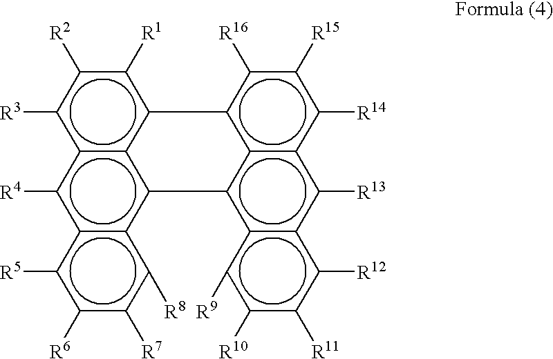
- the present invention further provides, in a third aspect thereof, an organic electroluminescent device employing a compound expressed in Formula 4 in place of that expressed in Formula 1 of the first aspect.
- the organic EL device effectively exhibits higher luminance than that obtained by a conventional organic EL device by employing the specified pentacene or dibenzopeylene compound.
- FIG. 1 is a sectional view of one example of an organic EL device in accordance with the present invention.
- FIG. 2 is a sectional view of another example of an organic EL device.
- FIG. 3 is a sectional view of a further example of an organic EL device.
- FIG. 4 is a sectional view of a still further example of an organic EL device.
- each of R 1 to R 14 and R 15 to R 25 independently represents a hydrogen atom, a halogen atom, a hydroxyl group, a substituted or non-substituted amino group, nitro group or cyano group, a substituted or non-substituted alkyl group, a substituted or non-substituted alkenyl group, a substituted or non-substituted cycloalkyl group, a substituted or non-substituted alkoxyl group, a substituted or non-substituted aromatic hydrocarbon group, a substituted or non-substituted aromatic heterocyclic group, a substituted or non-substituted aralkyl group, a substituted or non-substituted aryloxy group, a substituted or non-substituted alk
- Fluorine, chlorine, bromine and iodine may be selected as the halogen atom.
- the substituted or non-substituted amino group is expressed as —NX 1 X 2 , examples of X 1 and X 2 independently include a hydrogen atom, methyl group, ethyl group, propyl group, isopropyl group, n-butyl group, s-butyl group, isobutyl group, t-butyl group, n-pentyl group, n-hexyl group, n-heptyl group, n-octyl group, hydroxymethyl group, 1-hydroxyethyl group, 2-hydroxyethyl group, 2-hydroxyisobutyl group, 1,2-dihydroxyethyl group, 1,3-dihydroxyisopropyl group, 2,3-dihydroxy-t-butyl group, 1,2,3-trihydroxypropyl group, chloromethyl group, 1-chloroethyl group, 2-chloroethyl group, 2-chloroisobutyl group, 1,2-dichlor
- substituted or non-substituted alkyl group examples include methyl group, ethyl group, propyl group, isopropyl group, n-butyl, s-butyl, isobutyl group, t-butyl group, n-pentyl group, n-hexyl group, n-heptyl group, n-octyl group, hydroxymethyl group, 1-hydroxyethyl group, 2-hydroxyethyl group, 2-hydroxyisobutyl group, 1,2-dihydroxyethyl group, 1,3-dihydroxyisopropyl group, 2,3-dihydroxy-t-butyl group, 1,2,3-trihydroxypropyl group, chloromethyl group, 1-chloroethyl group, 2-chloroethyl group, 2-chloroisobutyl group, 1,2-chloroethyl group, 1,3-dichloroisopropyl group, 2,3-dichloro-
- Examples of the substituted or non-substituted alkenyl group include vinyl group, allyl group, 1-butenyl group, 2-butenyl group, 3-butenyl group, 1,3-butanedienyl group, 1-methylvinyl group, styryl group, 2,2-diphenylvinyl group, 1,2-diphenylvinyl group, 1-methylallyl group, 1,1-dimethylallyl group, 2-methylallyl group, 1-phenylallyl group, 2-phenylallyl group, 3-phenylallyl group, 3,3-diphenylallyl group, 1,2-dimethylallyl group, 1-phenyl-1-butenyl group and 3-phenyl-1-butenyl group.
- Examples of the substituted or non-substituted cycloalkyl group include cyclopropyl group, cyclobutyl group, cyclopentyl group, cyclohexyl group, and 4-methylcyclohexyl group.
- the substituted or non-substituted alkoxy group is represented by —OY and examples of Y include methyl group, ethyl group, propyl group, isopropyl group, n-butyl group, s-butyl group, isobutyl group, t-butyl group, n-pentyl group, n-hexyl group, n-heptyl group, n-octyl group, 18-hydroxymethyl group, 1-hydroxyethyl group, 2-hydroxyethyl group, 2-hydroxyisobutyl group, 1,2-dihydroxyethyl group, 1,3-dihydroxyisopropyl group, 2,3-dihydroxy-t-butyl group, 1,2,3-trihydroxypropyl group, chloromethyl group, 1-chloroethyl group, 2-chloroethyl group, 2-chloroisobutyl group, 1,2-dichloroethyl group, 1,3-dichloro
- Examples of the substituted or non-substituted aromatic hydrocarbon group include phenyl group, 1-naphthyl group, 2-naphthyl group, 1-anthryl group, 2-anthryl group, 9-anthryl group, 1-phenanthryl group, 2-phenanthryl group, 3-phenanthryl group, 4-phenanthryl group, 9-phenanthryl group, 1-naphthacenyl group, 2-naphthacenyl group, 9-naphthacenyl group, 1-pyrenyl group, 2-pyrenyl group, 4-pyrenyl group, 2-biphenylyl group, 3-biphenylyl group, 4-biphenylyl group, p-terphenyl-4-yl group, p-terphenyl-3-yl group, p-terphenyl-2-yl group, m-terphenyl-4-yl group, m-terphenyl-3-yl group, m-terphen
- Examples of the substituted or non-substituted aromatic heterocyclic group include 1-pyrrolyl group, 2-pyrrolyl group, 3-pyrrolyl group, pyrazinyl group, 2-pyridinyl group, 3-pyridinyl group, 4-pyridinyl group, 1-indolyl group, 2-indolyl group, 3-indolyl group, 4-indolyl group, 5-indolyl group, 6-indolyl group, 7-indolyl group, 1-isoindolyl group, 2-isoindolyl group, 3-isoindolyl group, 4-isoindolyl group, 5-isoindolyl group, 6-isoindolyl group, 7-isoindolyl group, 2-furyl group, 3-furyl group, 2-benzofuranyl group, 3-benzofuranyl group, 4-benzofuranyl group, 5-benzofuranyl group, 6-benzofuranyl group, 7-
- Examples of the substituted or non-substituted aralkyl group include benzyl group, 1-phenylethyl group, 2-phenylethyl group, 1-phenylisopropyl group, 2-phenylisopropyl group, phenyl-t-butyl group, ⁇ -naphthylmethyl group, 1- ct-naphthylethyl group, 2- ⁇ -naphthylethyl group, 1- ⁇ -naphthylisopropyl group, 2- ⁇ -naphthylisopropyl group, ⁇ -naphthylmethyl group, 1- ⁇ -naphthylethyl group, 2- ⁇ -naphthylmethyl group, 1- ⁇ -naphthylisopropyl group, 2- ⁇ -naphthylisopropyl group, 1-pyrrolylmethyl group, 2-(1-pyrrolyl)ethyl group
- the substituted or non-substituted aryloxy group is represented by —OZ, wherein Z may be phenyl group, 1-naphthyl group, 2-naphthyl group, 1-anthryl group, 2-anthryl group, 9-anthryl group, 1-phenanthryl group, 2-phenanthryl group, 3-phenanthryl group, 4-phenanthryl group, 9-phenanthryl group, 1-naphthacenyl group, 2-naphthacenyl group, 9-naphthacenyl group, 1-pyrenyl group, 2-pyrenyl group, 4-pyrenyl group, 2-biphenylyl group, 3-biphenylyl group, 4-biphenylyl group, p-terphenyl-4-yl group, p-terphenyl-3-yl group, p-terphenyl-2-yl group, m-terphenyl-4-yl group, m-terphenyl
- the substituted or non-substituted alkoxycarbonyl group is represented by —COOY, wherein Y may be methyl group, ethyl group, propyl group, isopropyl group, n-butyl group, s-butyl group, isobutyl group, t-butyl group, n-pentyl group, n-hexyl group, n-heptyl group, n-octyl group, hydroxymethyl group, 1-hydroxyethyl group, 2-hydroxyethyl group, 2-hydroxyisobutyl group, 1,2-dihydroxyethyl group, 1,3-dihydroxyisopropyl group, 2,3-dihydroxy-t-butyl group, 1,2,3-trihydroxypropyl group, chloromethyl group, 1-chloroethyl group, 2-chloroethyl group, 2-chloroisobutyl group, 1,2-dichloroethyl group, 1,3-
- bivalent groups forming a ring examples include tetramethylene group, pentamethylene group, hexamethylene group, diphenylmethan-2,2′-diyl group, diphenylethan-3,3′-diyl group and diphenylpropan-4,4′-diyl group.
- At least one of R 1 to R 14 is a diarylamino group expressed by —NAr 1 Ar 2 (each of Ar 1 and Ar 2 independently represents a substituted or non-substituted aryl group having 6 to 20 carbons wherein at least one of them has a styryl group expressed by the above Formula 2 and may form a ring.
- examples of the aryl group having 6 to 20 carbons include phenyl group, naphthyl group, anthryl group, phenanthryl group, naphthacenyl group, and pyrenyl group.
- Examples of a substituent of the aryl group include a halogen atom, hydroxyl group, the above substituted or non-substituted amino group, nitro group or cyano group, the above substituted or non-substituted alkyl group, the above substituted or non-substituted alkenyl group, the above substituted or non-substituted cycloalkyl group, the above substituted or non-substituted alkoxyl group, the above substituted or non-substituted aromatic hydrocarbon group, the above substituted or non-substituted aromatic heterocyclic group, the above substituted or non-substituted aralkyl group, the above substituted or non-substituted aryloxy group, the above substituted or non-substituted alkoxycarbonyl group and carboxyl group.
- Examples of the styryl group which Ar 1 and Ar 2 have as a substituent include non-substituted styryl group and 2,2′-diphenylvinyl group.
- the substituted styryl group having, as a substituent of a terminal phenyl group, a halogen atom, hydroxyl group, the above substituted or non-substituted amino group, nitro group or cyano group, the above substituted or non-substituted alkyl group, the above substituted or non-substituted alkenyl group, the above substituted or non-substituted cycloalkyl group, the above substituted or non-substituted alkoxyl group, the above substituted or non-substituted aromatic hydrocarbon group, the above substituted or non-substituted aromatic heterocyclic group, the above substituted or non-substituted aralkyl group, the above substituted or non-substituted
- Examples of the pentacene compounds employed in the present invention include, but not limited thereto, compounds shown in Formulae 5 to 10.
- a structure of the organic EL device of the present invention is a stacked structure having one or more organic layers between an anode and a cathode. Examples thereof are shown in FIGS. 1 to 4 .
- FIG. 1 a stacked structure consisting of an anode 12 , a luminescent layer 14 and a cathode 16 in this order stacked on a substrate 11 is illustrated.
- FIG. 2 another stacked structure consisting of an anode 12 , a hole transporting layer 13 , a luminescent layer 14 , an electron transporting layer 15 and a cathode 16 in this order stacked on a substrate 11 is illustrated.
- FIG. 1 a stacked structure consisting of an anode 12 , a hole transporting layer 13 , a luminescent layer 14 , an electron transporting layer 15 and a cathode 16 in this order stacked on a substrate 11 is illustrated.
- FIG. 3 a further stacked structure consisting of an anode 12 , a hole transporting layer 13 , a luminescent layer 14 and a cathode 16 stacked in this order on a substrate 11 is illustrated.
- FIG. 4 a still further stacked structure consisting of an anode 12 , a luminescent layer 14 , an electron transporting layer 15 and a cathode 16 stacked in this order on a substrate 11 is illustrated.
- the above-mentioned pentacene compounds may be included in any one of the organic layers, and may be doped in the hole transporting material, the luminescent material or the electron transporting material.
- the hole transporting material employed in the present invention is not especially restricted, and any compound ordinarily used as the hole transporting material can be employed.
- the hole transporting material include triphenyldiamines such as bis(di(p-tolyl)aminophenyl)-1,1-cyclohexane (Formula 11), N,N′-biphenyl-4,4′-diamine (Formula 12) and N,N′-diphenyl-N,N′-bis(1-naphthyl)-1,1′-biphenyl-4,4′-diamine (Formula 13), and star burst type molecules formulae 14 to 16).
- triphenyldiamines such as bis(di(p-tolyl)aminophenyl)-1,1-cyclohexane (Formula 11), N,N′-biphenyl-4,4′-diamine (Formula 12) and N,N′-diphenyl-
- the electron transporting material employed in the present invention is not especially restricted, and any compound ordinarily used as the electron transporting material can be employed.
- the electron transporting material include oxadiazole derivatives such as 2-(4-biphenylyl)-5-(4-t-butylphenyl)-1,3,4-oxadiazole (Formula 17) and bis[2-(4-t-butylphenyl)-1,3,4-oxadiazol]-m-phenylene (Formula 18), triazole derivatives (Formulae 19 and 20) and quinolinol-based metal complexes (Formulae 21 to 24).
- oxadiazole derivatives such as 2-(4-biphenylyl)-5-(4-t-butylphenyl)-1,3,4-oxadiazole (Formula 17) and bis[2-(4-t-butylphenyl)-1,3,4-oxadiazol]-m-phenylene (Formula 18
- the anode of the organic thin film EL device has a role of injecting holes into the hole transporting layers, and effectively has a work function of 4.5 eV or more.
- the anode material employed in the present invention include an indium oxide-tin alloy (ITO), tin oxide (NESA), gold, silver, platinum and copper.
- the cathode has a role of injecting electrons into the electron transporting layers and/or the luminescent layers, and preferably has a small work function.
- the cathode material is not especially restricted, and indium, aluminum, magnesium, a magnesium-indium alloy, a magnesium-aluminum alloy, an aluminum-lithium alloy, an aluminum-scandium-lithium alloy or a magnesium-silver alloy may be employed.
- a method of forming the respective layers of the organic EL device of the present invention is not especially restricted, and any one of known methods such as a vacuum vapor deposition method and a spin coating method may be employed.
- the organic thin film layer containing the compound expressed in Formula 1 can be formed by an application method such as a vacuum vapor deposition method, a molecular beam evaporation method (MBE method), a dipping method employing a solution prepared by dissolving the material in a solvent, a spin coating method, a casting method, a bar coating method and a roll coating method.
- the thickness of the respective organic layers of the organic device in accordance with the present invention is not especially restricted, it is ordinarily in a range between several nm and 1 micronmeter. If the thickness is excessively thin, such a defect as a pin hole is likely produced, and on the other hand if it is excessively thick, a high applied voltage is required to make its efficiency worse.
- the dibenzoperylene compounds employed in the second and third aspects of the resent invention are those having structural formulae expressed in above Formulae 3 and 4, respectively.
- each of R 1 to R 16 independently represents the same atom or substituent as that shown in connection with R 1 to R 14 and R 15 to R 25 of Formulae 1 and 2.
- at least one of R 1 to R 16 is preferably a diarylamino group expressed by —NAr 1 Ar 2
- Each of Ar 1 and Ar 2 independently represents a substituted or non-substituted aryl group having 6 to 20 carbons, and at least one of these may have a substituted or non-substituted styryl group as a substituent.
- Examples of the dibenzoperylene compounds employed in Formula 3 include, but not limited thereto, compounds shown in Formulae 25 to 30.
- dibenzoperylene compounds employed in Formula 4 include, but not limited thereto, compounds shown in Formulae 31 to 36.
- 6,1,3-dibromopentacene, 4-methyldiphenyl-amine, potassium carbonate, and copper powder were stirred in nitrobenzene for 30 hours at 200° C.
- nitrobenzene was removed by distillation in a reduced pressure ambient, and the remainder was refined in accordance with an ordinary method to obtain 6,13-bis(4-methyldiphenylamino) pentacene.
- 6,13-bis(4-methyldiphenylamino) pentacene was reacted with phosphoryl trichloride for 5 hours at 50° C. to obtain 6,13-bis(4-formyl-4′-methyldiphenylamino) pentacene.
- the reaction product was refined in accordance with an ordinary method to obtain 7-(N-p-formylphenyl-N-p-tolylamino)-16-(N-phenyl-N-p-tolylamino)dibenzo-[a,o]perylene.
- This compound, diethyl p-methylbenzylphosphonate and sodium hydride were allowed to react in dimethylsulphoxide for 24 hours.
- the reaction liquid was poured into ice water, the reaction product was extracted with chloroform. Thereafter, it was refined in accordance with an ordinary method to obtain a target compound expressed in Formula 34.
- FIG. 1 A sectional structure of a device employed in Example 1 is shown in FIG. 1. A procedure of manufacturing an organic thin film EL device employed in Example 1 will be described.
- the device is composed of an anode 12 , a luminescent layer 14 and a cathode 16 .
- a film made of ITO was so sputtered on a glass substrate 11 that a sheet resistance became to 20 ⁇ / ⁇ to make the anode 12 .
- the compound expressed in Formula 5 was formed as the luminescent layer 14 on the anode 12 by employing a vacuum vapor deposition method by 40 nm.
- a magnesium-silver alloy was formed as the cathode by employing the vacuum vapor deposition method by 200 nm to manufacture an organic EL device. When a direct voltage of 5V was applied to this device, the luminance of 20 cd/m 2 was obtained.
- Another organic EL device was manufactured in accordance with the same procedure of Example 1 except that the compound expressed in Formula 6 was employed. When a direct voltage of 5V was applied to this device, the luminance of 100 cd/m 2 was obtained.
- a further organic EL device was manufactured in accordance with the same procedure of Example 1 except that the compound expressed in Formula 7 was employed. When a direct voltage of 5V was applied to this device, the luminance of 110 cd/m 2 was obtained.
- a still further organic EL device was manufactured in accordance with the same procedure of Example 1 except that the compound expressed in Formula 8 was employed. When a direct voltage of 5V was applied to this device, the luminance of 400 cd/m 2 was obtained.
- a still further organic EL device was manufactured in accordance with the same procedure of Example 1 except that the compound expressed in Formula 9 was employed. When a direct voltage of 5V was applied to this device, the luminance of 600 cd/m 2 was obtained.
- a film made of ITO was so sputtered on a glass substrate 11 that a sheet resistance became to 20 ⁇ / ⁇ to make the anode.
- the compound expressed in Formula 5 is formed as the luminescent layer on the anode by 40 nm by means of a spin coating method by employing a chloroform solution of the above compound.
- a magnesium-silver alloy was formed as the cathode by employing the vacuum vapor deposition method by 200 nm to manufacture an organic EL device. When a direct voltage of 5V was applied to this device, the luminance of 120 cd/m 2 was obtained.
- FIG. 2 A sectional structure of a device employed in Example 7 is shown in FIG. 2 .
- the device is composed of an anode 12 , a hole transporting layer 13 , a luminescent layer 14 , an electron transporting layer 15 and a cathode 16 .
- a film made of ITO was so sputtered on a glass substrate 11 that a sheet resistance became to 20 ⁇ / ⁇ to make the anode 12 .
- N,N′-diphenyl-N,N′-bis(3-methylphenyl)-[1,1′-biphenyl]-4,4′-diamine (Formula 12) was formed as the hole transporting layer by employing a vacuum vapor deposition method by 50 nm.
- the compound expressed in Formula 5 was formed as the luminescent layer by employing the vacuum vapor deposition method by 40 nm thereon.
- 2-(4-biphenyly)-5-(4-t-butylphenyl)-1,3,4-oxzadiazole (Formula 17) was formed as the electron transporting layer by employing the vacuum vapor deposition method by 20 nm thereon.
- an magnesium-silver alloy was formed thereon as the cathode by employing the vacuum vapor deposition method by 200 nm to manufacture an organic EL device. When a direct voltage of 10V was applied to this device, the luminance of 800 cd/m 2 was obtained.
- Another organic EL device was manufactured in accordance with the same procedure of Example 7 except that the compound expressed in Formula 6 was employed in place of that expressed in Formula 5.
- a direct voltage of 10V was applied to this device, the luminance of 1800 cd/m 2 was obtained.
- a further organic EL device was manufactured in accordance with the same procedure of Example 7 except that N,N′-diphenyl-N,N′-bis(1-naphthyl)-1,1′-biphenyl-4,4′-diamine (Formula 13) was formed as the hole transporting layer and bis[2-(4-t-butylphenyl)-1,3,4-oxadiazol]-m-phenylene (Formula 18) was formed as the electron transporting layer. When a direct voltage of 10V was applied to this device, the luminance of 1300 cd/m 2 was obtained.
- a still further organic EL device was manufactured in accordance with the same procedure of Example 7 except that the compound expressed in Formula 14 was employed as the hole transporting layer and the compound expressed in Formula 21 was employed as the electron transporting layer. When a direct voltage of 10V was applied to this device, the luminance of 2000 cd/m 2 was obtained.
- a still further organic EL device was manufactured in accordance with the same procedure of Example 7 except that the compound expressed in Formula 15 was employed as the hole transporting layer and the compound expressed in Formula 22 was employed as the electron transporting layer. When a direct voltage of 10V was applied to this device, the luminance of 6000 cd/m 2 was obtained.
- FIG. 4 A sectional structure of a device employed in Example 12 is shown in FIG. 4 .
- the device is composed of an anode 12 , a luminescent layer 14 , an electron transporting layer 15 and a cathode 16 .
- a film made of ITO was so sputtered on a glass substrate 11 that a sheet resistance became to 20 ⁇ / ⁇ to make the anode 12 .
- a mixed thin film made of N,N′-diphenyl-N,N′-bis(1-naphthyl)-1,1′-biphenyl-4,4′-diamine (Formula 13) and the compound expressed in Formula 5 in a weight, ratio of 1:10 was formed as the luminescent layer by means of co-vapor deposition by 50 nm.
- the compound expressed in Formula 19 was formed thereon as the electron transporting layer by employing the vacuum vapor deposition method by 50 nm.
- a magnesium-silver alloy was formed as the cathode to manufacture an organic EL device.
- Another organic EL device was manufactured in accordance with the same procedure of Example 12 except that the compound expressed in Formula 6 was employed in place of that expressed in Formula 5. When a direct voltage of 10V was applied to this device, the luminance of 2200 cd/m 2 was obtained.
- a film made of ITO was so sputtered on a glass substrate 11 that a sheet resistance became to 20 ⁇ / ⁇ to make the anode.
- the luminescent layer was formed by means of a spin coat method employing a chloroform solution containing the compound expressed in Formula 10 and N,N′-diphenyl-N,N′-bis(1-naphthyl)-1,1′-biphenyl-4,4′-diamine-(Formula 13) in a molar ratio of 1:10. Then, the compound expressed in Formula 20 was formed thereon as the electron transporting layer by employing the vacuum vapor deposition method by 50 nm.
- a magnesium-silver alloy was formed thereon as the cathode by employing the vacuum vapor deposition method by 200 nm to manufacture an organic EL device.
- the luminance of 1300 cd/m 2 was obtained.
- FIG. 3 A sectional structure of a device employed in Example 15 is shown in FIG. 3 .
- the device is composed of an anode 12 , a hole transporting layer, a luminescent layer 14 and a cathode 16 .
- a film made of ITO was so sputtered on a glass substrate 11 that a sheet resistance became to 20 ⁇ / ⁇ to make the anode 12 .
- N,N′-diphenyl-N,N′-bis(1-naphthyl)-1,1′-biphenyl-4,4′-diamine (Formula 13) was formed as the hole transporting layer by means of a vacuum vapor deposition method by 50 nm.
- a mixed film made of the compound expressed in Formula 21 and the compound expressed in Formula 5 in a weight ratio of 20:1 was formed as the luminescent layer by means of co-vapor deposition by 50 nm. Then, a magnesium-silver alloy was formed as the cathode by 200 nm to manufacture an organic EL device. When a direct voltage of 10V was applied to this device, the luminance of 1150 cd/m 2 was obtained.
- Another organic EL device was manufactured in accordance with the same procedure of Example 15 except that a film having a thickness of 50 nm prepared by vacuum co-vapor deposition employing the compound expressed in Formula 21 and the compound expressed in Formula 6 in a weight ratio of 20:1 was employed as the luminescent layer. When a direct voltage of 10V was applied to this device, the luminance of 2100 cd/m 2 was obtained.
- a further organic EL device was manufactured in accordance with the same procedure of Example 15 except that N,N′-diphenyl-N,N′-bis(3-methylphenyl)-1,1′-biphenyl-4,4′-diamine (Formula 12) was formed as the hole transporting layer, and a mixed film made of the compound expressed in Formula 23 and the compound expressed in Formula 5 in a weight ratio of 20:1 was formed as the luminescent layer by means of co-vapor deposition. When a direct voltage of 10V was applied to this device, the luminance of 3000 cd/m 2 was obtained.
- a still further organic EL device was manufactured in accordance with the same procedure of Example 15 except that the compound expressed in Formula 7 was employed as the hole transporting layer and the compound expressed in Formula 23 was employed as the luminescent layer. When a direct voltage of 10V was applied to this device, the luminance of 800 cd/m 2 was obtained.
- a still further organic EL device was manufactured in accordance with the same procedure of Example 18 except that the compound expressed in Formula 8 was employed as the hole transporting layer. When a direct voltage of 10V was applied to this device, the luminance of 930 cd/m 2 was obtained.
- a still further organic EL device was manufactured in accordance with the same procedure of Example 18 except that the compound expressed in Formula 9 was employed as the hole transporting layer. When a direct voltage of 10V was applied to this device, the luminance of 1300 cd/m 2 was obtained.
- a still further organic EL device was manufactured in accordance with the same procedure of Example 18 except that the compound expressed in Formula 10 was employed as the hole transporting layer. When a direct voltage of 10V was applied to this device, the luminance of 1800 cd/m 2 was obtained.
- a still further organic EL device was manufactured in accordance with the same procedure of Example 7 except that N,N′-diphenyl-N,N′-bis(1-naphthyl)-1,1′-biphenyl-4,4′-diamine (Formula 13), the compound expressed in Formula 23 and the compound expressed in Formula 5 were employed as the hole transporting layer, the luminescent layer and the electron transporting layer, respectively.
- a direct voltage of 10V was applied to this device, the luminance of 890 cd/m 2 was obtained.
- a still further organic EL device was manufactured in accordance with the same procedure of Example 22 except that the compound expressed in Formula 6 was employed as the electron transporting layer. When a direct voltage of 10V was applied to this device, the luminance of 700 cd/m 2 was obtained.
- a still further organic EL device was manufactured in accordance with the same procedure of Example 22 except that the compound expressed in Formula 7 was employed as the electron transporting layer. When a direct voltage of 10V was applied to this device, the luminance of 680 cd/m 2 was obtained.
- a still further organic EL device was manufactured in accordance with the same procedure of Example 22 except that the compound expressed in Formula 8 was employed as the electron transporting layer. When a direct voltage of 10V was applied to this device, the luminance of 500 cd/m 2 was obtained.
- a still further organic EL device was manufactured in accordance with the same procedure of Example 22 except that the compound expressed in Formula 9 was employed as the electron transporting layer. When a direct voltage of 10V was applied to this device, the luminance of 400 cd/m 2 was obtained.
- An organic EL device was manufactured in accordance with the procedure of Example 1 except that the compound expressed in Formula 25 was employed in place of the compound expressed in Formula 5. When a direct voltage of 5V was applied to this device, the luminance of 30 cd/m 2 was obtained.
- Another organic EL device was manufactured in accordance with the same procedure of Example 27 except that the compound expressed in Formula 26 was employed. When a direct voltage of 5V was applied to this device, the luminance of 100 cd/m 2 was obtained.
- Another organic EL device was manufactured in accordance with the same procedure of Example 27 except that the compound expressed in Formula 27 was employed. When a direct voltage of 5V was applied to this device, the luminance of 140 cd/m 2 was obtained.
- a further organic EL device was manufactured in accordance with the same procedure of Example 27 except that the compound expressed in Formula 28 was employed. When a direct voltage of 5V was applied to this device, the luminance of 180 cd/m 2 was obtained.
- a still further organic EL device was manufactured in accordance with the same procedure of Example 27 except that the compound expressed in Formula 29 was employed. When a direct voltage of 5V was applied to this device, the luminance of 160 cd/m 2 was obtained.
- a still further organic EL device was manufactured in accordance with the same procedure of Example 27 except that the compound expressed in Formula 30 was employed. When a direct voltage of 5V was applied to this device, the luminance of 200 cd/m 2 was obtained.
- a still further organic EL device was manufactured in accordance with the same procedure of Example 6 except that the compound expressed in Formula 30 was employed in place of the compound expressed in Formula 5.
- the luminance of 100 cd/m 2 was obtained.
- a still further organic EL device was manufactured in accordance with the same procedure of Example 7 except that the compound expressed in Formula 25 was employed in place of the compound expressed in Formula 5.
- the luminance of 300 cd/m 2 was obtained.
- a still further organic EL device was manufactured in accordance with the same procedure of Example 34 except that the compound expressed in Formula 26 was employed as the luminescent material. When a direct voltage of 10V was applied to this device, the luminance of 130 cd/m 2 was obtained.
- a still further organic EL device was manufactured in accordance with the same procedure of Example 34 except that the compound expressed in Formula 27 was employed as the luminescent material. When a direct voltage of 10V was applied to this device, the luminance of 190 cd/m 2 was obtained.
- a still further organic EL device was manufactured in accordance with the same procedure of Example 34 except that the compound expressed in Formula 28 was employed as the luminescent material. When a direct voltage of 10V was applied to this device, the luminance of 250 cd/m 2 was obtained.
- a still further organic EL device was manufactured in accordance with the same procedure of Example 34 except that the compound expressed in Formula 29 was employed as the luminescent material. When a direct voltage of 10V was applied to this device, the luminance of 210 cd/m 2 was obtained.
- a still further organic EL device was manufactured in accordance with the same procedure of Example 34 except that the compound expressed in Formula 30 was employed as the luminescent material. When a direct voltage of 10V was applied to this device, the luminance of 210 cd/m 2 was obtained.
- a still further organic EL device was manufactured in accordance with the same procedure of Example 34 except that N,N′-diphenyl-N,N′-bis(1-naphthyl)-1,1′-biphenyl-4,4′-diamine (Formula 13) was formed as the hole transporting layer and bis[2-(4-t-butylphenyl)-1,3,4-oxadiazol]-m-phenylene (Formula 18) was formed as the electron transporting layer. When a direct voltage of 10V was applied to this device, the luminance of 1700 cd/m 2 was obtained.
- a still further organic EL device was manufactured in accordance with the same procedure of Example 34 except that the compound expressed in Formula 14 was employed as the hole transporting layer, the compound expressed in Formula 27 was employed as the luminescent layer, and the compound expressed in Formula 21 was employed as the electron transporting layer. When a direct voltage of 10V was applied to this device, the luminance of 2100 cd/m 2 was obtained.
- a still further organic EL device was manufactured in accordance with the same procedure of Example 34 except that the compound expressed in Formula 15 was employed as the hole transporting layer, the compound expressed in Formula 30 was employed as the luminescent layer, and the compound expressed in Formula 22 was employed as the electron transporting layer. When a direct voltage of 10V was applied to this device, the luminance of 4000 cd/m 2 was obtained.
- a still further organic EL device was manufactured in accordance with the same procedure of Example 12 except that the compound expressed in Formula 26 was employed in place of the compound expressed in Formula 5.
- the luminance of 900 cd/m 2 was obtained.
- a still further organic EL device was manufactured in accordance with the same procedure of Example 43 except that the compound expressed in Formula 27 was employed in place of the compound expressed in Formula 26. When a direct voltage of 10V was applied to this device, the luminance of 1300 cd/m 2 was obtained.
- a still further organic EL device was manufactured in accordance with the same procedure of Example 43 except that the compound expressed in Formula 30 was employed in place of the compound expressed in Formula 26. When a direct voltage of 10V was applied to this device, the luminance of 1800 cd/m 2 was obtained.
- a still further organic EL device was manufactured in accordance with the same procedure of Example 14 except that the compound expressed in Formula 30 was employed in place of the compound expressed in Formula 10. When a direct voltage of 10V was applied to this device, the luminance of 900 cd/m 2 was obtained.
- a still further organic EL device was manufactured in accordance with the same procedure of Example 15 except that the compound expressed in Formula 25 was employed in place of the compound expressed in Formula 5.
- the luminance of 800 cd/m 2 was obtained.
- a still further organic EL device was manufactured in accordance with the same procedure of Example 47 except that a film having a thickness of 50 nm prepared by vacuum co-vapor deposition employing the compound expressed in Formula 19 and the compound expressed in Formula 26 in a weight ratio of 20:1 was employed as the luminescent layer. When a direct voltage of 10V was applied to this device, the luminance of 1350 cd/m 2 was obtained.
- a still further organic EL device was manufactured in accordance with the same procedure of Example 17 except that the compound expressed in Formula 30 was employed in place of the compound expressed in Formula 5.
- the luminance of 1600 cd/m 2 was obtained.
- a still further organic EL device was manufactured in accordance with the same procedure of Example 15 except that the compound expressed in Formula 28 was employed as the hole transporting layer and the compound expressed in Formula 23 was employed as the luminescent layer. When a direct voltage of 10V was applied to this device, the luminance of 700 cd/m 2 was obtained.
- a still further organic EL device was manufactured in accordance with the same procedure of Example 50 except that the compound expressed in Formula 30 was employed as the hole transporting layer. When a direct voltage of 10V was applied to this device, the luminance of 950 cd/m 2 was obtained.
- a still further organic EL device was manufactured in accordance with the same procedure of Example 34 except that the compound expressed in Formula 25 was employed as the electron transporting layer and the compound expressed in Formula 21 was employed as the luminescent layer. When a direct voltage of 10V was applied to this device, the luminance of. 80 cd/m 2 was obtained.
- a still further organic EL device was manufactured in accordance with the same procedure of Example 1 except that the compound expressed in Formula 31 was employed in place of the compound expressed in Formula 5.
- the luminance of 40 cd/m 2 was obtained.
- a still further organic EL device was manufactured in accordance with the same procedure of Example 53 except that the compound expressed in Formula 32 was employed as the luminescent material. When a direct voltage of 5V was applied to this device, the luminance of 90 cd/m 2 was obtained.
- a still further organic EL device was manufactured in accordance with the same procedure of Example 53 except that the compound expressed in Formula 33 was employed as the luminescent material. When a direct voltage of 5V was applied to this device, the luminance of 130 cd/m 2 was obtained.
- a still further organic EL device was manufactured in accordance with the same procedure of Example 53 except that the compound expressed in Formula 34 was employed as the luminescent material. When a direct voltage of 5V was applied to this device, the luminance of 170 cd/m 2 was obtained.
- a still further organic EL device was manufactured in accordance with the same procedure of Example 53 except that the compound expressed in Formula 35 was employed as the luminescent material. When a direct voltage of 5V was applied to this device, the luminance of 150 cd/m 2 was obtained.
- a still further organic EL device was manufactured in accordance with the same procedure of Example 53 except that the compound expressed in Formula 36 was employed as the luminescent material. When a direct voltage of 5V was applied to this device, the luminance of 210 cd/m 2 was obtained.
- a still further organic EL device was manufactured in accordance with the same procedure of Example 6 except that the compound expressed in Formula 36 was employed in place of the compound expressed in Formula 5.
- the luminance of 110 cd/m 2 was obtained.
- a still further organic EL device was manufactured in accordance with the same procedure of Example 7 except that the compound expressed in Formula 31 was employed in place of the compound expressed in Formula 5.
- the luminance of 280 cd/m 2 was obtained.
- a still further organic EL device was manufactured in accordance with the same procedure of Example 60 except that the compound expressed in Formula 32 was employed as the luminescent material. When a direct voltage of 10V was applied to this device, the luminance of 135 cd/m 2 was obtained.
- a still further organic EL device was manufactured in accordance with the same procedure of Example 60 except that the compound expressed in Formula 33 was employed as the luminescent material. When a direct voltage of 10V was applied to this device, the luminance of 181 cd/m 2 was obtained.
- a still further organic EL device was manufactured in accordance with the same procedure of Example 60 except that the compound expressed in Formula 34 was employed as the luminescent material. When a direct voltage of 10V was applied to this device, the luminance of 248 cd/m 2 was obtained.
- a still further organic EL device was manufactured in accordance with the same procedure of Example 60 except that the compound expressed in Formula 35 was employed as the luminescent material. When a direct voltage of 10V was applied to this device, the luminance of 226 cd/m 2 was obtained.
- a still further organic EL device was manufactured in accordance with the same procedure of Example 60 except that the compound expressed in Formula 36 was employed as the luminescent material. When a direct voltage of 10V was applied to this device, the luminance of 214 cd/m 2 was obtained.
- a further organic EL device was manufactured in accordance with the same procedure of Example 60 except that N,N′-diphenyl-N,N′-bis(1-naphthyl)-1,1′-biphenyl-4,4′-diamine (Formula 13) was formed as the hole transporting layer and bis[2-(4-t-butylphenyl)-1,3,4-oxadiazol]-m-phenylene (Formula 18) was formed as the electron transporting layer. When a direct voltage of 10V was applied to this device, the luminance of 1670 cd/m 2 was obtained.
- a still further organic EL device was manufactured in accordance with the same procedure of Example 60 except that the compounds expressed in Formulae 14, 33 and 21 were employed as the hole transporting layer, the luminescent layer and the electron transporting layer, respectively. When a direct voltage of 10V was applied to this device, the luminance of 2190 cd/m 2 was obtained.
- a still further organic EL device was manufactured in accordance with the same procedure of Example 60 except that the compounds expressed in Formulae 15, 36 and 22 were employed as the hole transporting layer, the luminescent layer and the electron transporting layer, respectively. When a direct voltage of 10V was applied to this device, the luminance of 3970 cd/m 2 was obtained.
- a still further organic EL device was manufactured in accordance with the same procedure of Example 12 except that the compound expressed in Formula 32 was employed in place of the compound expressed in Formula 5.
- the luminance of 890 cd/m 2 was obtained.
- a still further organic EL device was manufactured in accordance with the same procedure of Example 69 except that the compound expressed in Formula 33 was employed in place of the compound expressed in Formula 32. When a direct-voltage of 10V was applied to this device, the luminance of 1260 cd/m 2 was obtained.
- a still further organic EL device was manufactured in accordance with the same procedure of Example 69 except that the compound expressed in Formula 36 was employed in place of the compound expressed in Formula 32. When a direct voltage of 10V was applied to this device, the luminance of 1820 cd/m 2 was obtained.
- a still further organic EL device was manufactured in accordance with the same procedure of Example 14 except that the compound expressed in Formula 36 was employed in place of the compound expressed in Formula 10. When a direct voltage of 10V was applied to this device, the luminance of 930 cd/m 2 was obtained.
- a still further organic EL device was manufactured in accordance with the same procedure of Example 15 except that the compound expressed in Formula 31 was employed in place of the compound expressed in Formula 5.
- a direct voltage of 10V was applied to this device, the luminance of 820 cd/m 2 was obtained.
- a still further organic EL device was manufactured in accordance with the same procedure of Example 73 except that a film having a thickness of 50 nm prepared by vacuum co-vapor deposition employing the compounds expressed in Formulae 21 and 32 in a weight ratio of 20:1 was employed as the luminescent layer. When a direct voltage of 10V was applied to this device, the luminance of 1320 cd/m 2 was obtained.
- a further organic EL device was manufactured in accordance with the same procedure of Example 73 except that N,N′-diphenyl-N,N′-bis(3-methylphenyl)-1,1′-biphenyl-4,4′-diamine (Formula 12) was formed as the hole transporting layer, and a mixed film made of the compound expressed in Formula 23 and the compound expressed in Formula 36 in a weight ratio of 20:1 was formed as the luminescent layer by means of co-vapor deposition. When a direct voltage of 10V was applied to this device, the luminance of 1580 cd/m 2 was obtained.
- a further organic EL device was manufactured in accordance with the same procedure of Example 15 except that the compounds expressed in Formulae 34 and 23 were employed as the hole transporting layer and the luminescent layer, respectively. When a direct voltage of 10V was applied to this device, the luminance of 690 cd/m 2 was obtained.
- a further organic EL device was manufactured in accordance with the same procedure of Example 76 except that the compound expressed in Formula 36 was employed as the hole transporting layer. When a direct voltage of 10V was applied to this device, the luminance of 970 cd/m 2 was obtained.
- a further organic EL device was manufactured in accordance with the same procedure of Example 60 except that the compounds expressed in Formulae 31 and 21 were employed as the electron transporting layer and the luminescent layer, respectively. When a direct voltage of 10V was applied to this device, the luminance of 90 cd/m 2 was obtained.
Landscapes
- Physics & Mathematics (AREA)
- Spectroscopy & Molecular Physics (AREA)
- Chemical & Material Sciences (AREA)
- Engineering & Computer Science (AREA)
- Materials Engineering (AREA)
- Electroluminescent Light Sources (AREA)
Abstract
Description


Claims (6)


Priority Applications (1)
| Application Number | Priority Date | Filing Date | Title |
|---|---|---|---|
| US09/675,166 US6699594B1 (en) | 1998-06-08 | 2000-09-29 | Organic electroluminescent device |
Applications Claiming Priority (8)
| Application Number | Priority Date | Filing Date | Title |
|---|---|---|---|
| JP10158938A JP3102414B2 (en) | 1998-06-08 | 1998-06-08 | Organic electroluminescence device |
| JP10-158938 | 1998-06-08 | ||
| JP10-218905 | 1998-08-03 | ||
| JP10218905A JP3139622B2 (en) | 1998-08-03 | 1998-08-03 | Organic electroluminescence device |
| JP10-282828 | 1998-10-05 | ||
| JP28282898A JP3156679B2 (en) | 1998-10-05 | 1998-10-05 | Organic electroluminescence device |
| US09/327,509 US6465116B1 (en) | 1998-06-08 | 1999-06-08 | Organic electroluminescent device |
| US09/675,166 US6699594B1 (en) | 1998-06-08 | 2000-09-29 | Organic electroluminescent device |
Related Parent Applications (1)
| Application Number | Title | Priority Date | Filing Date |
|---|---|---|---|
| US09/327,509 Division US6465116B1 (en) | 1998-06-08 | 1999-06-08 | Organic electroluminescent device |
Publications (1)
| Publication Number | Publication Date |
|---|---|
| US6699594B1 true US6699594B1 (en) | 2004-03-02 |
Family
ID=31721658
Family Applications (1)
| Application Number | Title | Priority Date | Filing Date |
|---|---|---|---|
| US09/675,166 Expired - Lifetime US6699594B1 (en) | 1998-06-08 | 2000-09-29 | Organic electroluminescent device |
Country Status (1)
| Country | Link |
|---|---|
| US (1) | US6699594B1 (en) |
Cited By (4)
| Publication number | Priority date | Publication date | Assignee | Title |
|---|---|---|---|---|
| US20050221125A1 (en) * | 1999-12-15 | 2005-10-06 | Yukiko Morioka | Organic electroluminescence device |
| US20050240061A1 (en) * | 2002-03-26 | 2005-10-27 | Japan Science And Technology Agency | Functional thin film |
| US8236998B2 (en) | 2004-02-25 | 2012-08-07 | Asahi Kasei Corporation | Polyacene compound and organic semiconductor thin film |
| US11257878B2 (en) * | 2018-11-20 | 2022-02-22 | Canon Kabushiki Kaisha | Organic light emitting device, display apparatus, photoelectric conversion apparatus, illumination apparatus, and moving object |
Citations (21)
| Publication number | Priority date | Publication date | Assignee | Title |
|---|---|---|---|---|
| JPH02288188A (en) | 1989-04-28 | 1990-11-28 | Sumitomo Chem Co Ltd | Anti-weather organic dispersion type electroluminescent body |
| JPH03200289A (en) | 1989-12-28 | 1991-09-02 | Casio Comput Co Ltd | Automatic player |
| JPH046795A (en) | 1990-04-24 | 1992-01-10 | Sharp Corp | Organic el element |
| JPH0417294A (en) | 1990-05-10 | 1992-01-22 | Nec Corp | Organic thin film el element |
| JPH0455493A (en) | 1990-06-22 | 1992-02-24 | Nec Corp | Organic thin film el element |
| US5141671A (en) * | 1991-08-01 | 1992-08-25 | Eastman Kodak Company | Mixed ligand 8-quinolinolato aluminum chelate luminophors |
| JPH0578655A (en) | 1989-12-11 | 1993-03-30 | Nec Corp | El element of organic thin film |
| JPH07138561A (en) | 1993-11-17 | 1995-05-30 | Idemitsu Kosan Co Ltd | Organic electroluminescent element |
| US5443922A (en) * | 1991-11-07 | 1995-08-22 | Konica Corporation | Organic thin film electroluminescence element |
| JPH0820771A (en) | 1994-07-08 | 1996-01-23 | Toyo Ink Mfg Co Ltd | Hole-transporting material and its use |
| JPH0840995A (en) | 1994-08-04 | 1996-02-13 | Toyo Ink Mfg Co Ltd | New triphenylamine derivative, its production and use |
| JPH0840997A (en) | 1994-08-04 | 1996-02-13 | Toyo Ink Mfg Co Ltd | New triphenylamine derivative, its production and use |
| JPH0848973A (en) | 1994-08-08 | 1996-02-20 | Hoechst Japan Ltd | Organic electroluminescent element |
| JPH0853397A (en) | 1994-08-12 | 1996-02-27 | Toyo Ink Mfg Co Ltd | Diarylamine derivative, its production and use thereof |
| JPH0887122A (en) | 1994-09-16 | 1996-04-02 | Toyo Ink Mfg Co Ltd | Positive hole transferring material and its use |
| JPH08239655A (en) | 1995-03-06 | 1996-09-17 | Idemitsu Kosan Co Ltd | Organic electroluminescence element |
| JPH09255948A (en) | 1996-03-19 | 1997-09-30 | Motorola Inc | Organic electroluminescence device provide with new hole transport material |
| JPH09279134A (en) | 1996-04-11 | 1997-10-28 | Shinko Electric Ind Co Ltd | Organic el element |
| JPH1025472A (en) | 1996-07-12 | 1998-01-27 | Futaba Corp | Organic electroluminescent element and material for organic electroluminescent element |
| JP3200289B2 (en) | 1994-07-29 | 2001-08-20 | シャープ株式会社 | Lithium secondary battery |
| US6329083B1 (en) * | 1997-11-05 | 2001-12-11 | Nec Corporation | Organic electroluminescent device containing a benzoperylene compound |
-
2000
- 2000-09-29 US US09/675,166 patent/US6699594B1/en not_active Expired - Lifetime
Patent Citations (21)
| Publication number | Priority date | Publication date | Assignee | Title |
|---|---|---|---|---|
| JPH02288188A (en) | 1989-04-28 | 1990-11-28 | Sumitomo Chem Co Ltd | Anti-weather organic dispersion type electroluminescent body |
| JPH0578655A (en) | 1989-12-11 | 1993-03-30 | Nec Corp | El element of organic thin film |
| JPH03200289A (en) | 1989-12-28 | 1991-09-02 | Casio Comput Co Ltd | Automatic player |
| JPH046795A (en) | 1990-04-24 | 1992-01-10 | Sharp Corp | Organic el element |
| JPH0417294A (en) | 1990-05-10 | 1992-01-22 | Nec Corp | Organic thin film el element |
| JPH0455493A (en) | 1990-06-22 | 1992-02-24 | Nec Corp | Organic thin film el element |
| US5141671A (en) * | 1991-08-01 | 1992-08-25 | Eastman Kodak Company | Mixed ligand 8-quinolinolato aluminum chelate luminophors |
| US5443922A (en) * | 1991-11-07 | 1995-08-22 | Konica Corporation | Organic thin film electroluminescence element |
| JPH07138561A (en) | 1993-11-17 | 1995-05-30 | Idemitsu Kosan Co Ltd | Organic electroluminescent element |
| JPH0820771A (en) | 1994-07-08 | 1996-01-23 | Toyo Ink Mfg Co Ltd | Hole-transporting material and its use |
| JP3200289B2 (en) | 1994-07-29 | 2001-08-20 | シャープ株式会社 | Lithium secondary battery |
| JPH0840995A (en) | 1994-08-04 | 1996-02-13 | Toyo Ink Mfg Co Ltd | New triphenylamine derivative, its production and use |
| JPH0840997A (en) | 1994-08-04 | 1996-02-13 | Toyo Ink Mfg Co Ltd | New triphenylamine derivative, its production and use |
| JPH0848973A (en) | 1994-08-08 | 1996-02-20 | Hoechst Japan Ltd | Organic electroluminescent element |
| JPH0853397A (en) | 1994-08-12 | 1996-02-27 | Toyo Ink Mfg Co Ltd | Diarylamine derivative, its production and use thereof |
| JPH0887122A (en) | 1994-09-16 | 1996-04-02 | Toyo Ink Mfg Co Ltd | Positive hole transferring material and its use |
| JPH08239655A (en) | 1995-03-06 | 1996-09-17 | Idemitsu Kosan Co Ltd | Organic electroluminescence element |
| JPH09255948A (en) | 1996-03-19 | 1997-09-30 | Motorola Inc | Organic electroluminescence device provide with new hole transport material |
| JPH09279134A (en) | 1996-04-11 | 1997-10-28 | Shinko Electric Ind Co Ltd | Organic el element |
| JPH1025472A (en) | 1996-07-12 | 1998-01-27 | Futaba Corp | Organic electroluminescent element and material for organic electroluminescent element |
| US6329083B1 (en) * | 1997-11-05 | 2001-12-11 | Nec Corporation | Organic electroluminescent device containing a benzoperylene compound |
Non-Patent Citations (1)
| Title |
|---|
| C.W. Tang et al., "Organic electroluminescent diodes," Applied Physics Letters, vol. 51, Sep. 21, 1987, pp. 913-915. |
Cited By (5)
| Publication number | Priority date | Publication date | Assignee | Title |
|---|---|---|---|---|
| US20050221125A1 (en) * | 1999-12-15 | 2005-10-06 | Yukiko Morioka | Organic electroluminescence device |
| US8349472B2 (en) * | 1999-12-15 | 2013-01-08 | Samsung Display Co., Ltd. | Organic electroluminescence device |
| US20050240061A1 (en) * | 2002-03-26 | 2005-10-27 | Japan Science And Technology Agency | Functional thin film |
| US8236998B2 (en) | 2004-02-25 | 2012-08-07 | Asahi Kasei Corporation | Polyacene compound and organic semiconductor thin film |
| US11257878B2 (en) * | 2018-11-20 | 2022-02-22 | Canon Kabushiki Kaisha | Organic light emitting device, display apparatus, photoelectric conversion apparatus, illumination apparatus, and moving object |
Similar Documents
| Publication | Publication Date | Title |
|---|---|---|
| JP3148176B2 (en) | Organic electroluminescence device | |
| JP3159259B2 (en) | Organic electroluminescence device | |
| JP3424812B2 (en) | Organic electroluminescence device | |
| JP3008897B2 (en) | Organic electroluminescence device | |
| US6465116B1 (en) | Organic electroluminescent device | |
| JP2956691B1 (en) | Organic electroluminescence device | |
| JP2998707B2 (en) | Organic electroluminescence device | |
| JP3548839B2 (en) | Organic electroluminescent device using hole transporting luminescent material | |
| JP3389905B2 (en) | Organic electroluminescence device | |
| JPH11228951A (en) | Organic electroluminescent element | |
| JP3836300B2 (en) | Organic electroluminescence device | |
| JP3102414B2 (en) | Organic electroluminescence device | |
| JP3008917B2 (en) | Organic electroluminescence device | |
| JP3961200B2 (en) | Organic electroluminescence device | |
| US6699594B1 (en) | Organic electroluminescent device | |
| JP3139622B2 (en) | Organic electroluminescence device | |
| JP3233206B2 (en) | Organic electroluminescent device | |
| EP1069628A2 (en) | Organic electroluminescent device and method for fabricating same | |
| JP3005980B2 (en) | Organic electroluminescent device | |
| JP3084708B2 (en) | Organic electroluminescent device | |
| JP3548840B2 (en) | Organic electroluminescent material and electroluminescent device using the same | |
| JP3578954B2 (en) | Organic electroluminescence device | |
| JP3285085B2 (en) | Organic electroluminescent device | |
| JP3156679B2 (en) | Organic electroluminescence device | |
| JP4139055B2 (en) | Organic electroluminescence device |
Legal Events
| Date | Code | Title | Description |
|---|---|---|---|
| FEPP | Fee payment procedure |
Free format text: PAYOR NUMBER ASSIGNED (ORIGINAL EVENT CODE: ASPN); ENTITY STATUS OF PATENT OWNER: LARGE ENTITY |
|
| STCF | Information on status: patent grant |
Free format text: PATENTED CASE |
|
| AS | Assignment |
Owner name: SAMSUNG SDI CO., LTD., KOREA, REPUBLIC OF Free format text: ASSIGNMENT OF ASSIGNORS INTEREST;ASSIGNOR:NEC CORPORATION;REEL/FRAME:015865/0501 Effective date: 20040315 |
|
| CC | Certificate of correction | ||
| AS | Assignment |
Owner name: SAMSUNG SDI CO., LTD., KOREA, REPUBLIC OF Free format text: ASSIGNMENT OF ASSIGNORS INTEREST;ASSIGNOR:NEC CORPORATION;REEL/FRAME:015602/0298 Effective date: 20040315 |
|
| AS | Assignment |
Owner name: SAMSUNG SDI CO., LTD., KOREA, REPUBLIC OF Free format text: ASSIGNMENT OF ASSIGNORS INTEREST;ASSIGNOR:NEC CORPORATION;REEL/FRAME:015865/0174 Effective date: 20040315 |
|
| FPAY | Fee payment |
Year of fee payment: 4 |
|
| AS | Assignment |
Owner name: SAMSUNG MOBILE DISPLAY CO., LTD., KOREA, REPUBLIC Free format text: ASSIGNMENT OF ASSIGNORS INTEREST;ASSIGNOR:SAMSUNG SDI CO., LTD.;REEL/FRAME:022024/0026 Effective date: 20081212 Owner name: SAMSUNG MOBILE DISPLAY CO., LTD.,KOREA, REPUBLIC O Free format text: ASSIGNMENT OF ASSIGNORS INTEREST;ASSIGNOR:SAMSUNG SDI CO., LTD.;REEL/FRAME:022024/0026 Effective date: 20081212 |
|
| FEPP | Fee payment procedure |
Free format text: PAYER NUMBER DE-ASSIGNED (ORIGINAL EVENT CODE: RMPN); ENTITY STATUS OF PATENT OWNER: LARGE ENTITY Free format text: PAYOR NUMBER ASSIGNED (ORIGINAL EVENT CODE: ASPN); ENTITY STATUS OF PATENT OWNER: LARGE ENTITY |
|
| FPAY | Fee payment |
Year of fee payment: 8 |
|
| AS | Assignment |
Owner name: SAMSUNG DISPLAY CO., LTD., KOREA, REPUBLIC OF Free format text: MERGER;ASSIGNOR:SAMSUNG MOBILE DISPLAY CO., LTD.;REEL/FRAME:028870/0608 Effective date: 20120702 |
|
| FPAY | Fee payment |
Year of fee payment: 12 |