US6636725B1 - Antenna equipment and communication terminal equipment - Google Patents
Antenna equipment and communication terminal equipment Download PDFInfo
- Publication number
- US6636725B1 US6636725B1 US09/689,431 US68943100A US6636725B1 US 6636725 B1 US6636725 B1 US 6636725B1 US 68943100 A US68943100 A US 68943100A US 6636725 B1 US6636725 B1 US 6636725B1
- Authority
- US
- United States
- Prior art keywords
- antenna
- circuit board
- circuit
- section
- shield case
- Prior art date
- Legal status (The legal status is an assumption and is not a legal conclusion. Google has not performed a legal analysis and makes no representation as to the accuracy of the status listed.)
- Expired - Fee Related, expires
Links
Images



Classifications
-
- H—ELECTRICITY
- H01—ELECTRIC ELEMENTS
- H01Q—ANTENNAS, i.e. RADIO AERIALS
- H01Q1/00—Details of, or arrangements associated with, antennas
- H01Q1/52—Means for reducing coupling between antennas; Means for reducing coupling between an antenna and another structure
- H01Q1/526—Electromagnetic shields
-
- H—ELECTRICITY
- H01—ELECTRIC ELEMENTS
- H01Q—ANTENNAS, i.e. RADIO AERIALS
- H01Q1/00—Details of, or arrangements associated with, antennas
- H01Q1/12—Supports; Mounting means
- H01Q1/22—Supports; Mounting means by structural association with other equipment or articles
- H01Q1/24—Supports; Mounting means by structural association with other equipment or articles with receiving set
- H01Q1/241—Supports; Mounting means by structural association with other equipment or articles with receiving set used in mobile communications, e.g. GSM
- H01Q1/242—Supports; Mounting means by structural association with other equipment or articles with receiving set used in mobile communications, e.g. GSM specially adapted for hand-held use
- H01Q1/243—Supports; Mounting means by structural association with other equipment or articles with receiving set used in mobile communications, e.g. GSM specially adapted for hand-held use with built-in antennas
-
- H—ELECTRICITY
- H01—ELECTRIC ELEMENTS
- H01Q—ANTENNAS, i.e. RADIO AERIALS
- H01Q1/00—Details of, or arrangements associated with, antennas
- H01Q1/36—Structural form of radiating elements, e.g. cone, spiral, umbrella; Particular materials used therewith
- H01Q1/362—Structural form of radiating elements, e.g. cone, spiral, umbrella; Particular materials used therewith for broadside radiating helical antennas
Definitions
- the present invention relates to an antenna equipment suited to be applied to a radio communication terminal equipment, such as a portable telephone, and to a communication terminal equipment having this antenna equipment installed thereto.
- FIG. 4 is an exploded, perspective view of the constitution of a conventional portable telephone using a helical antenna.
- a surface-side case 1 and a back surface-side case 2 made of resin are joined to each other, thereby providing a terminal equipment configured as a portable telephone.
- a plurality of operation keys 3 (FIG. 4 shows the back surfaces of the keys) such as a dial key, and a display panel member 4 displaying a telephone number or the like, are arranged on the surface-side case 1 .
- a microphone 1 a and a speaker 1 b are attached onto the surface-side case 1 .
- the tip end portion of a rod-like whip antenna 5 is arranged at a position which becomes an upper side when the terminal equipment is used.
- the whip antenna 5 is constituted as, for example, an expandable antenna.
- a shield case 7 is attached to a circuit board 6 arranged between the surface-side case 1 and the back surface-side case 2 so as to cover circuit components on the board. Further, a helical antenna 9 is attached at a position of the circuit board 6 facing the back surface-side case 2 .
- This helical antenna 9 is arranged in a state, for example, in which a wire is wound planarly as shown in FIG. 4 and the wound portion is slightly distant from the surface of the board 6 .
- One end of the wire is electrically continuous to a feeder section 9 a (i.e., the antenna connection section) on the circuit board.
- the portable telephone constituted as stated above is provided with, as antennas, two antennas, i.e., the whip antenna 5 and the helical antenna 9 .
- the expandable whip antenna 5 protruding from a main body and is used as an antenna for both transmission and reception purposes, whereas the helical antenna 9 included in the main body is used as an antenna for reception only.
- the portable telephone is constituted such that the two antennas 5 and 9 are employed and diversity reception is carried out using an antenna capable of ensuring good signal reception.
- the terminal equipment By providing the terminal equipment with two antennas, it is possible to enhance reception performance.
- the production cost of the terminal equipment disadvantageously increases. Namely, since the helical antenna itself requires winding a copper wire or the like helically using a tool or the like, it takes labor to manufacture the helical antenna.
- the helical antenna consisting of a wound wire or the like is attached to the circuit board, it is necessary to fix the antenna onto the board by soldering or the like while making the wound portion distant from the surface of the circuit board. Thus, it takes more labor than soldering chip components or the like.
- An antenna equipment comprises a housing arranged on a circuit board; a conductor pattern formed into a predetermined pattern on a predetermined portion of an surface or an inner surface of the housing; and a feeder section making a predetermined circuit formed on the circuit board continuous to the conductor pattern.
- the conductive pattern formed on the surface or the, inner surface of the housing functions as an antenna element.
- the antenna can be attached to the circuit board.
- a communication terminal equipment comprises a circuit board on which a communication circuit is arranged; a shield case arranged on this circuit board and shielding at least a part of an interior of the circuit with a conductor film formed on a part of outer surface or the inner surface of the shield case; a conductor pattern formed into a predetermined pattern on a portion of the surface or the inner surface of the shield case on which portion the conductor film is not formed; and a feeder section making the conductor pattern continuous to an antenna connection section of the communication circuit arranged on the circuit board.
- the conductor pattern formed on the surface or the inner surface of the shield case functions as an antenna element.
- the antenna can be attached to the circuit board.
- FIG. 1 is an exploded, perspective view of an example of constitution in one mode for carrying out the present invention
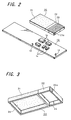
- FIG. 2 is a further exploded, perspective view of a circuit board and a shield case shown in FIG. 1;
- FIG. 3 is a perspective view seen from a different direction from the direction of FIG. 2;
- FIG. 4 is an exploded, perspective view of a and conventional communication terminal equipment.
- FIGS. 1 to 3 One mode for carrying out the present invention will be described hereinafter with reference to FIGS. 1 to 3 .
- FIG. 1 is an exploded perspective view of the portable telephone.
- a surface-side case 1 and a back surface-side case 2 formed of resin are joined to each other, thereby providing a terminal equipment constituted as a housing of the portable telephone.
- a plurality of operation keys 3 are arranged on the surface-side case 1 .
- a microphone 1 a , a speaker 1 b , a display panel member 4 and the like are arranged on the case 1 .
- the tip end portion of a rod-like whip antenna 5 is arranged at a position which becomes an upper side when using the equipment.
- the whip antenna 5 is attached to the back surface-side case 2 and constituted as an expandable antenna.
- the constitutions of the surface-side case 1 and the back surface-side case 2 are exactly the same as those of the surface-side case 1 and the back surface-side case 2 shown in FIG. 4 as prior art.
- a whip antenna connection section 11 is provided on the end portion of the circuit board 10 .
- FIG. 2 is a perspective view showing a state in which the shield case 20 is detached from the circuit board 10
- FIG. 3 is a perspective view showing the shield case 20 from the back surface side.
- the shield case 20 is constituted by a resin-formed member such as ABS resin and has a shield section 21 occupying about 2 ⁇ 3 of the case 20 and non-shield section 22 provided on the remaining portion.
- This non-shield section 22 is formed on a portion which become an upper side relative to the shield section 21 while being attached to the circuit board when this equipment is used as a portable telephone.
- the inside of the boundary portion between the shield section 21 and the non-shield section 22 is provided with a wall section 24 as shown in FIG. 3 .
- the shield section 21 of the shield case 20 has a conductor film formed to be coated on the surface of the case 20 and also coated on an inner surface 25 partitioned by the wall section 24 .
- This conductor film is brought into contact with the ground potential section (ground section) of the circuit board 10 to thereby obtain a shield effect for shielding the predetermined circuit components (e.g., circuit components 14 shown in FIG. 2) on the circuit board 10 covered with the shield case 20 .
- a shield case connection section 13 continuous to the ground potential section on the circuit is provided on the circuit board 10 .
- This connection section 13 is constituted to contact with the side surface of the shield section 21 of the shield case 20 when arranging the shield case 20 on the circuit board 10 .
- connection section 13 is made of, for example, an elastic metal member so as to ensure the contact of the connection section 13 with the shield case 20 by the elastic force of the section and to maintain a shield function.
- the inner surface 25 of the shield section 21 is also continuous to the ground potential section on the circuit.
- the shielding conductor film on the surface and the back surface of the shield section 21 is formed by, for example, coating tin by metal plating.
- An antenna pattern 23 is formed on the upper surface of the surface of the non-shield section 22 of the shield case 20 .
- This antenna pattern 23 is coated with, for example, copper by metal plating.
- the antenna pattern 23 is formed as a pattern wound helically with a predetermined size so as to function as a helical antenna as shown FIGS. 1 and 2.
- An end portion 23 a which is the outermost periphery of the wound pattern is arranged on the side wall (or in this case, an end portion which becomes an upper side when the equipment is used as a portable telephone) of the shield case 20 .
- the end portion 23 a of the antenna pattern 23 is constituted to contact with a feeder section 12 provided on the circuit board 10 .
- the feeder section 13 which serves as an antenna input terminal section of the circuit incorporated into the board, is constituted to contact with the end portion 23 a of the antenna pattern 23 of the shield case 20 .
- the feeder section 12 is formed of, for example, an elastic metal member to ensure the contact of the feeder section with the pattern 23 by the elastic force thereof, thereby maintaining the certainty of antenna connection.
- the communication terminal equipment in this example is constituted such that the helical antenna constituted by the antenna pattern 23 is used as an antenna for reception purpose only and the whip antenna 5 provided separately from the helical antenna as shown in FIG. 1 is used as an antenna for both transmission and reception purposes, and that diversity reception is conducted using one antenna capable of ensuring good signal reception out of the two antennas during reception.
- the helical antenna is formed integrally with the shield case 20 . Therefore, compared with a case where a helical antenna is attached to a circuit board as a separate member, the number of components of the communication terminal equipment can be reduced and the constitution of the communication terminal equipment can be thereby simplified. Further, as for the helical antenna attachment operativity, only by arranging the shield case 20 on the circuit board, the antenna can be simultaneously attached to the board. Thus, compared with a conventional case where the feeder section of an antenna is connected to a circuit board by soldering or the like, attachment can be made with quite simple operation.
- an elastic member is used as the feeder section 12 connected to the antenna pattern 23 constituting the helical antenna and the contact of the feeder section 12 with the antenna pattern 23 is ensured by the elastic force thereof.
- the antenna can be surely connected without the need to carry out any special connection operation.
- the present invention is applied to the helical antenna incorporated into the communication terminal equipment as a portable telephone.
- the present invention is also applicable to a helical antenna provided at other communication terminal equipment.
- the helical antenna is used as an antenna for reception purpose only.
- the helical antenna may be used as a transmission antenna or an antenna for both transmission and reception purposes.
- the shape of the antenna pattern constituting the helical antenna is not limited to the shape shown in FIGS. 1 and 2. Various patterns can be adopted as long as they have good reception characteristics or transmission characteristics as an antenna.
- the antenna pattern is arranged on the outer surface of a member constituting the shield case.
- the antenna pattern may be formed on the inner surface of the case.
- antenna patterns may be formed on both the outer surface and the inner surface of the member.
- the conductor pattern formed on the surface or the inner surface of the housing functions as an antenna element.
- the antenna can be attached to the circuit board, thereby constituting an antenna which can be easily attached to the equipment.
- the housing is the outer resin member having a conductor film arranged on a portion other than the neighborhood of a portion on which the conductor pattern is arranged, and the conductor film is brought into contact with the ground potential section of the circuit board to function as a shield, thereby constituting the antenna equipment integral with a shield case required by a communication equipment.
- the conductive pattern formed on the outer surface or the inner surface of the shield case functions as an antenna element.
- an antenna can be attached to the circuit board, whereby the number of components for the terminal equipment can be reduced accordingly, an antenna attachment step is not required and the assembly operativity of the terminal equipment enhances.
- the feeder section is constituted by a conductive member connected to the circuit board and having a predetermined elastic force, and the feeder section is made continuous to the conductor pattern by the elastic force of this member, whereby a soldering step is not required for the connection between the antenna and the circuit board and easy, good antenna connection can be ensured.
Landscapes
- Physics & Mathematics (AREA)
- Electromagnetism (AREA)
- Engineering & Computer Science (AREA)
- Computer Networks & Wireless Communication (AREA)
- Support Of Aerials (AREA)
- Details Of Aerials (AREA)
- Transceivers (AREA)
- Mobile Radio Communication Systems (AREA)
Applications Claiming Priority (2)
| Application Number | Priority Date | Filing Date | Title |
|---|---|---|---|
| JP29138299A JP2001111321A (ja) | 1999-10-13 | 1999-10-13 | アンテナ装置及び通信端末装置 |
| JP11-291382 | 1999-10-13 |
Publications (1)
| Publication Number | Publication Date |
|---|---|
| US6636725B1 true US6636725B1 (en) | 2003-10-21 |
Family
ID=17768207
Family Applications (1)
| Application Number | Title | Priority Date | Filing Date |
|---|---|---|---|
| US09/689,431 Expired - Fee Related US6636725B1 (en) | 1999-10-13 | 2000-10-12 | Antenna equipment and communication terminal equipment |
Country Status (5)
| Country | Link |
|---|---|
| US (1) | US6636725B1 (de) |
| EP (1) | EP1093183A3 (de) |
| JP (1) | JP2001111321A (de) |
| KR (1) | KR20010039987A (de) |
| CN (1) | CN1293462A (de) |
Cited By (9)
| Publication number | Priority date | Publication date | Assignee | Title |
|---|---|---|---|---|
| US20060160585A1 (en) * | 2004-11-18 | 2006-07-20 | Casio Hitachi Mobile Communications Co., Ltd. | Mobile wireless device |
| US20080285222A1 (en) * | 2007-05-18 | 2008-11-20 | Jae-Young Yeo | Chassis base assembly and display device including the same |
| US20090273537A1 (en) * | 2008-05-01 | 2009-11-05 | Chia-Lun Tang | Fm chip antenna |
| US20100255893A1 (en) * | 2009-04-07 | 2010-10-07 | Kabushiki Kaisha Toshiba | Mobile communication apparatus and antenna structure |
| US20100277377A1 (en) * | 2008-01-15 | 2010-11-04 | Panasonic Corporation | Portable wireless device |
| US20140378190A1 (en) * | 2013-06-21 | 2014-12-25 | Chiun Mai Communication Systems, Inc. | Wireless communication device |
| US20150002344A1 (en) * | 2013-07-01 | 2015-01-01 | Hyundai Motor Company | Antenna device for vehicle |
| US20160358064A1 (en) * | 2007-07-18 | 2016-12-08 | Murata Manufacturing Co., Ltd. | Radio ic device |
| EP3425728A1 (de) * | 2017-07-07 | 2019-01-09 | ProAnt AB | Verbinderbaugruppe |
Families Citing this family (17)
| Publication number | Priority date | Publication date | Assignee | Title |
|---|---|---|---|---|
| KR20030010261A (ko) * | 2001-07-26 | 2003-02-05 | 에스케이 텔레콤주식회사 | 루프 안테나를 갖는 휴대폰 |
| FR2833128A1 (fr) * | 2001-11-30 | 2003-06-06 | Sagem | Telephone mobile avec haut-parleur integre dans le volume de l'antenne |
| DE60204204T2 (de) * | 2001-11-30 | 2006-02-02 | Sagem S.A. | Mobiltelefon mit einem integrierten Element in dem Freiraum zwischen Antenne und der Schaltplatine |
| ATE551780T1 (de) | 2003-07-23 | 2012-04-15 | Lg Electronics Inc | Interne antenne und ein mobilendgerät mit dieser internen antenne |
| KR100652620B1 (ko) * | 2003-07-30 | 2006-12-06 | 엘지전자 주식회사 | 내장형 안테나가 구비된 휴대용 단말기 |
| KR200408694Y1 (ko) | 2005-10-04 | 2006-02-13 | 주식회사 이엠따블유안테나 | 초소형 내장형 안테나 |
| US7557763B2 (en) | 2005-10-18 | 2009-07-07 | Continental Automotive Systems Us, Inc. | Housing mounted Z-axis antenna coil |
| IL173941A0 (en) * | 2006-02-26 | 2007-03-08 | Haim Goldberger | Monolithic modules for high frequecney applications |
| JP5456231B2 (ja) * | 2006-10-30 | 2014-03-26 | 京セラ株式会社 | 携帯無線機 |
| JP5335187B2 (ja) * | 2006-10-30 | 2013-11-06 | 京セラ株式会社 | 携帯無線機 |
| CN101079519B (zh) * | 2007-05-31 | 2011-05-04 | 西安理工大学 | 能够接收超短波信号与卫星信号的组合天线 |
| JP5072443B2 (ja) * | 2007-06-07 | 2012-11-14 | 株式会社東芝 | 電子機器及びその製造方法 |
| JP4756020B2 (ja) * | 2007-09-25 | 2011-08-24 | 株式会社東芝 | 筐体及びその製造方法、並びに電子機器 |
| ATE500656T1 (de) * | 2008-05-08 | 2011-03-15 | Research In Motion Ltd | Mobile drahtlose kommunikationsvorrichtung mit verminderten schwingungen infolge von metallschirmkopplung |
| CN102723592B (zh) * | 2012-05-31 | 2016-02-10 | 深圳光启创新技术有限公司 | 一种内置型cmmb天线及通信终端 |
| JP2014179543A (ja) * | 2013-03-15 | 2014-09-25 | Hosiden Corp | 非接触給電装置および非接触受電装置 |
| FR3055767B1 (fr) * | 2016-09-08 | 2018-09-21 | Sagemcom Broadband Sas | Capot monobloc pour dispositif electronique |
Citations (5)
| Publication number | Priority date | Publication date | Assignee | Title |
|---|---|---|---|---|
| EP0790665A1 (de) | 1996-02-16 | 1997-08-20 | Murata Manufacturing Co., Ltd. | Chipantenne |
| EP0848448A2 (de) | 1996-12-10 | 1998-06-17 | Murata Manufacturing Co., Ltd. | Oberflächenmontierte Antenne und Kommunikationsgerät mit einer derartigen Antenne |
| WO1999043041A1 (en) | 1998-02-20 | 1999-08-26 | Qualcomm Incorporated | Substrate antenna incorporating an element preventing the coupling of energy between antenna and conductors |
| US5969682A (en) * | 1995-04-10 | 1999-10-19 | Sony Corporation | Antenna apparatus and portable radio apparatus |
| US6434369B1 (en) * | 1998-08-12 | 2002-08-13 | Sony Corporation | Antenna device and portable transceiver |
-
1999
- 1999-10-13 JP JP29138299A patent/JP2001111321A/ja active Pending
-
2000
- 2000-10-04 KR KR1020000058134A patent/KR20010039987A/ko not_active Withdrawn
- 2000-10-11 EP EP00308939A patent/EP1093183A3/de not_active Withdrawn
- 2000-10-12 US US09/689,431 patent/US6636725B1/en not_active Expired - Fee Related
- 2000-10-13 CN CN00130480A patent/CN1293462A/zh active Pending
Patent Citations (5)
| Publication number | Priority date | Publication date | Assignee | Title |
|---|---|---|---|---|
| US5969682A (en) * | 1995-04-10 | 1999-10-19 | Sony Corporation | Antenna apparatus and portable radio apparatus |
| EP0790665A1 (de) | 1996-02-16 | 1997-08-20 | Murata Manufacturing Co., Ltd. | Chipantenne |
| EP0848448A2 (de) | 1996-12-10 | 1998-06-17 | Murata Manufacturing Co., Ltd. | Oberflächenmontierte Antenne und Kommunikationsgerät mit einer derartigen Antenne |
| WO1999043041A1 (en) | 1998-02-20 | 1999-08-26 | Qualcomm Incorporated | Substrate antenna incorporating an element preventing the coupling of energy between antenna and conductors |
| US6434369B1 (en) * | 1998-08-12 | 2002-08-13 | Sony Corporation | Antenna device and portable transceiver |
Cited By (13)
| Publication number | Priority date | Publication date | Assignee | Title |
|---|---|---|---|---|
| US20060160585A1 (en) * | 2004-11-18 | 2006-07-20 | Casio Hitachi Mobile Communications Co., Ltd. | Mobile wireless device |
| US20080285222A1 (en) * | 2007-05-18 | 2008-11-20 | Jae-Young Yeo | Chassis base assembly and display device including the same |
| US10373043B2 (en) * | 2007-07-18 | 2019-08-06 | Murata Manufacturing Co., Ltd. | Radio IC device |
| US20160358064A1 (en) * | 2007-07-18 | 2016-12-08 | Murata Manufacturing Co., Ltd. | Radio ic device |
| US8203493B2 (en) * | 2008-01-15 | 2012-06-19 | Panasonic Corporation | Portable wireless device |
| US20100277377A1 (en) * | 2008-01-15 | 2010-11-04 | Panasonic Corporation | Portable wireless device |
| US7733292B2 (en) * | 2008-05-01 | 2010-06-08 | Auden Techno Corp. | FM chip antenna |
| US20090273537A1 (en) * | 2008-05-01 | 2009-11-05 | Chia-Lun Tang | Fm chip antenna |
| US20100255893A1 (en) * | 2009-04-07 | 2010-10-07 | Kabushiki Kaisha Toshiba | Mobile communication apparatus and antenna structure |
| US20140378190A1 (en) * | 2013-06-21 | 2014-12-25 | Chiun Mai Communication Systems, Inc. | Wireless communication device |
| US9191471B2 (en) * | 2013-06-21 | 2015-11-17 | Chiun Mai Communication Systems, Inc. | Wireless communication device |
| US20150002344A1 (en) * | 2013-07-01 | 2015-01-01 | Hyundai Motor Company | Antenna device for vehicle |
| EP3425728A1 (de) * | 2017-07-07 | 2019-01-09 | ProAnt AB | Verbinderbaugruppe |
Also Published As
| Publication number | Publication date |
|---|---|
| KR20010039987A (ko) | 2001-05-15 |
| CN1293462A (zh) | 2001-05-02 |
| EP1093183A3 (de) | 2001-11-14 |
| EP1093183A2 (de) | 2001-04-18 |
| JP2001111321A (ja) | 2001-04-20 |
Similar Documents
| Publication | Publication Date | Title |
|---|---|---|
| EP1093183A2 (de) | Antennenausrüstung und Kommunikationsendgerät | |
| US6563042B2 (en) | Radiating enclosure | |
| US10673126B2 (en) | Antenna device for portable terminal | |
| US5177492A (en) | Rod antenna mounting mechanism of radio terminal equipment | |
| EP1501202B1 (de) | Interne Antenne und ein Mobilendgerät mit dieser internen Antenne | |
| TWI389387B (zh) | 具有減少射頻訊號干擾的無線可攜式裝置 | |
| EP0755091A1 (de) | Antenne für zwei frequenzbänder | |
| JP2006166370A (ja) | 折畳式携帯無線機 | |
| KR100816262B1 (ko) | 전자 기기 하우징 내장형 안테나 및 그 제조방법 | |
| KR100649791B1 (ko) | 안테나와 컨덕터들 사이의 에너지 커플링을 방지하는 요소를 편입한 기판 안테나 | |
| US6434369B1 (en) | Antenna device and portable transceiver | |
| US6700545B2 (en) | Antenna apparatus and transmission/reception apparatus having such an antenna apparatus | |
| US7656354B2 (en) | Antenna apparatus for portable terminal | |
| JP2003101326A (ja) | 平板多重アンテナおよびそれを備えた電気機器 | |
| KR100738265B1 (ko) | 기판 안테나 | |
| KR20210047814A (ko) | 소형 기기용 안테나 모듈 | |
| JP2001036319A (ja) | 携帯端末 | |
| US7439910B2 (en) | Three-dimensional antenna structure | |
| JP2006093998A (ja) | 携帯通信機 | |
| JP2003143274A (ja) | 携帯無線端末装置 | |
| JP2005159908A (ja) | アンテナ | |
| JP3050494B2 (ja) | 無線機用アンテナ | |
| KR20040000535A (ko) | 이동 통신 단말기의 내장형 gps안테나 | |
| KR200253156Y1 (ko) | 이동통신 단말기의 안테나 | |
| KR101390098B1 (ko) | 이동단말기 |
Legal Events
| Date | Code | Title | Description |
|---|---|---|---|
| AS | Assignment |
Owner name: SONY CORPORATION, JAPAN Free format text: ASSIGNMENT OF ASSIGNORS INTEREST;ASSIGNOR:YOSHIMOTO, HIROMASA;REEL/FRAME:011475/0260 Effective date: 20010112 |
|
| REMI | Maintenance fee reminder mailed | ||
| LAPS | Lapse for failure to pay maintenance fees | ||
| STCH | Information on status: patent discontinuation |
Free format text: PATENT EXPIRED DUE TO NONPAYMENT OF MAINTENANCE FEES UNDER 37 CFR 1.362 |
|
| FP | Lapsed due to failure to pay maintenance fee |
Effective date: 20071021 |