US6628362B2 - In-plane switching mode liquid crystal display device having a high aperture ratio - Google Patents
In-plane switching mode liquid crystal display device having a high aperture ratio Download PDFInfo
- Publication number
- US6628362B2 US6628362B2 US09/781,189 US78118901A US6628362B2 US 6628362 B2 US6628362 B2 US 6628362B2 US 78118901 A US78118901 A US 78118901A US 6628362 B2 US6628362 B2 US 6628362B2
- Authority
- US
- United States
- Prior art keywords
- liquid crystal
- display device
- crystal display
- switching mode
- substrate
- Prior art date
- Legal status (The legal status is an assumption and is not a legal conclusion. Google has not performed a legal analysis and makes no representation as to the accuracy of the status listed.)
- Expired - Lifetime
Links
Images

Classifications
-
- G—PHYSICS
- G02—OPTICS
- G02F—OPTICAL DEVICES OR ARRANGEMENTS FOR THE CONTROL OF LIGHT BY MODIFICATION OF THE OPTICAL PROPERTIES OF THE MEDIA OF THE ELEMENTS INVOLVED THEREIN; NON-LINEAR OPTICS; FREQUENCY-CHANGING OF LIGHT; OPTICAL LOGIC ELEMENTS; OPTICAL ANALOGUE/DIGITAL CONVERTERS
- G02F1/00—Devices or arrangements for the control of the intensity, colour, phase, polarisation or direction of light arriving from an independent light source, e.g. switching, gating or modulating; Non-linear optics
- G02F1/01—Devices or arrangements for the control of the intensity, colour, phase, polarisation or direction of light arriving from an independent light source, e.g. switching, gating or modulating; Non-linear optics for the control of the intensity, phase, polarisation or colour
- G02F1/13—Devices or arrangements for the control of the intensity, colour, phase, polarisation or direction of light arriving from an independent light source, e.g. switching, gating or modulating; Non-linear optics for the control of the intensity, phase, polarisation or colour based on liquid crystals, e.g. single liquid crystal display cells
- G02F1/133—Constructional arrangements; Operation of liquid crystal cells; Circuit arrangements
- G02F1/1333—Constructional arrangements; Manufacturing methods
- G02F1/1343—Electrodes
-
- G—PHYSICS
- G02—OPTICS
- G02F—OPTICAL DEVICES OR ARRANGEMENTS FOR THE CONTROL OF LIGHT BY MODIFICATION OF THE OPTICAL PROPERTIES OF THE MEDIA OF THE ELEMENTS INVOLVED THEREIN; NON-LINEAR OPTICS; FREQUENCY-CHANGING OF LIGHT; OPTICAL LOGIC ELEMENTS; OPTICAL ANALOGUE/DIGITAL CONVERTERS
- G02F1/00—Devices or arrangements for the control of the intensity, colour, phase, polarisation or direction of light arriving from an independent light source, e.g. switching, gating or modulating; Non-linear optics
- G02F1/01—Devices or arrangements for the control of the intensity, colour, phase, polarisation or direction of light arriving from an independent light source, e.g. switching, gating or modulating; Non-linear optics for the control of the intensity, phase, polarisation or colour
- G02F1/13—Devices or arrangements for the control of the intensity, colour, phase, polarisation or direction of light arriving from an independent light source, e.g. switching, gating or modulating; Non-linear optics for the control of the intensity, phase, polarisation or colour based on liquid crystals, e.g. single liquid crystal display cells
- G02F1/133—Constructional arrangements; Operation of liquid crystal cells; Circuit arrangements
- G02F1/136—Liquid crystal cells structurally associated with a semi-conducting layer or substrate, e.g. cells forming part of an integrated circuit
- G02F1/1362—Active matrix addressed cells
- G02F1/136213—Storage capacitors associated with the pixel electrode
-
- G—PHYSICS
- G02—OPTICS
- G02F—OPTICAL DEVICES OR ARRANGEMENTS FOR THE CONTROL OF LIGHT BY MODIFICATION OF THE OPTICAL PROPERTIES OF THE MEDIA OF THE ELEMENTS INVOLVED THEREIN; NON-LINEAR OPTICS; FREQUENCY-CHANGING OF LIGHT; OPTICAL LOGIC ELEMENTS; OPTICAL ANALOGUE/DIGITAL CONVERTERS
- G02F1/00—Devices or arrangements for the control of the intensity, colour, phase, polarisation or direction of light arriving from an independent light source, e.g. switching, gating or modulating; Non-linear optics
- G02F1/01—Devices or arrangements for the control of the intensity, colour, phase, polarisation or direction of light arriving from an independent light source, e.g. switching, gating or modulating; Non-linear optics for the control of the intensity, phase, polarisation or colour
- G02F1/13—Devices or arrangements for the control of the intensity, colour, phase, polarisation or direction of light arriving from an independent light source, e.g. switching, gating or modulating; Non-linear optics for the control of the intensity, phase, polarisation or colour based on liquid crystals, e.g. single liquid crystal display cells
- G02F1/133—Constructional arrangements; Operation of liquid crystal cells; Circuit arrangements
- G02F1/1333—Constructional arrangements; Manufacturing methods
- G02F1/1343—Electrodes
- G02F1/134309—Electrodes characterised by their geometrical arrangement
- G02F1/134363—Electrodes characterised by their geometrical arrangement for applying an electric field parallel to the substrate, i.e. in-plane switching [IPS]
Definitions
- the present invention relates to a liquid crystal display device, and more particularly, an in-plane switching mode liquid crystal display device having a high aperture ratio.
- Twisted nematic liquid crystal display devices (hereinafter TN LCDs) having high image quality and low power consumption are widely applied to flat panel display devices.
- the TN LCDs however, have a narrow viewing angle due to refractive anisotropy of liquid crystal molecules.
- a multi-domain LCD such as a two-domain TN LCD(TDTN LCD) and a domain divided TN LCD(DDTN LCD), and a TN LCD including an optical compensation film have been introduced.
- a contrast ratio is decreased and a color shift is generated depending on a viewing angle.
- an in-plane switching mode LCD is also proposed.
- the in-plane switching mode liquid crystal display device which is suggested to materialize wide viewing angle, is disclosed in the JAPAN DISPLAY 92 P547, Japanese Patent Unexamined Publication No. 7-36058, Japanese Patent Unexamined Publication No. 7-225388 and ASIA DISPLAY 95 P707, and etc.
- FIG. 1A is a plan view of a unit pixel of a conventional in-plane switching mode active matrix LCD.
- FIG. 1B is a sectional view according to line I-I′ of FIG. 1 A.
- the apparatus comprises a gate bus line 1 and a data bus line 2 in which the lines 1 , 2 are perpendicularly arranged in a matrix form on a transparent first substrate 10 thereby defining an unit pixel region, a common line 3 arranged parallel to the gate bus line 1 in the pixel region, thin film transistor (TFT) formed adjacent a cross point of the gate bus line 1 and the data bus line 2 , and a data electrode 8 and a common electrode 9 formed in the pixel region.
- TFT thin film transistor
- the TFT includes a gate electrode 5 electrically coupled with the gate bus line 1 , a gate insulator 12 on the gate electrode 5 , a semiconductor layer 15 on the gate insulator 12 , a channel layer on the semiconductor layer 15 , and source/drain electrodes 6 , 7 which are electrically coupled the data bus line 2 and the data electrode 8 respectively.
- the common electrode 9 is formed concurrently with the gate electrode 5 and electrically coupled to the common line 3 . Further, a passivation layer 20 and a first alignment layer 23 a are deposited on the inner surface of the first substrate 10 .
- a black matrix 28 is formed to prevent a light leakage generating around the TFT, the gate bus line 1 , and the data bus line 2 .
- a color filter layer 29 , an over-coat layer (not illustrated), and a second alignment layer 23 b are formed on the black matrix 28 in sequence.
- a liquid crystal layer 30 is formed between the first and second alignment layers 23 a, 23 b.
- a storage capacitor in a liquid crystal display device is applied to prevent the apparatus from a gray inversion, a flicker, and an afterimage.
- Methods of forming this storage capacitor are divided into a storage on gate (SOG) mode and a storage on common (SOC) mode.
- SOG storage on gate
- SOC storage on common
- SOG SOG
- some part of the (n ⁇ 1) th gate bus line is applied as a storage capacitor in the n th pixel region.
- a separated electrode for storage capacitor is electrically coupled to the common electrode.
- the aperture ratio is decreased, and the metal lines may cause a short state, thereby decreasing a yield.
- the present invention is directed to an in-plane switching mode LCD that substantially obviates one or more of the problems due to limitations and disadvantages of the related art.
- An object of the present invention is to provide an in-plane switching mode LCD having the high aperture ratio and the high yield by using the SOG mode storage capacitor only, or both SOG mode storage capacitor and SOC mode storage capacitor.
- an in-plane switching mode liquid crystal display device comprises first and second substrates; a data bus line and a gate bus line arranged in a matrix on said first substrate and defining a unit pixel region; a thin film transistor (TFT) formed adjacent a cross point of the gate bus line and the data bus line, and a data electrode which partially covers adjacent the gate bus line; a passivation layer on the TFT and the data electrode; a common electrode substantially parallel to the data electrode and covering the gate bus lines of n th and (n+1) th , or n th and (n ⁇ 1) th ; a common line covering the gate bus lines of n th and (n+1) th , or n th and (n ⁇ 1) th ; a first alignment layer on the common electrode; a black matrix for preventing a light leakage which is generated around the TFT, the gate bus line, and the data bus line;
- a storage capacitor is formed by the gate bus line, the data electrode, and the common electrode or the common line.
- certain part of the data electrode covers the n th gate bus line.
- a part of the common electrode covers adjacent the data electrode and another part of the common electrode does not cover the opposite data electrode and the gate bus line.
- the storage capacitor is formed by the gate bus line, the data electrode, and the common electrode or the common line.
- a liquid crystal display device has a substrate, first and second gate lines arranged substantially in parallel above the substrate, a bus line arranged to intersect the first and second gate lines to define a pixel, a transistor having a source and a drain formed near an intersection part of the bus line and the first gate line, the source being connected to the bus line, and at least one data electrode connected to the drain of the transistor.
- a passivation layer is generally formed above the transistors and the at least one data electrode.
- at least one common electrode is arranged above the passivation layer in parallel with the second gate line, the common electrode and the data electrode. In this configuration, the portions of at least two of the second gate line, the data electrode and the common electrode are overlapping with each other.
- the portions of the second gate line, the data electrode and the common electrode all overlap with each other.
- the second gate line has no overlapping portions with the data electrode and the common electrode.
- the data electrode has no overlapping portions with the common electrode.
- the second gate line has no overlapping portions with the common electrode.
- FIG. 1A is a plan view of a unit pixel of a conventional in-plane switching mode LCD
- FIG. 1B is a sectional view according to line I-I′ of FIG. 1A;
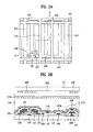
- FIG. 2A is a plan view of a unit pixel according to a first embodiment of the present invention.
- FIG. 2B is a sectional view according to line II-II′ of FIG. 2A;
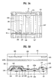
- FIG. 3A is a plan view of a unit pixel according to a second embodiment of the present invention.
- FIG. 3B is a sectional view according to line III-III′ of FIG. 3A;
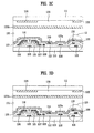
- FIG. 3C is a sectional view of a third embodiment of the present invention.
- FIG. 3D is a sectional view of a fourth embodiment of the present invention.
- FIG. 2A is a plan view of a unit pixel according to a first embodiment of the present invention.
- FIG. 2B is a sectional view according to line II-II′ of FIG. 2 A.
- two gate bus lines 101 , 101 ′ and two data bus line 102 , 102 ′ are perpendicularly arranged in a matrix form on a transparent first substrate 110 thereby defining the unit pixel region.
- LCDs have a plurality of pixel regions(n ⁇ m) including a large number of gate bus line(n) and data bus line(m).
- a gate insulator 112 is formed on the gate bus lines 101 , 101 ′.
- the gate insulator 112 made of any suitable non-conductive materials, such as SiNx and SiOx, is formed on the gate electrode preferably by chemical vapor deposition(CVD) method.
- a semiconductor layer 115 as channel layer is formed on the gate insulator 112 by depositing and etching an a-Si.
- An ohmic contact layer 116 made of a n + a-Si is formed on the semiconductor layer 115 .
- the data bus lines 102 , 102 ′, a source electrode 106 , and a data electrode 108 are formed above the ohmic contact layer 116 and the gate insulator 112 .
- the data electrode 108 is formed by etching a metal thin film preferably made of Al, Cr, Ti, or Al alloy after they are deposited on the gate insulator 112 by a sputtering method.
- the gate electrode made of Cr is patterned. After that, on the substrate which the gate bus line is patterned, the gate insulator, the semiconductor layer and the ohmic contact layer are formed in sequence. The data electrode and the source/drain electrode are formed by depositing and patterning Cr after pad opening.
- the passivation layer 120 is formed on the TFT, the data bus lines 102 , 102 ′, the data electrode 108 , and the gate insulator 112 by depositing an inorganic material, such as SiNx or SiOx, or an organic material such as benzocyclobutene(BCB).
- an inorganic material such as SiNx or SiOx
- an organic material such as benzocyclobutene(BCB).
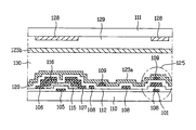
- a common electrode 109 and common bus line 103 are formed by etching a thin metal film preferably made of Al, Mo, Ta, Cr, Al, or indium tin oxide(ITO) alloy after they are deposited on the substrate 110 by a sputtering method, then a first alignment layer 123 a is formed thereon.
- the common electrode 109 which is substantially parallel to the data electrode 108 is formed on the gate bus lines 101 , 101 ′.
- a circular mark 125 represents a group of electrodes which are overlapped to form a storage capacitor.
- the storage capacitor is formed by the common electrode 109 which is substantially parallel to the data electrode 108 and covers the gate bus lines of n th and (n+1) th , or n th and (n ⁇ 1) th and the common line which is on a same plane of the common electrode and covers the gate bus lines of n th and (n+1) th , or n th and (n ⁇ 1) th .
- a black matrix 128 is formed to, prevent a light leakage generating around the TFT, the gate bus lines 101 , 101 ′ and the data bus lines 102 , 102 ′ by etching a thin layer made of Cr, CrOx, or black resin which are deposited by sputtering method.
- a color filter layer 129 , an over-coat layer (not shown), and a second alignment layer 123 b are formed on the black matrix 128 in sequence, as shown in FIG. 2 B.
- a liquid crystal layer 130 is formed between the first and second alignment layers 123 a , 123 b.
- each of alignment directions of the first and second alignment layers 123 a , 123 b is determined by a rubbing method using polyamide, polyimide, SiO 2 , polyvinylalcohol(PVA) or polyamic acid, or by photo-alignment method using photosensitive material such as polyvinylcinnamate(PVCN), polysiloxanecinnamate(PSCN) or cellulosecinnamate(CelCN).
- PVCN polyvinylcinnamate
- PSCN polysiloxanecinnamate
- CelCN cellulosecinnamate
- FIG. 3A is a plan view of a unit pixel according to a second embodiment of the present invention.
- FIG. 3B is a sectional view according to line III-III′ of FIG. 3 A.
- the common electrode 119 and the common line 103 cover some part of the data electrode 108 but do not cover the gate bus lines 101 , 101 ′.
- FIG. 3C is a sectional view of a third embodiment of the present invention.
- the common electrode 119 overlaps the data electrode 108 .
- the common electrode 119 and the data electrode 108 do not overlap any portion of the gate bus line 101 .
- the overlapping of the common electrode 119 and the data electrode 108 in effect creates a capacitor between the two layers.
- FIG. 3D is a sectional view of a fourth embodiment of the present invention.
- the common electrode 119 does not overlap the data electrode 108 , but overlaps the gate bus line 101 .
- certain portions of the data electrode 108 overlaps the gate bus line 101 .
- the above conductive lines and electrodes in effect creates a capacitor between two overlapping conductive layers.
- certain capacitance is formed even between non-overlapping conductive layers which are in near vicinity of each other.
Landscapes
- Physics & Mathematics (AREA)
- Nonlinear Science (AREA)
- Mathematical Physics (AREA)
- Chemical & Material Sciences (AREA)
- Crystallography & Structural Chemistry (AREA)
- General Physics & Mathematics (AREA)
- Optics & Photonics (AREA)
- Engineering & Computer Science (AREA)
- Geometry (AREA)
- Power Engineering (AREA)
- Microelectronics & Electronic Packaging (AREA)
- Liquid Crystal (AREA)
Abstract
Description
Claims (14)
Priority Applications (1)
| Application Number | Priority Date | Filing Date | Title |
|---|---|---|---|
| US09/781,189 US6628362B2 (en) | 1998-01-23 | 2001-02-13 | In-plane switching mode liquid crystal display device having a high aperture ratio |
Applications Claiming Priority (5)
| Application Number | Priority Date | Filing Date | Title |
|---|---|---|---|
| KR98-02121 | 1998-01-23 | ||
| KR1019980002121A KR100293436B1 (en) | 1998-01-23 | 1998-01-23 | In plane switching mode liquid crystal display device |
| KR1998-02121 | 1998-01-23 | ||
| US09/235,205 US6445435B1 (en) | 1998-01-23 | 1999-01-21 | In-plane switching mode liquid cystal display device having common electrode on passivation layer |
| US09/781,189 US6628362B2 (en) | 1998-01-23 | 2001-02-13 | In-plane switching mode liquid crystal display device having a high aperture ratio |
Related Parent Applications (1)
| Application Number | Title | Priority Date | Filing Date |
|---|---|---|---|
| US09/235,205 Division US6445435B1 (en) | 1997-07-29 | 1999-01-21 | In-plane switching mode liquid cystal display device having common electrode on passivation layer |
Publications (2)
| Publication Number | Publication Date |
|---|---|
| US20020008825A1 US20020008825A1 (en) | 2002-01-24 |
| US6628362B2 true US6628362B2 (en) | 2003-09-30 |
Family
ID=19532036
Family Applications (2)
| Application Number | Title | Priority Date | Filing Date |
|---|---|---|---|
| US09/235,205 Expired - Lifetime US6445435B1 (en) | 1997-07-29 | 1999-01-21 | In-plane switching mode liquid cystal display device having common electrode on passivation layer |
| US09/781,189 Expired - Lifetime US6628362B2 (en) | 1998-01-23 | 2001-02-13 | In-plane switching mode liquid crystal display device having a high aperture ratio |
Family Applications Before (1)
| Application Number | Title | Priority Date | Filing Date |
|---|---|---|---|
| US09/235,205 Expired - Lifetime US6445435B1 (en) | 1997-07-29 | 1999-01-21 | In-plane switching mode liquid cystal display device having common electrode on passivation layer |
Country Status (2)
| Country | Link |
|---|---|
| US (2) | US6445435B1 (en) |
| KR (1) | KR100293436B1 (en) |
Cited By (6)
| Publication number | Priority date | Publication date | Assignee | Title |
|---|---|---|---|---|
| US20030095229A1 (en) * | 2001-10-02 | 2003-05-22 | Hiroyasu Inoue | Liquid crystal display device and method of fabricating the same |
| US20050151913A1 (en) * | 2004-01-13 | 2005-07-14 | Innolux Display Corp. | In-plane switching liquid crystal display device having storage capacitors |
| US20080316406A1 (en) * | 2001-10-02 | 2008-12-25 | Sharp Kabushiki Kaisha | Liquid crystal display device and method of fabricating the same |
| US20100196998A1 (en) * | 2004-06-08 | 2010-08-05 | Life Technologies Corporation | System and method for electroporating a sample |
| US20140061818A1 (en) * | 2012-03-16 | 2014-03-06 | Boe Technology Group Co., Ltd. | Tft array subsrate, fabrication method, and display device thereof |
| US20220317109A1 (en) * | 2020-12-04 | 2022-10-06 | The United States Department of Transportation / Federal Highway Administration | Method for the assessment of alkali-silica reactivity of aggregates and concrete mixtures |
Families Citing this family (21)
| Publication number | Priority date | Publication date | Assignee | Title |
|---|---|---|---|---|
| KR100225910B1 (en) | 1996-04-04 | 1999-10-15 | 구자홍 | LIQUID CRYSTAL DISPLAY DEVICE |
| US6532053B2 (en) | 1996-12-18 | 2003-03-11 | Hitachi, Ltd. | Transverse electric field system liquid crystal display device suitable for improving aperture ratio |
| US6441401B1 (en) * | 1999-03-19 | 2002-08-27 | Samsung Electronics Co., Ltd. | Thin film transistor array panel for liquid crystal display and method for repairing the same |
| JP4724339B2 (en) * | 1999-09-07 | 2011-07-13 | 株式会社日立製作所 | Liquid crystal display |
| JP2001201766A (en) * | 2000-01-18 | 2001-07-27 | Hitachi Ltd | Manufacturing method of liquid crystal display device |
| JP3542023B2 (en) * | 2000-03-16 | 2004-07-14 | インターナショナル・ビジネス・マシーンズ・コーポレーション | Liquid crystal display |
| KR20020017047A (en) * | 2000-08-28 | 2002-03-07 | 구본준, 론 위라하디락사 | liquid crystal display device and manufacturing method thereof |
| KR100587367B1 (en) * | 2000-10-20 | 2006-06-08 | 엘지.필립스 엘시디 주식회사 | Transverse electric field liquid crystal display device and manufacturing method thereof |
| TW575775B (en) * | 2001-01-29 | 2004-02-11 | Hitachi Ltd | Liquid crystal display device |
| JP2002258320A (en) * | 2001-02-28 | 2002-09-11 | Nec Corp | Liquid crystal display device |
| KR100807582B1 (en) * | 2001-07-30 | 2008-02-28 | 엘지.필립스 엘시디 주식회사 | Storage Capacitor and Liquid Crystal Display With Same |
| US20050120761A1 (en) * | 2003-12-03 | 2005-06-09 | Rouleau James E. | Column assembly of a vehicle having a steering column to be locked and unlocked |
| KR101109978B1 (en) * | 2004-12-13 | 2012-02-29 | 엘지디스플레이 주식회사 | High aperture ratio liquid crystal display device |
| TW200706955A (en) * | 2005-08-08 | 2007-02-16 | Innolux Display Corp | In-plane switching liquid crystal display device |
| JP2008164787A (en) | 2006-12-27 | 2008-07-17 | Epson Imaging Devices Corp | Liquid crystal display device |
| JP5246782B2 (en) | 2008-03-06 | 2013-07-24 | 株式会社ジャパンディスプレイウェスト | Liquid crystal device and electronic device |
| KR20100034874A (en) * | 2008-09-25 | 2010-04-02 | 삼성전자주식회사 | Display having a planarized substrate and method of the same |
| US20110085121A1 (en) * | 2009-10-08 | 2011-04-14 | Hydis Technologies Co., Ltd. | Fringe Field Switching Mode Liquid Crystal Display Device and Method of Fabricating the Same |
| CN103869558B (en) * | 2014-03-31 | 2017-02-15 | 昆山龙腾光电有限公司 | Liquid crystal display device and manufacturing method thereof |
| WO2015178028A1 (en) * | 2014-05-23 | 2015-11-26 | 株式会社Joled | Organic el display panel and organic el display device |
| CN104298018B (en) * | 2014-09-23 | 2018-05-04 | 京东方科技集团股份有限公司 | Array base palte and preparation method thereof, display panel |
Citations (64)
| Publication number | Priority date | Publication date | Assignee | Title |
|---|---|---|---|---|
| US4239346A (en) | 1979-05-23 | 1980-12-16 | Hughes Aircraft Company | Compact liquid crystal display system |
| EP0036820A1 (en) | 1980-03-26 | 1981-09-30 | COMMISSARIAT A L'ENERGIE ATOMIQUE Etablissement de Caractère Scientifique Technique et Industriel | Device for the limitation of the effects of axial hydraulic pressure on the fuel assemblies of a nuclear reactor |
| JPS60158421A (en) | 1984-01-28 | 1985-08-19 | Seiko Instr & Electronics Ltd | Matrix liquid crystal display device |
| JPS6278532A (en) | 1985-10-02 | 1987-04-10 | Hitachi Ltd | liquid crystal display element |
| US4726659A (en) | 1986-02-24 | 1988-02-23 | Rca Corporation | Display device having different alignment layers |
| JPH0467127A (en) | 1990-07-09 | 1992-03-03 | Hitachi Ltd | lcd display panel |
| EP0588568A2 (en) | 1992-09-18 | 1994-03-23 | Hitachi, Ltd. | A liquid crystal display device |
| US5307189A (en) | 1991-03-05 | 1994-04-26 | Oki Electric Industry Co., Ltd. | Active-matrix-addressed liquid crystal with conductor collecting lines of force emanating from data electrode |
| JPH06160878A (en) | 1992-09-18 | 1994-06-07 | Hitachi Ltd | Liquid crystal display |
| US5321535A (en) | 1990-07-23 | 1994-06-14 | Hosiden Corporation | Liquid crystal display device with control capacitors for gray scale |
| JPH06273803A (en) | 1993-01-20 | 1994-09-30 | Hitachi Ltd | Active matrix liquid crystal display device |
| JPH0736058A (en) | 1993-07-20 | 1995-02-07 | Hitachi Ltd | Active matrix liquid crystal display |
| JPH07134301A (en) | 1993-11-09 | 1995-05-23 | Hitachi Ltd | Liquid crystal display |
| JPH07225388A (en) | 1994-02-14 | 1995-08-22 | Hitachi Ltd | Active matrix liquid crystal display device |
| US5459596A (en) | 1992-09-14 | 1995-10-17 | Kabushiki Kaisha Toshiba | Active matrix liquid crystal display with supplemental capacitor line which overlaps signal line |
| US5464669A (en) | 1993-09-18 | 1995-11-07 | Goldstar Co., Ltd. | Method for forming an orientation film of photopolymer in a liquid crystal display |
| US5492762A (en) | 1990-11-21 | 1996-02-20 | Catalysts & Chemicals Industries Co., Ltd. | Conductive substrate and display device provided with transparent conductive substrate |
| JPH0862586A (en) | 1994-08-19 | 1996-03-08 | Matsushita Electric Ind Co Ltd | Liquid crystal display element |
| KR960032049A (en) | 1995-02-01 | 1996-09-17 | 가나이 쯔또무 | Liquid crystal panel and liquid crystal display device |
| US5576858A (en) | 1991-10-14 | 1996-11-19 | Hosiden Corporation | Gray scale LCD control capacitors formed between a control capacitor electrode on one side of an insulating layer and two subpixel electrodes on the other side |
| EP0749029A1 (en) | 1995-06-14 | 1996-12-18 | Hitachi, Ltd. | Liquid crystal display device with wide viewing angle characteristics comprising a high resistivity black matrix |
| JPH095763A (en) | 1995-06-14 | 1997-01-10 | Hitachi Ltd | Color liquid crystal display |
| JPH095764A (en) | 1995-06-20 | 1997-01-10 | Hitachi Ltd | LCD display substrate |
| JPH095793A (en) | 1996-07-31 | 1997-01-10 | Hitachi Ltd | Liquid crystal display |
| US5600464A (en) | 1993-09-20 | 1997-02-04 | Hitachi, Ltd. | Liquid crystal display device having the electric field parallel to the substrates |
| JPH0933946A (en) | 1995-07-17 | 1997-02-07 | Hitachi Ltd | Active matrix type liquid crystal display device and manufacturing method thereof |
| US5602662A (en) | 1993-06-21 | 1997-02-11 | Case Western Reserve University | Cholesteric liquid crystal devices |
| JPH0943589A (en) | 1995-07-27 | 1997-02-14 | Hitachi Ltd | Liquid crystal display |
| JPH0943590A (en) | 1995-07-27 | 1997-02-14 | Hitachi Ltd | Liquid crystal display |
| US5608556A (en) | 1993-06-24 | 1997-03-04 | Sanyo Electric Co., Ltd. | Liquid crystal display having orientation control electrodes for controlling liquid crystal orientation |
| WO1997010530A1 (en) | 1995-09-14 | 1997-03-20 | Hitachi, Ltd. | Active matrix liquid crystal display |
| JPH09101538A (en) | 1995-10-04 | 1997-04-15 | Hitachi Ltd | Active matrix type liquid crystal display device and manufacturing method thereof |
| JPH09105908A (en) | 1995-10-09 | 1997-04-22 | Hitachi Ltd | Active matrix type liquid crystal display |
| JPH09105918A (en) | 1995-10-12 | 1997-04-22 | Hitachi Ltd | Liquid crystal display |
| KR970022458A (en) | 1995-10-04 | 1997-05-28 | 카나이 쯔또무 | Transverse electric field type liquid crystal display device composed of liquid crystal molecules having two or more kinds of reorientation directions and a manufacturing method thereof |
| US5646705A (en) | 1991-09-26 | 1997-07-08 | Kabushiki Kaisha Toshiba | Electrode structure of liquid crystal display device and method of manufacturing the liquid crystal display device |
| JPH09258269A (en) | 1996-03-27 | 1997-10-03 | Hitachi Ltd | Liquid crystal display |
| JPH09269507A (en) | 1996-03-29 | 1997-10-14 | Hosiden Corp | Liquid crystal display element |
| US5686019A (en) | 1994-05-17 | 1997-11-11 | Canon Kabushiki Kaisha | Liquid crystal device and liquid crystal apparatus |
| JPH09325346A (en) | 1996-06-03 | 1997-12-16 | Sharp Corp | Liquid crystal display device and driving method thereof |
| US5742369A (en) | 1993-12-28 | 1998-04-21 | Canon Kabushiki Kaisha | Method of aligning liquid crystals by applying an alternating electric field under periodically changing temperature |
| US5745207A (en) | 1995-11-30 | 1998-04-28 | Matsushita Electric Industrial Co., Ltd. | Active matrix liquid crystal display having electric fields parallel to substrates |
| US5757455A (en) | 1995-10-13 | 1998-05-26 | Stanley Electric Co., Ltd. | Hybrid alignment type liquid crystal display |
| US5760856A (en) | 1995-09-08 | 1998-06-02 | Hitachi, Ltd. | In-plane field type liquid crystal display device with light shielding pattern suitable for high aperture ratio |
| US5760857A (en) | 1995-08-21 | 1998-06-02 | Hitachi, Ltd. | In-plane field type liquid crystal display device with delta arrangement of three primary color pixels |
| US5786876A (en) | 1994-03-17 | 1998-07-28 | Hitachi, Ltd. | Active matrix type liquid crystal display system |
| US5793459A (en) | 1996-01-05 | 1998-08-11 | Stanley Electric Co., Ltd. | Liquid crystal display of horizontal field type |
| KR19980040330A (en) | 1996-11-29 | 1998-08-17 | 김영환 | Liquid crystal display device and manufacturing method |
| US5841499A (en) | 1990-01-09 | 1998-11-24 | Merck Patent Gesellschaft Mit Beschrankter Haftung | Reflection mode liquid crystal display devices having a parallel electric field and α0 which is ≦ 30° |
| JPH10319436A (en) | 1997-05-22 | 1998-12-04 | Furontetsuku:Kk | Active matrix type liquid crystal display device |
| KR19980083765A (en) | 1997-05-19 | 1998-12-05 | 구자홍 | Transverse electric field liquid crystal display device |
| US5852485A (en) | 1996-02-27 | 1998-12-22 | Sharp Kabushiki Kaisha | Liquid crystal display device and method for producing the same |
| US5859682A (en) | 1995-12-29 | 1999-01-12 | Lg Electronics Inc. | Method for manufacturing liquid crystal cell using light |
| US5870160A (en) | 1995-10-12 | 1999-02-09 | Hitachi, Ltd. | In-plane field type liquid crystal display device comprising a structure which is prevented from charging with electricity |
| US5886762A (en) | 1996-11-29 | 1999-03-23 | Hyundai Electronics Industries Co., Ltd. | Liquid crystal display device with enhanced response speed, transmittance, and aperture ratio and method for manufacturing the same |
| US5907380A (en) | 1997-10-30 | 1999-05-25 | International Business Machines Corporation | Liquid crystal cell employing thin wall for pre-tilt control |
| US5946067A (en) | 1997-12-29 | 1999-08-31 | Hyundai Electronics Industries Co., Ltd. | Liquid crystal display |
| US5956111A (en) | 1995-03-17 | 1999-09-21 | Hitachi, Ltd. | Liquid crystal display device with parallel field having particular spacing and width |
| US5959708A (en) | 1996-06-21 | 1999-09-28 | Hyundai Electronics Industries Co., Ltd. | Liquid crystal display having a conductive high molecular film for preventing the fringe field in the in-plane switching mode |
| US5969782A (en) | 1997-06-25 | 1999-10-19 | Hyundai Electronics Industries Co., Ltd. | Active matrix liquid crystal display having interdigitated pixel and first counter electrodes in the same plane and a second counter connected to the first counter electrode via a contact hole in a insulating layer |
| US5977562A (en) | 1995-11-14 | 1999-11-02 | Semiconductor Energy Laboratory Co., Ltd. | Electro-optical device |
| US5995186A (en) | 1996-04-04 | 1999-11-30 | Lg Electronics Inc. | Parallel field liquid crystal display with substantially straight data and common electrodes inclined at an angle to a gate line |
| US6005650A (en) | 1997-06-30 | 1999-12-21 | Hyundai Electronics Industries, Co., Ltd. | Liquid crystal display |
| US6094250A (en) * | 1997-12-08 | 2000-07-25 | Hyundai Electronics Industries Co., Ltd. | IPS mode TFT-LCD and method for fabricating the same |
Family Cites Families (9)
| Publication number | Priority date | Publication date | Assignee | Title |
|---|---|---|---|---|
| EP0368260B1 (en) | 1988-11-10 | 1995-01-18 | Kabushiki Kaisha Toshiba | Liquid crystal display device and color filter for use with the liquid crystal display device and method of making the color filter |
| US5818560A (en) * | 1994-11-29 | 1998-10-06 | Sanyo Electric Co., Ltd. | Liquid crystal display and method of preparing the same |
| KR0158260B1 (en) * | 1995-11-25 | 1998-12-15 | 구자홍 | Matrix Array and Manufacturing Method of Active Matrix Liquid Crystal Display |
| JPH103076A (en) * | 1996-06-17 | 1998-01-06 | Furontetsuku:Kk | Liquid crystal display element |
| JP3126661B2 (en) * | 1996-06-25 | 2001-01-22 | 株式会社半導体エネルギー研究所 | Liquid crystal display |
| KR100264238B1 (en) * | 1996-10-21 | 2000-08-16 | 윤종용 | Flat drive liquid crystal display and its substrate |
| US6184961B1 (en) * | 1997-07-07 | 2001-02-06 | Lg Electronics Inc. | In-plane switching mode liquid crystal display device having opposite alignment directions for two adjacent domains |
| US6040897A (en) | 1998-04-29 | 2000-03-21 | Laser Technology, Inc. | Remote sensor head for laser level measurement devices |
| JP3039517B2 (en) * | 1998-06-19 | 2000-05-08 | 日本電気株式会社 | Active matrix liquid crystal display |
-
1998
- 1998-01-23 KR KR1019980002121A patent/KR100293436B1/en not_active Expired - Lifetime
-
1999
- 1999-01-21 US US09/235,205 patent/US6445435B1/en not_active Expired - Lifetime
-
2001
- 2001-02-13 US US09/781,189 patent/US6628362B2/en not_active Expired - Lifetime
Patent Citations (75)
| Publication number | Priority date | Publication date | Assignee | Title |
|---|---|---|---|---|
| US4239346A (en) | 1979-05-23 | 1980-12-16 | Hughes Aircraft Company | Compact liquid crystal display system |
| EP0036820A1 (en) | 1980-03-26 | 1981-09-30 | COMMISSARIAT A L'ENERGIE ATOMIQUE Etablissement de Caractère Scientifique Technique et Industriel | Device for the limitation of the effects of axial hydraulic pressure on the fuel assemblies of a nuclear reactor |
| JPS60158421A (en) | 1984-01-28 | 1985-08-19 | Seiko Instr & Electronics Ltd | Matrix liquid crystal display device |
| JPS6278532A (en) | 1985-10-02 | 1987-04-10 | Hitachi Ltd | liquid crystal display element |
| US4726659A (en) | 1986-02-24 | 1988-02-23 | Rca Corporation | Display device having different alignment layers |
| US4726659B1 (en) | 1986-02-24 | 1990-04-10 | Rca Corp | |
| US5841499A (en) | 1990-01-09 | 1998-11-24 | Merck Patent Gesellschaft Mit Beschrankter Haftung | Reflection mode liquid crystal display devices having a parallel electric field and α0 which is ≦ 30° |
| JPH0467127A (en) | 1990-07-09 | 1992-03-03 | Hitachi Ltd | lcd display panel |
| US5321535A (en) | 1990-07-23 | 1994-06-14 | Hosiden Corporation | Liquid crystal display device with control capacitors for gray scale |
| US5492762A (en) | 1990-11-21 | 1996-02-20 | Catalysts & Chemicals Industries Co., Ltd. | Conductive substrate and display device provided with transparent conductive substrate |
| US5307189A (en) | 1991-03-05 | 1994-04-26 | Oki Electric Industry Co., Ltd. | Active-matrix-addressed liquid crystal with conductor collecting lines of force emanating from data electrode |
| US5646705A (en) | 1991-09-26 | 1997-07-08 | Kabushiki Kaisha Toshiba | Electrode structure of liquid crystal display device and method of manufacturing the liquid crystal display device |
| US5576858A (en) | 1991-10-14 | 1996-11-19 | Hosiden Corporation | Gray scale LCD control capacitors formed between a control capacitor electrode on one side of an insulating layer and two subpixel electrodes on the other side |
| US5459596A (en) | 1992-09-14 | 1995-10-17 | Kabushiki Kaisha Toshiba | Active matrix liquid crystal display with supplemental capacitor line which overlaps signal line |
| US6341004B1 (en) * | 1992-09-18 | 2002-01-22 | Hitachi, Ltd. | Liquid crystal display device with common electrode arrangement |
| EP0588568A2 (en) | 1992-09-18 | 1994-03-23 | Hitachi, Ltd. | A liquid crystal display device |
| JPH06160878A (en) | 1992-09-18 | 1994-06-07 | Hitachi Ltd | Liquid crystal display |
| US5737051A (en) | 1992-09-18 | 1998-04-07 | Hitachi, Ltd. | Liquid crystal display device |
| US5598285A (en) | 1992-09-18 | 1997-01-28 | Hitachi, Ltd. | Liquid crystal display device |
| JPH06273803A (en) | 1993-01-20 | 1994-09-30 | Hitachi Ltd | Active matrix liquid crystal display device |
| US5602662A (en) | 1993-06-21 | 1997-02-11 | Case Western Reserve University | Cholesteric liquid crystal devices |
| US5608556A (en) | 1993-06-24 | 1997-03-04 | Sanyo Electric Co., Ltd. | Liquid crystal display having orientation control electrodes for controlling liquid crystal orientation |
| JPH0736058A (en) | 1993-07-20 | 1995-02-07 | Hitachi Ltd | Active matrix liquid crystal display |
| US5464669A (en) | 1993-09-18 | 1995-11-07 | Goldstar Co., Ltd. | Method for forming an orientation film of photopolymer in a liquid crystal display |
| US5600464A (en) | 1993-09-20 | 1997-02-04 | Hitachi, Ltd. | Liquid crystal display device having the electric field parallel to the substrates |
| JPH07134301A (en) | 1993-11-09 | 1995-05-23 | Hitachi Ltd | Liquid crystal display |
| US5742369A (en) | 1993-12-28 | 1998-04-21 | Canon Kabushiki Kaisha | Method of aligning liquid crystals by applying an alternating electric field under periodically changing temperature |
| US5910271A (en) | 1994-01-14 | 1999-06-08 | Hitachi, Ltd. | Active matrix type liquid crystal display apparatus |
| JPH07225388A (en) | 1994-02-14 | 1995-08-22 | Hitachi Ltd | Active matrix liquid crystal display device |
| US5786876A (en) | 1994-03-17 | 1998-07-28 | Hitachi, Ltd. | Active matrix type liquid crystal display system |
| US5686019A (en) | 1994-05-17 | 1997-11-11 | Canon Kabushiki Kaisha | Liquid crystal device and liquid crystal apparatus |
| JPH0862586A (en) | 1994-08-19 | 1996-03-08 | Matsushita Electric Ind Co Ltd | Liquid crystal display element |
| KR960032049A (en) | 1995-02-01 | 1996-09-17 | 가나이 쯔또무 | Liquid crystal panel and liquid crystal display device |
| US5956111A (en) | 1995-03-17 | 1999-09-21 | Hitachi, Ltd. | Liquid crystal display device with parallel field having particular spacing and width |
| JPH095763A (en) | 1995-06-14 | 1997-01-10 | Hitachi Ltd | Color liquid crystal display |
| US6040887A (en) | 1995-06-14 | 2000-03-21 | Hitachi, Ltd. | Liquid crystal display device with wide viewing angle characteristics comprising high resistivity black matrix |
| US5831701A (en) | 1995-06-14 | 1998-11-03 | Hitachi, Ltd. | Liquid crystal display device with wide viewing angle characteristics comprising high resistivity black matrix |
| EP0749029A1 (en) | 1995-06-14 | 1996-12-18 | Hitachi, Ltd. | Liquid crystal display device with wide viewing angle characteristics comprising a high resistivity black matrix |
| JPH095764A (en) | 1995-06-20 | 1997-01-10 | Hitachi Ltd | LCD display substrate |
| JPH0933946A (en) | 1995-07-17 | 1997-02-07 | Hitachi Ltd | Active matrix type liquid crystal display device and manufacturing method thereof |
| US5781261A (en) | 1995-07-17 | 1998-07-14 | Hitachi, Ltd. | Active matrix type LCD having light shield layers and counter electrodes made of the same material |
| JPH0943590A (en) | 1995-07-27 | 1997-02-14 | Hitachi Ltd | Liquid crystal display |
| JPH0943589A (en) | 1995-07-27 | 1997-02-14 | Hitachi Ltd | Liquid crystal display |
| US5760857A (en) | 1995-08-21 | 1998-06-02 | Hitachi, Ltd. | In-plane field type liquid crystal display device with delta arrangement of three primary color pixels |
| US5760856A (en) | 1995-09-08 | 1998-06-02 | Hitachi, Ltd. | In-plane field type liquid crystal display device with light shielding pattern suitable for high aperture ratio |
| WO1997010530A1 (en) | 1995-09-14 | 1997-03-20 | Hitachi, Ltd. | Active matrix liquid crystal display |
| KR970022458A (en) | 1995-10-04 | 1997-05-28 | 카나이 쯔또무 | Transverse electric field type liquid crystal display device composed of liquid crystal molecules having two or more kinds of reorientation directions and a manufacturing method thereof |
| JPH09101538A (en) | 1995-10-04 | 1997-04-15 | Hitachi Ltd | Active matrix type liquid crystal display device and manufacturing method thereof |
| JPH09105908A (en) | 1995-10-09 | 1997-04-22 | Hitachi Ltd | Active matrix type liquid crystal display |
| US5870160A (en) | 1995-10-12 | 1999-02-09 | Hitachi, Ltd. | In-plane field type liquid crystal display device comprising a structure which is prevented from charging with electricity |
| JPH09105918A (en) | 1995-10-12 | 1997-04-22 | Hitachi Ltd | Liquid crystal display |
| US5757455A (en) | 1995-10-13 | 1998-05-26 | Stanley Electric Co., Ltd. | Hybrid alignment type liquid crystal display |
| US5977562A (en) | 1995-11-14 | 1999-11-02 | Semiconductor Energy Laboratory Co., Ltd. | Electro-optical device |
| US5745207A (en) | 1995-11-30 | 1998-04-28 | Matsushita Electric Industrial Co., Ltd. | Active matrix liquid crystal display having electric fields parallel to substrates |
| US5859682A (en) | 1995-12-29 | 1999-01-12 | Lg Electronics Inc. | Method for manufacturing liquid crystal cell using light |
| US5793459A (en) | 1996-01-05 | 1998-08-11 | Stanley Electric Co., Ltd. | Liquid crystal display of horizontal field type |
| US5852485A (en) | 1996-02-27 | 1998-12-22 | Sharp Kabushiki Kaisha | Liquid crystal display device and method for producing the same |
| JPH09258269A (en) | 1996-03-27 | 1997-10-03 | Hitachi Ltd | Liquid crystal display |
| JPH09269507A (en) | 1996-03-29 | 1997-10-14 | Hosiden Corp | Liquid crystal display element |
| US5995186A (en) | 1996-04-04 | 1999-11-30 | Lg Electronics Inc. | Parallel field liquid crystal display with substantially straight data and common electrodes inclined at an angle to a gate line |
| US5946060A (en) | 1996-06-03 | 1999-08-31 | Sharp Kabushiki Kaisha | Liquid crystal display device and method for driving the same |
| JPH09325346A (en) | 1996-06-03 | 1997-12-16 | Sharp Corp | Liquid crystal display device and driving method thereof |
| US5959708A (en) | 1996-06-21 | 1999-09-28 | Hyundai Electronics Industries Co., Ltd. | Liquid crystal display having a conductive high molecular film for preventing the fringe field in the in-plane switching mode |
| JPH095793A (en) | 1996-07-31 | 1997-01-10 | Hitachi Ltd | Liquid crystal display |
| US5914762A (en) | 1996-11-29 | 1999-06-22 | Hyundai Electronics Industries Co., Ltd. | Liquid crystal display device with improved transmittance and method for manufacturing same |
| US5886762A (en) | 1996-11-29 | 1999-03-23 | Hyundai Electronics Industries Co., Ltd. | Liquid crystal display device with enhanced response speed, transmittance, and aperture ratio and method for manufacturing the same |
| KR19980040330A (en) | 1996-11-29 | 1998-08-17 | 김영환 | Liquid crystal display device and manufacturing method |
| KR19980083765A (en) | 1997-05-19 | 1998-12-05 | 구자홍 | Transverse electric field liquid crystal display device |
| JPH10319436A (en) | 1997-05-22 | 1998-12-04 | Furontetsuku:Kk | Active matrix type liquid crystal display device |
| US6091473A (en) * | 1997-05-22 | 2000-07-18 | Alps Electric Co., Ltd. | Active matrix liquid crystal display |
| US5969782A (en) | 1997-06-25 | 1999-10-19 | Hyundai Electronics Industries Co., Ltd. | Active matrix liquid crystal display having interdigitated pixel and first counter electrodes in the same plane and a second counter connected to the first counter electrode via a contact hole in a insulating layer |
| US6005650A (en) | 1997-06-30 | 1999-12-21 | Hyundai Electronics Industries, Co., Ltd. | Liquid crystal display |
| US5907380A (en) | 1997-10-30 | 1999-05-25 | International Business Machines Corporation | Liquid crystal cell employing thin wall for pre-tilt control |
| US6094250A (en) * | 1997-12-08 | 2000-07-25 | Hyundai Electronics Industries Co., Ltd. | IPS mode TFT-LCD and method for fabricating the same |
| US5946067A (en) | 1997-12-29 | 1999-08-31 | Hyundai Electronics Industries Co., Ltd. | Liquid crystal display |
Non-Patent Citations (6)
| Title |
|---|
| H. Wakemoto, "An Advanced In-Plane-Switching Mode," TFT-LCD, 1997 SID Digest, pp: 929-32. |
| M. Ohta, "Development of Super-TFT-LCDs With In-Plane Switching Display Mode," 1995, Asia Display '95, pp:707-10. |
| M-Oh-e, "Principles and Characteristics of Electro-Optical Behaviour with In-Plane Switching Mode," Asia Display '95, pp:577-80. |
| R. Kiefer, "In-Plane Switching of Nematic Liquid Crystals," Japan Display '92, pp:547-550. |
| S. Matsumoto, "Display Characteristics of In-Plane Switching (IPS) LCDs and a Wide-Viewing-Angle 14.5 in. IPS TFT-LCD," Euro Display '96, pp: 445-8. |
| S.H. Lee, "High-Transmittance, Wide-Viewing-Angle Nematic Liquid Crystal Display Controlled by Fringe-Field Switching," Asia Display '98, pp:371-4. |
Cited By (25)
| Publication number | Priority date | Publication date | Assignee | Title |
|---|---|---|---|---|
| US7136119B2 (en) | 2001-10-02 | 2006-11-14 | Sharp Kabushiki Kaisha | Liquid crystal display device and method of fabricating the same |
| US8558959B2 (en) | 2001-10-02 | 2013-10-15 | Sharp Kabushiki Kaisha | Liquid crystal display device and method of fabricating the same |
| US20040169790A1 (en) * | 2001-10-02 | 2004-09-02 | Fujitsu Display Technologies Corporation | Liquid crystal display device and method of fabricating the same |
| US6825892B2 (en) * | 2001-10-02 | 2004-11-30 | Fujitsu Display Technologies Corporation | Liquid crystal display device and method of fabricating the same |
| US20040246406A1 (en) * | 2001-10-02 | 2004-12-09 | Fujitsu Display Technologies Corporation | Liquid crystal display device and method of fabricating the same |
| US20040263719A1 (en) * | 2001-10-02 | 2004-12-30 | Fujitsu Display Technologies Corporation | Liquid crystal display device and method of fabricating the same |
| US20050018105A1 (en) * | 2001-10-02 | 2005-01-27 | Fujitsu Display Technologies Corporation | Liquid crystal display device and method of fabricating the same |
| US20050024556A1 (en) * | 2001-10-02 | 2005-02-03 | Fujitsu Display Technologies Corporation | Liquid crystal display device and method of fabricating the same |
| US20050030445A1 (en) * | 2001-10-02 | 2005-02-10 | Fujitsu Display Technologies Corporation | Liquid crystal display device and method of fabricating the same |
| US6894742B2 (en) | 2001-10-02 | 2005-05-17 | Fujitsu Display Technologies Corporation | Liquid crystal display device and method of fabricating the same |
| US7324175B2 (en) | 2001-10-02 | 2008-01-29 | Sharp Kabushiki Kaisha | Liquid crystal display device and method of fabricating the same |
| US6937300B2 (en) | 2001-10-02 | 2005-08-30 | Fujitsu Display Technologies Corporation | Liquid crystal display device and method of fabricating the same |
| US6778229B2 (en) * | 2001-10-02 | 2004-08-17 | Fujitsu Display Technologies Corporation | Liquid crystal display device and method of fabricating the same |
| US8284362B2 (en) | 2001-10-02 | 2012-10-09 | Sharp Kabushiki Kaisha | Liquid crystal display device and method of fabricating the same |
| US20030095229A1 (en) * | 2001-10-02 | 2003-05-22 | Hiroyasu Inoue | Liquid crystal display device and method of fabricating the same |
| US7956969B2 (en) | 2001-10-02 | 2011-06-07 | Sharp Kabushiki Kaisha | Liquid crystal display device |
| US20080316406A1 (en) * | 2001-10-02 | 2008-12-25 | Sharp Kabushiki Kaisha | Liquid crystal display device and method of fabricating the same |
| US20110058134A1 (en) * | 2001-10-02 | 2011-03-10 | Sharp Kabushiki Kaisha | Liquid crystal display device and method of fabricating the same |
| US7375785B2 (en) | 2004-01-13 | 2008-05-20 | Innolux Display Corp. | In-plane switching liquid crystal display device having storage capacitors |
| CN100383647C (en) * | 2004-01-13 | 2008-04-23 | 鸿富锦精密工业(深圳)有限公司 | In-plane switching liquid crystal display device and storage capacitor used therefor |
| US20050151913A1 (en) * | 2004-01-13 | 2005-07-14 | Innolux Display Corp. | In-plane switching liquid crystal display device having storage capacitors |
| US20100196998A1 (en) * | 2004-06-08 | 2010-08-05 | Life Technologies Corporation | System and method for electroporating a sample |
| US20140061818A1 (en) * | 2012-03-16 | 2014-03-06 | Boe Technology Group Co., Ltd. | Tft array subsrate, fabrication method, and display device thereof |
| US9240422B2 (en) * | 2012-03-16 | 2016-01-19 | Boe Technology Group Co., Ltd. | TFT array subsrate, fabrication method, and display device thereof |
| US20220317109A1 (en) * | 2020-12-04 | 2022-10-06 | The United States Department of Transportation / Federal Highway Administration | Method for the assessment of alkali-silica reactivity of aggregates and concrete mixtures |
Also Published As
| Publication number | Publication date |
|---|---|
| US6445435B1 (en) | 2002-09-03 |
| KR19990066296A (en) | 1999-08-16 |
| KR100293436B1 (en) | 2001-08-07 |
| US20020008825A1 (en) | 2002-01-24 |
Similar Documents
| Publication | Publication Date | Title |
|---|---|---|
| US6628362B2 (en) | In-plane switching mode liquid crystal display device having a high aperture ratio | |
| US6529256B1 (en) | In-plane switching mode liquid crystal display device | |
| US6798482B2 (en) | In-plane switching mode liquid crystal display device | |
| US6281957B1 (en) | In-plane switching mode liquid crystal display device | |
| US8212984B2 (en) | Method of manufacturing an IPS LCD device having a light shielding layer under at least one common or data electrodes so that light transmittance areas of the common and data electrodes are the same | |
| US6809787B1 (en) | Multi-domain liquid crystal display device | |
| US6509939B1 (en) | Hybrid switching mode liquid crystal display device and method of manufacturing thereof | |
| US6549258B1 (en) | Hybrid switching mode liquid crystal display device | |
| US7157303B2 (en) | Thin film transistor array substrate and fabricating method thereof | |
| US7649604B2 (en) | In-plane switching mode liquid crystal display device and method of fabricating thereof | |
| US7289180B2 (en) | Liquid crystal display device of a horizontal electric field applying type comprising a storage capacitor substantially parallel to the data line and fabricating method thereof | |
| US7079213B2 (en) | Array substrate for in-plane switching mode liquid crystal display and method of fabricating same | |
| US6697140B2 (en) | In-plane switching mode liquid crystal display device wherein portions of second gate line overlaps with data electrode | |
| US6822717B2 (en) | In-plane switching mode liquid crystal display device and method of manufacturing the same | |
| US7408608B2 (en) | In-plane switching mode LCD device having particular pixel electrodes and particular common electrodes | |
| KR100255820B1 (en) | A liquid crystal display device | |
| US6639641B1 (en) | Multi-domain liquid crystal display device | |
| US7362399B2 (en) | In-plane switching mode liquid crystal display device | |
| US6972818B1 (en) | In-plane switching mode liquid crystal display device | |
| KR100269354B1 (en) | In-plain switching type lcd |
Legal Events
| Date | Code | Title | Description |
|---|---|---|---|
| AS | Assignment |
Owner name: LG ELECTRONICS INC., KOREA, REPUBLIC OF Free format text: ASSIGNMENT OF ASSIGNORS INTEREST;ASSIGNORS:SEO, SEONG MOH;SHIN, HYUN-HO;OH, YOUNG-JIN;AND OTHERS;REEL/FRAME:011553/0592;SIGNING DATES FROM 19981215 TO 19981217 |
|
| STCF | Information on status: patent grant |
Free format text: PATENTED CASE |
|
| FEPP | Fee payment procedure |
Free format text: PAYER NUMBER DE-ASSIGNED (ORIGINAL EVENT CODE: RMPN); ENTITY STATUS OF PATENT OWNER: LARGE ENTITY Free format text: PAYOR NUMBER ASSIGNED (ORIGINAL EVENT CODE: ASPN); ENTITY STATUS OF PATENT OWNER: LARGE ENTITY |
|
| FPAY | Fee payment |
Year of fee payment: 4 |
|
| AS | Assignment |
Owner name: LG DISPLAY CO., LTD., KOREA, REPUBLIC OF Free format text: CHANGE OF NAME;ASSIGNOR:LG.PHILIPS LCD CO., LTD.;REEL/FRAME:021754/0230 Effective date: 20080304 Owner name: LG DISPLAY CO., LTD.,KOREA, REPUBLIC OF Free format text: CHANGE OF NAME;ASSIGNOR:LG.PHILIPS LCD CO., LTD.;REEL/FRAME:021754/0230 Effective date: 20080304 |
|
| FEPP | Fee payment procedure |
Free format text: PAYOR NUMBER ASSIGNED (ORIGINAL EVENT CODE: ASPN); ENTITY STATUS OF PATENT OWNER: LARGE ENTITY Free format text: PAYER NUMBER DE-ASSIGNED (ORIGINAL EVENT CODE: RMPN); ENTITY STATUS OF PATENT OWNER: LARGE ENTITY |
|
| FPAY | Fee payment |
Year of fee payment: 8 |
|
| FPAY | Fee payment |
Year of fee payment: 12 |