US6556315B1 - Digital image scanner with compensation for misalignment of photosensor array segments - Google Patents
Digital image scanner with compensation for misalignment of photosensor array segments Download PDFInfo
- Publication number
- US6556315B1 US6556315B1 US09/365,112 US36511299A US6556315B1 US 6556315 B1 US6556315 B1 US 6556315B1 US 36511299 A US36511299 A US 36511299A US 6556315 B1 US6556315 B1 US 6556315B1
- Authority
- US
- United States
- Prior art keywords
- segment
- photosensor
- data
- segments
- correction system
- Prior art date
- Legal status (The legal status is an assumption and is not a legal conclusion. Google has not performed a legal analysis and makes no representation as to the accuracy of the status listed.)
- Expired - Fee Related
Links
Images


Classifications
-
- H—ELECTRICITY
- H04—ELECTRIC COMMUNICATION TECHNIQUE
- H04N—PICTORIAL COMMUNICATION, e.g. TELEVISION
- H04N1/00—Scanning, transmission or reproduction of documents or the like, e.g. facsimile transmission; Details thereof
- H04N1/00002—Diagnosis, testing or measuring; Detecting, analysing or monitoring not otherwise provided for
- H04N1/00007—Diagnosis, testing or measuring; Detecting, analysing or monitoring not otherwise provided for relating to particular apparatus or devices
- H04N1/00018—Scanning arrangements
-
- H—ELECTRICITY
- H04—ELECTRIC COMMUNICATION TECHNIQUE
- H04N—PICTORIAL COMMUNICATION, e.g. TELEVISION
- H04N1/00—Scanning, transmission or reproduction of documents or the like, e.g. facsimile transmission; Details thereof
- H04N1/00002—Diagnosis, testing or measuring; Detecting, analysing or monitoring not otherwise provided for
- H04N1/00026—Methods therefor
- H04N1/00034—Measuring, i.e. determining a quantity by comparison with a standard
-
- H—ELECTRICITY
- H04—ELECTRIC COMMUNICATION TECHNIQUE
- H04N—PICTORIAL COMMUNICATION, e.g. TELEVISION
- H04N1/00—Scanning, transmission or reproduction of documents or the like, e.g. facsimile transmission; Details thereof
- H04N1/00002—Diagnosis, testing or measuring; Detecting, analysing or monitoring not otherwise provided for
- H04N1/00026—Methods therefor
- H04N1/00053—Methods therefor out of service, i.e. outside of normal operation
-
- H—ELECTRICITY
- H04—ELECTRIC COMMUNICATION TECHNIQUE
- H04N—PICTORIAL COMMUNICATION, e.g. TELEVISION
- H04N1/00—Scanning, transmission or reproduction of documents or the like, e.g. facsimile transmission; Details thereof
- H04N1/00002—Diagnosis, testing or measuring; Detecting, analysing or monitoring not otherwise provided for
- H04N1/00026—Methods therefor
- H04N1/00058—Methods therefor using a separate apparatus
-
- H—ELECTRICITY
- H04—ELECTRIC COMMUNICATION TECHNIQUE
- H04N—PICTORIAL COMMUNICATION, e.g. TELEVISION
- H04N1/00—Scanning, transmission or reproduction of documents or the like, e.g. facsimile transmission; Details thereof
- H04N1/00002—Diagnosis, testing or measuring; Detecting, analysing or monitoring not otherwise provided for
- H04N1/00071—Diagnosis, testing or measuring; Detecting, analysing or monitoring not otherwise provided for characterised by the action taken
- H04N1/00082—Adjusting or controlling
-
- H—ELECTRICITY
- H04—ELECTRIC COMMUNICATION TECHNIQUE
- H04N—PICTORIAL COMMUNICATION, e.g. TELEVISION
- H04N1/00—Scanning, transmission or reproduction of documents or the like, e.g. facsimile transmission; Details thereof
- H04N1/00002—Diagnosis, testing or measuring; Detecting, analysing or monitoring not otherwise provided for
- H04N1/00071—Diagnosis, testing or measuring; Detecting, analysing or monitoring not otherwise provided for characterised by the action taken
- H04N1/0009—Storage
-
- H—ELECTRICITY
- H04—ELECTRIC COMMUNICATION TECHNIQUE
- H04N—PICTORIAL COMMUNICATION, e.g. TELEVISION
- H04N1/00—Scanning, transmission or reproduction of documents or the like, e.g. facsimile transmission; Details thereof
- H04N1/04—Scanning arrangements, i.e. arrangements for the displacement of active reading or reproducing elements relative to the original or reproducing medium, or vice versa
- H04N1/10—Scanning arrangements, i.e. arrangements for the displacement of active reading or reproducing elements relative to the original or reproducing medium, or vice versa using flat picture-bearing surfaces
- H04N1/107—Scanning arrangements, i.e. arrangements for the displacement of active reading or reproducing elements relative to the original or reproducing medium, or vice versa using flat picture-bearing surfaces with manual scanning
-
- H—ELECTRICITY
- H04—ELECTRIC COMMUNICATION TECHNIQUE
- H04N—PICTORIAL COMMUNICATION, e.g. TELEVISION
- H04N2201/00—Indexing scheme relating to scanning, transmission or reproduction of documents or the like, and to details thereof
- H04N2201/024—Indexing scheme relating to scanning, transmission or reproduction of documents or the like, and to details thereof deleted
- H04N2201/028—Indexing scheme relating to scanning, transmission or reproduction of documents or the like, and to details thereof deleted for picture information pick-up
- H04N2201/03—Indexing scheme relating to scanning, transmission or reproduction of documents or the like, and to details thereof deleted for picture information pick-up deleted
- H04N2201/031—Indexing scheme relating to scanning, transmission or reproduction of documents or the like, and to details thereof deleted for picture information pick-up deleted deleted
- H04N2201/03104—Integral pick-up heads, i.e. self-contained heads whose basic elements are a light source, a lens and a photodetector supported by a single-piece frame
- H04N2201/0315—Details of integral heads not otherwise provided for
- H04N2201/03162—Original guide plate
-
- H—ELECTRICITY
- H04—ELECTRIC COMMUNICATION TECHNIQUE
- H04N—PICTORIAL COMMUNICATION, e.g. TELEVISION
- H04N2201/00—Indexing scheme relating to scanning, transmission or reproduction of documents or the like, and to details thereof
- H04N2201/04—Scanning arrangements
- H04N2201/047—Detection, control or error compensation of scanning velocity or position
- H04N2201/04753—Control or error compensation of scanning position or velocity
- H04N2201/04758—Control or error compensation of scanning position or velocity by controlling the position of the scanned image area
- H04N2201/04787—Control or error compensation of scanning position or velocity by controlling the position of the scanned image area by changing or controlling the addresses or values of pixels, e.g. in an array, in a memory, by interpolation
-
- H—ELECTRICITY
- H04—ELECTRIC COMMUNICATION TECHNIQUE
- H04N—PICTORIAL COMMUNICATION, e.g. TELEVISION
- H04N2201/00—Indexing scheme relating to scanning, transmission or reproduction of documents or the like, and to details thereof
- H04N2201/04—Scanning arrangements
- H04N2201/047—Detection, control or error compensation of scanning velocity or position
- H04N2201/04753—Control or error compensation of scanning position or velocity
- H04N2201/04793—Control or error compensation of scanning position or velocity using stored control or compensation data, e.g. previously measured data
Definitions
- This invention relates generally to digital image scanning and more specifically to image scanners having segmented photosensor arrays.
- Image scanners convert a visible image on a document or photograph, or an image in a transparent medium, into an electronic form suitable for copying, storing or processing by a computer.
- Reflective image scanners typically have a controlled source of light, and light is reflected off the surface of a document, through an optics system, and onto an array of photosensitive devices.
- the photosensitive devices convert received light intensity into an electronic signal.
- Some imaging devices, for example digital cameras, have a two-dimensional photosensor array.
- Other imaging devices have a one-dimensional photosensor array, and the overall image is formed one raster line at a time by providing relative movement between the object being scanned and the photosensor array.
- light from an object being scanned is reduced by the optics system onto a photosensor array having a length that is quite small relative to the width of the object being scanned.
- Small photosensor arrays may be fabricated as a single integrated device.
- the object is focused onto an array of photosensors using optics having a one-to-one magnification, so that the length of the photosensor array is the same as the width of the object being scanned.
- These relatively long arrays are typically manufactured by assembling multiple segments. Segments may abut end-to-end, or segments may have gaps between ends.
- the present patent document is primarily concerned with one-dimensional segmented photosensor arrays, but it is not important whether the ends abut, or whether the ends have gaps.
- a picture element may be defined as an area on the image being scanned, or as an area on a photosensor array, or as a set of numbers in the data representing an image.
- a pixel is commonly defined as an area on the surface of the document being scanned.
- a common specification is “pixels per inch” (or mm) as measured on the surface of the document being scanned.
- the segments For segmented photosensor arrays, alignment of the segments is important. Visually, an error in photosensor position of about one pixel is minor. Therefore, if visual appearance is the only requirement, the segments may be mounted with a spatial accuracy that ensures that actual pixel locations will not deviate from ideal locations by more than about the pitch of the photosensor elements. In some applications, however, precise pixel positioning is needed for reasons other than visual appearance. For example, hand scanners require an operator to manually move a sensor array over an original image, capturing image data in relatively narrow swathes. Image processing software then stitches the various swathes together. Stitching error can result in accumulation of error in the computed position of the scanner on the page. The stitching algorithms may require pixel accuracy to be, for example, less than half the pitch of the photosensor elements.
- Position-tagged intensity data is used to compute image pixels at discrete points on a uniform rectangular pixel grid.
- the process of transforming a digital image from one set of pixel coordinates to another set of pixel coordinates is called geometric image resampling. Resampling from non-rectangular coordinates to rectangular coordinates is called image rectification.
- the rectangular pixel grid has grid lines that are parallel to the sides of the document. For example, if a complete image is saved in memory, image analysis may be performed to determine margins, or edges of photographic images, or other information indicating the orientation of the document.
- the first scan-line may be used to define a reference position and one of two orthogonal directions. All scan-lines after the first may then be resampled to a rectangular grid that is defined relative to the first scan-line.
- pixel grids are depicted as square, having the same pitch for each of the two orthogonal directions.
- the optical sampling rate of the scanner along the direction of movement is depicted as the same as the optical sampling rate along the scan-line. In general, however, each of the two orthogonal directions of the pixel grid may have a different pixel pitch.
- the scanner may have one optical sampling rate along the scan-line and a different optical sampling rate orthogonal to the scan line.
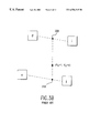
- FIGS. 1-4 further illustrate prior art hand-held scanning and image resampling.
- a hand-held scanner 100 is manually moved across the surface of a document 102 along a serpentine path 102 .
- FIGS. 2, 3 A and 3 B illustrate prior art resampling.
- FIG. 2 illustrates a scan-line 200 with image intensities measured at discrete points 202 along the scan-line. Also illustrated in FIG. 2 is a grid of pixel locations 204 . The lines of the pixel grid are ideally parallel to the sides of the document, but may be determined by the first scan-line as discussed above.
- Separate position sensors are used to measure the relative movement of the ends of the scan-line 200 .
- the position of each measured intensity 202 may be determined relative to the reference position.
- the measured intensities 202 and sufficient information to determine the position of each measured intensity 202 , may be stored in a memory for later rectification, or rectification may be computed in real time as the intensity data is generated.
- FIG. 3A illustrates a series of scan-lines ( 300 , 302 , 304 , 306 ) determined by the position of the linear sensor array of the scanner as the scanner is moved across the document being scanned. Each intensity measurement from the scanner sensor array has been assigned a lower-case letter.
- FIG. 3A also illustrates a grid of pixel locations. The pixel locations have been assigned location notations relative to an arbitrary reference location (X 0 , Y 0 ). To simplify illustration, in FIG. 3A, each scan-line has five photosensor elements and five intensity measurements. In a typical actual scanner, one linear sensor array may comprise thousands of individual photosensor elements.
- FIG. 3B illustrates one example method of computing intensities at the pixel locations from measured intensities from the scanner sensor array.
- One method for computing image rectification is bilinear interpolation using the intensities of the four closest neighboring sensor values. See, for example, Christopher D. Watkins, et al., Modern Image Processing: Warping, Morphing, and Classical Techniques , (Cambridge, Mass., Academic Press, 1993), pp. 99-102.
- FIG. 3 B A version of bilinear interpolation, as applied to FIG. 3A, is illustrated in FIG. 3 B. In FIG.
- the (X,Y) locations of sensor values (d), (e), (i), and (j), and the (X,Y) location of pixel (X 0 +1, Y 0 +4) are all known.
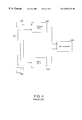
- FIG. 4 illustrates a simplified block diagram of a prior art system implementing a hand-held scanner in accordance with FIGS. 1, 2 , 3 A and 3 B.
- a linear image sensor array 400 measures intensities along a scan-line determined by the position of array 400 on a document being scanned.
- Position sensors 402 sense the relative movements of the ends of the sensor array 400 .
- a position data system 408 determines relative positions of the end-points of the scan-line.
- An image data system 406 receives analog intensity measurements from the linear sensor array 400 , and uses an analog-to-digital converter to convert the analog image values into numeric image values.
- a rectification system 408 receives position data from the position data system 404 and numeric image data from the image data system 406 and computes resampled pixel data.
- the position data system 404 may be a processor or may be specialized electronics.
- the position data and the image data may or may not be stored in a memory before being sent to the rectification system.
- the rectified image data generated by the rectification system is stored in Random Access Memory (RAM).
- photosensor segment alignment data such as segment position offset and segment angle
- the offset and angle are stored in non-volatile memory within the scanner.
- a position correction system uses the stored alignment data to correct position and angle values before being processed by a rectification system.
- Most pixels require simple geometry calculations. However, a more complex state machine is needed to handle the transition from one photosensor segment to the next. Correcting for segment position offset and angle errors enables a cost reduction for the sensor array and, in particular, reduces costs associated with scrap.
- FIG. 1 (prior art) is a perspective view of a hand-held scanner on a document.
- FIG. 2 (prior art) is a plan view of a scan-line on a pixel grid.
- FIG. 3A (prior art) is an expanded view of a pixel grid with multiple scan-lines.
- FIG. 3B (prior art) is an expanded view of one point on the pixel grid illustrating bilinear interpolation.
- FIG. 4 (prior art) is a simplified block diagram of a hand-held scanner system.
- FIG. 5 (prior art) is a block diagram of an example ideal segmented sensor array.
- FIG. 6A is a block diagram of a segmented sensor array with imprecise alignment.
- FIG. 6B is a expanded view of part of FIG. 6A illustrating the geometric relationship between an ideal position for a photosensor element and an actual position for a photosensor element.
- FIG. 7 is a block diagram of part of a scanner system in accordance with an example embodiment of the invention.
- FIG. 8 is an expanded view of a pixel grid with offset segments as in FIG. 6 A.
- FIG. 9A is a flow chart of method for transition between segments, in accordance with an example embodiment of the invention.
- FIG. 9B is a flow chart illustrating additional detail for part of the method of FIG. 9 A.
- FIG. 5 illustrates an example of an ideal segmented sensor array.
- a first segment 500 has multiple photosensor elements ( 504 - 506 ).
- a second segment 502 has multiple photosensor elements ( 508 - 510 ).
- segment 500 be segment number one
- element 504 be photosensor element number one for segment number one
- photosensor element 504 is photosensor element ( 1 , 1 )
- photosensor element 506 is photosensor element ( 1 ,N)
- photosensor element 508 is photosensor element ( 2 , 1 )
- photosensor element 510 is photosensor element ( 2 ,N).
- broken square 512 depicts an image area for which light is not captured by the photosensor elements.
- One simple approach to provide image data for image area 512 is to assign to area 512 the average value of the intensity values measured by photosensor elements ( 1 ,N) and ( 2 , 1 ).
- the segmented sensor array in FIG. 5 is assumed to be ideal. Given the (X,Y) position of photosensor ( 1 , 1 ) (where (X,Y) refer to a pixel grid as in FIGS. 2, and 3 A), and given the slope of the sensor array in the (X,Y) coordinate space, the (X,Y) position of any photosensor is easily determined from its segment number and photosensor number.
- FIG. 6A illustrates a segmented array in which the segments are not perfectly aligned.
- the misalignment is exaggerated in FIG. 6A to facilitate illustration.
- a first segment 600 has multiple photosensor elements ( 604 - 606 ).
- a second segment 602 has multiple photosensor elements ( 608 - 610 ).
- a reference line 612 defines an ideal scan-line. Line 612 may be defined, for example, by connecting the center of the first photosensor element of the first segment to the center of the last photosensor element of the last segment. Alternatively, reference line 612 may be defined statistically, for example, as a least squares fit through the set of all photosensor elements. Given a reference line, direction L is along the reference line, and direction K is perpendicular to the reference line.
- Line 614 connects the centers of the photosensors of the first segment. That is, line 614 represents the slope of segment 600 . Areas 616 and 618 depict image areas, between the first and second segments, resulting from an extrapolation along line 614 of the image areas sensed by the photosensor elements of the first segment ( 600 ). Likewise, areas 620 and 622 depict image areas, between the first and second segments, resulting from an extrapolation of the areas sensed by the photosensor elements of the second segment ( 602 ). There is an ideal location along reference line 612 for each photosensor element, for example, as if an ideal segmented array, as illustrated in FIG. 5, was aligned along reference line 612 .
- Dot 624 on reference line 612 depicts the ideal location for photosensor element 604 . If the segments were perfectly aligned as in FIG. 5, area 620 would be identical to area 606 , area 618 would be identical to area 608 , and area 616 would be identical to area 622 .
- the alignment of each of the segments of the photosensor array is measured, and alignment data is stored in non-volatile memory within the scanner.
- the photosensor array is used to scan a known calibration target. From the resulting image data, segment offsets and angles are measured.
- An example of suitable alignment data, for each segment is as follows.
- transition bit one transition bit for each gap between segments, indicating, for example, whether two adjacent ends are more than one pixel apart in the K dimension.
- the example alignment data for segment 600 would be: the distance in the L and K dimensions between the ideal position 624 and the actual position of photosensor element 604 ; the slope in (L,K) coordinate space of line 614 ; and a transition bit that is not set, indicating that the ends of segments 600 and 602 are not more than one pixel apart in the K dimension.
- FIG. 6B is an expanded view of portions of FIG. 6A illustrating the geometry required for computing the (X,Y) location of the first photosensor element of each segment, and ⁇ X and ⁇ Y between photosensor elements for each segment.
- lines 612 and 614 are as defined in FIG. 6 A.
- dimension L is parallel to reference line 612
- dimension K is orthogonal to reference line 612 .
- Reference line 612 has a known slope in (X,Y) coordinate space.
- the (X,Y) coordinates of the ideal position of the first photosensor element of each element may be computed by simple addition as discussed above.
- Point A is the ideal location for the first photosensor element of a segment
- point B is the actual position.
- point A is the location of a photosensor element given aligned segments as in FIG. 5 .
- Distance AC and distance CB are known from the calibration data ( ⁇ L and ⁇ K, respectively).
- the (X,Y) position of actual point B is unknown, and must be computed by an error correction system.
- Line CB is perpendicular to reference line 612 . Given the (X,Y) location of point A, the slope of line 612 in (X,Y) coordinate space, and the distance AC ( ⁇ L), the (X,Y) location of point C is determined. Given the (X,Y) location of point C, the slope of line CB in (X,Y) coordinate space, and distance CB ( ⁇ K), the (X,Y) location of point B is determined.
- the correction system must also compute the slope of line 614 in (X,Y) coordinate space. More precisely, the correction system must provide ⁇ X and ⁇ Y values used to incrementally compute the (X,Y) position of each image area.
- the slope of line 614 relative to line 612 is known from the alignment data. Given the slope of line 612 , the slope of line 614 is computed by a simple linear equation, as given below in conjunction with a discussion of FIG. 7 . As will be discussed further below, the correction system must also calculate transition image areas between segments.
- FIG. 7 illustrates part of the block diagram of FIG. 4, with example modifications suitable for implementing the invention.
- the position data system 404 , the image data system 406 , and the rectification system 408 may all be as implemented in FIG. 4 .
- alignment data 700 is determined at manufacturing time and saved in a non-volatile memory 702 .
- position data for the first element of each segment, and the slope of each segment are then corrected by the error correction system 704 before being sent to the rectification system 408 .
- the error correction system 704 and the rectification system 408 are illustrated as two separate functional blocks in FIG. 7, they are preferably physically combined as part of one Application Specific Integrated Circuit (ASIC).
- ASIC Application Specific Integrated Circuit
- the rectification system 408 receives the following position data from the position data system 404 .
- the error correction system 704 receives the above information, and in addition receives the following information, on a segment-by-segment basis, from the non-volatile memory 702 .
- TranBit Transition Bit a bit used for deciding which data to use for the transition from one segment to the next.
- the error correction system 704 then computes the following equations (where S is segment number):
- dX/dY SEGMENT dX/dY REFERENCE +( dK/dL ) SEGMENT *( dL/dY ) REFERENCE
- the intensity assigned to area 524 may be a average of the intensities measured by photosensors 512 and 514 .
- misaligned segments may be shifted in both the L and K dimensions by more than one pixel (where “pixel” in this sense refers to the pitch of the photosensor elements).
- pixel in this sense refers to the pitch of the photosensor elements.
- other approaches have been found to be more suitable for reducing visual artifacts.
- the following example method rather than one intermediate computed area, as depicted in FIG.
- FIG. 8 depicts areas 606 , 616 , 618 , 620 , 622 , and 608 (all from FIG. 6A) on an (X,Y) grid as in FIG. 3 A.
- the black squares depict areas corresponding to actual photosensor elements, and the white squares depict extrapolated areas.
- the black circle 800 depicts an (X,Y) grid point to be used for rectification computation. In the following example method, only two of the computed areas (either 616 and 618 , or 620 and 622 ) will be used for rectification computation.
- the rectification system receives image data (intensity values) and (X,Y) locations (position data) for the intensity values. More precisely, the rectification system 408 receives an integer index value which is used as an index for a list of intensity values, and receives (X,Y) position data for each index value.
- the term “average intensity” means the average of the intensity of the last actual area for one segment and the intensity of the first actual area of the next segment. In the system of FIG. 4, for each transition between segments, one computed intensity entry with the average intensity value is inserted and stored as part of the image data 406 being sent to the rectification module 408 .
- N actual intensity values per segment there are N+2 intensity values associated with each segment, numbered zero through (N+1).
- an index value of (1) points to the first actual intensity for the segment and an index value of (0) points to an average intensity.
- an index value of (N) points to the last actual intensity value of the segment, and an index value of (N+1) points to an average intensity.
- Element (N+1) for one segment, and element (0) for the next segment correspond to the same intensity entry in a table of intensity values, but the two computed areas may have different (X,Y) locations, as illustrated in FIG. 8 .
- An algorithm within the position correction system decides whether to send to the rectification system (FIG. 7, 408 ), the (X,Y) locations of areas 616 and 618 , or the (X,Y) locations of areas 620 and 622 , and which intensity values from the table of intensity values should be assigned to each area.
- FIG. 9A is an example of an overall method for correcting for segment misalignment, and in particular an example of a method for choosing image areas and intensities during the transition between segments.
- the following assumptions and definitions are applicable:
- SEGMENT is an integer segment number.
- A is a position indicator along the length of the array.
- A(SEG) is the variable “A” within a segment (nominal range is 1 to (N+1)).
- the transition bit is set (during calibration) if the beginning of one segment is displaced relative to the end of the previous segment, in the K dimension, by at least one pixel.
- FIG. 9A illustrates an overview for an example method to compute corrected (X,Y) values within segments and to determine appropriate transition pixels between segments.
- the method progresses in uniform increments in the Y dimension.
- Variable “A” is incremented by a value (dL/dY) corresponding to the distance moved in the L dimension when Y is incremented from one pixel to the next.
- the rectification module processes pixel values in pairs (for example, d,e, and i,j). Therefore, each pass through the loop illustrated in FIG. 9A determines two corrected sensor positions for use in rectification.
- the variable “A” identifies the two pixel values that are appropriate for each value of Y. For example, in FIG.
- variable “A”, as used in FIG. 9A, at some point may have, for example, a value of 4.8, indicating that for pixel (X 0 +1, Y 0 +4), the two appropriate photosensor values are the fourth and fifth entries in a table or list of intensity values.
- values for SEGMENT, and “A” are initialized.
- A(SEG) is computed.
- decision 904 a decision is made as to whether or not it is time to switch to a new segment. Steps 902 and 904 are discussed in more detail below. If A(SEG) minus half the value of EL for the next segment is greater than (N+1), then the method switches to a new segment (step 916 ). If, at decision 904 , it is time to switch segments, then at step 916 , SEGMENT and other segment specific variables are updated.
- the value of (X,Y) for each of the next two photosensor elements is computed (two values are computed).
- step 906 is provided in FIG. 9 B.
- the position correction system (FIG. 7, 704 ) sends two INDEX values (INDEX 1 , INDEX 2 ) and two corrected (X,Y) positions to the rectification system (FIG. 7, 408 ).
- step 910 “A” is incremented.
- steps 902 and 904 for purposes of illustration, assume that EL for each of two consecutive segments has a magnitude of one (shifted by one pixel).
- a positive EL means that a segment is shifted toward the bottom of the figure. If the segments are perfectly aligned, then the method should switch segments when A(SEG) exceeds (N+1). If the first segment has an EL of positive one, and if the second segment has an EL of positive one, then both segments are shifted, but the spacing in the L dimension between their ends is perfect. At step 904 , the segments will be switched when A(SEG) exceeds (N+1).
- the ends of the segments are far apart.
- A(SEG) will start at zero.
- the segments will be switched when A(SEG) exceeds (N). Effectively, the decision to switch segments is made early.
- FIG. 9B provides more detail for step 906 in FIG. 9 A. If the process is not in a transition zone, then index values are selected in step 962 . If the process is in a transition zone, and if the end of an old segment is extrapolated into the transition zone, then index values are specified in steps 928 , 930 , 936 or 938 . If the process is in a transition zone, and if the beginning of a new segment is extrapolated, then index values are specified in steps 948 , 950 , 956 , or 958 .
- first segment has an EL of negative one
- second segment has an EL of positive one
- the ends of the segments are far apart in the L dimension
- A(SEG) will equal N+2 when the decision is made to switch segments.
- the positions of the two transition elements are extrapolated from the first segment (FIG. 8, elements 616 and 618 ). If the transition bit is set, the ends are far apart both in the L dimension and in the K dimension. This is approximately the situation illustrated in FIG. 8, where the ends are far apart in the L dimension (elements 616 and 622 should be aligned in the L dimension) and in the K dimension (elements 606 and 608 should be aligned in the K dimension).
- elements 620 , 622 and 608 should be even further to the right. If the transition bit is set, it is reasonable to increase the contribution of element 606 , so the intensity of real element 606 is used for computed element 616 and the average intensity value is used for computed element 618 (FIG. 9B, step 928 ). If the transition bit is not set, then it is reasonable to balance the contribution of elements 606 and 608 , so the average intensity is used for elements 616 and 618 (FIG. 9B, step 930 ).
- a first segment has an EL of one
- a second segment has an EL of negative one (the ends overlap in the L dimension).
- the positions of the two transition elements are extrapolated from the second segment (FIG. 8, elements 620 and 622 ). If the transition bit is set, then it is reasonable to increase the contribution of real element 608 (FIG. 8 ), so the intensity of real element 608 is used for computed element 622 , and the average intensity is used for element 620 (FIG. 9B, step 948 ). If the transition bit is not set, then it is reasonable to balance the contribution of elements 606 and 608 , and the average intensity value is used for elements 620 and 622 (FIG. 9B, step 950 ).
- both the first and second extrapolated areas are assigned the intensity of the last actual area of the previous segment. If the transition bit is not set (decision 934 ), then in step 938 the first extrapolated area is assigned the intensity of the last actual area of the previous segment, and the second extrapolated area is assigned the average intensity.
- A(SEG) is less than zero (decision 944 ), or if A(SEG) is less than one (decision 952 ), then two computed areas are extrapolated from the new segment. If A(SEG) is less than zero, and the transition bit is set (decision 946 ), then at step 948 the first extrapolated area is assigned the average intensity, and the second extrapolated area is assigned the intensity of the first actual area of the new segment. If the transition bit is not set (decision 946 ), then both extrapolated areas are assigned the average intensity.
- both extrapolated areas are assigned the intensity of the first actual area of the new segment. If the transition bit is not set (decision 954 ) then at step 958 the first extrapolated area is assigned the average intensity, and the second extrapolated area is assigned the intensity of the first actual area of the new segment. If A(SEG) is greater than or equal to one and less than or equal to N, then the process is not in a transition zone and index values are specified by step 962 .
- the system described above is just one example of correcting for misaligned segments.
- the characterization of the error correction system as a separate entity, or the characterization of the position data system as a separate entity is only to facilitate explanation of functions.
- the alignment data could be presented directly to the position data system and the position data system could provide corrected data directly to a rectification system.
- a correction system could receive raw data from the position sensors, and send corrected data to the position data system.
- the offset of the first photosensor element and slope instead of measuring the offset of the first photosensor element and slope, the offset of the first and last photosensor elements of each segment could be measured. Instead of measuring the offset of one or both ends of a segment, the offset of every photosensor element could be measured.
- the use of a transition bit, and the criteria for setting the transition bit is just one example of an algorithm for selecting transition pixel intensities.
Landscapes
- Engineering & Computer Science (AREA)
- Health & Medical Sciences (AREA)
- Biomedical Technology (AREA)
- General Health & Medical Sciences (AREA)
- Multimedia (AREA)
- Signal Processing (AREA)
- Facsimile Scanning Arrangements (AREA)
- Image Input (AREA)
Priority Applications (2)
| Application Number | Priority Date | Filing Date | Title |
|---|---|---|---|
| US09/365,112 US6556315B1 (en) | 1999-07-30 | 1999-07-30 | Digital image scanner with compensation for misalignment of photosensor array segments |
| JP2000217269A JP2001053939A (ja) | 1999-07-30 | 2000-07-18 | 光センサアレイセグメントの位置ずれ補正機能を有するディジタルイメージスキャナ |
Applications Claiming Priority (1)
| Application Number | Priority Date | Filing Date | Title |
|---|---|---|---|
| US09/365,112 US6556315B1 (en) | 1999-07-30 | 1999-07-30 | Digital image scanner with compensation for misalignment of photosensor array segments |
Publications (1)
| Publication Number | Publication Date |
|---|---|
| US6556315B1 true US6556315B1 (en) | 2003-04-29 |
Family
ID=23437511
Family Applications (1)
| Application Number | Title | Priority Date | Filing Date |
|---|---|---|---|
| US09/365,112 Expired - Fee Related US6556315B1 (en) | 1999-07-30 | 1999-07-30 | Digital image scanner with compensation for misalignment of photosensor array segments |
Country Status (2)
| Country | Link |
|---|---|
| US (1) | US6556315B1 (enExample) |
| JP (1) | JP2001053939A (enExample) |
Cited By (18)
| Publication number | Priority date | Publication date | Assignee | Title |
|---|---|---|---|---|
| US20040120017A1 (en) * | 2002-12-20 | 2004-06-24 | Miller Mindy Lee | Method and apparatus for compensating for assembly and alignment errors in sensor assemblies |
| WO2005041281A1 (en) * | 2003-10-22 | 2005-05-06 | Northrop Grumman Corporation | Hard substrate wafer sawing process |
| US20060061613A1 (en) * | 2004-09-21 | 2006-03-23 | Z Corporation | Apparatus and methods for servicing 3D printers |
| US20060141145A1 (en) * | 1996-12-20 | 2006-06-29 | Z Corporation | Three-dimensional printer |
| US20070126157A1 (en) * | 2005-12-02 | 2007-06-07 | Z Corporation | Apparatus and methods for removing printed articles from a 3-D printer |
| US20080042321A1 (en) * | 2003-05-23 | 2008-02-21 | Z Corporation | Apparatus and Methods for 3D Printing |
| US20080060330A1 (en) * | 2006-05-26 | 2008-03-13 | Z Corporation | Apparatus and methods for handling materials in a 3-D printer |
| US20080252682A1 (en) * | 2004-09-21 | 2008-10-16 | Z Corporation | Apparatus and Methods for Servicing 3D Printers |
| US20090011066A1 (en) * | 1996-12-20 | 2009-01-08 | Z Corporation | Three-Dimensional Printer |
| US20110134491A1 (en) * | 2009-12-09 | 2011-06-09 | Xerox Corporation | Duplexing document handler with defect reduction |
| US8040555B1 (en) * | 2007-02-15 | 2011-10-18 | Marvell International Ltd. | Method and apparatus for processing image data for an irregular output scan path |
| US20150199591A1 (en) * | 2012-08-21 | 2015-07-16 | Cognex Corporation | Trainable Handheld Optical Character Recognition Systems and Methods |
| US10068153B2 (en) | 2012-08-21 | 2018-09-04 | Cognex Corporation | Trainable handheld optical character recognition systems and methods |
| CN109146865A (zh) * | 2018-08-22 | 2019-01-04 | 成都新西旺自动化科技有限公司 | 一种视觉对位检测图源生成系统 |
| CN109819137A (zh) * | 2017-11-22 | 2019-05-28 | 东友科技股份有限公司 | 影像获取与输出方法 |
| EP3490238A1 (en) * | 2017-11-22 | 2019-05-29 | Teco Image Systems Co., Ltd. | Image capture and output method |
| US10356385B2 (en) * | 2016-06-07 | 2019-07-16 | Stock Company Research and Development Center “Electronic Information Computation Systems” | Method and device for stereo images processing |
| US11061351B2 (en) * | 2019-01-09 | 2021-07-13 | Canon Kabushiki Kaisha | Measuring device and image forming apparatus |
Families Citing this family (1)
| Publication number | Priority date | Publication date | Assignee | Title |
|---|---|---|---|---|
| US6556315B1 (en) * | 1999-07-30 | 2003-04-29 | Hewlett-Packard Company | Digital image scanner with compensation for misalignment of photosensor array segments |
Citations (7)
| Publication number | Priority date | Publication date | Assignee | Title |
|---|---|---|---|---|
| US5578813A (en) | 1995-03-02 | 1996-11-26 | Allen; Ross R. | Freehand image scanning device which compensates for non-linear movement |
| US5619345A (en) | 1990-07-26 | 1997-04-08 | Seiko Instruments Inc. | Linear image sensor of the contact type |
| US5729008A (en) | 1996-01-25 | 1998-03-17 | Hewlett-Packard Company | Method and device for tracking relative movement by correlating signals from an array of photoelements |
| JP2001053939A (ja) * | 1999-07-30 | 2001-02-23 | Hewlett Packard Co <Hp> | 光センサアレイセグメントの位置ずれ補正機能を有するディジタルイメージスキャナ |
| US6207945B1 (en) * | 1999-06-30 | 2001-03-27 | Hewlett-Packard Company | Integral positioning and imaging device |
| US6242731B1 (en) * | 1999-06-30 | 2001-06-05 | Hewlett Packard Company | Imaging device having an integrated position sensing device |
| US6346699B1 (en) * | 2000-01-04 | 2002-02-12 | Hewlett-Packard Company | Optical assembly having a reduced width |
-
1999
- 1999-07-30 US US09/365,112 patent/US6556315B1/en not_active Expired - Fee Related
-
2000
- 2000-07-18 JP JP2000217269A patent/JP2001053939A/ja active Pending
Patent Citations (8)
| Publication number | Priority date | Publication date | Assignee | Title |
|---|---|---|---|---|
| US5619345A (en) | 1990-07-26 | 1997-04-08 | Seiko Instruments Inc. | Linear image sensor of the contact type |
| US5578813A (en) | 1995-03-02 | 1996-11-26 | Allen; Ross R. | Freehand image scanning device which compensates for non-linear movement |
| US5644139A (en) | 1995-03-02 | 1997-07-01 | Allen; Ross R. | Navigation technique for detecting movement of navigation sensors relative to an object |
| US5729008A (en) | 1996-01-25 | 1998-03-17 | Hewlett-Packard Company | Method and device for tracking relative movement by correlating signals from an array of photoelements |
| US6207945B1 (en) * | 1999-06-30 | 2001-03-27 | Hewlett-Packard Company | Integral positioning and imaging device |
| US6242731B1 (en) * | 1999-06-30 | 2001-06-05 | Hewlett Packard Company | Imaging device having an integrated position sensing device |
| JP2001053939A (ja) * | 1999-07-30 | 2001-02-23 | Hewlett Packard Co <Hp> | 光センサアレイセグメントの位置ずれ補正機能を有するディジタルイメージスキャナ |
| US6346699B1 (en) * | 2000-01-04 | 2002-02-12 | Hewlett-Packard Company | Optical assembly having a reduced width |
Non-Patent Citations (2)
| Title |
|---|
| "Modern Image Processing: Warping, Morphing, and Classical Techniques" Christopher D. Watkins, Alberto Sadum, Stephen Marenka Academic Press Professional, A Division of Harcourt Brace & Company, Boston, MA 1993. |
| Hewlett-Packard Co., "Digital Image Scanner With Optical Sensor Segments . . . ", Derwent-Acc-No: 2002-063779, 1999.* * |
Cited By (37)
| Publication number | Priority date | Publication date | Assignee | Title |
|---|---|---|---|---|
| US20090011066A1 (en) * | 1996-12-20 | 2009-01-08 | Z Corporation | Three-Dimensional Printer |
| US7435368B2 (en) | 1996-12-20 | 2008-10-14 | Z Corporation | Three-dimensional printer |
| US8017055B2 (en) | 1996-12-20 | 2011-09-13 | Z Corporation | Three-dimensional printer |
| US20060141145A1 (en) * | 1996-12-20 | 2006-06-29 | Z Corporation | Three-dimensional printer |
| US20100151136A1 (en) * | 1996-12-20 | 2010-06-17 | Z Corporation | Three-Dimensional Printer |
| US7686995B2 (en) | 1996-12-20 | 2010-03-30 | Z Corporation | Three-dimensional printer |
| US20040120017A1 (en) * | 2002-12-20 | 2004-06-24 | Miller Mindy Lee | Method and apparatus for compensating for assembly and alignment errors in sensor assemblies |
| US20080042321A1 (en) * | 2003-05-23 | 2008-02-21 | Z Corporation | Apparatus and Methods for 3D Printing |
| WO2005041281A1 (en) * | 2003-10-22 | 2005-05-06 | Northrop Grumman Corporation | Hard substrate wafer sawing process |
| US8167395B2 (en) | 2004-09-21 | 2012-05-01 | 3D Systems, Inc. | Apparatus and methods for servicing 3D printers |
| US20080252682A1 (en) * | 2004-09-21 | 2008-10-16 | Z Corporation | Apparatus and Methods for Servicing 3D Printers |
| US7824001B2 (en) | 2004-09-21 | 2010-11-02 | Z Corporation | Apparatus and methods for servicing 3D printers |
| US20060061613A1 (en) * | 2004-09-21 | 2006-03-23 | Z Corporation | Apparatus and methods for servicing 3D printers |
| US20110032301A1 (en) * | 2004-09-21 | 2011-02-10 | Z Corporation | Apparatus and methods for servicing 3d printers |
| US20070126157A1 (en) * | 2005-12-02 | 2007-06-07 | Z Corporation | Apparatus and methods for removing printed articles from a 3-D printer |
| US20110211016A1 (en) * | 2006-05-26 | 2011-09-01 | Z Corporation | Apparatus and methods for handling materials in a 3-d printer |
| US7971991B2 (en) | 2006-05-26 | 2011-07-05 | Z Corporation | Apparatus and methods for handling materials in a 3-D printer |
| US7979152B2 (en) | 2006-05-26 | 2011-07-12 | Z Corporation | Apparatus and methods for handling materials in a 3-D printer |
| US7828022B2 (en) | 2006-05-26 | 2010-11-09 | Z Corporation | Apparatus and methods for handling materials in a 3-D printer |
| US20110233808A1 (en) * | 2006-05-26 | 2011-09-29 | Z Corporation | Apparatus and methods for handling materials in a 3-d printer |
| US20080060330A1 (en) * | 2006-05-26 | 2008-03-13 | Z Corporation | Apparatus and methods for handling materials in a 3-D printer |
| US8185229B2 (en) | 2006-05-26 | 2012-05-22 | 3D Systems, Inc. | Apparatus and methods for handling materials in a 3-D printer |
| US8040555B1 (en) * | 2007-02-15 | 2011-10-18 | Marvell International Ltd. | Method and apparatus for processing image data for an irregular output scan path |
| US8405880B1 (en) * | 2007-02-15 | 2013-03-26 | Marvell International Ltd. | Method and apparatus for processing image data for an irregular output scan path |
| US20110134491A1 (en) * | 2009-12-09 | 2011-06-09 | Xerox Corporation | Duplexing document handler with defect reduction |
| US8467107B2 (en) * | 2009-12-09 | 2013-06-18 | Xerox Corporation | Duplexing document handler with defect reduction |
| US20150199591A1 (en) * | 2012-08-21 | 2015-07-16 | Cognex Corporation | Trainable Handheld Optical Character Recognition Systems and Methods |
| US9767384B2 (en) * | 2012-08-21 | 2017-09-19 | Cognex Corporation | Trainable handheld optical character recognition systems and methods |
| US10068153B2 (en) | 2012-08-21 | 2018-09-04 | Cognex Corporation | Trainable handheld optical character recognition systems and methods |
| US10356385B2 (en) * | 2016-06-07 | 2019-07-16 | Stock Company Research and Development Center “Electronic Information Computation Systems” | Method and device for stereo images processing |
| CN109819137A (zh) * | 2017-11-22 | 2019-05-28 | 东友科技股份有限公司 | 影像获取与输出方法 |
| EP3490238A1 (en) * | 2017-11-22 | 2019-05-29 | Teco Image Systems Co., Ltd. | Image capture and output method |
| US10341522B2 (en) | 2017-11-22 | 2019-07-02 | Teco Image Systems Co., Ltd. | Image capture and output method |
| CN109819137B (zh) * | 2017-11-22 | 2020-06-26 | 东友科技股份有限公司 | 影像获取与输出方法 |
| CN109146865A (zh) * | 2018-08-22 | 2019-01-04 | 成都新西旺自动化科技有限公司 | 一种视觉对位检测图源生成系统 |
| US11061351B2 (en) * | 2019-01-09 | 2021-07-13 | Canon Kabushiki Kaisha | Measuring device and image forming apparatus |
| US11835901B2 (en) | 2019-01-09 | 2023-12-05 | Canon Kabushiki Kaisha | Measuring device and image forming apparatus |
Also Published As
| Publication number | Publication date |
|---|---|
| JP2001053939A (ja) | 2001-02-23 |
Similar Documents
| Publication | Publication Date | Title |
|---|---|---|
| US6556315B1 (en) | Digital image scanner with compensation for misalignment of photosensor array segments | |
| US6771396B1 (en) | Document imaging system | |
| EP1343332B1 (en) | Stereoscopic image characteristics examination system | |
| US6288801B1 (en) | Self calibrating scanner with single or multiple detector arrays and single or multiple optical systems | |
| US6600568B1 (en) | System and method of measuring image sensor chip shift | |
| JP2021061563A (ja) | 画像読取装置、その制御方法、及びプログラム | |
| US5990470A (en) | Scanner system and method for automatically compensating main-scan and sub-scan sensor positioning errors | |
| US6201619B1 (en) | Autofocus process and system with fast multi-region sampling | |
| JP6163946B2 (ja) | 画像処理装置 | |
| JP2000175001A (ja) | 画像読取り装置における画像データ補正方法 | |
| CN116309063A (zh) | 校正信息生成方法、图像拼接方法与装置及图像采集系统 | |
| US20040120017A1 (en) | Method and apparatus for compensating for assembly and alignment errors in sensor assemblies | |
| EP4456521B1 (en) | A scanning device | |
| CN1161960C (zh) | 多电荷耦合元件校正装置 | |
| JPH05172531A (ja) | 距離計測方法 | |
| Gruber et al. | Novel high precision photogrammetric scanning | |
| JP2522706B2 (ja) | ラインセンサの接続偏差検出方法 | |
| EP0526070A2 (en) | Apparatus and method for determining geometrical parameters of an optical system | |
| JP6544233B2 (ja) | 画像読取装置のキャリブレーション方法及び画像読取装置 | |
| JP2002374392A (ja) | 画像位置ずれ計測装置、画像位置ずれ計測方法およびその方法によったプログラムを記憶した記憶媒体 | |
| EP1096783A1 (en) | Document imaging system | |
| JPH0619247B2 (ja) | 物体の端部位置測定装置 | |
| CN1167251C (zh) | 一种多电荷耦合元件校正装置 | |
| JP2002314769A (ja) | 画像読取装置 | |
| JPH0888778A (ja) | 画像走査装置 |
Legal Events
| Date | Code | Title | Description |
|---|---|---|---|
| AS | Assignment |
Owner name: HEWLETT-PACKARD COMPANY, COLORADO Free format text: ASSIGNMENT OF ASSIGNORS INTEREST;ASSIGNORS:KOMMRUSCH, STEVEN J.;CRANE, RANDY T.;REEL/FRAME:010389/0797 Effective date: 19990914 |
|
| AS | Assignment |
Owner name: HEWLETT-PACKARD DEVELOPMENT COMPANY, L.P., TEXAS Free format text: ASSIGNMENT OF ASSIGNORS INTEREST;ASSIGNOR:HEWLETT-PACKARD COMPANY;REEL/FRAME:013862/0623 Effective date: 20030728 |
|
| FPAY | Fee payment |
Year of fee payment: 4 |
|
| FPAY | Fee payment |
Year of fee payment: 8 |
|
| REMI | Maintenance fee reminder mailed | ||
| LAPS | Lapse for failure to pay maintenance fees | ||
| STCH | Information on status: patent discontinuation |
Free format text: PATENT EXPIRED DUE TO NONPAYMENT OF MAINTENANCE FEES UNDER 37 CFR 1.362 |
|
| FP | Lapsed due to failure to pay maintenance fee |
Effective date: 20150429 |