US6509109B1 - Organic electroluminescent device - Google Patents

Organic electroluminescent device Download PDF

Info

Publication number
US6509109B1
US6509109B1 US09/281,953 US28195399A US6509109B1 US 6509109 B1 US6509109 B1 US 6509109B1 US 28195399 A US28195399 A US 28195399A US 6509109 B1 US6509109 B1 US 6509109B1
Authority
US
United States
Prior art keywords
electron injection
injection region
organic electroluminescent
electroluminescent device
electron
Prior art date
Legal status (The legal status is an assumption and is not a legal conclusion. Google has not performed a legal analysis and makes no representation as to the accuracy of the status listed.)
Expired - Lifetime
Application number
US09/281,953
Inventor
Hiroaki Nakamura
Chishio Hosokawa
Kenichi Fukuoka
Hiroshi Tokailin
Current Assignee (The listed assignees may be inaccurate. Google has not performed a legal analysis and makes no representation or warranty as to the accuracy of the list.)
Idemitsu Kosan Co Ltd
Original Assignee
Idemitsu Kosan Co Ltd
Priority date (The priority date is an assumption and is not a legal conclusion. Google has not performed a legal analysis and makes no representation as to the accuracy of the date listed.)
Filing date
Publication date
Family has litigation
First worldwide family litigation filed litigation Critical https://patents.darts-ip.com/?family=27308037&utm_source=google_patent&utm_medium=platform_link&utm_campaign=public_patent_search&patent=US6509109(B1) "Global patent litigation dataset” by Darts-ip is licensed under a Creative Commons Attribution 4.0 International License.
Application filed by Idemitsu Kosan Co Ltd filed Critical Idemitsu Kosan Co Ltd
Assigned to IDEMITSU KOSAN CO., LTD. reassignment IDEMITSU KOSAN CO., LTD. ASSIGNMENT OF ASSIGNORS INTEREST (SEE DOCUMENT FOR DETAILS). Assignors: FUKUOKA, KENICHI, HOSOKAWA, CHISHIO, NAKAMURA, HIROAKI, TOKAILIN, HIROSHI
Application granted granted Critical
Publication of US6509109B1 publication Critical patent/US6509109B1/en
Anticipated expiration legal-status Critical
Expired - Lifetime legal-status Critical Current

Links

Images

Classifications

    • HELECTRICITY
    • H10SEMICONDUCTOR DEVICES; ELECTRIC SOLID-STATE DEVICES NOT OTHERWISE PROVIDED FOR
    • H10KORGANIC ELECTRIC SOLID-STATE DEVICES
    • H10K71/00Manufacture or treatment specially adapted for the organic devices covered by this subclass
    • H10K71/30Doping active layers, e.g. electron transporting layers
    • CCHEMISTRY; METALLURGY
    • C09DYES; PAINTS; POLISHES; NATURAL RESINS; ADHESIVES; COMPOSITIONS NOT OTHERWISE PROVIDED FOR; APPLICATIONS OF MATERIALS NOT OTHERWISE PROVIDED FOR
    • C09KMATERIALS FOR MISCELLANEOUS APPLICATIONS, NOT PROVIDED FOR ELSEWHERE
    • C09K11/00Luminescent, e.g. electroluminescent, chemiluminescent materials
    • C09K11/06Luminescent, e.g. electroluminescent, chemiluminescent materials containing organic luminescent materials
    • HELECTRICITY
    • H10SEMICONDUCTOR DEVICES; ELECTRIC SOLID-STATE DEVICES NOT OTHERWISE PROVIDED FOR
    • H10KORGANIC ELECTRIC SOLID-STATE DEVICES
    • H10K50/00Organic light-emitting devices
    • H10K50/10OLEDs or polymer light-emitting diodes [PLED]
    • H10K50/11OLEDs or polymer light-emitting diodes [PLED] characterised by the electroluminescent [EL] layers
    • HELECTRICITY
    • H10SEMICONDUCTOR DEVICES; ELECTRIC SOLID-STATE DEVICES NOT OTHERWISE PROVIDED FOR
    • H10KORGANIC ELECTRIC SOLID-STATE DEVICES
    • H10K50/00Organic light-emitting devices
    • H10K50/10OLEDs or polymer light-emitting diodes [PLED]
    • H10K50/17Carrier injection layers
    • H10K50/171Electron injection layers
    • HELECTRICITY
    • H10SEMICONDUCTOR DEVICES; ELECTRIC SOLID-STATE DEVICES NOT OTHERWISE PROVIDED FOR
    • H10KORGANIC ELECTRIC SOLID-STATE DEVICES
    • H10K2102/00Constructional details relating to the organic devices covered by this subclass
    • H10K2102/10Transparent electrodes, e.g. using graphene
    • H10K2102/101Transparent electrodes, e.g. using graphene comprising transparent conductive oxides [TCO]
    • H10K2102/103Transparent electrodes, e.g. using graphene comprising transparent conductive oxides [TCO] comprising indium oxides, e.g. ITO
    • HELECTRICITY
    • H10SEMICONDUCTOR DEVICES; ELECTRIC SOLID-STATE DEVICES NOT OTHERWISE PROVIDED FOR
    • H10KORGANIC ELECTRIC SOLID-STATE DEVICES
    • H10K85/00Organic materials used in the body or electrodes of devices covered by this subclass
    • H10K85/30Coordination compounds
    • H10K85/321Metal complexes comprising a group IIIA element, e.g. Tris (8-hydroxyquinoline) gallium [Gaq3]
    • H10K85/324Metal complexes comprising a group IIIA element, e.g. Tris (8-hydroxyquinoline) gallium [Gaq3] comprising aluminium, e.g. Alq3
    • HELECTRICITY
    • H10SEMICONDUCTOR DEVICES; ELECTRIC SOLID-STATE DEVICES NOT OTHERWISE PROVIDED FOR
    • H10KORGANIC ELECTRIC SOLID-STATE DEVICES
    • H10K85/00Organic materials used in the body or electrodes of devices covered by this subclass
    • H10K85/60Organic compounds having low molecular weight
    • H10K85/615Polycyclic condensed aromatic hydrocarbons, e.g. anthracene
    • H10K85/626Polycyclic condensed aromatic hydrocarbons, e.g. anthracene containing more than one polycyclic condensed aromatic rings, e.g. bis-anthracene
    • HELECTRICITY
    • H10SEMICONDUCTOR DEVICES; ELECTRIC SOLID-STATE DEVICES NOT OTHERWISE PROVIDED FOR
    • H10KORGANIC ELECTRIC SOLID-STATE DEVICES
    • H10K85/00Organic materials used in the body or electrodes of devices covered by this subclass
    • H10K85/60Organic compounds having low molecular weight
    • H10K85/631Amine compounds having at least two aryl rest on at least one amine-nitrogen atom, e.g. triphenylamine
    • H10K85/633Amine compounds having at least two aryl rest on at least one amine-nitrogen atom, e.g. triphenylamine comprising polycyclic condensed aromatic hydrocarbons as substituents on the nitrogen atom
    • HELECTRICITY
    • H10SEMICONDUCTOR DEVICES; ELECTRIC SOLID-STATE DEVICES NOT OTHERWISE PROVIDED FOR
    • H10KORGANIC ELECTRIC SOLID-STATE DEVICES
    • H10K85/00Organic materials used in the body or electrodes of devices covered by this subclass
    • H10K85/60Organic compounds having low molecular weight
    • H10K85/649Aromatic compounds comprising a hetero atom
    • H10K85/656Aromatic compounds comprising a hetero atom comprising two or more different heteroatoms per ring
    • H10K85/6565Oxadiazole compounds
    • YGENERAL TAGGING OF NEW TECHNOLOGICAL DEVELOPMENTS; GENERAL TAGGING OF CROSS-SECTIONAL TECHNOLOGIES SPANNING OVER SEVERAL SECTIONS OF THE IPC; TECHNICAL SUBJECTS COVERED BY FORMER USPC CROSS-REFERENCE ART COLLECTIONS [XRACs] AND DIGESTS
    • Y10TECHNICAL SUBJECTS COVERED BY FORMER USPC
    • Y10STECHNICAL SUBJECTS COVERED BY FORMER USPC CROSS-REFERENCE ART COLLECTIONS [XRACs] AND DIGESTS
    • Y10S428/00Stock material or miscellaneous articles
    • Y10S428/917Electroluminescent

Definitions

  • the present invention relates to an organic electroluminescent (EL) device. More precisely, it relates to an organic EL device suitable to light sources for displays, printer heads and others for domestic and industrial use.
  • EL organic electroluminescent
  • the organic EL device 60 disclosed by Reference 1 comprises an organic laminate layer of three organic films 52 , 54 and 56 as sandwiched between a cathode layer 58 and an anode layer 50 of a transparent electrode.
  • the first organic film 52 that is adjacent to the cathode layer 58 is doped with a donor impurity
  • the second organic film 54 that is adjacent to the anode layer 50 is doped with an acceptor impurity.
  • the acceptor impurity used is any of CN-substituted compounds and quinone compounds (e.g., chloranil).
  • the third organic film 56 sandwiched between the first organic film 52 and the second organic film 54 is a light emission layer. Carriers are confined in the light emission layer 56 by the adjacent first and second organic films 52 and 54 . Accordingly, the organic EL device 60 could produce high luminance (that is, its luminous efficiency is high) even at low driving voltage.
  • the electron transportation layer is made of a material that comprises tris(8-hydroxyquinoline)Al (Alq complex) with Li added thereto.
  • CN-substituted compounds and quinone compounds used as the acceptor impurity have good electron transportation capabilities but their acceptor capabilities are strong. Concretely, their electron affinity is on the level of at least 3.7 eV and is high. Therefore, the acceptor impurity of those compounds often reacts with compounds that constitute the light emission region, thereby forming charge-transfer complexes or exciplexes. For these reasons, the organic EL device faces the problems of luminance depression and short lifetime.
  • the difference in the electron affinity between the donor impurity-doped, first organic layer and the light emission region is at least 0.5 eV and is large. Therefore, in this, a blocking contact is formed at the interface between the first organic layer and the light emission region. In that condition, the electron injection from the first organic layer to the light emission region is often unsatisfactory, and, as a result, the organic EL device shall face an additional problem of further reduction in its luminous efficiency.
  • Alq complexes in the organic EL device disclosed by Reference 2 also contain nitrogen atoms.
  • the electron transportation layer that comprises such an Alq complex and a Li compound has good electron transportation capabilities, but easily forms charge-transfer complexes or exciplexes.
  • the organic EL device often requires high driving voltage. Therefore, like that disclosed by Reference 1, the organic EL device disclosed by Reference 1 also faces the problems of luminance depression and short lifetime.
  • the present inventors assiduously studied the problems noted above, and, as a result, have found that, when a nitrogen-free aromatic compound is used in the electron injection region, or when a nitrogen-containing aromatic compound, if used in that region, is combined with a specific reducing dopant, then the driving voltage for the organic EL device can be reduced and the luminance of the device can be increased and, in addition, the lifetime of the device can be prolonged.
  • the object of the invention is to provide an organic EL device that produces high luminance even at low driving voltage and has a long lifetime.
  • an organic EL device comprising at least an anode layer, a light emission region, an electron injection region and a cathode layer as laminated in that order, wherein the electron injection region contains a nitrogen-free aromatic compound and a reducing dopant and the electron affinity of the electron injection region is controlled to fall between 1.8 and 3.6 eV.
  • the electron injection region has good electron injection capabilities, and, in addition, this is prevented from reacting with the material that constitutes the light emission region adjacent thereto.
  • the nitrogen-free aromatic is composed of carbon and hydrogen, or of carbon, hydrogen and oxygen, and does not have any nitrogen-containing groups such as nitrogen-containing aromatic groups and electron-attractive groups (e.g., —CN, —NO 2 , amido, imido). Therefore, in the constitution of the organic EL device of the invention, charge-transfer complexes or exciplexes with low luminous efficiency are well prevented from being formed in the interface between the electron injection region and the light emission region.
  • the electron injection region contains a reducing dopant along with a nitrogen-free aromatic compound
  • the aromatic skeleton of the nitrogen-free aromatic compound in the region is well reduced to be in an anionic state. Accordingly, in the organic EL device of the invention, charge-transfer complexes or exciplexes with low luminous efficiency are much more prevented from being formed, whereby the luminance of the device is increased and the lifetime thereof is prolonged.
  • the electron injection region since its electron affinity is suitably controlled, the electron injection region shall have more improved electron injection capabilities, and, in addition, charge-transfer complexes or exciplexes are well prevented from being formed at the interface between the electron injection region and the light emission region. Further, the blocking contact is prevented from being formed at the interface between the electron injection region and the light emission region. With that constitution, therefore, the luminance of the device is increased and the lifetime thereof is prolonged.
  • the electron injection region has a glass transition point of not lower than 100° C.
  • the organic EL device in which the electron injection region has a glass transition point of not lower than 100° C. could have high heat resistance.
  • the device is resistant to heat at a temperature of 85° C. or higher.
  • the electron injection region is protected from being broken within a short period of time by the Joule s heat to be generated through current injection from the current injection layer to the light emission region while the device is driven to emit light. As a result, the device could have a prolonged lifetime.
  • the aromatic compound contains a residue of at least one aromatic ring selected from the group consisting of anthracene, fluorene, perylene, pyrene, phenanthrene, chrysene, tetracene, rubrene, terphenylene, quaterphenylene, sexiphenylene and triphenylene.
  • the aromatic compound contains a residue of at least one aromatic ring selected from the group consisting of styryl-substituted aromatic rings, distyryl-substituted aromatic rings and tris-styryl-substituted aromatic rings.
  • the reducing dopant is at least one substance selected from the group consisting of alkali metals, alkaline earth metals, rare earth metals, alkali metal oxides, alkali metal halides, alkaline earth metal oxides, alkaline earth metal halides, rare earth metal oxides and rare earth metal halides.
  • the reducing dopant has a work function of at most 3.0 eV.
  • the reducing dopant having such a specifically defined work function could satisfactorily exhibit its reducing ability.
  • the driving voltage for the device can be reduced, and, in addition, the luminance of the device can be increased and the lifetime thereof can be prolonged.
  • the reducing dopant is at least one alkali metal selected from the group consisting of Li, Na, K, Rb and Cs.
  • the reducing dopant of that type has especially high reducing ability. Therefore, even though a relatively small amount of the reducing dopant is added thereto, the device could produce much increased luminance of, for example, a high value of at least 500 cd/m 2 (when driven at 7 V), and, in addition, its lifetime is much prolonged. For example, the device has a half lifetime of 1000 hours or longer.
  • the energy gap in the electron injection region is at least 2.7 eV.
  • the electron injection region is well protected from hole transfer thereinto. In that condition, therefore, the electron injection region itself is prevented from emitting light.
  • the ratio of the aromatic compound to the reducing dopant in the electron injection region falls between 1:20 and 20:1 (by mol).
  • the luminance of the organic EL device will lower and the lifetime thereof will be shortened.
  • both the light emission region and the electron injection region contain the same nitrogen-free aromatic compound.
  • the adhesion of the two regions is good. As a result, electrons are smoothly transferred from the electron injection region to the light emission region, and, in addition, the mechanical strength of the device is increased.
  • an organic EL device comprising at least an anode layer, a light emission region, an electron injection region and a cathode layer as laminated in that order, wherein the electron injection region contains an electron-transporting compound and a reducing dopant having a work function of at most 2.9 eV, and the electron affinity of the electron injection region is controlled to fall between 1.8 and 3.6 eV.
  • the electron injection region contains a reducing dopant with a specifically defined work function
  • the compound could be effectively reduced to be in an anionic state. Therefore, in the constitution of the organic EL device, charge-transfer complexes or exciplexes are well prevented from being formed. Accordingly, the driving voltage for the device can be reduced, the luminance of the device can be increased, and the lifetime thereof can be prolonged.
  • the reducing ability of the reducing dopant is high.
  • the device of the second aspect still has the advantage of retarding the reaction of the electron-transporting compound with the material that constitutes the light emission region.
  • the electron affinity of the electron injection region is suitably controlled, charge-transfer complexes or exciplexes are well prevented from being formed in the interface between the electron injection region and the light emission region, and, in addition, the blocking contact is prevented from being formed at the interface between the electron injection region and the light emission region. With that constitution, therefore, the luminance of the device is increased and the lifetime thereof is prolonged.
  • the reducing dopant is at least one alkali metal or alkaline earth metal selected from the group consisting of Na, K, Rb, Cs, Ca, Sr and Ba.
  • the reducing dopant of that type has especially high reducing ability. Therefore, even though a relatively small amount of the reducing dopant is added thereto, the device could produce much increased luminance of, for example, a high value of at least 500 cd/m 2 (when driven at 7 V), and, in addition, its lifetime is much prolonged. For example, the device has a half lifetime of 1000 hours or longer.
  • the electron-transporting compound includes nitrogen-containing heterocyclic compounds.
  • Nitrogen-containing heterocyclic compounds have good electron-transporting ability. With that constitution, therefore, the device has the advantage of much higher electron injection capabilities.
  • the nitrogen-containing heterocyclic compound is at least one selected from the group consisting of nitrogen-containing complexes, quinoxaline derivatives, quinoline derivatives, oxadiazole derivatives, thiadiazole derivatives and triazole derivatives.
  • the ratio of the electron-transporting compound to the reducing dopant in the electron injection region falls between 1:20 and 20:1 (by mol).
  • the luminance of the organic EL device will lower and the lifetime thereof will be shortened.
  • the electron injection region has a glass transition point of not lower than 100° C.
  • the heat resistance of the device is improved and the lifetime thereof is prolonged.
  • both the light emission region and the electron injection region contain the same electron-transporting compound.
  • the adhesion of the two regions is good. As a result, electrons are smoothly transferred from the electron injection region to the light emission region, and, in addition, the mechanical strength of the device is increased.
  • FIG. 1 is a cross-sectional view of an organic EL device of the first and second embodiments of the invention.
  • FIG. 2 is a cross-sectional view of an organic EL device of the third embodiment of the invention.
  • FIG. 3 is a cross-sectional view of an organic EL device of the fourth embodiment of the invention.
  • FIG. 4 is a cross-sectional view of an organic EL device of the fifth embodiment of the invention.
  • FIG. 5 is a cross-sectional view of an organic EL device of Example 1.
  • FIG. 6 is a cross-sectional view of an organic EL device of Example 2.
  • FIG. 7 is a perspective view of a vaccum evaporation apparatus for the sixth embodiment of the invention.
  • FIG. 8 is a cross-sectional view of the vaccum evaporation apparatus for the sixth embodiment of the invention.
  • FIG. 9 is a schematic view showing the, points for measurement on a substrate.
  • FIG. 10 is a cross-sectional view of a conventional organic EL device.
  • FIG. 1 is a cross-sectional view of an organic EL device 100 , which comprises an anode layer 10 , a light emission region 12 , an electron injection region 14 and a cathode layer 16 as laminated in that order on a substrate (not shown).
  • the electron injection region 14 is the characteristic part in the first embodiment, and is described in detail hereinunder.
  • the other parts such as the anode layer 10 , the light emission region 12 and the cathode layer 16 , will be described in brief for their structures and fabrication methods.
  • ordinary structures and fabrication methods known in the art of organic EL devices shall apply thereto.
  • the electron injection region in the first embodiment contains a nitrogen-free aromatic compound, or that is, contains an aromatic compound comprising carbon (C) and hydrogen (H), or an aromatic compound comprising carbon (C), hydrogen (H) and oxygen (O).
  • the aromatic compound comprising carbon and hydrogen and the aromatic compound comprising carbon, hydrogen and oxygen may be used either singly or as combined.
  • Preferred examples of the nitrogen-free aromatic compound are those containing a residue of at least one aromatic ring selected from the group consisting of anthracene, fluorene, perylene, pyrene, phenanthrene, chrysene, tetracene, rubrene, terphenylene, quaterphenylene, sexiphenylene, triphenylene, picene, coronene, diphenylanthracene, benz[a]anthracene and binaphthalene.
  • the nitrogen-free aromatic compounds contain a residue of tricyclic or more polycyclic aromatic rings such as anthracene, etc. Containing such a residue of tricyclic or more polycyclic aromatic rings, the compounds could have much more increased electron transfer capabilities, thereby increasing the luminance of the organic EL device and enhancing the fast responsibility thereof.
  • the nitrogen-free aromatic compounds contain a residue of styryl-substituted aromatic rings, distyryl-substituted aromatic rings or tris-styryl-substituted aromatic rings.
  • the organic EL device could produce much more increased luminance and have a much more prolonged lifetime.
  • aromatic compounds containing a styryl-substituted group for example, preferred are those having the following structural formula (1):
  • n represents a degree of condensation of the compound, and falls between 1 and 4.
  • R represents a hydrogen atom, or an aromatic group (a residue of an aromatic ring) having from 6 to 40 carbon atoms.
  • Ar 1 represents an aromatic group having from 6 to 40 carbon atoms;
  • Ar 2 and Ar 3 each represent a hydrogen atom, or an aromatic group having from 6 to 40 carbon atoms.
  • At least one of Ar 1 , Ar 2 and Ar 3 is an aromatic group.
  • the aromatic group is composed of at least three condensed or linked rings.
  • nitrogen free aromatic compounds for example, preferred are those having the following structural formula (2):
  • L represents an arylene group having from 6 to 30 carbon atoms.
  • the arylene group is preferably a phenylene, biphenylene, naphthylene or anthracene-diyl group.
  • Ar 4 and Ar 5 each represent a residue of diphenylanthracene or diphenylpyrene.
  • the compounds of formula (1) or (2) are further substituted with any other substituents.
  • substituents preferred are any of an alkyl group having from 1 to 30 carbon atoms, an alkyloxy group having from 1 to 30 carbon atoms, an arylalkyl group having from 6 to 30 carbon atoms, a diarylamino group, an N-alkylcarbazolyl group and an N-phenylcarbazolyl group. Being substituted with any of those substituents, the aromatic compounds are more effectively prevented from forming complexes with low luminous efficiency.
  • the electron injection region is characterized by containing a reducing dopant.
  • the reducing dopant is herein meant to indicate a substance capable of reducing oxidized aromatic compounds. Therefore, the reducing dopant is not specifically defined, provided that it has the ability to reduce oxidized compounds. to a certain degree. Concretely, it is desirable that the reducing dopant for use herein is at least one substance selected from the group consisting of alkali metals, alkaline earth metals, rare earth metals, alkali metal oxides, alkali metal halides, alkaline earth oxides, alkaline earth halides, rare earth metal oxides and rare earth metal halides.
  • alkali metals for example, mentioned are Li (lithium, having a work function of 2.93 eV), Na (sodium, having a work function of 2.36 eV), K (potassium, having a work function of 2.3 eV), Rb (rubidium, having a work function of 2.16 eV), and Cs (cesium, having a work function of 1.95 eV).
  • Li lithium, having a work function of 2.93 eV
  • Na sodium, having a work function of 2.36 eV
  • K potassium, having a work function of 2.3 eV
  • Rb rubberidium, having a work function of 2.16 eV
  • Cs cesium, having a work function of 1.95 eV.
  • the work function of each substance, as parenthesized, is described in Chemical Handbook (basic edition II, p. 493, edited by the Chemical Society of Japan), and the same shall apply hereinunder.
  • alkaline earth metals for example, mentioned are Ca (calcium, having a work function of 2.9 eV), Mg (magnesium, having a work function of 3.66 eV), Ba (barium, having a work function of 2.52 eV), and Sr (strontium, having a work function of from 2.0 to 2.5 eV).
  • the work function of strontium is described in Physics of Semiconductor Device (N.Y. Willow, 1969, p. 366).
  • rare earth metals for example, mentioned are Yb (ytterbium, having a work function of 2.6 eV), Eu (europium, having a work function of 2.5 eV), Gd (gadolinium, having a work function of 3.1 eV), and Er (erbium, having a work function of 2.5 eV).
  • alkali metal oxides for example, mentioned are Li 2 O, LiO and NaO.
  • alkaline earth metal oxides for example, mentioned are CaO, BaO, SrO, BeO and MgO.
  • alkali metal halides for example, mentioned are fluorides such as LiF, NaF and KF, as well as LiCl, KCl and NaCl.
  • alkaline earth metal halides for example, mentioned are fluorides such as CaF 2 , BaF 2 , SrF 2 , MgF 2 and BeF 2 , and other halides except such fluorides.
  • alkali metal-coordinated aromatic compounds are alkali metal-coordinated aromatic compounds.
  • the alkali metal-coordinated aromatic compounds maybe represented, for example, by the following structural formula (3):
  • A represents an alkali metal
  • Ar 6 represents an aromatic compound having from 10 to 40 carbon atoms.
  • the aromatic compound in formula (3) includes, for example, anthracene, naphthalene, diphenylanthracene, terphenyl, quaterphenyl, quinquephenyl, sexiphenyl, and their derivatives.
  • the amount of the reducing dopant to be in the electron injection region is described. It is desirable that the amount of the reducing dopant to be in the electron region falls between 0.01 and 50% by weight, relative to the sum total of the components constituting the region of being 100% by weight. If the amount of the reducing dopant in the region is smaller than 0.01% by weight, the luminance of the organic EL device will be lowered and the lifetime thereof will be shortened. On the other hand, if the amount is larger than 50% by weight, the luminance of the device sill also be lowered and the lifetime thereof will be shortened.
  • the amount of the reducing dopant in the electron injection region falls between 0.2 and 20% by weight.
  • the ratio of the aromatic compound to the reducing dopant falls between 1:20 and 20:1 (by mol). If the ratio of the electron-transporting compound of the aromatic compound to the reducing dopant falls outside the defined range, the luminance of the organic EL device will be lowered and the lifetime thereof will be shortened.
  • the ratio of the aromatic compound to the reducing dopant falls between 1:10 and 10:1 (by mol), even more preferably between 1:5 and 5:1.
  • the electron affinity of the electron injection region in the first embodiment falls between 1.8 and 3.6 eV. If the electron affinity is smaller than 1.8 eV, the electron injection capabilities of the region will lower, thereby often resulting in that the driving voltage for the device will increase and the luminous efficiency of the device will lower. On the other hand, if the electron affinity is larger than 3.6 eV, undesired complexes with low luminous efficiency will be readily formed and, in addition, the blocking contact will be unfavorably formed at the interface between the electron injection region and the light emission region.
  • the electron affinity of the electron injection region falls between 1.9 and 3.0 eV, even more preferably between 2.0 and 2.5 eV.
  • the difference in the electron affinity between the electron injection region and the light emission region is at most 1.2 eV, even more preferably at most 0.5 eV.
  • the electron transfer from the electron injection region to the light emission region is easier. With that constitution, therefore, the device ensures fast response.
  • the glass transition point (glass transition temperature) of the electron injection region in the first embodiment is 100° C. or higher, but more preferably falling between 105 and 200° C.
  • the glass transition point of the electron injection region being defined as above, it is easy to increase the heat resistance of the organic EL device, or that is, the temperature at which the device is resistant to heat could be 85° C. or higher. In the device with that constitution, therefore, the electron injection region could be protected from being broken within a short period of time by the Joule's heat to be generated through current injection from the current injection layer to the light emission region while the device is driven to emit light. As a result, the device could have a prolonged lifetime.
  • the material constituting the region is heated in a nitrogen atmosphere at a heating rate of 10° C./min to prepare the specific heat change curve for the material according to differential scanning calorimetry (DSC). From the curve, the change point of the specific heat is obtained, and this indicates the glass transition point of the electron injection region.
  • DSC differential scanning calorimetry
  • the energy gap (band gap energy) in the electron injection region in the first embodiment is at least 2.7 eV, more preferably at least 3.0 eV.
  • the energy gap being defined to be large and not smaller than a predetermined value, for example, not smaller than 2.7 eV, holes that may move into the electron injection region, having passed through the light emission region, could be reduced. With that constitution, therefore, the recombination of holes and electrons could be enhanced to increase the luminance of the organic EL device. In addition, in that condition, the electron injection region itself is prevented from emitting light.
  • the structure of the electron injection region in the first embodiment is not specifically defined. It is not limited to only a single-layered structure.
  • the region may have any of a two-layered structure or a three-layered structure.
  • the thickness of the electron injection region is not also specifically defined. Preferably, however, it falls between 0.1 nm and 1 ⁇ m, more preferably between 1 and 50 nm.
  • the method for forming the electron injection region is described.
  • the method for forming it is not specifically defined, provided that the region could be formed as a thin film layer having a uniform thickness.
  • any known method of vapor deposition, spin-coating, casting, LB or the like is employable for forming the region.
  • the nitrogen-free aromatic compound and the reducing dopant are deposited through simultaneous vapor deposition.
  • the preferred vapor deposition method will be described in detail in the sixth embodiment to be mentioned hereinunder.
  • the electron injection region and the light emission region are formed in the same method.
  • the electron injection region is formed also through vapor deposition.
  • Employing the same method for forming the films of the two regions has the advantage of simplifying the equipment for the method and shortening the time for it, since the films of the electron injection region and the light emission region could be formed continuously in one process.
  • Another advantage in such a continuous process is that the electron injection region and the light emission region being formed shall have few opportunities of being oxidized therein, whereby the luminance of the organic EL device could be increased.
  • the organic light-emitting material to be the constituent material for the light emission region preferably has the following three functions.
  • the light emission region While the device is in an electric field, the light emission region shall receive holes from the anode layer or the hole injection layer, while receiving electrons from the cathode layer or the electron injection region.
  • the light emission region shall provide the site for recombination of the electrons and the holes to produce light emission.
  • One object of the invention is to promote the electron transfer into the light emission region to thereby lower the driving voltage for the organic EL device.
  • organic light-emitting materials for use in the invention, mentioned are fluorescent brighteners of benzothiazole compounds, benzimidazole compounds, benzoxazole compounds, etc.; as well as metal complexes with a ligand of styrylbenzene compounds or 8-quinolinol derivatives.
  • organic light-emitting materials having a distyrylarylene skeleton for example, those as prepared by doping a host of 4,4′-bis (2,2-diphenylvinyl)biphenyl) or the like with a strong, blue to red phosphor dye of, for example, coumarin compounds or with a phosphor dye similar to the host.
  • the constituent material for the light emission region is partially the same as that for the electron injection region, and the same nitrogen-free aromatic compound is in the both regions.
  • the adhesion between the two regions is enhanced and the mechanical strength of the device is increased, and, in addition, smooth transfer of electrons from the electron injection region to the light emission region is possible.
  • the amount of the same aromatic compound to be in the light emission region and the electron injection region is at least 50% by weight, even more preferably at least 60% by weight.
  • the method for forming the light emission region is described.
  • any known method of, for example, vapor deposition, spin-coating, casting, LB or the like is employable.
  • the electron injection region and the light emission region are formed in the same method.
  • the electron injection region is formed by vapor deposition
  • the light emission region is formed also by vapor deposition.
  • the light emission region is of a molecular deposition film, for example, a thin film as formed by vapor deposition of a material compound of being in a vapor phase condition, or a film as formed through solidification of a material compound of being in a solution condition or in a liquid phase condition.
  • the molecular deposition film of that type could be differentiated from a thin film (molecular built-up film) to be formed through a method of LB, because of the difference therebetween in the aggregation structure and the high-order structure and of the functional difference therebetween resulting from it.
  • Another method could be employable for forming the light emission region, which comprises dissolving an organic light-emitting material in a solvent along with a binder such as resin or the like to prepare a solution, followed by filming the resulting solution into a thin film through spin coating or the like.
  • the thickness of the light emission region thus formed in the manner mentioned above is not specifically defined.
  • the thickness of the region may be suitably varied, but preferably falls between 5 nm and 5 ⁇ m. If the thickness of the light emission region is smaller than 5 nm, the luminance of the device will lower. On the other hand, if it is larger than 5 ⁇ m, the voltage to be applied to the device for driving it will increase. Accordingly, it is more desirable that the thickness of the light emission region falls between 10 nm and 3 ⁇ m, even more preferably between 20 nm and 1 ⁇ m.
  • anode layer preferably used are metals, alloys and electroconductive compounds having a large work function (for example, at least 4.0 eV), or their mixtures.
  • a large work function for example, at least 4.0 eV
  • one or more of indium tin oxide (ITO), indium copper, tin, zinc oxide, gold, platinum, palladium and the like can be used either singly or as combined.
  • the thickness of the anode layer is not specifically defined, but preferably falls between 10 and 1000 nm, more preferably between 10 and 200 nm.
  • the anode layer is substantially transparent, more concretely, having a transmittance of at least 10%, so that the light as emitted by the light emission region could be effectively taken out of the layer.
  • the cathode layer preferably used are metals, alloys, electroconductive compounds having a small work function (for example, smaller than 4.0 eV) or their mixtures.
  • metals, alloys, electroconductive compounds having a small work function for example, smaller than 4.0 eV
  • one or more of magnesium, aluminium, indium, lithium, sodium, silver and the like can be used either singly or as combined.
  • the thickness of the cathode layer is not also specifically defined, but preferably falls between 10 and 1000 nm, more preferably between 10 and 200 nm.
  • sealant layer employable is any method of vaccum evaporation, spin coating, sputtering, casting, MBE (molecular beam epitaxial deposition), cluster ion beam vapor deposition, ion plating, plasma polymerization (high frequency-excited ion plating), reactive sputtering, plasma CVD, laser CVD, thermal CVD, gas source CVD or the like.
  • MBE molecular beam epitaxial deposition
  • cluster ion beam vapor deposition ion plating
  • plasma polymerization high frequency-excited ion plating
  • reactive sputtering plasma CVD, laser CVD, thermal CVD, gas source CVD or the like.
  • the device of the second embodiment comprises an anode layer 10 , a light emission region 12 , an electron injection region 14 and a cathode layer 16 as laminated in that order on a substrate (not shown), as in FIG. 1 .
  • the electron injection region 14 in the second embodiment comprises an electron-transporting compound and a reducing e dopant having a work function of at most 2.9 eV. Therefore, the electron-transporting compound and the reducing dopant having a work function of at most 2.9 eV to be in the region 14 are described in detail hereinunder.
  • the other parts could be the same as those in the first embodiment or could be similar to those known in the art of ordinary organic EL devices.
  • nitrogen-free aromatic compounds such as those employable in the first embodiment are employable, and, in addition, other organic compounds including nitrogen-containing aromatic compounds (these may be referred to as nitrogen-containing heterocyclic compounds) are also preferably employable.
  • the reducing dopant to be used in the second embodiment has an increased degree of reducing ability. Therefore, in the second embodiment, compounds falling in a broad range are usable provided that they have the function of transferring the electrons having been injected from the cathode to the light emission region. In the second embodiment, even when nitrogen-containing heterocyclic compounds are used as the electron-transporting compound, they are effectively prevented from reacting with the material constituting the light emission region. As a result, the formation of charge-transfer complexes or exciplexes in the electron injection region is well prevented, whereby the luminance of the organic EL device is increased and the lifetime thereof is prolonged.
  • the nitrogen-containing heterocyclic compounds usable in the electron injection region are defined as compounds having a nitrogen-containing hetero ring structure. Concretely, they include nitrogen-containing complexes, and nitrogen-containing cyclic compounds.
  • the nitrogen-containing complexes and the nitrogen-containing cyclic compounds have a high electron affinity of at least 2.7 eV, and a high degree of charge transfer capability of at least 10 ⁇ 6 cm 2 /V ⁇ S.
  • metal complexes with a ligand of 8-quinolinol derivatives such as tris (8-quinolinol)Al complex of the following formula (4), as well as tris(5,7-dichloro-8-quinolinol)Al complex, tris(5,7-dibromo-8-quinolinol)Al complex, tris(2-methyl-8-quinolinol)Al complex, tris(5-methyl-8-quinolinol)Al complex, tris (8-quinolinol) Zn complex, tris(8-quinolinol)In complex, tris(8-quinolinol)Mg complex, tris(8-quinolinol)Cu complex, tris(8-quinolinol)Ca complex, tris(8-quinolinol)Sn complex, tris(8-quinolinol)Ga complex, tris(8-quinolinol)Pb
  • phthalocyanine derivatives such as metal-free phthalocyanine, Cu phthalocyanine, Li phthalocyanine, Mg phthalocyanine, Pb phthalocyanine, Ti phthalocyanine, Ga phthalocyanine, CuO phthalocyanine, etc.
  • metal-free phthalocyanine such as metal-free phthalocyanine, Cu phthalocyanine, Li phthalocyanine, Mg phthalocyanine, Pb phthalocyanine, Ti phthalocyanine, Ga phthalocyanine, CuO phthalocyanine, etc.
  • metal-free phthalocyanine such as metal-free phthalocyanine, Cu phthalocyanine, Li phthalocyanine, Mg phthalocyanine, Pb phthalocyanine, Ti phthalocyanine, Ga phthalocyanine, CuO phthalocyanine, etc.
  • Cu phthalocyanine such as metal-free phthalocyanine, Cu phthalocyanine, Li phthalocyanine
  • nitrogen-containing cyclic compounds is at least one compound selected from the group consisting of oxadiazole derivatives, thiadiazole derivatives, triazole derivatives, quinoxaline derivatives and quinoline derivatives.
  • heterocyclic tetracarboxylic acid anhydrides of the following compound such as anthrone derivatives, fluorenylmethane derivatives, carbodiimide, naphthaleneperylene, etc.; as well as electron-transmitting compounds that are exemplified in JP-A-59-194393 as the material for light-emitting layer are also preferably used herein.
  • the electron injection region in the second embodiment contains a reducing dopant having a work function of at most 2.9 eV.
  • the reducing dopant having a work function of at most 2.9 eV is meant to indicate a substance which has a work function of at most 2.9 eV and which, even when the co-existing, electron-transporting compound is oxidized, can reduce the oxidized electron-transporting compound to a certain degree.
  • the reducing dopant for the first embodiment which may be at least one substance selected from the group consisting of alkali metals, alkaline earth metals, rare earth metals, alkali metal oxides, alkali metal halides, alkaline earth metal oxides, alkaline earth metal halides, rare earth metal oxides and rare earth metal halides is favorably used herein.
  • the preferred reducing dopant having a work function of at most 2.9 eV is at least one alkali metal selected from the group consisting of Na (having a work function of 2.36 eV), K (having a work function of 2.28 eV), Rb (having a work function of 2.16 eV) and Cs (having a work function of 1.95 eV), or at least one alkaline earth metal selected from the group consisting of Ca (having a work function of 2.9 eV), Sr (having a work function of from 2.0 to 2.5 eV) and Ba (having a work function of 2.52).
  • the reducing dopant is more preferably at least one alkali metal selected from the group consisting of K, Rb and Cs, even more preferably Rb or Cs, most preferably Cs.
  • alkali metals have an especially high degree of reducing ability. Therefore, even when a relatively small amount of the reducing dopant selected from them is in the electron injection region, the luminance of the organic EL device is much increased and the lifetime thereof is much prolonged.
  • a combination of two or more of those alkali metals is also preferred.
  • a combination comprising Cs and one or two others.
  • the combination includes Cs and Na; Cs and K; Cs and Rb; and Cs, Na and K.
  • Those combinations comprising Cs could exhibit much increased reducing ability. Therefore, with any of those combinations being in the electron injection region, the luminance of the organic EL device is still more increased and the lifetime thereof is still more prolonged.
  • the amount of the reducing dopant having a work function of at most 2.9 eV, which is to be in the electron injection region is described.
  • the amount of the reducing dopant to be in the electron injection region in the second embodiment preferably falls between 0.1 and 50% by weight, more preferably between 1 and 20% by weight, relative to the sum total of the components constituting the region of being 100% by weight.
  • the ratio of the electron-transporting compound to the reducing dopant falls between 1:20 and 20:1 (by mol). If the ratio of the electron-transporting compound to the reducing dopant falls outside the defined range, the luminance of the organic EL device will be lowered and the lifetime thereof will be shortened.
  • the ratio of the electron-transporting compound to the reducing dopant falls between 1:10 and 10:1 (by mol), even more preferably between 1:5 and 5:1, most preferably between 1:3 and 3:1.
  • the electron affinity of the electron injection region in the second embodiment falls between 1.8 and 3.6 eV, more preferably between 1.9 and 3.0 eV, even more preferably between 2.0 and 2.5 eV. If the electron affinity oversteps the defined range, undesired complexes with low luminous efficiency will be readily formed and, in addition, it will be difficult to prevent the blocking contact from being formed at the interface between electron injection region and the light emission region.
  • the electron affinity of the electron injection region could be suitably controlled by changing the types of the electron-transporting compound and the reducing dopant that constitute the region and by changing the ratio of the two.
  • the difference in the electron affinity between the electron injection region and the light emission region in the second embodiment is at most 0.5 eV, even more preferably at most 0.2 eV.
  • the electron transfer from the electron injection region to the light emission region is easier. With that constitution, therefore, the device ensures fast response.
  • the glass transition point of the electron injection region in the second embodiment is 100° C. or higher, but more preferably falling between 105 and 200° C.
  • FIG. 2 is a cross-sectional view of an organic EL device 102 of the third embodiment, which comprises an anode layer 10 , a hole injection and transportation layer 18 , a light emission region 12 , an electron injection region 14 and a cathode layer 16 as laminated in that order.
  • the organic EL device 102 is the same as the organic EL device 100 of the first and second embodiments, except that, in the former, the hole injection and transportation layer 18 is between the anode layer 10 and the light emission region 12 .
  • the characteristic part of the hole injection and transportation layer 18 in the third embodiment is described in detail hereinunder, while the other parts, such as the electron injection region 14 and others could be the same as or similar to those in the first or second embodiment.
  • the hole injection and transportation layer 18 in the third embodiment has the function of smoothly receiving holes from the anode layer, substantially like an ordinary hole injection layer, and has an additional function of efficiently transporting the holes to the light emission region. Therefore, the hole injection and transportation layer 18 facilitates the injection and transportation of holes to the light emission region, thereby ensuring fast responsibility of the organic EL device.
  • the hole injection and transportation layer 18 is made of an organic or inorganic material.
  • Preferred examples of the organic material are diamine compounds, diamine-containing oligomers and thiophene-containing oligomers.
  • Preferred examples of the inorganic material are amorphous silicon ( ⁇ -Si), ⁇ -SiC, microcrystalline silicon ( ⁇ C-Si), ⁇ C-SiC, compounds of II-VI Groups, compounds of III-V Groups, amorphous carbon, crystalline carbon and diamond.
  • the structure of the hole injection and transportation layer 18 is not limited to only a single-layered one. For example, it may have any of a two-layered structure or a three-layered structure.
  • the thickness of the hole injection and transportation layer 18 is not also specifically defined. Preferably, however, it falls between 0.5 nm and 5 ⁇ m.
  • FIG. 3 is a cross-sectional view of an organic EL device 104 of the fourth embodiment, which comprises an anode layer 10 , a hole injection and transportation layer 18 , a light emission region 12 , an electron injection region 14 , a first interlayer 20 and a cathode layer 16 as laminated in that order.
  • the organic EL device 104 is the same as the organic EL device 102 of the third embodiment, except that, in the former, the first interlayer 20 is between electron injection region 14 and the cathode layer 16 .
  • the characteristic part of the first interlayer 20 in the fourth embodiment is described in detail hereinunder.
  • the other parts could be the same as or similar to those in the first to third embodiments, or for those, ordinary structures known in the art of organic EL devices shall apply thereto.
  • the first interlayer 20 in the fourth embodiment has the function of enhancing the electron injection into the light emission region. Therefore, the first interlayer 20 facilitates the injection and transportation of electrons to the light emission region, thereby ensuring fast responsibility of the organic EL device.
  • the first interlayer 20 is made of a material with electron injection capabilities.
  • Preferred examples of the material are alkali metal compounds, alkaline earth metal compounds, alkali metal-containing amorphous substances, and alkali metal-containing microcrystalline substances.
  • the alkali metal compounds include, for example, LiF, Li 2 O, LiO and LiCl.
  • Preferred examples of the alkaline earth metal compounds are BaO, SrO, MgO, MgF 2 and SrCl 2 .
  • the structure of the first interlayer is not limited to only a single-layered one. For example, it may have any of a two-layered structure or a three-layered structure.
  • the thickness of the first interlayer is not also specifically defined. Preferably, however, it falls between 0.1 nm and 10 ⁇ m.
  • FIG. 4 is a cross-sectional view of an organic EL device 106 of the fifth embodiment, which comprises an anode layer 10 , a second interlayer 24 , a hole injection and transportation layer 18 , a light emission region 12 , an electron injection region 14 and a cathode layer 16 as laminated in that order.
  • the organic EL device 106 is the same as the organic EL device 102 of the third embodiment, except that, in the former, the second interlayer 24 is between the anode layer 10 and the hole injection and transportation layer 18 . Accordingly, the characteristic part of the second interlayer 24 as provided between the anode layer 10 and the hole injection and transportation layer 18 in the fifth embodiment is described in detail hereinunder.
  • the other parts could be the same as or similar to those in the first to fourth embodiments, or for those, ordinary structures known in the art of organic EL devices shall apply thereto.
  • the second interlayer 24 in the fifth embodiment has the function of enhancing the hole injection from the anode layer 10 into the light emission region. Therefore, the second interlayer 24 facilitates the injection and transportation of holes to the light emission region, thereby ensuring fast responsibility of the organic EL device.
  • the material constituting the second interlayer employable are any of polyaniline, amorphous carbon and phthalocyanines.
  • the structure of the second interlayer is not limited to only a single-layered one. For example, it may have any of a two-layered structure or a three-layered structure.
  • the thickness of the second interlayer is not also specifically defined. Preferably, however, it falls between 0.5 nm and 5 ⁇ m.
  • the sixth embodiment is to provide a method for fabricating organic EL devices, in which the compositional ratio of the materials constituting the electron injection region and others could be unified, even though the region and others have a large area, thereby reducing the fluctuation in the driving voltage for the devices and prolonging the lifetime of the devices.
  • Another advantage of the method is that the space for the devices to be fabricated therein could be reduced.
  • the method is for vapor deposition for forming thin films for organic EL devices.
  • a vaccum evaporation apparatus 201 as in FIG. 7 and FIG. 8 .
  • different materials for deposition are vaporized all at a time from a plurality of vapor sources as put in their containers 212 A to 212 F that are disposed to face the substrate 203 therein. The vapors from those materials are deposited on the substrate 203 to form thin films thereon.
  • a rotation axis line 213 A around which the substrate 203 rotates on its own axis, and the vapor source containers 212 A to 212 F are all disposed below the substrate 203 while being spaced from the rotation axis line 213 A of the substrate 203 .
  • the vapors from the sources are deposited thereon.
  • the vaccum evaporation apparatus 201 of FIG. 7 and FIG. 8 comprises a vacuum chamber 210 , a substrate holder 211 as disposed in the upper site of the vacuum chamber 210 to hold the substrate 203 with it, and a plurality of (six herein) vapor source containers 212 A to 212 F for different vapor sources all disposed below the substrate holder 211 while facing the substrate holder 211 .
  • the vacuum chamber 210 is kept in a predetermined vacuum condition by means of a degassing means (not shown).
  • the number of the vapor source containers illustrated is 6, which, however, is not limitative. It may be 5 or less, or may even be 7 or more.
  • the substrate holder 211 is provided with a holding part 212 that supports the periphery of the substrate 203 , and it holds the substrate 203 horizontally in the vacuum chamber 210 .
  • a rotary shaft 213 is vertically fitted to the upper surface of the substrate holder 211 at its center, and the substrate 203 rotates on its own axis around the rotary shaft 213 .
  • the rotary shaft 213 is connected with a rotational driving means of a motor 214 . Owing to the rotational motion of the motor 214 , the substrate 203 as held by the substrate holder 211 rotates, along with the substrate holder 211 , on its own axis around the rotary shaft 213 . Specifically, in this apparatus, the rotation axis line 213 A of the rotary shaft 213 is settled in the vertical direction relative to the center of the substrate 203 .
  • First prepared is the substrate 203 of a flat plate having a square surface, and this is horizontally held by the substrate holder 211 while being clamped by the holding part 212 , as in FIG. 7 and FIG. 8 .
  • FIG. 8 illustrates this condition, in which the part with hatching indicates the substrate 203 as horizontally held by the substrate holder 211 .
  • an electron-transporting compound and a reducing dopant are put separately in the two vapor source containers 212 B and 212 C that are adjacent to each other on the virtual circle 221 , and then the vacuum chamber 210 is degassed through a degassing means to a predetermined vacuum degree of, for example, 1.0 ⁇ 10 ⁇ 4 Pa.
  • the vapor source containers 212 B and 212 C are heated so that the electron-transporting compound and the reducing dopant are simultaneously vaporized from the separate containers 212 B and 212 C, while, on the other hand, the motor 214 is rotationally driven so that the substrate 203 is rotated around the rotation axis line 213 A at a predetermined speed of, for example, falling between 1 and 100 rpm. In that manner, while the substrate 203 is made to rotate on its own axis, the electron-transporting compound and the reducing dopant are co-deposited on the substrate to form thereon a film of the electron injection region 14 .
  • the vapor source containers 212 B and 212 C are both spaced from the rotation axis line 213 A of the substrate 203 by a predetermined distance M in the horizontal direction, as in FIG. 8 . Therefore, owing to the rotation of the substrate 203 , the incident angle of the vapor stream of the electron-transporting compound and that of vapor stream of the reducing dopant relative to the substrate 203 could be regularly varied.
  • the vaporized materials could be uniformly deposited on the substrate 203 , and the compositional ratio of the materials is unified in the film of the electron injection region 14 thus formed.
  • the concentration unevenness could be surely reduced to ⁇ 10% (by mol).
  • the vapor deposition to be effected according to the method does not require any additional revolution of the substrate 203 . Therefore, the space and the equipment for the additional revolution of the substrate 203 are unnecessary, and the filming can be economically attained in a minimized space.
  • the additional revolution of the substrate as referred to herein is meant to indicate that the substrate is additionally rotated, except for its rotation on its own axis, around any other rotation axes. For this, needed is a broader space than that needed for the case illustrated herein where the substrate is made to rotate on its own axis only.
  • the shape of the substrate 203 is not specifically defined. However, it is desirable that the substrate 203 is of a rectangular tabular shape, for example, as in FIG. 7 and FIG. 8 . In the illustrated case, it is also desirable that a plurality of vapor source containers 212 A to 212 E are disposed along the circumference of the virtual circle 221 as drawn around the rotation axis line 213 A of the substrate 203 as its center so as to satisfy the condition of M>1 ⁇ 2 ⁇ L where M indicates the radius of the virtual circle 221 and L indicates the length of one side of the substrate 203 . Where all the sides of the substrate 203 are not the same but differ, L shall indicates the longest side thereof.
  • the incident angles of the vapor streams of different vaporizing materials running out of the plural vapor source containers 212 A to 212 E toward the substrate 203 could be all the same relative to the substrate 203 , and therefore, the compositional ratio of the materials deposited on the substrate 203 is more easy to control.
  • the materials are vaporized and run toward the substrate 203 at a predetermined incident angle relative to the substrate 203 , but not vertically thereto. Therefore, the uniformity of the compositional ratio in the film deposited on the substrate 203 could be much more increased.
  • a plurality of vapor source containers 212 A to 212 E are disposed on the circumference of the virtual circle 221 as drawn around the rotation axis line 213 A of the substrate 203 as its center, as in FIG. 7, and where a mixture phase zone of two or more materials (e.g., the electron-transporting compound and the reducing dopant as in the case illustrated herein) is intended to be formed in a uniform compositional ratio, it is desirable that the vapor source-containers for those materials are positioned to be adjacent to each other.
  • the vapor source containers for those materials are positioned to be remote from each other.
  • the vapor source containers may be disposed at an angle of 360°/n to each other relative to the center of the circle.
  • the uniformity of the thin film layers to be formed according to the method of the sixth embodiment is described in detail.
  • Alq was used as the electron-transporting compound and Cs was as the reducing dopant
  • a glass substrate 203 shown in FIG. 9 was coated with a thin film layer of those substances having a thickness of about 1000 ⁇ (defined value), while being rotated at 5 rpm.
  • the two substances were vaporized simultaneously for co-deposition, under the condition mentioned below.
  • Thickness of Alq/Cs 1000 ⁇ (defined value).
  • the thickness of the thus-formed thin film was measured at different points (4 A to 4 M) on the glass substrate 203 , as in FIG. 9 .
  • the compositional ratio of Cs/Al in the film was measured through electron spectroscopy for chemical analysis (ESCA) using an X-ray photoelectron spectrometer.
  • the points for measurement (4 A to 4 M) on the glass substrate 203 were settled as follows: The surface of the substrate 203 was divided into 16 equal square sections, each having one side, P, of being 50 mm long, and any desired corners of those sections were selected for the points (13 in all) . The data obtained are shown in Table 1.
  • a thin film having a thickness of about 1000 ⁇ (defined value) was formed in the same manner as above for the method of the sixth embodiment. In this, however, the substrate 203 was not rotated. The condition for deposition was the same as above. The thickness of the thin film formed and the compositional ratio of Cs/Al in the film were measured at different points (4 A to 4 M), in the same manner as above. The data obtained are shown in Table 2.
  • the thin film as formed according to the method of the sixth embodiment is highly uniform in its thickness that falls within the scope between 1008 and 1091 ⁇ at all points (4 A to 4 M) on the substrate 203 and in its compositional ratio of Cs/Al (by mol) that falls within the scope between 1.0 and 1.10 ( ⁇ ) at those points.
  • the thin film as formed according to the method which differs from the method of the sixth embodiment is not uniform in its thickness that varies in a wide scope between 884 and 1067 ⁇ at the points (4 A to 4 M) on the substrate 203 and in its compositional ratio of Cs/Al (by mol) that varies also in a wide scope between 0.6 and 1.2 ( ⁇ ) at those points.
  • the embodiments illustrated herein could be modified and changed indifferent manners.
  • the light emission region and the electron injection region are provided separately, but are not limitative.
  • the light emission region and the electron injection region may be combined in one layer, if desired.
  • any optional layers could be provided between the cathode layer and the anode layer.
  • FIG. 5, FIG. 7 and FIG. 8 are referred to for Example 1 of the invention.
  • the structure of the organic EL device 102 a of Example 1 as illustrated in FIG. 5 corresponds to the organic EL device 102 of the third embodiment illustrated in FIG. 2 .
  • the organic EL device 102 a of Example 1 differs from the organic EL device 102 of the third embodiment in that, in the former, the hole injection and transportation layer 18 is composed of two layers, a hole injection layer 18 a and a hole transportation layer 18 b, as laminated in that order.
  • a transparent electrode film of ITO was formed, as the anode layer 10 , on a glass substrate 22 having a thickness of 1.1 mm, a length of 200 mm and a width of 200 mm.
  • a combination of the glass substrate 22 and the anode layer 10 is referred to as a substrate 30 (this is designated as 203 in FIG. 7 and FIG. 8 ).
  • the substrate 30 was ultrasonically cleaned with isopropyl alcohol, then dried in an N 2 (nitrogen gas) atmosphere, and thereafter washed with UV (ultraviolet rays) and ozone for 10 minutes.
  • the substrate 30 was fitted to the substrate holder 211 in the vacuum chamber 210 of the vaccum evaporation apparatus 201 , as in FIG. 8; while a hole-injecting organic substance (HI-1) for forming the hole injection layer 18 a was put in the vapor source container 212 A, a hole-injecting and transporting organic substance (HT-1) for forming the hole transportation layer 18 b was in the vapor source container 212 B, a nitrogen-free aromatic compound (EM-1) for forming the electron injection region and the light emission region was in the vapor source container 212 C, a reducing dopant (Li) for forming the electron injection region was in the vapor source container 212 D, and a metal (Al) for forming the cathode layer was in the vapor source container 212 E.
  • HI-1 hole-injecting organic substance
  • HT-1 hole-injecting and transporting organic substance
  • EM-1 nitrogen-free aromatic compound
  • Li reducing dopant
  • Al metal
  • HI-1 is represented by the following structural formula (11); HT-1 is by the following structural formula (12); and EM-1 is by the following structural formula (13).
  • EM has a glass transition point of 105° C., and the electron affinity of the electron injection region containing it was 2.8 eV.
  • the vacuum chamber 210 was degassed to a vacuum degree of 5 ⁇ 10 ⁇ 5 Pa or lower.
  • the hole injection layer 18 a, the hole transportation layer 18 b, the light emission region 12 , the electron injection region 14 and the cathode layer 16 were deposited in that order on the anode layer 10 of the substrate 30 to fabricate the organic EL device 102 a.
  • the vacuum condition in the chamber was not broken at all, and the organic EL device 102 a was thus fabricated in the continuous vacuum condition.
  • HI-1 in the vapor source container 212 A was vaporized and deposited on the anode layer 10 to form thereon the hole injection layer 18 a; and then, HT-1 in the vapor source container 212 B was vaporized and deposited on the hole injection layer 18 a to form thereon the hole transportation layer 18 b.
  • the deposition condition is shown below. During the deposition, the substrate 30 was neither heated nor cooled.
  • Deposition rate of HI-1 0.1 to 0.3 nm/sec.
  • Thickness of HI-1 film 60 nm.
  • Deposition rate of HT-1 0.1 to 0.3 nm/sec.
  • Thickness of HT-1 film 20 nm.
  • the organic light-emitting material, EM-1 in the vapor source container 212 C was vaporized and deposited on the hole transportation layer 18 b to form thereon the organic light emission region 12 , in the same manner as in the formation of the hole injection layer 18 a.
  • the deposition condition for it is as follows:
  • Deposition rate of EM-1 0.1 to 0.3 nm/sec.
  • Thickness of EM-1 film 40 nm.
  • Deposition rate of EM-1 0.1 to 0.3 nm/sec.
  • Deposition rate of Li 0.05 to 0.01 nm/sec.
  • Thickness of EM-1/Li film 20 nm.
  • the vapor source containers 212 C and 212 D were spaced from the rotation axis line 213 A of the substrate 30 ( 203 ) by 30 mm in the horizontal direction. In that condition, the vapor source containers 212 C and 212 D were heated so that EM-1 and Li in those were simultaneously vaporized, while the substrate 203 was made to rotate on its own axis at 5 rpm around the rotation axis line 213 A, by rotationally driving the motor 214 , thereby forming a film of the electron injection region 14 .
  • Thickness of Al film 200 nm.
  • the half lifetime of the device 102 a was 1000 hours.
  • the half lifetime as referred to herein is meant to indicate the time taken by the device before its luminance is attenuated to a half of its maximum luminance.
  • its maximum luminance is 40 cd/m 2 . Therefore, the time taken by the device before its luminance is attenuated to a half of its maximum luminance, 20 cd/m 2 , indicates the half lifetime of the device.
  • the data of the device obtained herein are shown in Table 3.
  • Example 2 of the invention is described.
  • the structure of the organic EL device of Example 2 is the same as that of the organic EL device 102 a of Example 1, and was fabricated in the same manner as in Example 1.
  • a metal of Ca (calcium) was used as the reducing dopant to be in the electron injection region, in place of the Li metal in Example 1.
  • Example 2 As in Example 1, a direct-current voltage of 7 V was applied to the organic EL device fabricated herein. As shown in Table 3 above, the current density of the device of Example 2 was 1.2 mA/cm 2 , the luminance thereof was 50 cd/m 2 , and the half lifetime thereof was 1500 hours. The data obtained are all in Table 3.
  • Example 3 of the invention is described.
  • the structure of the organic EL device of Example 3 is the same as that of the organic EL device 102 a of Example 1, and was fabricated in the same manner as in Example 1.
  • a metal of Na (sodium) was used as the reducing dopant to be in the electron injection region, in place of the Li metal in Example 1.
  • Example 3 As in Example 1, a direct-current voltage of 7 V was applied to the organic EL device fabricated herein. As shown in Table 3 above, the current density of the device of Example 3 was 1.0 mA/cm 2 , the luminance thereof was 60 cd/m 2 , and the half lifetime thereof was 1600 hours. The data obtained are all in Table 3.
  • Example 4 of the invention is described.
  • the structure of the organic EL device of Example 4 is the same as that of the organic EL device 102 a of Example 1, and was fabricated in the same manner as in Example 1.
  • a metal of K (potassium) was used in an amount of 1.3 mols relative to one mol of EM-1, as the reducing dopant to be in the electron injection region, in place of the Li metal in Example 1.
  • Example 3 As in Example 1, a direct-current voltage of 7 V was applied to the organic EL device fabricated herein. As shown in Table 3 above, the current density of the device of Example 4 was 4.0 mA/cm 2 , the luminance thereof was 146 cd/m 2 , and the half lifetime thereof was 1800 hours. The data obtained are all in Table 3.
  • Examples 5 to 7 of the invention are described.
  • the structure of the organic EL devices of Examples 5 to 7 is the same as that of the organic EL device 102 a of Example 1, and were fabricated in the same manner as in Example 1.
  • a metal of Cs cesium was used in an amount of 1 mol (Example 5), 1.5 mols (Example 6) and 4.0 mols (Example 7) relative to one mol of EM-1, as the reducing dopant to be in the electron injection region, in place of the Li metal in Example 1.
  • Example 7 As in Example 1, a direct-current voltage of 7 V was applied to each organic EL device fabricated herein.
  • the current density was 40 mA/cm 2 in Example 5, 38 mA/cm 2 in Example 6 and 25 mA/cm 2 in Example 7.
  • the data obtained herein will mean that the devices having a smaller amount of Cs added thereto could produce a relatively higher current density in some degree.
  • the luminance of the devices was 1000 cd/m 2 in Example 5, 1300 cd/m 2 in Example 6, and 1100 cd/m 2 in Example 7.
  • the half lifetime of the devices was 2500 hours in Example 5, 3000 hours in Example 6, and 1700 hours in Example 7.
  • Example 8 of the invention is described.
  • the structure of the organic EL device of Example 8 is the same as that of the organic EL device 102 a of Example 1, and was fabricated in the same manner as in Example 1.
  • a mixture of Cs and Na 1.0 mol of Cs and 0.5 mols of Na, relative to 1 mol of EM-1 was used as the reducing dopant to be in the electron injection region, in place of the Li metal in Example 1.
  • Example 3 As in Example 1, a direct-current voltage of 7 V was applied to the organic EL device fabricated herein.
  • the current density of the device of Example 9 was 4.0 mA/cm 2 , the luminance thereof was 1000 cd/m 2 , and the half lifetime thereof was 2500 hours.
  • the data obtained are all in Table 3.
  • Example 9 of the invention is described.
  • the structure of the organic EL device of Example 9 is the same as that of the organic EL device of Example 1.
  • diphenylanthracene dimer (DFAD) of the following formula (14) was used as the material for the electron injection region, in place of EM-1 in Example 1.
  • the glass transition point of the electron injection region in this Example was measured through DSC, and was 120° C.
  • the other layers except the electron injection region were all the same in their materials and thickness as in Example 1.
  • Example 3 As in Example 1, a direct-current voltage of 7 V was applied to the organic EL device fabricated herein.
  • the current density of the device of Example 9 was 1.5 mA/cm 2 , the luminance thereof was 60 cd/m 2 , and the half lifetime thereof was 1800 hours.
  • the data obtained are all in Table 3.
  • Example 10 of the invention is described.
  • the structure of the organic EL device of Example 10 is the same as that of the organic EL device of Example 1.
  • Alq of formula (4) was used as the material for the electron injection region, in place of EM-1
  • a metal of Cs (cesium) was used as the reducing dopant in place of Li
  • the ratio of Cs to Alq was 1/1 (by mol) .
  • the glass transition point of the electron injection region in this Example was measured through DSC, and was 180° C.
  • the other layers except the electron injection region were all the same in their materials and thickness as in Example 1.
  • Example 3 As in Example 1, a direct-current voltage of 7 V was applied to the organic EL device fabricated herein.
  • the current density of the device of Example 10 was 25 mA/cm 2 , the luminance thereof was 500 cd/m 2 , and the half lifetime thereof was 2500 hours.
  • the data obtained are all in Table 3.
  • Example 11 of the invention is described.
  • the structure of the organic EL device of Example 11 is the same as that of the organic EL device of Example 1.
  • Alq of formula (4) was used as the material for the electron injection region, in place of EM-1
  • a metal of Na (sodium) was used as the reducing dopant in place of Li
  • the ratio of Na to Alq was 0.5/1 (by mol).
  • the other layers except the electron injection region were all the same in their materials and thickness as in Example 1.
  • Example 3 As in Example 1, a direct-current voltage of 7 V was applied to the organic EL device fabricated herein.
  • the current density of the device of Example 11 was 3 mA/cm 2 , the luminance thereof was 200 cd/m 2 , and the half lifetime thereof was 3000 hours.
  • the data obtained are all in Table 3.
  • Example 12 of the invention is described.
  • the structure of the organic EL device of Example 12 is the same as that of the organic EL device of Example 1.
  • a quinoxaline compound (H1) of formula (9) was used as the material for the electron injection region, in place of EM-1, a metal of Cs was used as the reducing dopant in place of Li, and the ratio of Cs to H1 was 1/1 (by mol).
  • the glass transition point of the electron injection region in this Example was measured through DSC, and was 103° C.
  • the other layers except the electron injection region were all the same in their materials and thickness as in Example 1.
  • Example 2 As in Example 1, a direct-current voltage of 7 V was applied to the organic EL device fabricated herein.
  • the current density of the device of Example 12 was 5 mA/cm 2 , the luminance thereof was 700 cd/m 2 , and the half lifetime thereof was 1000 hours.
  • the data obtained are all in Table 3.
  • Example 13 of the invention is described.
  • the structure of the organic EL device of Example 13 is the same as that of the organic EL device of Example 1.
  • an oxadiazole compound (H2) of the following formula (15) was used as the material for the electron injection region, in place of EM-1, a metal of Sr was used as the reducing dopant in place of Li, and the ratio of Sr to H2 was 1/1 (by mol).
  • the glass transition point of the electron injection region in this Example was measured through DSC, and was 101° C.
  • the other layers except the electron injection region were all the same in their materials and thickness as in Example 1.
  • Example 3 As in Example 1 , a direct-current voltage of 7 V was applied to the organic EL device fabricated herein.
  • the current density of the device of Example 13 was 1.5 mA/cm 2 , the luminance thereof was 200 cd/m 2 , and the half lifetime thereof was 2000 hours.
  • the data obtained are all in Table 3.
  • FIG. 6 is referred to for Example 14.
  • the structure of the organic EL device of Example 14 is nearly the same as that of the organic EL device 104 of the fourth embodiment.
  • the first interlayer 20 is a BaO (barium oxide) layer having a thickness of 5 nm, which was formed through vaccum evaporation at a deposition rate of 0.1 nm/sec.
  • the other layers except the first interlayer 20 were all the same in their materials and thickness as in Example 1.
  • Example 2 As in Example 1, a direct-current voltage of 7 V was applied to the organic EL device fabricated herein.
  • the current density of the device of Example 14 was 2.0 mA/cm 2 , the luminance thereof was 140 cd/m 2 , and the half lifetime thereof was 2500 hours.
  • the data obtained are all in Table 4 below.
  • Example Example 14 15 16 1 Light Emission EM-1 EM-1 EM-1 EM-1 Region Electron Injection EM-1/Li EM-1/Li EM-1/Li EM-1/Li Region (components) Electron Injection 1/1 1/1 1/1 Region (molar ratio of components) Interlayer BaO LiF SrO None Current Density 2.0 2.2 2.0 1.0 (mA/cm 2 ) Luminance (cd/m 2 ) 140 150 100 40 Electron Affinity 2.8 2.8 2.8 2.8 2.8 2.8 2.8 (eV) Half lifetime (hrs) 2500 3000 2000 1000
  • Example 15 of the invention is described.
  • the structure of the organic EL device of Example 15 is the same as that of the device of Example 14.
  • a LiF (lithium fluoride) layer having a thickness of 5 nm was formed through vaccum evaporation as the first interlayer, in place of the BaO layer.
  • the other layers except the first interlayer 20 were all the same in their materials and thickness as in Example 1.
  • Example 2 As in Example 1, a direct-current voltage of 7 V was applied to the organic EL device fabricated herein.
  • the current density of the device of Example 15 was 2.2 mA/cm 2 , the luminance thereof was 150 cd/m 2 , and the half lifetime thereof was 3000 hours.
  • the data obtained are all in Table 4.
  • Example 16 of the invention is described.
  • the structure of the organic EL device of Example 16 is the same as that of the device of Example 14.
  • a SrO (strontium oxide) layer having a thickness of 5 nm was formed through vaccum evaporation as the first interlayer, in place of the BaO layer.
  • the other layers except the first interlayer 20 were all the same in their materials and thickness as in Example 1.
  • Example 2 As in Example 1, a direct-current voltage of 7 V was applied to the organic EL device fabricated herein.
  • the current density of the device of Example 16 was 2.0 mA/cm 2 , the luminance thereof was 100 cd/m 2 , and the half lifetime thereof was 2000 hours.
  • the data obtained are all in Table 4.
  • Comparative Example 1 is described.
  • the structure of the organic EL device of Comparative Example 1 is the same as that of the device of Example 1.
  • trinitrofluorenone (TNF) of the following formula (16) was used as the material for the electron injection region, in place of “EM-1”.
  • the electron affinity of the electron injection region formed herein was 4.1 eV.
  • the other layers except the electron injection region were all the same in their materials and thickness as in Example 1.
  • Example 2 As in Example 1, a direct-current voltage of 7 V was applied to the organic EL device fabricated herein.
  • the current density of the device was 0.1 mA/cm 2 , but the luminance thereof could not be detected.
  • Comparative Example 2 is described.
  • the structure of the organic EL device of Comparative Example 2 is the same as that of the device of Example 1.
  • diphenoquinone of the following formula (17) was used as the material for the electron injection region, in place of “EM-1”.
  • the glass transition point of the electron injection region formed herein was 50° C.
  • the other layers except the electron injection region were all the same in their materials and thickness as in Example 1.
  • Example 2 As in Example 1, a direct-current voltage of 7 V was applied to the organic EL device fabricated herein.
  • the current density of the device was 0.2 mA/cm 2 , and the device gave a luminance of 2 cd/m 2 only in an instant, which, however, was immediately extinguished.
  • Comparative Example 3 is described.
  • the structure of the organic EL device of Comparative Example 3 is the same as that of the device of Example 1.
  • a nitrogen-containing compound of the following formula (18) was used as the material for the electron injection region, in place of “EM-1”.
  • the glass transition point of the electron injection region formed herein was 62° C.
  • the other layers except the electron injection region were all the same in their materials and thickness as in Example 1.
  • a direct-current voltage of 6 V was applied to the organic EL device fabricated herein.
  • the current density of the device was 1.0 mA/cm 2 , and the luminance thereof was 90 cd/m 2 .
  • the half lifetime of the device was only 200 hours. In the pattern of the emission spectrum of the device, seen was a spectral component for red emission.
  • the electron injection region in the organic EL device of the first aspect of the invention contains a nitrogen-free aromatic compound and a reducing dopant, and the electron affinity of the electron injection region therein is controlled to fall between 1.8 and 3.6 eV. Accordingly, in the organic EL device of the first aspect, charge-transfer complexes or exciplexes with low luminous efficiency are well prevented from being formed in the interface between the electron injection region and the light emission region, and, in addition, the blocking contact is also well prevented from being formed at the interface between the electron injection region and the light emission region that retards the electron injection from the electron injection region to the light emission region. With those characteristics, therefore, the luminous efficiency of the device is increased and the lifetime thereof is prolonged.
  • the electron injection region in the organic EL device of the second aspect of the invention contains an electron-transporting compound and a reducing dopant having a work function of at most 2.9 eV, and the electron affinity of the electron injection region therein is controlled to fall between 1.8 and 3.6 eV. Accordingly, in the organic EL device of the second aspect, not only nitrogen-free aromatic compounds but also nitrogen-containing aromatic compounds could be used in the electron injection region.
  • charge-transfer complexes or exciplexes with low luminous efficiency are well prevented from being formed in the interface between the electron injection region and the light emission region, and, in addition, the blocking contact is also well prevented from being formed at the interface between the electron injection region and the light emission region that retards the electron injection from the electron injection region to the light emission region.

Abstract

An organic EL device is improved to produce an increased luminance and have a prolonged lifetime. In an organic EL device comprising a cathode layer 16, an electron injection region 14, a light emission region 12 and an anode layer 10 as laminated in that order, the electron injection region 14 contains an aromatic compound composed of carbon and hydrogen or an aromatic compound composed of carbon, hydrogen and oxygen, along with a reducing dopant, and the electron affinity of the electron injection region is controlled to fall between 1.8 and 3.6 eV; or the electron injection region 14 contains an electron-transporting compound and a reducing dopant having a work function of at most 2.9 eV, and the electron affinity of the electron injection region is controlled to fall between 1.8 and 3.6 eV.

Description

BACKGROUND OF THE INVENTION
1. Field of the Invention
The present invention relates to an organic electroluminescent (EL) device. More precisely, it relates to an organic EL device suitable to light sources for displays, printer heads and others for domestic and industrial use.
2. Description of the Related Art
Reference 1, JP-A-4-297076 discloses one example of conventional organic EL devices. As in FIG. 10, the organic EL device 60 disclosed by Reference 1 comprises an organic laminate layer of three organic films 52, 54 and 56 as sandwiched between a cathode layer 58 and an anode layer 50 of a transparent electrode. Of the three organic films, the first organic film 52 that is adjacent to the cathode layer 58 is doped with a donor impurity, while the second organic film 54 that is adjacent to the anode layer 50 is doped with an acceptor impurity. As the acceptor impurity, used is any of CN-substituted compounds and quinone compounds (e.g., chloranil). The third organic film 56 sandwiched between the first organic film 52 and the second organic film 54 is a light emission layer. Carriers are confined in the light emission layer 56 by the adjacent first and second organic films 52 and 54. Accordingly, the organic EL device 60 could produce high luminance (that is, its luminous efficiency is high) even at low driving voltage.
Reference 2, “Digest of Technical Papers, SID'97, p. 775, 1997” discloses another example of conventional organic EL devices. In the organic EL device disclosed by Reference 2, the electron transportation layer is made of a material that comprises tris(8-hydroxyquinoline)Al (Alq complex) with Li added thereto.
In the organic EL device disclosed by Reference 1, CN-substituted compounds and quinone compounds used as the acceptor impurity have good electron transportation capabilities but their acceptor capabilities are strong. Concretely, their electron affinity is on the level of at least 3.7 eV and is high. Therefore, the acceptor impurity of those compounds often reacts with compounds that constitute the light emission region, thereby forming charge-transfer complexes or exciplexes. For these reasons, the organic EL device faces the problems of luminance depression and short lifetime.
In addition, in the organic EL device disclosed by Reference 1, the difference in the electron affinity between the donor impurity-doped, first organic layer and the light emission region is at least 0.5 eV and is large. Therefore, in this, a blocking contact is formed at the interface between the first organic layer and the light emission region. In that condition, the electron injection from the first organic layer to the light emission region is often unsatisfactory, and, as a result, the organic EL device shall face an additional problem of further reduction in its luminous efficiency.
On the other hand, Alq complexes in the organic EL device disclosed by Reference 2 also contain nitrogen atoms. In this, the electron transportation layer that comprises such an Alq complex and a Li compound has good electron transportation capabilities, but easily forms charge-transfer complexes or exciplexes. In addition, the organic EL device often requires high driving voltage. Therefore, like that disclosed by Reference 1, the organic EL device disclosed by Reference 1 also faces the problems of luminance depression and short lifetime.
SUMMARY OF THE INVENTION
Given that situation, we, the present inventors assiduously studied the problems noted above, and, as a result, have found that, when a nitrogen-free aromatic compound is used in the electron injection region, or when a nitrogen-containing aromatic compound, if used in that region, is combined with a specific reducing dopant, then the driving voltage for the organic EL device can be reduced and the luminance of the device can be increased and, in addition, the lifetime of the device can be prolonged. Based on these findings, we have completed the present invention. Specifically, the object of the invention is to provide an organic EL device that produces high luminance even at low driving voltage and has a long lifetime.
According to the first aspect of the invention, there is provided an organic EL device comprising at least an anode layer, a light emission region, an electron injection region and a cathode layer as laminated in that order, wherein the electron injection region contains a nitrogen-free aromatic compound and a reducing dopant and the electron affinity of the electron injection region is controlled to fall between 1.8 and 3.6 eV.
As containing a nitrogen-free aromatic compound, the electron injection region has good electron injection capabilities, and, in addition, this is prevented from reacting with the material that constitutes the light emission region adjacent thereto. Specifically, the nitrogen-free aromatic is composed of carbon and hydrogen, or of carbon, hydrogen and oxygen, and does not have any nitrogen-containing groups such as nitrogen-containing aromatic groups and electron-attractive groups (e.g., —CN, —NO2, amido, imido). Therefore, in the constitution of the organic EL device of the invention, charge-transfer complexes or exciplexes with low luminous efficiency are well prevented from being formed in the interface between the electron injection region and the light emission region.
In addition, since the electron injection region contains a reducing dopant along with a nitrogen-free aromatic compound, the aromatic skeleton of the nitrogen-free aromatic compound in the region is well reduced to be in an anionic state. Accordingly, in the organic EL device of the invention, charge-transfer complexes or exciplexes with low luminous efficiency are much more prevented from being formed, whereby the luminance of the device is increased and the lifetime thereof is prolonged.
Moreover, since its electron affinity is suitably controlled, the electron injection region shall have more improved electron injection capabilities, and, in addition, charge-transfer complexes or exciplexes are well prevented from being formed at the interface between the electron injection region and the light emission region. Further, the blocking contact is prevented from being formed at the interface between the electron injection region and the light emission region. With that constitution, therefore, the luminance of the device is increased and the lifetime thereof is prolonged.
In the organic EL device of the first aspect of the invention, it is desirable that the electron injection region has a glass transition point of not lower than 100° C.
The organic EL device in which the electron injection region has a glass transition point of not lower than 100° C. could have high heat resistance. For example, the device is resistant to heat at a temperature of 85° C. or higher. In the device with that constitution, the electron injection region is protected from being broken within a short period of time by the Joule s heat to be generated through current injection from the current injection layer to the light emission region while the device is driven to emit light. As a result, the device could have a prolonged lifetime.
In the organic EL device of the first aspect of the invention, it is also desirable that the aromatic compound contains a residue of at least one aromatic ring selected from the group consisting of anthracene, fluorene, perylene, pyrene, phenanthrene, chrysene, tetracene, rubrene, terphenylene, quaterphenylene, sexiphenylene and triphenylene.
In the organic EL device of the first aspect of the invention, it is still desirable that the aromatic compound contains a residue of at least one aromatic ring selected from the group consisting of styryl-substituted aromatic rings, distyryl-substituted aromatic rings and tris-styryl-substituted aromatic rings.
In the organic EL device of the first aspect of the invention, it is still desirable that the reducing dopant is at least one substance selected from the group consisting of alkali metals, alkaline earth metals, rare earth metals, alkali metal oxides, alkali metal halides, alkaline earth metal oxides, alkaline earth metal halides, rare earth metal oxides and rare earth metal halides.
In the organic EL device of the first aspect of the invention, it is still desirable that the reducing dopant has a work function of at most 3.0 eV.
In the device, the reducing dopant having such a specifically defined work function could satisfactorily exhibit its reducing ability. With the reducing dopant, therefore, the driving voltage for the device can be reduced, and, in addition, the luminance of the device can be increased and the lifetime thereof can be prolonged.
In the organic EL device of the first aspect of the invention, it is still desirable that the reducing dopant is at least one alkali metal selected from the group consisting of Li, Na, K, Rb and Cs.
The reducing dopant of that type has especially high reducing ability. Therefore, even though a relatively small amount of the reducing dopant is added thereto, the device could produce much increased luminance of, for example, a high value of at least 500 cd/m2 (when driven at 7 V), and, in addition, its lifetime is much prolonged. For example, the device has a half lifetime of 1000 hours or longer.
In the organic EL device of the first aspect of the invention, it is still desirable that the energy gap in the electron injection region is at least 2.7 eV.
Having such a large value of energy gap, the electron injection region is well protected from hole transfer thereinto. In that condition, therefore, the electron injection region itself is prevented from emitting light.
In the organic EL device of the first aspect of the invention, it is still desirable that the ratio of the aromatic compound to the reducing dopant in the electron injection region falls between 1:20 and 20:1 (by mol).
If the ratio of the aromatic compound to the reducing dopant in the electron injection region oversteps the defined range, the luminance of the organic EL device will lower and the lifetime thereof will be shortened.
In the organic EL device of the first aspect of the invention, it is still desirable that both the light emission region and the electron injection region contain the same nitrogen-free aromatic compound.
Containing the same nitrogen-free aromatic compound, the adhesion of the two regions is good. As a result, electrons are smoothly transferred from the electron injection region to the light emission region, and, in addition, the mechanical strength of the device is increased.
In the organic EL device of the first aspect of the invention and also in that of the second aspect of the invention to be mentioned hereinunder, it is still desirable to provide an interlayer between the cathode layer and the electron injection region and/or between the anode layer and the light emission region.
With such an interlayer, the luminance of the device and even the half lifetime thereof can be greatly increased and prolonged.
According to another aspect (the second aspect) of the invention, there is provided an organic EL device comprising at least an anode layer, a light emission region, an electron injection region and a cathode layer as laminated in that order, wherein the electron injection region contains an electron-transporting compound and a reducing dopant having a work function of at most 2.9 eV, and the electron affinity of the electron injection region is controlled to fall between 1.8 and 3.6 eV.
In the device in which the electron injection region contains a reducing dopant with a specifically defined work function, even though the electron-transporting compound in that region is oxidized, the compound could be effectively reduced to be in an anionic state. Therefore, in the constitution of the organic EL device, charge-transfer complexes or exciplexes are well prevented from being formed. Accordingly, the driving voltage for the device can be reduced, the luminance of the device can be increased, and the lifetime thereof can be prolonged. Specifically, in the device of the second aspect, the reducing ability of the reducing dopant is high. Therefore, even when the electron-transporting compound in the device of the second aspect contains a nitrogen-containing group (or nitrogen atom) such as a nitrogen-containing aromatic ring or an electron-attractive group, being different from that in the device of the first aspect, the device of the second aspect still has the advantage of retarding the reaction of the electron-transporting compound with the material that constitutes the light emission region.
Moreover, since the electron affinity of the electron injection region is suitably controlled, charge-transfer complexes or exciplexes are well prevented from being formed in the interface between the electron injection region and the light emission region, and, in addition, the blocking contact is prevented from being formed at the interface between the electron injection region and the light emission region. With that constitution, therefore, the luminance of the device is increased and the lifetime thereof is prolonged.
In the organic EL device of the second aspect of the invention, it is desirable that the reducing dopant is at least one alkali metal or alkaline earth metal selected from the group consisting of Na, K, Rb, Cs, Ca, Sr and Ba.
The reducing dopant of that type has especially high reducing ability. Therefore, even though a relatively small amount of the reducing dopant is added thereto, the device could produce much increased luminance of, for example, a high value of at least 500 cd/m2 (when driven at 7 V), and, in addition, its lifetime is much prolonged. For example, the device has a half lifetime of 1000 hours or longer.
In the organic EL device of the second aspect of the invention, it is still desirable that the electron-transporting compound includes nitrogen-containing heterocyclic compounds.
Nitrogen-containing heterocyclic compounds have good electron-transporting ability. With that constitution, therefore, the device has the advantage of much higher electron injection capabilities.
In the organic EL device of the second aspect of the invention, it is still desirable that the nitrogen-containing heterocyclic compound is at least one selected from the group consisting of nitrogen-containing complexes, quinoxaline derivatives, quinoline derivatives, oxadiazole derivatives, thiadiazole derivatives and triazole derivatives.
In the organic EL device of the second aspect of the invention, it is still desirable that the ratio of the electron-transporting compound to the reducing dopant in the electron injection region falls between 1:20 and 20:1 (by mol).
If the ratio of the electron-transporting compound to the reducing dopant in the electron injection region oversteps the defined range, the luminance of the organic EL device will lower and the lifetime thereof will be shortened.
In the organic EL device of the second aspect of the invention, it is still desirable that the electron injection region has a glass transition point of not lower than 100° C.
With the electron injection region having such a specifically defined glass transition point, the heat resistance of the device is improved and the lifetime thereof is prolonged.
In the organic EL device of the second aspect of the invention, it is still desirable that both the light emission region and the electron injection region contain the same electron-transporting compound.
Containing the same electron-transporting compound, the adhesion of the two regions is good. As a result, electrons are smoothly transferred from the electron injection region to the light emission region, and, in addition, the mechanical strength of the device is increased.
BRIEF DESCRIPTION OF THE DRAWINGS
FIG. 1 is a cross-sectional view of an organic EL device of the first and second embodiments of the invention.
FIG. 2 is a cross-sectional view of an organic EL device of the third embodiment of the invention.
FIG. 3 is a cross-sectional view of an organic EL device of the fourth embodiment of the invention.
FIG. 4 is a cross-sectional view of an organic EL device of the fifth embodiment of the invention.
FIG. 5 is a cross-sectional view of an organic EL device of Example 1.
FIG. 6 is a cross-sectional view of an organic EL device of Example 2.
FIG. 7 is a perspective view of a vaccum evaporation apparatus for the sixth embodiment of the invention.
FIG. 8 is a cross-sectional view of the vaccum evaporation apparatus for the sixth embodiment of the invention.
FIG. 9 is a schematic view showing the, points for measurement on a substrate.
FIG. 10 is a cross-sectional view of a conventional organic EL device.
DESCRIPTION OF THE PREFERRED EMBODIMENTS OF THE INVENTION
Embodiments of the invention are described below with reference to the drawings. The drawings referred to herein are to schematically show the dimension, the shape and the configuration of the constituent components to such a degree that they will be helpful in easy understanding of the invention. Therefore, the invention is not restricted to only the embodiments illustrated in those drawings. In the drawings, the hatching that indicates cross sections is often omitted.
First Embodiment
With reference to FIG. 1, the first embodiment of the organic EL device of the invention is described. FIG. 1 is a cross-sectional view of an organic EL device 100, which comprises an anode layer 10, a light emission region 12, an electron injection region 14 and a cathode layer 16 as laminated in that order on a substrate (not shown).
The electron injection region 14 is the characteristic part in the first embodiment, and is described in detail hereinunder. The other parts, such as the anode layer 10, the light emission region 12 and the cathode layer 16, will be described in brief for their structures and fabrication methods. For other parts not referred to herein, ordinary structures and fabrication methods known in the art of organic EL devices shall apply thereto.
(1) Electron Injection Region
Aromatic Compounds
The electron injection region in the first embodiment contains a nitrogen-free aromatic compound, or that is, contains an aromatic compound comprising carbon (C) and hydrogen (H), or an aromatic compound comprising carbon (C), hydrogen (H) and oxygen (O). The aromatic compound comprising carbon and hydrogen and the aromatic compound comprising carbon, hydrogen and oxygen may be used either singly or as combined.
Preferred examples of the nitrogen-free aromatic compound are those containing a residue of at least one aromatic ring selected from the group consisting of anthracene, fluorene, perylene, pyrene, phenanthrene, chrysene, tetracene, rubrene, terphenylene, quaterphenylene, sexiphenylene, triphenylene, picene, coronene, diphenylanthracene, benz[a]anthracene and binaphthalene.
More preferably, the nitrogen-free aromatic compounds contain a residue of tricyclic or more polycyclic aromatic rings such as anthracene, etc. Containing such a residue of tricyclic or more polycyclic aromatic rings, the compounds could have much more increased electron transfer capabilities, thereby increasing the luminance of the organic EL device and enhancing the fast responsibility thereof.
Even more preferably, the nitrogen-free aromatic compounds contain a residue of styryl-substituted aromatic rings, distyryl-substituted aromatic rings or tris-styryl-substituted aromatic rings.
Comprising the nitrogen-free aromatic compound that contains a residue of such styryl-substituted aromatic rings, the organic EL device could produce much more increased luminance and have a much more prolonged lifetime.
As the aromatic compounds containing a styryl-substituted group, for example, preferred are those having the following structural formula (1):
Figure US06509109-20030121-C00001
In formula (1), n represents a degree of condensation of the compound, and falls between 1 and 4. R represents a hydrogen atom, or an aromatic group (a residue of an aromatic ring) having from 6 to 40 carbon atoms. Ar1 represents an aromatic group having from 6 to 40 carbon atoms; Ar2 and Ar3 each represent a hydrogen atom, or an aromatic group having from 6 to 40 carbon atoms. At least one of Ar1, Ar2 and Ar3 is an aromatic group. Preferably, the aromatic group is composed of at least three condensed or linked rings.
As the nitrogen free aromatic compounds, for example, preferred are those having the following structural formula (2):
Ar4—L—Ar5  (2)
In formula (2), L represents an arylene group having from 6 to 30 carbon atoms. The arylene group is preferably a phenylene, biphenylene, naphthylene or anthracene-diyl group.
Desirably, Ar4 and Ar5 each represent a residue of diphenylanthracene or diphenylpyrene.
It is desirable that the compounds of formula (1) or (2) are further substituted with any other substituents. As the substituents, preferred are any of an alkyl group having from 1 to 30 carbon atoms, an alkyloxy group having from 1 to 30 carbon atoms, an arylalkyl group having from 6 to 30 carbon atoms, a diarylamino group, an N-alkylcarbazolyl group and an N-phenylcarbazolyl group. Being substituted with any of those substituents, the aromatic compounds are more effectively prevented from forming complexes with low luminous efficiency.
Reducing Dopants
In the first embodiment, the electron injection region is characterized by containing a reducing dopant. The reducing dopant is herein meant to indicate a substance capable of reducing oxidized aromatic compounds. Therefore, the reducing dopant is not specifically defined, provided that it has the ability to reduce oxidized compounds. to a certain degree. Concretely, it is desirable that the reducing dopant for use herein is at least one substance selected from the group consisting of alkali metals, alkaline earth metals, rare earth metals, alkali metal oxides, alkali metal halides, alkaline earth oxides, alkaline earth halides, rare earth metal oxides and rare earth metal halides.
As preferred alkali metals, for example, mentioned are Li (lithium, having a work function of 2.93 eV), Na (sodium, having a work function of 2.36 eV), K (potassium, having a work function of 2.3 eV), Rb (rubidium, having a work function of 2.16 eV), and Cs (cesium, having a work function of 1.95 eV). The work function of each substance, as parenthesized, is described in Chemical Handbook (basic edition II, p. 493, edited by the Chemical Society of Japan), and the same shall apply hereinunder.
As preferred alkaline earth metals, for example, mentioned are Ca (calcium, having a work function of 2.9 eV), Mg (magnesium, having a work function of 3.66 eV), Ba (barium, having a work function of 2.52 eV), and Sr (strontium, having a work function of from 2.0 to 2.5 eV). The work function of strontium is described in Physics of Semiconductor Device (N.Y. Willow, 1969, p. 366).
As preferred rare earth metals, for example, mentioned are Yb (ytterbium, having a work function of 2.6 eV), Eu (europium, having a work function of 2.5 eV), Gd (gadolinium, having a work function of 3.1 eV), and Er (erbium, having a work function of 2.5 eV).
As preferred alkali metal oxides, for example, mentioned are Li2O, LiO and NaO.
As preferred alkaline earth metal oxides, for example, mentioned are CaO, BaO, SrO, BeO and MgO.
As preferred alkali metal halides, for example, mentioned are fluorides such as LiF, NaF and KF, as well as LiCl, KCl and NaCl.
As preferred alkaline earth metal halides, for example, mentioned are fluorides such as CaF2, BaF2, SrF2, MgF2 and BeF2, and other halides except such fluorides.
Other preferred examples of the reducing dopant are alkali metal-coordinated aromatic compounds. The alkali metal-coordinated aromatic compounds maybe represented, for example, by the following structural formula (3):
A+Ar6−  (3)
In formula (3), A represents an alkali metal, and Ar6 represents an aromatic compound having from 10 to 40 carbon atoms. The aromatic compound in formula (3) includes, for example, anthracene, naphthalene, diphenylanthracene, terphenyl, quaterphenyl, quinquephenyl, sexiphenyl, and their derivatives.
The amount of the reducing dopant to be in the electron injection region is described. It is desirable that the amount of the reducing dopant to be in the electron region falls between 0.01 and 50% by weight, relative to the sum total of the components constituting the region of being 100% by weight. If the amount of the reducing dopant in the region is smaller than 0.01% by weight, the luminance of the organic EL device will be lowered and the lifetime thereof will be shortened. On the other hand, if the amount is larger than 50% by weight, the luminance of the device sill also be lowered and the lifetime thereof will be shortened.
Accordingly, in view of the good balance of increased luminance and prolonged lifetime of the device, it is more desirable that the amount of the reducing dopant in the electron injection region falls between 0.2 and 20% by weight.
Regarding the amount of the reducing dopant in the electron injection region, it is desirable that the ratio of the aromatic compound to the reducing dopant falls between 1:20 and 20:1 (by mol). If the ratio of the electron-transporting compound of the aromatic compound to the reducing dopant falls outside the defined range, the luminance of the organic EL device will be lowered and the lifetime thereof will be shortened.
Accordingly, it is more desirable that the ratio of the aromatic compound to the reducing dopant falls between 1:10 and 10:1 (by mol), even more preferably between 1:5 and 5:1.
Electron Affinity
It is desirable that the electron affinity of the electron injection region in the first embodiment falls between 1.8 and 3.6 eV. If the electron affinity is smaller than 1.8 eV, the electron injection capabilities of the region will lower, thereby often resulting in that the driving voltage for the device will increase and the luminous efficiency of the device will lower. On the other hand, if the electron affinity is larger than 3.6 eV, undesired complexes with low luminous efficiency will be readily formed and, in addition, the blocking contact will be unfavorably formed at the interface between the electron injection region and the light emission region.
Accordingly, it is more desirable that the electron affinity of the electron injection region falls between 1.9 and 3.0 eV, even more preferably between 2.0 and 2.5 eV.
It is still more desirable that the difference in the electron affinity between the electron injection region and the light emission region is at most 1.2 eV, even more preferably at most 0.5 eV. In the organic EL device in which the electron affinity difference between the two regions is smaller, the electron transfer from the electron injection region to the light emission region is easier. With that constitution, therefore, the device ensures fast response.
Glass Transition Point
It is desirable that the glass transition point (glass transition temperature) of the electron injection region in the first embodiment is 100° C. or higher, but more preferably falling between 105 and 200° C.
With the glass transition point of the electron injection region being defined as above, it is easy to increase the heat resistance of the organic EL device, or that is, the temperature at which the device is resistant to heat could be 85° C. or higher. In the device with that constitution, therefore, the electron injection region could be protected from being broken within a short period of time by the Joule's heat to be generated through current injection from the current injection layer to the light emission region while the device is driven to emit light. As a result, the device could have a prolonged lifetime.
Regarding the glass transition point of the electron injection region, the material constituting the region is heated in a nitrogen atmosphere at a heating rate of 10° C./min to prepare the specific heat change curve for the material according to differential scanning calorimetry (DSC). From the curve, the change point of the specific heat is obtained, and this indicates the glass transition point of the electron injection region. With this respect, the same shall apply to the other embodiments and Examples.
Energy Gap
It is desirable that the energy gap (band gap energy) in the electron injection region in the first embodiment is at least 2.7 eV, more preferably at least 3.0 eV.
With the energy gap being defined to be large and not smaller than a predetermined value, for example, not smaller than 2.7 eV, holes that may move into the electron injection region, having passed through the light emission region, could be reduced. With that constitution, therefore, the recombination of holes and electrons could be enhanced to increase the luminance of the organic EL device. In addition, in that condition, the electron injection region itself is prevented from emitting light.
Structure of Electron Injection Region
The structure of the electron injection region in the first embodiment is not specifically defined. It is not limited to only a single-layered structure. For example, the region may have any of a two-layered structure or a three-layered structure. In addition, the thickness of the electron injection region is not also specifically defined. Preferably, however, it falls between 0.1 nm and 1 μm, more preferably between 1 and 50 nm.
Method for Forming Electron Injection Region
The method for forming the electron injection region is described. The method for forming it is not specifically defined, provided that the region could be formed as a thin film layer having a uniform thickness. For example, any known method of vapor deposition, spin-coating, casting, LB or the like is employable for forming the region.
For forming the region, it is desirable that the nitrogen-free aromatic compound and the reducing dopant are deposited through simultaneous vapor deposition. The preferred vapor deposition method will be described in detail in the sixth embodiment to be mentioned hereinunder.
It is desirable that the electron injection region and the light emission region are formed in the same method. For example, when the light emission region is formed through vapor deposition, it is desirable that the electron injection region is formed also through vapor deposition. Employing the same method for forming the films of the two regions has the advantage of simplifying the equipment for the method and shortening the time for it, since the films of the electron injection region and the light emission region could be formed continuously in one process. Another advantage in such a continuous process is that the electron injection region and the light emission region being formed shall have few opportunities of being oxidized therein, whereby the luminance of the organic EL device could be increased.
(2) Light Emission Region
Constituent Material
The organic light-emitting material to be the constituent material for the light emission region preferably has the following three functions.
(a) Function of charge reception: While the device is in an electric field, the light emission region shall receive holes from the anode layer or the hole injection layer, while receiving electrons from the cathode layer or the electron injection region.
(b) Function of charge transportation: In the light emission region, the holes and electrons having been injected thereinto shall be moved owing to the force of the electric field.
(c) Function of light emission: The light emission region shall provide the site for recombination of the electrons and the holes to produce light emission.
However, it is not always necessary for the light emission region to have all those functions (a) to (c). For example, some organic light-emitting materials of which the ability of hole reception and transportation is much higher than that of electron reception and transportation could be favorably employed herein. One object of the invention is to promote the electron transfer into the light emission region to thereby lower the driving voltage for the organic EL device.
As preferred examples of the organic light-emitting materials for use in the invention, mentioned are fluorescent brighteners of benzothiazole compounds, benzimidazole compounds, benzoxazole compounds, etc.; as well as metal complexes with a ligand of styrylbenzene compounds or 8-quinolinol derivatives.
In addition, also preferably used are organic light-emitting materials having a distyrylarylene skeleton, for example, those as prepared by doping a host of 4,4′-bis (2,2-diphenylvinyl)biphenyl) or the like with a strong, blue to red phosphor dye of, for example, coumarin compounds or with a phosphor dye similar to the host.
Also preferably, the constituent material for the light emission region is partially the same as that for the electron injection region, and the same nitrogen-free aromatic compound is in the both regions. With that constitution, the adhesion between the two regions is enhanced and the mechanical strength of the device is increased, and, in addition, smooth transfer of electrons from the electron injection region to the light emission region is possible.
More preferably, the amount of the same aromatic compound to be in the light emission region and the electron injection region is at least 50% by weight, even more preferably at least 60% by weight.
Method for Forming Light Emission Region
The method for forming the light emission region is described. For forming it, any known method of, for example, vapor deposition, spin-coating, casting, LB or the like is employable.
As so mentioned hereinabove, it is desirable that the electron injection region and the light emission region are formed in the same method. For example, when the electron injection region is formed by vapor deposition, it is desirable that the light emission region is formed also by vapor deposition.
It is also desirable that the light emission region is of a molecular deposition film, for example, a thin film as formed by vapor deposition of a material compound of being in a vapor phase condition, or a film as formed through solidification of a material compound of being in a solution condition or in a liquid phase condition. In general, the molecular deposition film of that type could be differentiated from a thin film (molecular built-up film) to be formed through a method of LB, because of the difference therebetween in the aggregation structure and the high-order structure and of the functional difference therebetween resulting from it. Another method could be employable for forming the light emission region, which comprises dissolving an organic light-emitting material in a solvent along with a binder such as resin or the like to prepare a solution, followed by filming the resulting solution into a thin film through spin coating or the like.
Thickness of Light Emission Region
The thickness of the light emission region thus formed in the manner mentioned above is not specifically defined. Depending on the condition, the thickness of the region may be suitably varied, but preferably falls between 5 nm and 5 μm. If the thickness of the light emission region is smaller than 5 nm, the luminance of the device will lower. On the other hand, if it is larger than 5 μm, the voltage to be applied to the device for driving it will increase. Accordingly, it is more desirable that the thickness of the light emission region falls between 10 nm and 3 μm, even more preferably between 20 nm and 1 μm.
(3) Electrodes
Anode Layer
For the anode layer, preferably used are metals, alloys and electroconductive compounds having a large work function (for example, at least 4.0 eV), or their mixtures. Concretely, one or more of indium tin oxide (ITO), indium copper, tin, zinc oxide, gold, platinum, palladium and the like can be used either singly or as combined.
The thickness of the anode layer is not specifically defined, but preferably falls between 10 and 1000 nm, more preferably between 10 and 200 nm.
It is desirable that the anode layer is substantially transparent, more concretely, having a transmittance of at least 10%, so that the light as emitted by the light emission region could be effectively taken out of the layer.
Cathode Layer
On the other hand; for the cathode layer, preferably used are metals, alloys, electroconductive compounds having a small work function (for example, smaller than 4.0 eV) or their mixtures. Concretely, one or more of magnesium, aluminium, indium, lithium, sodium, silver and the like can be used either singly or as combined.
The thickness of the cathode layer is not also specifically defined, but preferably falls between 10 and 1000 nm, more preferably between 10 and 200 nm.
(4) Others
Though not shown in FIG. 1, it is also desirable to provide a sealant layer that entirely covers the organic EL device for preventing penetration of water and oxygen into the device.
As preferred examples of the material for the sealant layer, mentioned are copolymers to be produced through copolymerization of a monomer mixture comprising tetrafluoroethylene and at least one comonomer; fluorine-containing copolymers having a cyclic structure in the copolymerized main chain; polyethylene, polypropylene, polymethyl methacrylate, polyimide, polyurea, polytetrafluoroethylene, polychlorotrifluoroethylene, polydichlorodifluoroethylene, or copolymers of chlorotrifluoroethylene and dichlorodifluoroethylene; water absorbent substances having a degree of absorption of at least 1%; moisture-proofing substances having a degree of absorption of at most 0.1%; metals such as In, Sn, Pb, Au, Cu, Ag, Al, Ti, Ni, etc.; metal oxides such as MgO, SiO, SiO2, GeO, NiO, CaO, BaO, Fe2O, Y2O3, TiO2, etc.; metal fluorides such as MgF2, LiF, AlF3, CaF2, etc.; liquid fluorocarbons such as perfluoroalkanes, perfluoroamines, perfluoropolyethers, etc.; compositions as prepared by dispersing an adsorbent capable of adsorbing water and oxygen in those liquid fluorocarbons; etc.
For forming the sealant layer, employable is any method of vaccum evaporation, spin coating, sputtering, casting, MBE (molecular beam epitaxial deposition), cluster ion beam vapor deposition, ion plating, plasma polymerization (high frequency-excited ion plating), reactive sputtering, plasma CVD, laser CVD, thermal CVD, gas source CVD or the like.
Second Embodiment
The second embodiment of the organic EL device of the invention is described. Like that of the first embodiment, the device of the second embodiment comprises an anode layer 10, a light emission region 12, an electron injection region 14 and a cathode layer 16 as laminated in that order on a substrate (not shown), as in FIG. 1.
However, being different from that in the first embodiment, the electron injection region 14 in the second embodiment comprises an electron-transporting compound and a reducing e dopant having a work function of at most 2.9 eV. Therefore, the electron-transporting compound and the reducing dopant having a work function of at most 2.9 eV to be in the region 14 are described in detail hereinunder. The other parts could be the same as those in the first embodiment or could be similar to those known in the art of ordinary organic EL devices.
Electron-Transporting Compound
As the electron-transporting compound to be in the electron injection region in the second embodiment, nitrogen-free aromatic compounds such as those employable in the first embodiment are employable, and, in addition, other organic compounds including nitrogen-containing aromatic compounds (these may be referred to as nitrogen-containing heterocyclic compounds) are also preferably employable.
Specifically, being different from that in the first embodiment, the reducing dopant to be used in the second embodiment has an increased degree of reducing ability. Therefore, in the second embodiment, compounds falling in a broad range are usable provided that they have the function of transferring the electrons having been injected from the cathode to the light emission region. In the second embodiment, even when nitrogen-containing heterocyclic compounds are used as the electron-transporting compound, they are effectively prevented from reacting with the material constituting the light emission region. As a result, the formation of charge-transfer complexes or exciplexes in the electron injection region is well prevented, whereby the luminance of the organic EL device is increased and the lifetime thereof is prolonged.
The nitrogen-containing heterocyclic compounds usable in the electron injection region are defined as compounds having a nitrogen-containing hetero ring structure. Concretely, they include nitrogen-containing complexes, and nitrogen-containing cyclic compounds. The nitrogen-containing complexes and the nitrogen-containing cyclic compounds have a high electron affinity of at least 2.7 eV, and a high degree of charge transfer capability of at least 10−6 cm2/V·S.
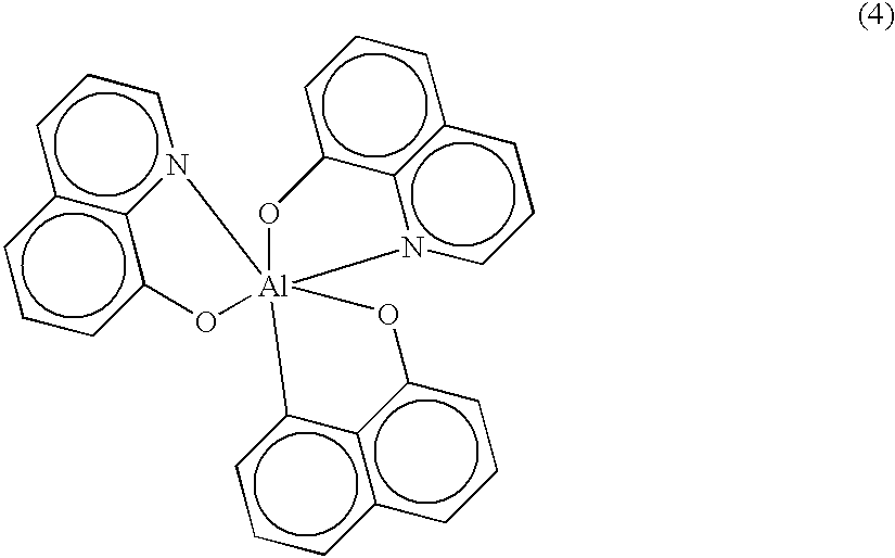
As preferred examples of the nitrogen-containing complexes, mentioned are metal complexes with a ligand of 8-quinolinol derivatives, such as tris (8-quinolinol)Al complex of the following formula (4), as well as tris(5,7-dichloro-8-quinolinol)Al complex, tris(5,7-dibromo-8-quinolinol)Al complex, tris(2-methyl-8-quinolinol)Al complex, tris(5-methyl-8-quinolinol)Al complex, tris (8-quinolinol) Zn complex, tris(8-quinolinol)In complex, tris(8-quinolinol)Mg complex, tris(8-quinolinol)Cu complex, tris(8-quinolinol)Ca complex, tris(8-quinolinol)Sn complex, tris(8-quinolinol)Ga complex, tris(8-quinolinol)Pb complex, etc. One or more of these may be used either singly or as combined.
Figure US06509109-20030121-C00002
Also preferred as the nitrogen-containing complexes are phthalocyanine derivatives, such as metal-free phthalocyanine, Cu phthalocyanine, Li phthalocyanine, Mg phthalocyanine, Pb phthalocyanine, Ti phthalocyanine, Ga phthalocyanine, CuO phthalocyanine, etc. One or more of these may be used either singly or as combined.
As preferred examples of the nitrogen-containing cyclic compounds, mentioned is at least one compound selected from the group consisting of oxadiazole derivatives, thiadiazole derivatives, triazole derivatives, quinoxaline derivatives and quinoline derivatives.
Of those, specific examples of the preferred oxadiazole derivatives are represented by the following formulae (5) and (6); one specific example of the preferred thiadiazole derivatives is by the following formula (7); that of the preferred triazole derivatives is by the following formula (8); that of the preferred quinoxaline derivatives is by the following formula (9); and that of the preferred quinoline derivatives is by the following formula (10).
Figure US06509109-20030121-C00003
In addition, heterocyclic tetracarboxylic acid anhydrides of the following compound such as anthrone derivatives, fluorenylmethane derivatives, carbodiimide, naphthaleneperylene, etc.; as well as electron-transmitting compounds that are exemplified in JP-A-59-194393 as the material for light-emitting layer are also preferably used herein.
Reducing Dopant Having a Work Function of at Most 2.9 eV
The electron injection region in the second embodiment contains a reducing dopant having a work function of at most 2.9 eV. The reducing dopant having a work function of at most 2.9 eV is meant to indicate a substance which has a work function of at most 2.9 eV and which, even when the co-existing, electron-transporting compound is oxidized, can reduce the oxidized electron-transporting compound to a certain degree. Therefore, so far as it has a work function of at most 2.9 eV, the reducing dopant for the first embodiment which may be at least one substance selected from the group consisting of alkali metals, alkaline earth metals, rare earth metals, alkali metal oxides, alkali metal halides, alkaline earth metal oxides, alkaline earth metal halides, rare earth metal oxides and rare earth metal halides is favorably used herein.
More concretely, the preferred reducing dopant having a work function of at most 2.9 eV is at least one alkali metal selected from the group consisting of Na (having a work function of 2.36 eV), K (having a work function of 2.28 eV), Rb (having a work function of 2.16 eV) and Cs (having a work function of 1.95 eV), or at least one alkaline earth metal selected from the group consisting of Ca (having a work function of 2.9 eV), Sr (having a work function of from 2.0 to 2.5 eV) and Ba (having a work function of 2.52).
Of those, the reducing dopant is more preferably at least one alkali metal selected from the group consisting of K, Rb and Cs, even more preferably Rb or Cs, most preferably Cs. These alkali metals have an especially high degree of reducing ability. Therefore, even when a relatively small amount of the reducing dopant selected from them is in the electron injection region, the luminance of the organic EL device is much increased and the lifetime thereof is much prolonged.
As the reducing dopant having a work function of at most 2.9 eV, a combination of two or more of those alkali metals is also preferred. Especially preferred is a combination comprising Cs and one or two others. For example, the combination includes Cs and Na; Cs and K; Cs and Rb; and Cs, Na and K. Those combinations comprising Cs could exhibit much increased reducing ability. Therefore, with any of those combinations being in the electron injection region, the luminance of the organic EL device is still more increased and the lifetime thereof is still more prolonged.
The amount of the reducing dopant having a work function of at most 2.9 eV, which is to be in the electron injection region, is described. Like that in the first embodiment, the amount of the reducing dopant to be in the electron injection region in the second embodiment preferably falls between 0.1 and 50% by weight, more preferably between 1 and 20% by weight, relative to the sum total of the components constituting the region of being 100% by weight.
Regarding the amount of the reducing dopant having a work function of at most 2.9 eV that is to be in the electron injection region, it is desirable that the ratio of the electron-transporting compound to the reducing dopant falls between 1:20 and 20:1 (by mol). If the ratio of the electron-transporting compound to the reducing dopant falls outside the defined range, the luminance of the organic EL device will be lowered and the lifetime thereof will be shortened.
Accordingly, it is more desirable that the ratio of the electron-transporting compound to the reducing dopant falls between 1:10 and 10:1 (by mol), even more preferably between 1:5 and 5:1, most preferably between 1:3 and 3:1.
Electron Affinity
Like in the first embodiment, it is desirable that the electron affinity of the electron injection region in the second embodiment falls between 1.8 and 3.6 eV, more preferably between 1.9 and 3.0 eV, even more preferably between 2.0 and 2.5 eV. If the electron affinity oversteps the defined range, undesired complexes with low luminous efficiency will be readily formed and, in addition, it will be difficult to prevent the blocking contact from being formed at the interface between electron injection region and the light emission region.
The electron affinity of the electron injection region could be suitably controlled by changing the types of the electron-transporting compound and the reducing dopant that constitute the region and by changing the ratio of the two.
Also as in the first embodiment, it is still more desirable that the difference in the electron affinity between the electron injection region and the light emission region in the second embodiment is at most 0.5 eV, even more preferably at most 0.2 eV. In the organic EL device in which the electron affinity difference between the two regions is smaller, the electron transfer from the electron injection region to the light emission region is easier. With that constitution, therefore, the device ensures fast response.
Glass Transition Point
Like in the first embodiment, it is desirable that the glass transition point of the electron injection region in the second embodiment is 100° C. or higher, but more preferably falling between 105 and 200° C.
Third Embodiment
With reference to FIG. 2, the third embodiment of the invention is described. FIG. 2 is a cross-sectional view of an organic EL device 102 of the third embodiment, which comprises an anode layer 10, a hole injection and transportation layer 18, a light emission region 12, an electron injection region 14 and a cathode layer 16 as laminated in that order.
The organic EL device 102 is the same as the organic EL device 100 of the first and second embodiments, except that, in the former, the hole injection and transportation layer 18 is between the anode layer 10 and the light emission region 12.
Accordingly, the characteristic part of the hole injection and transportation layer 18 in the third embodiment is described in detail hereinunder, while the other parts, such as the electron injection region 14 and others could be the same as or similar to those in the first or second embodiment.
The hole injection and transportation layer 18 in the third embodiment has the function of smoothly receiving holes from the anode layer, substantially like an ordinary hole injection layer, and has an additional function of efficiently transporting the holes to the light emission region. Therefore, the hole injection and transportation layer 18 facilitates the injection and transportation of holes to the light emission region, thereby ensuring fast responsibility of the organic EL device.
The hole injection and transportation layer 18 is made of an organic or inorganic material. Preferred examples of the organic material are diamine compounds, diamine-containing oligomers and thiophene-containing oligomers. Preferred examples of the inorganic material are amorphous silicon (α-Si), α-SiC, microcrystalline silicon (μC-Si), μC-SiC, compounds of II-VI Groups, compounds of III-V Groups, amorphous carbon, crystalline carbon and diamond.
The structure of the hole injection and transportation layer 18 is not limited to only a single-layered one. For example, it may have any of a two-layered structure or a three-layered structure.
The thickness of the hole injection and transportation layer 18 is not also specifically defined. Preferably, however, it falls between 0.5 nm and 5 μm.
Fourth Embodiment
With reference to FIG. 3, the fourth embodiment of the invention is described. FIG. 3 is a cross-sectional view of an organic EL device 104 of the fourth embodiment, which comprises an anode layer 10, a hole injection and transportation layer 18, a light emission region 12, an electron injection region 14, a first interlayer 20 and a cathode layer 16 as laminated in that order.
The organic EL device 104 is the same as the organic EL device 102 of the third embodiment, except that, in the former, the first interlayer 20 is between electron injection region 14 and the cathode layer 16.
Accordingly, the characteristic part of the first interlayer 20 in the fourth embodiment is described in detail hereinunder. The other parts could be the same as or similar to those in the first to third embodiments, or for those, ordinary structures known in the art of organic EL devices shall apply thereto.
The first interlayer 20 in the fourth embodiment has the function of enhancing the electron injection into the light emission region. Therefore, the first interlayer 20 facilitates the injection and transportation of electrons to the light emission region, thereby ensuring fast responsibility of the organic EL device.
The first interlayer 20 is made of a material with electron injection capabilities. Preferred examples of the material are alkali metal compounds, alkaline earth metal compounds, alkali metal-containing amorphous substances, and alkali metal-containing microcrystalline substances.
More concretely, the alkali metal compounds include, for example, LiF, Li2O, LiO and LiCl. Preferred examples of the alkaline earth metal compounds are BaO, SrO, MgO, MgF2 and SrCl2.
The structure of the first interlayer is not limited to only a single-layered one. For example, it may have any of a two-layered structure or a three-layered structure. The thickness of the first interlayer is not also specifically defined. Preferably, however, it falls between 0.1 nm and 10 μm.
Fifth Embodiment
With reference to FIG. 4, the fifth embodiment of the invention is described. FIG. 4 is a cross-sectional view of an organic EL device 106 of the fifth embodiment, which comprises an anode layer 10, a second interlayer 24, a hole injection and transportation layer 18, a light emission region 12, an electron injection region 14 and a cathode layer 16 as laminated in that order.
The organic EL device 106 is the same as the organic EL device 102 of the third embodiment, except that, in the former, the second interlayer 24 is between the anode layer 10 and the hole injection and transportation layer 18. Accordingly, the characteristic part of the second interlayer 24 as provided between the anode layer 10 and the hole injection and transportation layer 18 in the fifth embodiment is described in detail hereinunder. The other parts could be the same as or similar to those in the first to fourth embodiments, or for those, ordinary structures known in the art of organic EL devices shall apply thereto.
The second interlayer 24 in the fifth embodiment has the function of enhancing the hole injection from the anode layer 10 into the light emission region. Therefore, the second interlayer 24 facilitates the injection and transportation of holes to the light emission region, thereby ensuring fast responsibility of the organic EL device.
As the material constituting the second interlayer, employable are any of polyaniline, amorphous carbon and phthalocyanines. The structure of the second interlayer is not limited to only a single-layered one. For example, it may have any of a two-layered structure or a three-layered structure. The thickness of the second interlayer is not also specifically defined. Preferably, however, it falls between 0.5 nm and 5 μm.
Sixth Embodiment
With reference to FIG. 7 to FIG. 9, the sixth embodiment of the invention is described. The sixth embodiment is to provide a method for fabricating organic EL devices, in which the compositional ratio of the materials constituting the electron injection region and others could be unified, even though the region and others have a large area, thereby reducing the fluctuation in the driving voltage for the devices and prolonging the lifetime of the devices. Another advantage of the method is that the space for the devices to be fabricated therein could be reduced.
Specifically, the method is for vapor deposition for forming thin films for organic EL devices. As one example, for this, used is a vaccum evaporation apparatus 201 as in FIG. 7 and FIG. 8. In the apparatus 201, different materials for deposition are vaporized all at a time from a plurality of vapor sources as put in their containers 212A to 212F that are disposed to face the substrate 203 therein. The vapors from those materials are deposited on the substrate 203 to form thin films thereon. Relative to the substrate 203, settled is a rotation axis line 213A around which the substrate 203 rotates on its own axis, and the vapor source containers 212A to 212F are all disposed below the substrate 203 while being spaced from the rotation axis line 213A of the substrate 203. In the apparatus, while the substrate 203 rotates on its own axis around the rotation axis line 213A, the vapors from the sources are deposited thereon.
The vaccum evaporation apparatus 201 of FIG. 7 and FIG. 8 comprises a vacuum chamber 210, a substrate holder 211 as disposed in the upper site of the vacuum chamber 210 to hold the substrate 203 with it, and a plurality of (six herein) vapor source containers 212A to 212F for different vapor sources all disposed below the substrate holder 211 while facing the substrate holder 211. The vacuum chamber 210 is kept in a predetermined vacuum condition by means of a degassing means (not shown). The number of the vapor source containers illustrated is 6, which, however, is not limitative. It may be 5 or less, or may even be 7 or more.
The substrate holder 211 is provided with a holding part 212 that supports the periphery of the substrate 203, and it holds the substrate 203 horizontally in the vacuum chamber 210. A rotary shaft 213 is vertically fitted to the upper surface of the substrate holder 211 at its center, and the substrate 203 rotates on its own axis around the rotary shaft 213. The rotary shaft 213 is connected with a rotational driving means of a motor 214. Owing to the rotational motion of the motor 214, the substrate 203 as held by the substrate holder 211 rotates, along with the substrate holder 211, on its own axis around the rotary shaft 213. Specifically, in this apparatus, the rotation axis line 213A of the rotary shaft 213 is settled in the vertical direction relative to the center of the substrate 203.
Now concretely described is the method for forming a film of the electron injection region 14 on the substrate 203 in the vaccum evaporation apparatus 201 having the constitution noted above
First prepared is the substrate 203 of a flat plate having a square surface, and this is horizontally held by the substrate holder 211 while being clamped by the holding part 212, as in FIG. 7 and FIG. 8. FIG. 8 illustrates this condition, in which the part with hatching indicates the substrate 203 as horizontally held by the substrate holder 211.
To form the film of the electron injection region 14 in the apparatus illustrated, an electron-transporting compound and a reducing dopant are put separately in the two vapor source containers 212B and 212C that are adjacent to each other on the virtual circle 221, and then the vacuum chamber 210 is degassed through a degassing means to a predetermined vacuum degree of, for example, 1.0×10⁻⁴ Pa.
Next, the vapor source containers 212B and 212C are heated so that the electron-transporting compound and the reducing dopant are simultaneously vaporized from the separate containers 212B and 212C, while, on the other hand, the motor 214 is rotationally driven so that the substrate 203 is rotated around the rotation axis line 213A at a predetermined speed of, for example, falling between 1 and 100 rpm. In that manner, while the substrate 203 is made to rotate on its own axis, the electron-transporting compound and the reducing dopant are co-deposited on the substrate to form thereon a film of the electron injection region 14.
In this stage, the vapor source containers 212B and 212C are both spaced from the rotation axis line 213A of the substrate 203 by a predetermined distance M in the horizontal direction, as in FIG. 8. Therefore, owing to the rotation of the substrate 203, the incident angle of the vapor stream of the electron-transporting compound and that of vapor stream of the reducing dopant relative to the substrate 203 could be regularly varied.
Accordingly, the vaporized materials could be uniformly deposited on the substrate 203, and the compositional ratio of the materials is unified in the film of the electron injection region 14 thus formed. For example, in the thin film formed in this method, the concentration unevenness could be surely reduced to ±10% (by mol).
The vapor deposition to be effected according to the method does not require any additional revolution of the substrate 203. Therefore, the space and the equipment for the additional revolution of the substrate 203 are unnecessary, and the filming can be economically attained in a minimized space. The additional revolution of the substrate as referred to herein is meant to indicate that the substrate is additionally rotated, except for its rotation on its own axis, around any other rotation axes. For this, needed is a broader space than that needed for the case illustrated herein where the substrate is made to rotate on its own axis only.
In the method of the sixth embodiment, the shape of the substrate 203 is not specifically defined. However, it is desirable that the substrate 203 is of a rectangular tabular shape, for example, as in FIG. 7 and FIG. 8. In the illustrated case, it is also desirable that a plurality of vapor source containers 212A to 212E are disposed along the circumference of the virtual circle 221 as drawn around the rotation axis line 213A of the substrate 203 as its center so as to satisfy the condition of M>½×L where M indicates the radius of the virtual circle 221 and L indicates the length of one side of the substrate 203. Where all the sides of the substrate 203 are not the same but differ, L shall indicates the longest side thereof.
With that constitution, the incident angles of the vapor streams of different vaporizing materials running out of the plural vapor source containers 212A to 212E toward the substrate 203 could be all the same relative to the substrate 203, and therefore, the compositional ratio of the materials deposited on the substrate 203 is more easy to control.
With that constitution, in addition, the materials are vaporized and run toward the substrate 203 at a predetermined incident angle relative to the substrate 203, but not vertically thereto. Therefore, the uniformity of the compositional ratio in the film deposited on the substrate 203 could be much more increased.
In the method of the sixth embodiment, where a plurality of vapor source containers 212A to 212E are disposed on the circumference of the virtual circle 221 as drawn around the rotation axis line 213A of the substrate 203 as its center, as in FIG. 7, and where a mixture phase zone of two or more materials (e.g., the electron-transporting compound and the reducing dopant as in the case illustrated herein) is intended to be formed in a uniform compositional ratio, it is desirable that the vapor source-containers for those materials are positioned to be adjacent to each other. As opposed to this, however, where the compositional ratio of the materials deposited on the substrate is intended to vary in the direction of the thickness of the deposited film, it is desirable that the vapor source containers for those materials are positioned to be remote from each other. For example, when the number of the vapor sources is represented by “n”, the vapor source containers may be disposed at an angle of 360°/n to each other relative to the center of the circle.
The uniformity of the thin film layers to be formed according to the method of the sixth embodiment is described in detail. In one example, Alq was used as the electron-transporting compound and Cs was as the reducing dopant, and a glass substrate 203 shown in FIG. 9 was coated with a thin film layer of those substances having a thickness of about 1000 Å (defined value), while being rotated at 5 rpm. For this, the two substances were vaporized simultaneously for co-deposition, under the condition mentioned below.
Deposition rate of Alq: 0.2 nm/sec.
Deposition rate of Cs: 0.03 nm/sec.
Thickness of Alq/Cs: 1000 Å (defined value).
Using a profilometer, the thickness of the thus-formed thin film was measured at different points (4 A to 4 M) on the glass substrate 203, as in FIG. 9. In addition, the compositional ratio of Cs/Al in the film was measured through electron spectroscopy for chemical analysis (ESCA) using an X-ray photoelectron spectrometer. In FIG. 9, the points for measurement (4 A to 4 M) on the glass substrate 203 were settled as follows: The surface of the substrate 203 was divided into 16 equal square sections, each having one side, P, of being 50 mm long, and any desired corners of those sections were selected for the points (13 in all) .The data obtained are shown in Table 1.
TABLE 1
Point for
Measurement Thickness (Å) Cs/Al (−)
4A 1053 1.0
4B 1035 1.0
4C 1047 1.0
4D 1088 1.1
4E 1091 1.0
4F 1093 1.1
4G 1082 1.1
4H 1075 1.0
4I 1082 1.1
4J 1065 1.1
4K 1010 1.0
4L 1008 1.0
4M 1025 1.0
In another example, a thin film having a thickness of about 1000 Å (defined value) was formed in the same manner as above for the method of the sixth embodiment. In this, however, the substrate 203 was not rotated. The condition for deposition was the same as above. The thickness of the thin film formed and the compositional ratio of Cs/Al in the film were measured at different points (4 A to 4 M), in the same manner as above. The data obtained are shown in Table 2.
TABLE 2
Point for
Measurement Thickness (Å) Cs/Al (−)
4A 895 0.6
4B 941 1.1
4C 884 1.1
4D 911 0.7
4E 922 1.1
4F 1022 0.8
4G 919 1.2
4H 1015 1.3
4I 1067 0.7
4J 908 1.2
4K 895 0.5
4L 920 1.0
4M 950 1.1
As is obvious from those data, it is known that the thin film as formed according to the method of the sixth embodiment is highly uniform in its thickness that falls within the scope between 1008 and 1091 Å at all points (4 A to 4 M) on the substrate 203 and in its compositional ratio of Cs/Al (by mol) that falls within the scope between 1.0 and 1.10 (−) at those points.
Contrary to this, it is known that the thin film as formed according to the method which differs from the method of the sixth embodiment is not uniform in its thickness that varies in a wide scope between 884 and 1067 Å at the points (4 A to 4 M) on the substrate 203 and in its compositional ratio of Cs/Al (by mol) that varies also in a wide scope between 0.6 and 1.2 (−) at those points.
Some specific embodiments of the invention have been described hereinabove, but these are not intended to restrict the scope of the invention. The embodiments illustrated herein could be modified and changed indifferent manners. For example, in the embodiments, the light emission region and the electron injection region are provided separately, but are not limitative. In the invention, the light emission region and the electron injection region may be combined in one layer, if desired. In addition, any optional layers could be provided between the cathode layer and the anode layer.
The invention is described in more detail with reference to the following Examples, which, needless-to-say, are not intended to restrict the scope of the invention.
EXAMPLE 1
FIG. 5, FIG. 7 and FIG. 8 are referred to for Example 1 of the invention. The structure of the organic EL device 102 a of Example 1 as illustrated in FIG. 5 corresponds to the organic EL device 102 of the third embodiment illustrated in FIG. 2. However, the organic EL device 102 a of Example 1 differs from the organic EL device 102 of the third embodiment in that, in the former, the hole injection and transportation layer 18 is composed of two layers, a hole injection layer 18 a and a hole transportation layer 18 b, as laminated in that order.
(1) Preparation for Fabrication of Organic EL Device
In fabricating the organic EL device 102 a of Example 1, a transparent electrode film of ITO was formed, as the anode layer 10, on a glass substrate 22 having a thickness of 1.1 mm, a length of 200 mm and a width of 200 mm. A combination of the glass substrate 22 and the anode layer 10 is referred to as a substrate 30 (this is designated as 203 in FIG. 7 and FIG. 8). Next, the substrate 30 was ultrasonically cleaned with isopropyl alcohol, then dried in an N2 (nitrogen gas) atmosphere, and thereafter washed with UV (ultraviolet rays) and ozone for 10 minutes.
Next, the substrate 30 was fitted to the substrate holder 211 in the vacuum chamber 210 of the vaccum evaporation apparatus 201, as in FIG. 8; while a hole-injecting organic substance (HI-1) for forming the hole injection layer 18 a was put in the vapor source container 212A, a hole-injecting and transporting organic substance (HT-1) for forming the hole transportation layer 18 b was in the vapor source container 212B, a nitrogen-free aromatic compound (EM-1) for forming the electron injection region and the light emission region was in the vapor source container 212C, a reducing dopant (Li) for forming the electron injection region was in the vapor source container 212D, and a metal (Al) for forming the cathode layer was in the vapor source container 212E.
HI-1 is represented by the following structural formula (11); HT-1 is by the following structural formula (12); and EM-1 is by the following structural formula (13). EM has a glass transition point of 105° C., and the electron affinity of the electron injection region containing it was 2.8 eV.
Figure US06509109-20030121-C00004
(2) Fabrication of organic EL device
Next, the vacuum chamber 210 was degassed to a vacuum degree of 5×10⁻⁵ Pa or lower. In that condition, the hole injection layer 18 a, the hole transportation layer 18 b, the light emission region 12, the electron injection region 14 and the cathode layer 16 were deposited in that order on the anode layer 10 of the substrate 30 to fabricate the organic EL device 102 a. Throughout the process from the formation of the hole injection layer 18 a to the formation of the cathode layer 16, the vacuum condition in the chamber was not broken at all, and the organic EL device 102 a was thus fabricated in the continuous vacuum condition.
More concretely, HI-1 in the vapor source container 212A was vaporized and deposited on the anode layer 10 to form thereon the hole injection layer 18 a; and then, HT-1 in the vapor source container 212B was vaporized and deposited on the hole injection layer 18 a to form thereon the hole transportation layer 18 b. The deposition condition is shown below. During the deposition, the substrate 30 was neither heated nor cooled.
Deposition rate of HI-1: 0.1 to 0.3 nm/sec.
Thickness of HI-1 film: 60 nm.
Deposition rate of HT-1: 0.1 to 0.3 nm/sec.
Thickness of HT-1 film: 20 nm.
Next, the organic light-emitting material, EM-1 in the vapor source container 212C was vaporized and deposited on the hole transportation layer 18 b to form thereon the organic light emission region 12, in the same manner as in the formation of the hole injection layer 18 a. The deposition condition for it is as follows:
Deposition rate of EM-1: 0.1 to 0.3 nm/sec.
Thickness of EM-1 film: 40 nm.
Next, EM-1 and Li in the vapor source containers 212C and 212D, respectively, were simultaneously vaporized and deposited on the organic light emission region 12 to form thereon the electron injection region 14, for which the deposition condition is as follows:
Deposition rate of EM-1: 0.1 to 0.3 nm/sec.
Deposition rate of Li: 0.05 to 0.01 nm/sec.
Thickness of EM-1/Li film: 20 nm.
For the co-deposition, herein employed was the method of the sixth embodiment. Precisely, the vapor source containers 212C and 212D were spaced from the rotation axis line 213A of the substrate 30 (203) by 30 mm in the horizontal direction. In that condition, the vapor source containers 212C and 212D were heated so that EM-1 and Li in those were simultaneously vaporized, while the substrate 203 was made to rotate on its own axis at 5 rpm around the rotation axis line 213A, by rotationally driving the motor 214, thereby forming a film of the electron injection region 14.
Finally, Al in the vapor source container 212E was vaporized and deposited on the electron injection region 14 to form thereon the cathode layer 16, for which the deposition condition is as follows:
Deposition rate of Al: 1 nm/sec.
Thickness of Al film: 200 nm.
(3) Evaluation of Organic EL Device
To the organic EL device 102 a thus fabricated, applied was a direct-current voltage of 7 V between the cathode layer 16 of being a minus (−) electrode and the anode layer 10 of being a plus (+) electrode. As shown in Table 3 below, the current density was 1.0 mA/cm2, the luminance was 40 cd/m2, and the emitted light was blue.
The half lifetime of the device 102 a was 1000 hours. The half lifetime as referred to herein is meant to indicate the time taken by the device before its luminance is attenuated to a half of its maximum luminance. For example, for the device of Example 1, its maximum luminance is 40 cd/m2. Therefore, the time taken by the device before its luminance is attenuated to a half of its maximum luminance, 20 cd/m2, indicates the half lifetime of the device. The data of the device obtained herein are shown in Table 3.
TABLE 3
Light Electron Injection Current Electron Half
Emission Region Density Luminance Affinity lifetime
Example Region Material Molar Ratio (mA/cm2) (cd/m2) (eV) (hrs)
1 EM-1 EM-1/Li 1/1 1 40 2.8 1000
2 EM-1 EM-1/Ca 1/1 1.2  50 2.8 1500
3 EM-1 EM-1/Na 1/1 1  60 2.8 1600
4 EM-1 EM-1/K   1/1.3 4 146 2.2 1800
5 EM-1 EM-1/Cs 1/1 40 1000  2.0 2500
6 EM-1 EM-1/Cs   1/1.5 38 1300  2.0 3000
7 EM-1 EM-1/Cs   1/4.0 25 1100  2.0 1700
8 EM-1 EM-1/Cs/Na 1/1/0.5 40 1000  2.0 2500
9 EM-1 DFAD/Li 1/1 1.5  60 2.8 1800
10 EM-1 Alq/Cs 1/1 25 500 2.0 2500
11 Alq Alq/Na 2/1 3 200 2.3 3000
12 EM-1 H1/CS 1/1 5 700 2.5 1000
13 EM-1 H2/Sr 1/1 1.5 200 2.6 2000
EXAMPLE 2
Example 2 of the invention is described. The structure of the organic EL device of Example 2 is the same as that of the organic EL device 102 a of Example 1, and was fabricated in the same manner as in Example 1. In Example 2, however, a metal of Ca (calcium) was used as the reducing dopant to be in the electron injection region, in place of the Li metal in Example 1.
As in Example 1, a direct-current voltage of 7 V was applied to the organic EL device fabricated herein. As shown in Table 3 above, the current density of the device of Example 2 was 1.2 mA/cm2, the luminance thereof was 50 cd/m2, and the half lifetime thereof was 1500 hours. The data obtained are all in Table 3.
EXAMPLE 3
Example 3 of the invention is described. The structure of the organic EL device of Example 3 is the same as that of the organic EL device 102 a of Example 1, and was fabricated in the same manner as in Example 1. In Example 3, however, a metal of Na (sodium) was used as the reducing dopant to be in the electron injection region, in place of the Li metal in Example 1.
As in Example 1, a direct-current voltage of 7 V was applied to the organic EL device fabricated herein. As shown in Table 3 above, the current density of the device of Example 3 was 1.0 mA/cm2, the luminance thereof was 60 cd/m2, and the half lifetime thereof was 1600 hours. The data obtained are all in Table 3.
EXAMPLE 4
Example 4 of the invention is described. The structure of the organic EL device of Example 4 is the same as that of the organic EL device 102 a of Example 1, and was fabricated in the same manner as in Example 1. In Example 4, however, a metal of K (potassium) was used in an amount of 1.3 mols relative to one mol of EM-1, as the reducing dopant to be in the electron injection region, in place of the Li metal in Example 1.
As in Example 1, a direct-current voltage of 7 V was applied to the organic EL device fabricated herein. As shown in Table 3 above, the current density of the device of Example 4 was 4.0 mA/cm2, the luminance thereof was 146 cd/m2, and the half lifetime thereof was 1800 hours. The data obtained are all in Table 3.
EXAMPLES 5 to 7
Examples 5 to 7 of the invention are described. The structure of the organic EL devices of Examples 5 to 7 is the same as that of the organic EL device 102 a of Example 1, and were fabricated in the same manner as in Example 1. In Examples 5 to 7, however, a metal of Cs (cesium) was used in an amount of 1 mol (Example 5), 1.5 mols (Example 6) and 4.0 mols (Example 7) relative to one mol of EM-1, as the reducing dopant to be in the electron injection region, in place of the Li metal in Example 1.
As in Example 1, a direct-current voltage of 7 V was applied to each organic EL device fabricated herein. The current density was 40 mA/cm2 in Example 5, 38 mA/cm2 in Example 6 and 25 mA/cm2 in Example 7. The data obtained herein will mean that the devices having a smaller amount of Cs added thereto could produce a relatively higher current density in some degree.
The luminance of the devices was 1000 cd/m2 in Example 5, 1300 cd/m2 in Example 6, and 1100 cd/m2 in Example 7.
The half lifetime of the devices was 2500 hours in Example 5, 3000 hours in Example 6, and 1700 hours in Example 7.
EXAMPLE 8
Example 8 of the invention is described. The structure of the organic EL device of Example 8 is the same as that of the organic EL device 102 a of Example 1, and was fabricated in the same manner as in Example 1. In Example 8, however, a mixture of Cs and Na (1.0 mol of Cs and 0.5 mols of Na, relative to 1 mol of EM-1) was used as the reducing dopant to be in the electron injection region, in place of the Li metal in Example 1.
As in Example 1, a direct-current voltage of 7 V was applied to the organic EL device fabricated herein. The current density of the device of Example 9 was 4.0 mA/cm2, the luminance thereof was 1000 cd/m2, and the half lifetime thereof was 2500 hours. The data obtained are all in Table 3.
EXAMPLE 9
Example 9 of the invention is described. The structure of the organic EL device of Example 9 is the same as that of the organic EL device of Example 1. In Example 9, however, diphenylanthracene dimer (DFAD) of the following formula (14) was used as the material for the electron injection region, in place of EM-1 in Example 1. The glass transition point of the electron injection region in this Example was measured through DSC, and was 120° C. In this Example, the other layers except the electron injection region were all the same in their materials and thickness as in Example 1.
Figure US06509109-20030121-C00005
As in Example 1, a direct-current voltage of 7 V was applied to the organic EL device fabricated herein. The current density of the device of Example 9 was 1.5 mA/cm2, the luminance thereof was 60 cd/m2, and the half lifetime thereof was 1800 hours. The data obtained are all in Table 3.
EXAMPLE 10
Example 10 of the invention is described. The structure of the organic EL device of Example 10 is the same as that of the organic EL device of Example 1. In Example 10, however, Alq of formula (4) was used as the material for the electron injection region, in place of EM-1, a metal of Cs (cesium) was used as the reducing dopant in place of Li, and the ratio of Cs to Alq was 1/1 (by mol) . The glass transition point of the electron injection region in this Example was measured through DSC, and was 180° C. In this Example, the other layers except the electron injection region were all the same in their materials and thickness as in Example 1.
As in Example 1, a direct-current voltage of 7 V was applied to the organic EL device fabricated herein. The current density of the device of Example 10 was 25 mA/cm2, the luminance thereof was 500 cd/m2, and the half lifetime thereof was 2500 hours. The data obtained are all in Table 3.
EXAMPLE 11
Example 11 of the invention is described. The structure of the organic EL device of Example 11 is the same as that of the organic EL device of Example 1. In Example 11, however, Alq of formula (4) was used as the material for the electron injection region, in place of EM-1, a metal of Na (sodium) was used as the reducing dopant in place of Li, and the ratio of Na to Alq was 0.5/1 (by mol). In this Example, the other layers except the electron injection region were all the same in their materials and thickness as in Example 1.
As in Example 1, a direct-current voltage of 7 V was applied to the organic EL device fabricated herein. The current density of the device of Example 11 was 3 mA/cm2, the luminance thereof was 200 cd/m2, and the half lifetime thereof was 3000 hours. The data obtained are all in Table 3.
EXAMPLE 12
Example 12 of the invention is described. The structure of the organic EL device of Example 12 is the same as that of the organic EL device of Example 1. In Example 12, however, a quinoxaline compound (H1) of formula (9) was used as the material for the electron injection region, in place of EM-1, a metal of Cs was used as the reducing dopant in place of Li, and the ratio of Cs to H1 was 1/1 (by mol). The glass transition point of the electron injection region in this Example was measured through DSC, and was 103° C. In this Example, the other layers except the electron injection region were all the same in their materials and thickness as in Example 1.
As in Example 1, a direct-current voltage of 7 V was applied to the organic EL device fabricated herein. The current density of the device of Example 12 was 5 mA/cm2, the luminance thereof was 700 cd/m2, and the half lifetime thereof was 1000 hours. The data obtained are all in Table 3.
EXAMPLE 13
Example 13 of the invention is described. The structure of the organic EL device of Example 13 is the same as that of the organic EL device of Example 1. In Example 13, however, an oxadiazole compound (H2) of the following formula (15) was used as the material for the electron injection region, in place of EM-1, a metal of Sr was used as the reducing dopant in place of Li, and the ratio of Sr to H2 was 1/1 (by mol). The glass transition point of the electron injection region in this Example was measured through DSC, and was 101° C. In this Example, the other layers except the electron injection region were all the same in their materials and thickness as in Example 1.
Figure US06509109-20030121-C00006
As in Example 1, a direct-current voltage of 7 V was applied to the organic EL device fabricated herein. The current density of the device of Example 13 was 1.5 mA/cm2, the luminance thereof was 200 cd/m2, and the half lifetime thereof was 2000 hours. The data obtained are all in Table 3.
EXAMPLE 14
FIG. 6 is referred to for Example 14. The structure of the organic EL device of Example 14 is nearly the same as that of the organic EL device 104 of the fourth embodiment. In Example 14, however, the first interlayer 20 is a BaO (barium oxide) layer having a thickness of 5 nm, which was formed through vaccum evaporation at a deposition rate of 0.1 nm/sec. The other layers except the first interlayer 20 were all the same in their materials and thickness as in Example 1.
As in Example 1, a direct-current voltage of 7 V was applied to the organic EL device fabricated herein. The current density of the device of Example 14 was 2.0 mA/cm2, the luminance thereof was 140 cd/m2, and the half lifetime thereof was 2500 hours. The data obtained are all in Table 4 below.
It is known that the current density, the luminance and the half lifetime of the device of Example 14, as having the first interlayer 20, are all over those of the device of Example 1 not having it.
TABLE 4
Example Example Example Example
14 15 16 1
Light Emission EM-1 EM-1 EM-1 EM-1
Region
Electron Injection EM-1/Li EM-1/Li EM-1/Li EM-1/Li
Region (components)
Electron Injection 1/1 1/1 1/1 1/1
Region (molar ratio
of components)
Interlayer BaO LiF SrO None
Current Density 2.0 2.2 2.0 1.0
(mA/cm2)
Luminance (cd/m2) 140 150 100 40
Electron Affinity 2.8 2.8 2.8 2.8
(eV)
Half lifetime (hrs) 2500 3000 2000 1000
EXAMPLE 15
Example 15 of the invention is described. The structure of the organic EL device of Example 15 is the same as that of the device of Example 14. In Example 15, however, a LiF (lithium fluoride) layer having a thickness of 5 nm was formed through vaccum evaporation as the first interlayer, in place of the BaO layer. In this, the other layers except the first interlayer 20 were all the same in their materials and thickness as in Example 1.
As in Example 1, a direct-current voltage of 7 V was applied to the organic EL device fabricated herein. The current density of the device of Example 15 was 2.2 mA/cm2, the luminance thereof was 150 cd/m2, and the half lifetime thereof was 3000 hours. The data obtained are all in Table 4.
EXAMPLE 16
Example 16 of the invention is described. The structure of the organic EL device of Example 16 is the same as that of the device of Example 14. In Example 16, however, a SrO (strontium oxide) layer having a thickness of 5 nm was formed through vaccum evaporation as the first interlayer, in place of the BaO layer. In this, the other layers except the first interlayer 20 were all the same in their materials and thickness as in Example 1.
As in Example 1, a direct-current voltage of 7 V was applied to the organic EL device fabricated herein. The current density of the device of Example 16 was 2.0 mA/cm2, the luminance thereof was 100 cd/m2, and the half lifetime thereof was 2000 hours. The data obtained are all in Table 4.
Comparative Example 1
Comparative Example 1 is described. The structure of the organic EL device of Comparative Example 1 is the same as that of the device of Example 1. In Comparative Example 1, however, trinitrofluorenone (TNF) of the following formula (16) was used as the material for the electron injection region, in place of “EM-1”. The electron affinity of the electron injection region formed herein was 4.1 eV. In this, the other layers except the electron injection region were all the same in their materials and thickness as in Example 1.
Figure US06509109-20030121-C00007
As in Example 1, a direct-current voltage of 7 V was applied to the organic EL device fabricated herein. The current density of the device was 0.1 mA/cm2, but the luminance thereof could not be detected.
It is believed that, since the electron affinity of the electron injection region of the organic EL device of Comparative Example 1 was 4.1 eV and was high, TNF in the region would have reacted with the component of the light emission region to form some complex, or the excited condition as generated in the light emission region would have transferred to the electron injection region whereby the light emission region would have been inactivated.
Comparative Example 2
Comparative Example 2 is described. The structure of the organic EL device of Comparative Example 2 is the same as that of the device of Example 1. In Comparative Example 2, however, diphenoquinone of the following formula (17) was used as the material for the electron injection region, in place of “EM-1”. The glass transition point of the electron injection region formed herein was 50° C. In this, the other layers except the electron injection region were all the same in their materials and thickness as in Example 1.
Figure US06509109-20030121-C00008
As in Example 1, a direct-current voltage of 7 V was applied to the organic EL device fabricated herein. The current density of the device was 0.2 mA/cm2, and the device gave a luminance of 2 cd/m2 only in an instant, which, however, was immediately extinguished.
It is believed that, in the organic EL device of Comparative Example 2, since the material of the electron injection region contained nitrogen and since the glass transition point of the region was 50° C. and was low, the electron injection region would have been disrupted by the Joule's heat.
Comparative Example 3
Comparative Example 3 is described. The structure of the organic EL device of Comparative Example 3 is the same as that of the device of Example 1. In Comparative Example 3, however, a nitrogen-containing compound of the following formula (18) was used as the material for the electron injection region, in place of “EM-1”. The glass transition point of the electron injection region formed herein was 62° C. In this, the other layers except the electron injection region were all the same in their materials and thickness as in Example 1.
Figure US06509109-20030121-C00009
A direct-current voltage of 6 V was applied to the organic EL device fabricated herein. The current density of the device was 1.0 mA/cm2, and the luminance thereof was 90 cd/m2. However, the half lifetime of the device was only 200 hours. In the pattern of the emission spectrum of the device, seen was a spectral component for red emission.
It is believed that, since the nitrogen-containing compound of formula (18) used in Comparative Example 3 has strong acceptor capabilities, it would have interacted with the component of the light emission region thereby probably resulting in that the device containing the compound in its light emission region would have lost the light emission capabilities. In addition, it is further believed that, since compounds having a molecular weight of not larger than 300 and having a low glass transition point, if used in the electron emission region, would be readily mixed with the component of the light emission region, the compound used herein would have interacted with the component of the light emission region whereby the light emission region would have lost the light emission capabilities.
As has been mentioned in detail hereinabove, the electron injection region in the organic EL device of the first aspect of the invention contains a nitrogen-free aromatic compound and a reducing dopant, and the electron affinity of the electron injection region therein is controlled to fall between 1.8 and 3.6 eV. Accordingly, in the organic EL device of the first aspect, charge-transfer complexes or exciplexes with low luminous efficiency are well prevented from being formed in the interface between the electron injection region and the light emission region, and, in addition, the blocking contact is also well prevented from being formed at the interface between the electron injection region and the light emission region that retards the electron injection from the electron injection region to the light emission region. With those characteristics, therefore, the luminous efficiency of the device is increased and the lifetime thereof is prolonged.
On the other hand, the electron injection region in the organic EL device of the second aspect of the invention contains an electron-transporting compound and a reducing dopant having a work function of at most 2.9 eV, and the electron affinity of the electron injection region therein is controlled to fall between 1.8 and 3.6 eV. Accordingly, in the organic EL device of the second aspect, not only nitrogen-free aromatic compounds but also nitrogen-containing aromatic compounds could be used in the electron injection region. In the device of the second aspect with that constitution, charge-transfer complexes or exciplexes with low luminous efficiency are well prevented from being formed in the interface between the electron injection region and the light emission region, and, in addition, the blocking contact is also well prevented from being formed at the interface between the electron injection region and the light emission region that retards the electron injection from the electron injection region to the light emission region. With those characteristics, therefore, the latitude in selecting the materials for the electron injection region to be in the device of the second aspect is greatly broadened, and, in addition, the luminous efficiency of the device is increased and the lifetime thereof is prolonged.
While the invention has been described in detail and with reference to specific embodiments thereof, it will be apparent to one skilled in the art that various changes and modifications can be made therein without departing from the spirit and scope thereof.

Claims (28)

What is claimed is:
1. An organic electroluminescent device comprising at least an anode layer, a light emission region, an electron injection region and a cathode layer laminated in that order, wherein the electron injection region contains a nitrogen-free aromatic compound and a reducing dopant and the electron affinity of the electron injection region is between 1.8 and 3.6 eV and wherein said electron injection region has a glass transition temperature not lower than 100° C.
2. The organic electroluminescent device as claimed in claim 1, wherein said electron injection region has a glass transition temperature between 105 and 200° C.
3. The organic electroluminescent device as claimed in claim 1, wherein said aromatic compound contains a residue of at least one aromatic ring selected from the group consisting of anthracene, fluorene, perylene, pyrene, phenanthrene, chrysene, tetracene, rubrene, terphenylene, quaterphenylene, sexiphenylene, triphenylene, picene, coronene, diphenylanthracene, benz[a]anthracene and binapthalene.
4. The organic electroluminescent device as claimed in claim 1, wherein said aromatic compound contains a residue of at least one aromatic ring selected from the group consisting of styryl-substituted aromatic rings, distyryl-substituted aromatic rings and tris-styrl-substituted aromatic rings.
5. The organic electroluminescent device as claimed in claim 1, wherein said reducing dopant is at least one substance selected from the group consisting of alkali metals, alkaline earth metals, rare earth metals, alkali metal oxides, alkali metal halides, alkaline earth metal oxides, alkaline earth metal halides, rare earth metal oxides and rare earth metal halides.
6. The organic electroluminescent device as claimed in claim 1, wherein said reducing dopant has a work function of at most 3.0 eV.
7. The organic electroluminescent device as claimed in claim 1, wherein said reducing dopant is at least one alkali metal selected from the group consisting of Li, Na, K, Rb and Cs.
8. The organic electroluminescent device as claimed in claim 1, wherein the energy gap in said electron injection region is at least 2.7 eV.
9. The organic electroluminescent device as claimed in claim 1, wherein the ratio of said aromatic compound to said reducing dopant in said electron injection region falls between 1:20 and 20:1 (by mol).
10. The organic electroluminescent device as claimed in claim 1, wherein both said light emission region and said electron injection region contain the same nitrogen-free aromatic compound.
11. The organic electroluminescent device as claimed in claim 1, which additionally has an interlayer between said cathode layer and said electron injection region and/or between said anode layer and said light emission region.
12. The organic electroluminescent device as claimed in claim 1, wherein said reducing dopant is an alkali metal-coordinated compound of the formula A+Ar6−, wherein A is an alkali metal and Ar is an aromatic compound having from 10 to 40 carbon atoms.
13. The organic electroluminescent device as claimed in claim 1, wherein the amount of said reducing dopant is between 0.01 and 50% by weight, relative to the sum total of the components of said electron injection region.
14. The organic electroluminescent device as claimed in claim 1, wherein the ratio of said aromatic compound to said reducing dopant is 1:20 to 20:1 (by mol).
15. An organic electroluminescent device comprising at least an anode layer, a light emission region, an electron injection region and a cathode layer laminated in that order, wherein the electron injection region contains an electron-transporting compound and a reducing dopant having a work function of at most 2.9 eV, and the electron affinity of the electron injection region is between 1.8 and 3.6 eV,
wherein said electron injection region has a glass transition temperature between 105 and 200° C.
16. An organic electroluminescent device comprising at least an anode layer, a light emission region, an electron injection region and a cathode layer laminated in that order, wherein the electron injection region contains an electron-transporting compound and a reducing dopant having a work function of at most 2.9 eV, and the electron affinity of the electron injection region is between 1.8 and 3.6 eV, wherein said electron injection region has a glass transition temperature not lower than 100° C.
17. The organic electroluminescent device as claimed in claim 16, wherein said reducing dopant is at least one alkali metal or alkaline earth metal selected from the group consisting of Na, K, Rb, Cs, Ca, Sr and Ba.
18. The organic electroluminescent device as claimed in claim 16, wherein both said light emission region and said electron injection region contain the same electron-transporting compound.
19. The organic electroluminescent device as claimed in claim 16, which additionally has an interlayer between said cathode layer and said electron injection region and/or between said anode layer and said light emission region.
20. The organic electroluminescent device as claimed in claim 16, wherein said electron-transporting compound comprises nitrogen-containing heterocyclic compounds.
21. The organic electroluminescent device as claimed in claim 16, wherein said reducing dopant is an alkali metal-coordinated compound of the formula A+Ar6−, wherein A is an alkali metal and Ar is an aromatic compound having from 10 to 40 carbon atoms.
22. The organic electroluminescent device as claimed in claim 16, wherein said nitrogen-containing heterocyclic compounds are at least one selected from the group consisting of nitrogen-containing complexes, quinoline derivatives, quinoxaline derivatives, oxadiazole derivatives, thiadiazole derivatives and triazole derivatives.
23. The organic electroluminescent device as claimed in claim 16, wherein the amount of said reducing dopant is between 0.01 and 50% by weight, relative to the sum total of the components of said electron injection region.
24. The organic electroluminescent device as claimed in claim 16, wherein the ratio of said electron-transporting compound to said reducing dopant in said electron injection region falls between 1:20 and 20:1 (by mol).
25. The organic electroluminescent device as claimed in claim 16, wherein the ratio of said electron transporting compound to the reducing dopant is 1:20 to 20:1 (by mol).
26. The organic electroluminescent device as claimed in claim 16, wherein said electron transporting compound is a nitrogen-containing heterocyclic compound selected from the group consisting of nitrogen-containing complexes and nitrogen-containing cyclic compounds.
27. The organic electroluminescent device as claimed in claim 16, wherein said nitrogen-containing complexes are metal complexes with ligands of 8-quinolinol derivatives.
28. The organic electroluminescent device as claimed in claim 16, wherein said nitrogen-containing cyclic compounds are oxadiazole derivatives, thiadiazole derivatives, quinoxaline derivatives or quinoline derivatives.
US09/281,953 1998-04-08 1999-03-31 Organic electroluminescent device Expired - Lifetime US6509109B1 (en)

Applications Claiming Priority (6)

Application Number Priority Date Filing Date Title
JP10-096220 1998-04-08
JP9622098 1998-04-08
JP10-114123 1998-04-09
JP11412398 1998-04-09
JP25727598A JP3266573B2 (en) 1998-04-08 1998-09-10 Organic electroluminescence device
JP10-257275 1998-09-10

Publications (1)

Publication Number Publication Date
US6509109B1 true US6509109B1 (en) 2003-01-21

Family

ID=27308037

Family Applications (1)

Application Number Title Priority Date Filing Date
US09/281,953 Expired - Lifetime US6509109B1 (en) 1998-04-08 1999-03-31 Organic electroluminescent device

Country Status (6)

Country Link
US (1) US6509109B1 (en)
EP (1) EP0949696A3 (en)
JP (1) JP3266573B2 (en)
KR (1) KR100575987B1 (en)
CN (1) CN1222634C (en)
TW (1) TW417312B (en)

Cited By (62)

* Cited by examiner, † Cited by third party
Publication number Priority date Publication date Assignee Title
US20020086180A1 (en) * 2000-12-28 2002-07-04 Satoshi Seo Luminescent device
US20030173894A1 (en) * 2002-03-15 2003-09-18 Lg.Philips Lcd Co., Ltd. Organic electroluminescent device including transparent conductive layer and fabricating method thereof
US6660411B2 (en) * 2000-09-20 2003-12-09 Mitsubishi Chemical Corporation Organic electroluminescent device
US20040032206A1 (en) * 2002-08-16 2004-02-19 Weaver Michael S. Efficiency transparent cathode
US20040106003A1 (en) * 2002-12-03 2004-06-03 Canon Kabushiki Kaisha Binaphthalene derivatives for organic electro-luminescent devices
US6794061B2 (en) * 2002-01-31 2004-09-21 Eastman Kodak Company Organic electroluminescent device having an adhesion-promoting layer for use with a magnesium cathode
US20050104511A1 (en) * 2003-11-14 2005-05-19 Eastman Kodak Company Organic electroluminescent devices having a stability-enhancing layer
US20050179399A1 (en) * 2004-01-16 2005-08-18 Karl Leo Pixel for an active matrix display
US20050233166A1 (en) * 2004-04-14 2005-10-20 Eastman Kodak Company OLED device using reduced drive voltage
US20050244676A1 (en) * 2000-09-07 2005-11-03 Idemitsu Kosan Co., Ltd. Organic electric-field light-emitting element
US20060006796A1 (en) * 2004-07-09 2006-01-12 Au Optronics Corporation High contrast organic light emitting device
US20060132026A1 (en) * 2004-12-17 2006-06-22 Honeywell International, Inc. Organic light emitting diode (OLED) having improved stability, luminance, and efficiency
US20060147747A1 (en) * 2003-03-13 2006-07-06 Hiroshi Yamamoto Nitrogen-containing heterocycle derivative and organic electroluminescent element using the same
US20060147649A1 (en) * 2005-01-06 2006-07-06 Au Optronics Corp. Photoelectric devices
US20060172147A1 (en) * 2003-07-11 2006-08-03 Masahide Matsuura White organic electroluminescence device
US20060181200A1 (en) * 2005-02-16 2006-08-17 Min-Ling Hung Silane compound, organic electroluminescent device and display panel using the same
US20060204784A1 (en) * 2005-03-10 2006-09-14 Begley William J Organic light-emitting devices with mixed electron transport materials
US20060240278A1 (en) * 2005-04-20 2006-10-26 Eastman Kodak Company OLED device with improved performance
US20060269782A1 (en) * 2005-05-25 2006-11-30 Eastman Kodak Company OLED electron-transporting layer
US20060286405A1 (en) * 2005-06-17 2006-12-21 Eastman Kodak Company Organic element for low voltage electroluminescent devices
US20060286403A1 (en) * 2005-06-20 2006-12-21 Au Optronics Corp. Organic light emitting diode and method of fabricating the same
US20060286402A1 (en) * 2005-06-17 2006-12-21 Eastman Kodak Company Organic element for low voltage electroluminescent devices
US20060292394A1 (en) * 2005-06-22 2006-12-28 Semiconductor Energy Laboratory Co., Ltd. Light emitting device and electronic appliance using the same
US20070048545A1 (en) * 2005-08-31 2007-03-01 Eastman Kodak Company Electron-transporting layer for white OLED device
US20070085474A1 (en) * 2005-10-19 2007-04-19 Eastman Kodak Company OLED device with improved high temperature operation
US20070092755A1 (en) * 2005-10-26 2007-04-26 Eastman Kodak Company Organic element for low voltage electroluminescent devices
US20070092756A1 (en) * 2005-10-26 2007-04-26 Eastman Kodak Company Organic element for low voltage electroluminescent devices
US20070092759A1 (en) * 2005-10-26 2007-04-26 Begley William J Organic element for low voltage electroluminescent devices
US20070092753A1 (en) * 2005-10-26 2007-04-26 Eastman Kodak Company Organic element for low voltage electroluminescent devices
US20070092754A1 (en) * 2005-10-26 2007-04-26 Eastman Kodak Company Organic element for low voltage electroluminescent devices
US20070111024A1 (en) * 2003-07-02 2007-05-17 Fumino Okuda Metal complex compound and organic electroluminescence device containing the same
US20070114921A1 (en) * 2002-01-24 2007-05-24 Semiconductor Energy Laboratory Co., Ltd. Light Emitting Device and Method of Manufacturing the Same
US20070114527A1 (en) * 2003-12-26 2007-05-24 Semiconductor Energy Laboratory Co., Ltd. Light-emitting element
US20070126347A1 (en) * 2005-12-01 2007-06-07 Eastman Kodak Company OLEDS with improved efficiency
US20070190356A1 (en) * 2004-03-17 2007-08-16 Takashi Arakane Material for organic electroluminescent element and organic electroluminescent element employing the same
US20070216292A1 (en) * 2004-12-06 2007-09-20 Satoshi Seo Composite Material Including organic Compound And Inorganic Compound Light-Emitting Element And Light-Emitting Device Using The Composite Compound, And Manufacturing Method Of The Light-Emitting Element
US20070241665A1 (en) * 2006-04-12 2007-10-18 Matsushita Electric Industrial Co., Ltd. Organic electroluminescent element, and manufacturing method thereof, as well as display device and exposure apparatus using the same
US20070290604A1 (en) * 2006-06-16 2007-12-20 Matsushita Electric Industrial Co., Ltd. Organic electroluminescent device and method of producing the same
US20080032123A1 (en) * 2006-08-02 2008-02-07 Spindler Jeffrey P Dual electron-transporting layer for oled device
US7378126B2 (en) 2002-02-22 2008-05-27 Semiconductor Energy Laboratory Co., Ltd. Light-emitting device and method of manufacturing the same, and method of operating manufacturing apparatus
US20080160341A1 (en) * 2005-02-22 2008-07-03 Commissariat A L'energie Atomique Organic Light-Emitting Diode With Doped Layers
US20080176099A1 (en) * 2007-01-18 2008-07-24 Hatwar Tukaram K White oled device with improved functions
US20080217608A1 (en) * 2007-02-21 2008-09-11 Semiconductor Energy Laboratory Co., Ltd. Light-Emitting Element, Light-Emitting Device, Electronic Device and Quinoxaline Derivative
US20080246394A1 (en) * 2007-04-03 2008-10-09 Fujikura Ltd. Organic light-emitting diode element and optical interconnection module
US20090001878A1 (en) * 2007-04-03 2009-01-01 Tsinghua University Organic electroluminescent device
US20090017331A1 (en) * 2007-07-10 2009-01-15 Idemitsu Kosan Co., Ltd. Material for organic electroluminescence device and organic electroluminescence device utilizing the same
US20090110957A1 (en) * 2007-10-26 2009-04-30 Begley William J Oled device with certain fluoranthene host
US20090110956A1 (en) * 2007-10-26 2009-04-30 Begley William J Oled device with electron transport material combination
US20090108734A1 (en) * 2007-10-26 2009-04-30 Begley William J Oled device with certain fluoranthene light-emitting dopants
US20090108735A1 (en) * 2007-10-26 2009-04-30 Begley William J Oled device with fluoranthene electron transport materials
US20090167168A1 (en) * 2007-12-28 2009-07-02 Semiconductor Energy Laboratory Co., Ltd. Light-Emitting Element, Light-Emitting Device and Electronic Device
US20100019671A1 (en) * 2005-10-26 2010-01-28 Eastman Kodak Company Organic element for low voltage electroluminescent devices
US20100117520A1 (en) * 2008-11-12 2010-05-13 Begley William J Oled device with fluoranthene electron injection materials
US20100117519A1 (en) * 2008-11-07 2010-05-13 Begley William J Electroluminescent device containing a flouranthene compound
US20100141122A1 (en) * 2008-12-09 2010-06-10 Begley William J Oled device with cyclobutene electron injection materials
US20100207513A1 (en) * 2009-02-13 2010-08-19 Begley William J Oled with fluoranthene-macrocyclic materials
US20100244677A1 (en) * 2009-03-31 2010-09-30 Begley William J Oled device containing a silyl-fluoranthene derivative
US20110073843A1 (en) * 2006-09-29 2011-03-31 Saes Getters S.P.A. Organic Light Emitting Display and Process for its Manufacturing
US20110248251A1 (en) * 2008-10-28 2011-10-13 Idemitsu Kosan Co., Ltd. Nitrogen-containing heterocyclic derivative and organic electroluminescence element using nitrogen-containing heterocyclic derivative
US8623524B2 (en) 2002-10-09 2014-01-07 Idemitsu Kosan Co., Ltd. Organic electroluminescent device
US9748509B2 (en) 2013-07-10 2017-08-29 Joled Inc. Organic EL element and organic EL display panel
US10170724B2 (en) 2002-03-07 2019-01-01 Semiconductor Energy Laboratory Co., Ltd. Light emitting apparatus and method of fabricating the same

Families Citing this family (41)

* Cited by examiner, † Cited by third party
Publication number Priority date Publication date Assignee Title
JP3825725B2 (en) * 1998-05-19 2006-09-27 三洋電機株式会社 Organic electroluminescence device
JP3370011B2 (en) * 1998-05-19 2003-01-27 三洋電機株式会社 Organic electroluminescence device
KR100274871B1 (en) * 1998-11-12 2000-12-15 김순택 Photoluminescence compound and display device adopting photoluminescence compound as color-developing substance
JP4729154B2 (en) * 1999-09-29 2011-07-20 淳二 城戸 Organic electroluminescent device, organic electroluminescent device group, and method for controlling emission spectrum thereof
JP4094203B2 (en) * 2000-03-30 2008-06-04 出光興産株式会社 Organic electroluminescence device and organic light emitting medium
JP2002289360A (en) * 2001-03-27 2002-10-04 Univ Toyama Organic electric field light emitting device
ITMI20010995A1 (en) * 2001-05-15 2002-11-15 Getters Spa CESIUM DISPENSERS AND PROCESS FOR THEIR USE
KR100404860B1 (en) * 2001-06-27 2003-11-07 주식회사 엘리아테크 organic electroluminescent display panel
KR100478520B1 (en) * 2001-08-13 2005-03-28 삼성에스디아이 주식회사 Blue light-emitting compound and display device adopting light-emitting compound as color-developing substance
JP4584506B2 (en) * 2001-08-28 2010-11-24 パナソニック電工株式会社 Organic electroluminescence device
JP5223163B2 (en) * 2001-09-07 2013-06-26 東レ株式会社 Light emitting element
AU2002339150A1 (en) * 2001-11-08 2003-05-19 Cambridge Display Technology Limited Container with organic light emitting device
KR100474891B1 (en) * 2001-12-20 2005-03-08 엘지전자 주식회사 organic electroluminescent display device
JP3825344B2 (en) 2002-03-15 2006-09-27 富士写真フイルム株式会社 Organic EL element and organic EL display
JP4466064B2 (en) * 2003-02-17 2010-05-26 セイコーエプソン株式会社 Manufacturing method of electro-optical device
US7651787B2 (en) 2003-02-19 2010-01-26 Lg Display Co., Ltd. Organic electroluminescent device
US7026658B2 (en) 2003-03-13 2006-04-11 Samsung Sdi, Co., Ltd. Electrical conductors in an electroluminescent display device
EP1467224A1 (en) * 2003-04-07 2004-10-13 CSEM Centre Suisse d'Electronique et de Microtechnique SA Optical proximity detector
US6703180B1 (en) * 2003-04-16 2004-03-09 Eastman Kodak Company Forming an improved stability emissive layer from a donor element in an OLED device
KR100560778B1 (en) 2003-04-17 2006-03-13 삼성에스디아이 주식회사 Organic electroluminescent display device
JP4624653B2 (en) * 2003-05-20 2011-02-02 出光興産株式会社 Organic electroluminescence element and display device
CN100490206C (en) * 2003-12-25 2009-05-20 华南理工大学 Organic/high molecular light emitting diode
US20050164019A1 (en) * 2004-01-22 2005-07-28 General Electric Company Charge transfer-promoting materials and electronic devices incorporating same
JP2005276583A (en) * 2004-03-24 2005-10-06 Idemitsu Kosan Co Ltd Organic electroluminescent element and indicating device
JP2005317439A (en) 2004-04-30 2005-11-10 Seiko Epson Corp Display panel and display device
ITMI20041736A1 (en) 2004-09-10 2004-12-10 Getters Spa MIXTURES FOR LITHIUM EVAPORATION AND LITHIUM DISPENSERS
US8026510B2 (en) 2004-10-20 2011-09-27 Dai Nippon Printing Co., Ltd. Organic electronic device and method for producing the same
ITMI20042279A1 (en) 2004-11-24 2005-02-24 Getters Spa ALKALINE METAL DISPENSER SYSTEM ABLE TO DELIVER HIGH QUANTITIES OF METALS
JP2006190995A (en) * 2004-12-06 2006-07-20 Semiconductor Energy Lab Co Ltd Composite material comprising organic compound and inorganic compound, light emitting element and light emitting device employing the composite material as well as manufacturing method of the light emitting element
KR100703479B1 (en) * 2005-11-16 2007-04-03 삼성에스디아이 주식회사 The organic light emission diode and method of manufacturing the same and the organic light emission display device including the light emission diode
EP2047535A2 (en) * 2006-07-19 2009-04-15 Philips Intellectual Property & Standards GmbH Highly doped electro-optically active organic diode with short protection layer
WO2008010165A2 (en) * 2006-07-19 2008-01-24 Koninklijke Philips Electronics N.V. Electro-optically active organic diode with short protection
TWI500196B (en) 2007-04-30 2015-09-11 Lg Chemical Ltd Organic light emitting device and method of producing the same
KR100922760B1 (en) * 2008-03-03 2009-10-21 삼성모바일디스플레이주식회사 Organic light emitting device
JP2008219033A (en) * 2008-04-14 2008-09-18 Denso Corp Organic el element
KR100981971B1 (en) * 2009-01-23 2010-09-13 삼성모바일디스플레이주식회사 Blue Organic Light Emitting Device
JP4820902B2 (en) * 2009-11-25 2011-11-24 淳二 城戸 Organic electroluminescent device and method for controlling emission spectrum thereof
JP2011124231A (en) * 2009-12-03 2011-06-23 Novaled Ag Method of forming electrical interconnect in organic optical electronic device, method of manufacturing organic optical electronic device, and organic light-emitting device
EP2355199B1 (en) * 2010-01-29 2017-07-05 Novaled GmbH A method for producing an organic light emitting device
JP2011171279A (en) * 2010-01-25 2011-09-01 Fujifilm Corp Organic electric field light-emitting element
WO2011111438A1 (en) * 2010-03-09 2011-09-15 コニカミノルタホールディングス株式会社 Organic electroluminescent member and method for producing organic electroluminescent element

Citations (4)

* Cited by examiner, † Cited by third party
Publication number Priority date Publication date Assignee Title
US5652067A (en) * 1992-09-10 1997-07-29 Toppan Printing Co., Ltd. Organic electroluminescent device
US5705284A (en) * 1990-03-26 1998-01-06 Idemitsu Kosan Co., Ltd. Thin film electroluminescence device
US6013384A (en) 1997-01-27 2000-01-11 Junji Kido Organic electroluminescent devices
US6203933B1 (en) * 1995-05-17 2001-03-20 Tdk Corporation Organic EL element

Family Cites Families (5)

* Cited by examiner, † Cited by third party
Publication number Priority date Publication date Assignee Title
US4579679A (en) * 1981-05-18 1986-04-01 Chevron Research Company Electroactive polymers
US4522745A (en) * 1982-11-17 1985-06-11 Chevron Research Company Fused 5,6,5-membered heterocyclic electroactive polymers
JPH07268317A (en) * 1994-03-31 1995-10-17 Toray Ind Inc Light-emitting element
JPH08259939A (en) * 1995-03-10 1996-10-08 At & T Corp Electron transport material
JP4486713B2 (en) * 1997-01-27 2010-06-23 淳二 城戸 Organic electroluminescent device

Patent Citations (4)

* Cited by examiner, † Cited by third party
Publication number Priority date Publication date Assignee Title
US5705284A (en) * 1990-03-26 1998-01-06 Idemitsu Kosan Co., Ltd. Thin film electroluminescence device
US5652067A (en) * 1992-09-10 1997-07-29 Toppan Printing Co., Ltd. Organic electroluminescent device
US6203933B1 (en) * 1995-05-17 2001-03-20 Tdk Corporation Organic EL element
US6013384A (en) 1997-01-27 2000-01-11 Junji Kido Organic electroluminescent devices

Cited By (122)

* Cited by examiner, † Cited by third party
Publication number Priority date Publication date Assignee Title
US20050244676A1 (en) * 2000-09-07 2005-11-03 Idemitsu Kosan Co., Ltd. Organic electric-field light-emitting element
US7879465B2 (en) 2000-09-07 2011-02-01 Idemitsu Kosan Co., Ltd. Organic electric-field light-emitting element
US20100308315A1 (en) * 2000-09-07 2010-12-09 Idemitsu Kosan Co., Ltd. Organic electric-field light-emitting element
US8841003B2 (en) * 2000-09-07 2014-09-23 Idemitsu Kosan Co., Ltd. Organic electric-field light-emitting element
US6660411B2 (en) * 2000-09-20 2003-12-09 Mitsubishi Chemical Corporation Organic electroluminescent device
US20020086180A1 (en) * 2000-12-28 2002-07-04 Satoshi Seo Luminescent device
US8310147B2 (en) 2000-12-28 2012-11-13 Semiconductor Energy Laboratory Co., Ltd. Luminescent device
US7572522B2 (en) 2000-12-28 2009-08-11 Semiconductor Energy Laboratory Co., Ltd. Luminescent device
US7579089B2 (en) 2000-12-28 2009-08-25 Semiconductor Energy Laboratory Co., Ltd. Luminescent device
US20050260440A1 (en) * 2000-12-28 2005-11-24 Semiconductor Energy Laboratory Co., Ltd., A Japan Corporation Luminescent device
US9627459B2 (en) 2002-01-24 2017-04-18 Semiconductor Energy Laboratory Co., Ltd. Display device having sealing material
US20070114921A1 (en) * 2002-01-24 2007-05-24 Semiconductor Energy Laboratory Co., Ltd. Light Emitting Device and Method of Manufacturing the Same
US8089066B2 (en) 2002-01-24 2012-01-03 Semiconductor Energy Laboratory Co., Ltd. Light emitting device
US9312323B2 (en) 2002-01-24 2016-04-12 Semiconductor Energy Laboratory Co., Ltd. Light emitting device having insulator between pixel electrodes and auxiliary wiring in contact with the insulator
US20100230664A1 (en) * 2002-01-24 2010-09-16 Semiconductor Energy Laboratory Co., Ltd. Light emitting device and method of manufacturing the same
US8779467B2 (en) 2002-01-24 2014-07-15 Semiconductor Energy Laboratory Co., Ltd. Light emitting device having a terminal portion
US7692186B2 (en) 2002-01-24 2010-04-06 Semiconductor Energy Laboratory Co., Ltd. Light emitting device and method of manufacturing the same
US6794061B2 (en) * 2002-01-31 2004-09-21 Eastman Kodak Company Organic electroluminescent device having an adhesion-promoting layer for use with a magnesium cathode
US7378126B2 (en) 2002-02-22 2008-05-27 Semiconductor Energy Laboratory Co., Ltd. Light-emitting device and method of manufacturing the same, and method of operating manufacturing apparatus
US8536784B2 (en) 2002-02-22 2013-09-17 Semiconductor Energy Laboratory Co., Ltd. Light-emitting device and method of manufacturing the same, and method of operating manufacturing apparatus
US20090001896A1 (en) * 2002-02-22 2009-01-01 Semiconductor Energy Laboratory Co., Ltd. Light-Emitting Device and Method of Manufacturing the Same, and Method of Operating Manufacturing Apparatus
US8138670B2 (en) 2002-02-22 2012-03-20 Semiconductor Energy Laboratory Co., Ltd. Light-emitting device and method of manufacturing the same, and method of operating manufacturing apparatus
US10170724B2 (en) 2002-03-07 2019-01-01 Semiconductor Energy Laboratory Co., Ltd. Light emitting apparatus and method of fabricating the same
US11005062B2 (en) 2002-03-07 2021-05-11 Semiconductor Energy Laboratory Co., Ltd. Light emitting apparatus and method of fabricating the same
US20050275340A1 (en) * 2002-03-15 2005-12-15 Lg Philips Lcd Co., Ltd. Organic electroluminescent device including transparent conductive layer and fabricating method thereof
US6927535B2 (en) * 2002-03-15 2005-08-09 Lg. Philips Lcd Co., Ltd. Organic electroluminescent device including transparent conductive layer and fabricating method thereof
US7494396B2 (en) 2002-03-15 2009-02-24 Lg Display Co., Ltd. Organic electroluminescent device including transparent conductive layer and fabricating method thereof
US20030173894A1 (en) * 2002-03-15 2003-09-18 Lg.Philips Lcd Co., Ltd. Organic electroluminescent device including transparent conductive layer and fabricating method thereof
US20040032206A1 (en) * 2002-08-16 2004-02-19 Weaver Michael S. Efficiency transparent cathode
US7061175B2 (en) * 2002-08-16 2006-06-13 Universal Display Corporation Efficiency transparent cathode
US8623524B2 (en) 2002-10-09 2014-01-07 Idemitsu Kosan Co., Ltd. Organic electroluminescent device
US20040106003A1 (en) * 2002-12-03 2004-06-03 Canon Kabushiki Kaisha Binaphthalene derivatives for organic electro-luminescent devices
US6872475B2 (en) * 2002-12-03 2005-03-29 Canon Kabushiki Kaisha Binaphthalene derivatives for organic electro-luminescent devices
US7851071B2 (en) 2003-03-13 2010-12-14 Idemitsu Kosan Co., Ltd. Nitrogen-containing heterocycle derivative and organic electroluminescent element using the same
US8097349B2 (en) 2003-03-13 2012-01-17 Idemitsu Kosan Co., Ltd. Nitrogen containing heterocycle derivative and organic electroluminescent element using the same
EP2174932A3 (en) * 2003-03-13 2011-09-21 Idemitsu Kosan Co., Ltd. Nitrogen-containing heterocycle derivative and organic electroluminescent element using the same
EP2174933A3 (en) * 2003-03-13 2011-09-21 Idemitsu Kosan Co., Ltd. Nitrogen-containing heterocycle derivative and organic electroluminescent element using the same
US20060147747A1 (en) * 2003-03-13 2006-07-06 Hiroshi Yamamoto Nitrogen-containing heterocycle derivative and organic electroluminescent element using the same
US20100193773A1 (en) * 2003-03-13 2010-08-05 Idemitsu Kosan Co., Ltd, Nitrogen-containing heterocycle derivative and organic electroluminescent element using the same
US20070111024A1 (en) * 2003-07-02 2007-05-17 Fumino Okuda Metal complex compound and organic electroluminescence device containing the same
US20060172147A1 (en) * 2003-07-11 2006-08-03 Masahide Matsuura White organic electroluminescence device
US7745016B2 (en) * 2003-07-11 2010-06-29 Idemitsu Kosan Co., Ltd. White organic electroluminescence device
US7138763B2 (en) 2003-11-14 2006-11-21 Eastman Kodak Company Organic electroluminescent devices having a stability-enhancing layer
US20050104511A1 (en) * 2003-11-14 2005-05-19 Eastman Kodak Company Organic electroluminescent devices having a stability-enhancing layer
US20070114527A1 (en) * 2003-12-26 2007-05-24 Semiconductor Energy Laboratory Co., Ltd. Light-emitting element
US8796670B2 (en) 2003-12-26 2014-08-05 Semiconductor Energy Laboratory Co., Ltd. Light-emitting element
US20110156030A1 (en) * 2003-12-26 2011-06-30 Semiconductor Energy Laboratory Co., Ltd. Light-emitting element
US9570697B2 (en) 2003-12-26 2017-02-14 Semiconductor Energy Laboratory Co., Ltd. Light-emitting element
US10886497B2 (en) 2003-12-26 2021-01-05 Semiconductor Energy Laboratory Co., Ltd. Light-emitting element
US20050179399A1 (en) * 2004-01-16 2005-08-18 Karl Leo Pixel for an active matrix display
US20070190356A1 (en) * 2004-03-17 2007-08-16 Takashi Arakane Material for organic electroluminescent element and organic electroluminescent element employing the same
US7192659B2 (en) 2004-04-14 2007-03-20 Eastman Kodak Company OLED device using reduced drive voltage
US20050233166A1 (en) * 2004-04-14 2005-10-20 Eastman Kodak Company OLED device using reduced drive voltage
US20060006796A1 (en) * 2004-07-09 2006-01-12 Au Optronics Corporation High contrast organic light emitting device
US7365486B2 (en) * 2004-07-09 2008-04-29 Au Optronics Corporation High contrast organic light emitting device with electron transport layer including fullerenes
US20130277652A1 (en) * 2004-12-06 2013-10-24 Semiconductor Energy Laboratory Co., Ltd. Composite Material Including Organic Compound and Inorganic Compound, Light-Emitting Element and Light-Emitting Device Using the Composite Compound, and Manufacturing Method of the Light-Emitting Element
US20070216292A1 (en) * 2004-12-06 2007-09-20 Satoshi Seo Composite Material Including organic Compound And Inorganic Compound Light-Emitting Element And Light-Emitting Device Using The Composite Compound, And Manufacturing Method Of The Light-Emitting Element
US7759856B2 (en) * 2004-12-17 2010-07-20 Honeywell International Inc. Organic light emitting diode (OLED) having improved stability, luminance, and efficiency
US20060132026A1 (en) * 2004-12-17 2006-06-22 Honeywell International, Inc. Organic light emitting diode (OLED) having improved stability, luminance, and efficiency
US20060147649A1 (en) * 2005-01-06 2006-07-06 Au Optronics Corp. Photoelectric devices
US20060181200A1 (en) * 2005-02-16 2006-08-17 Min-Ling Hung Silane compound, organic electroluminescent device and display panel using the same
US20080160341A1 (en) * 2005-02-22 2008-07-03 Commissariat A L'energie Atomique Organic Light-Emitting Diode With Doped Layers
US9496499B2 (en) * 2005-02-22 2016-11-15 Commissariat A L'energie Atomique Organic light-emitting diode with doped layers
US20060204784A1 (en) * 2005-03-10 2006-09-14 Begley William J Organic light-emitting devices with mixed electron transport materials
US8057916B2 (en) 2005-04-20 2011-11-15 Global Oled Technology, Llc. OLED device with improved performance
US20060240278A1 (en) * 2005-04-20 2006-10-26 Eastman Kodak Company OLED device with improved performance
US20060269782A1 (en) * 2005-05-25 2006-11-30 Eastman Kodak Company OLED electron-transporting layer
US20060286402A1 (en) * 2005-06-17 2006-12-21 Eastman Kodak Company Organic element for low voltage electroluminescent devices
US20060286405A1 (en) * 2005-06-17 2006-12-21 Eastman Kodak Company Organic element for low voltage electroluminescent devices
US20060286403A1 (en) * 2005-06-20 2006-12-21 Au Optronics Corp. Organic light emitting diode and method of fabricating the same
US8252434B2 (en) 2005-06-22 2012-08-28 Semiconductor Energy Laboratory Co., Ltd. Light emitting device and electronic appliance using the same
US20060292394A1 (en) * 2005-06-22 2006-12-28 Semiconductor Energy Laboratory Co., Ltd. Light emitting device and electronic appliance using the same
US8541114B2 (en) 2005-06-22 2013-09-24 Semiconductor Energy Laboratory Co., Ltd. Light emitting device and electronic appliance using the same
US8017252B2 (en) 2005-06-22 2011-09-13 Semiconductor Energy Laboratory Co., Ltd. Light emitting device and electronic appliance using the same
US8815419B2 (en) 2005-06-22 2014-08-26 Semiconductor Energy Laboratory Co., Ltd. Light emitting device and electronic appliance using the same
US20070048545A1 (en) * 2005-08-31 2007-03-01 Eastman Kodak Company Electron-transporting layer for white OLED device
US7645524B2 (en) 2005-10-19 2010-01-12 Eastman Kodak Company OLED device with improved high temperature operation
US20070085474A1 (en) * 2005-10-19 2007-04-19 Eastman Kodak Company OLED device with improved high temperature operation
US20100019671A1 (en) * 2005-10-26 2010-01-28 Eastman Kodak Company Organic element for low voltage electroluminescent devices
US20070092753A1 (en) * 2005-10-26 2007-04-26 Eastman Kodak Company Organic element for low voltage electroluminescent devices
US20070092755A1 (en) * 2005-10-26 2007-04-26 Eastman Kodak Company Organic element for low voltage electroluminescent devices
KR101271729B1 (en) * 2005-10-26 2013-06-04 글로벌 오엘이디 테크놀러지 엘엘씨 Organic element for low voltage electroluminescent devices
US8956738B2 (en) 2005-10-26 2015-02-17 Global Oled Technology Llc Organic element for low voltage electroluminescent devices
US7767317B2 (en) 2005-10-26 2010-08-03 Global Oled Technology Llc Organic element for low voltage electroluminescent devices
US20070092756A1 (en) * 2005-10-26 2007-04-26 Eastman Kodak Company Organic element for low voltage electroluminescent devices
US20070092754A1 (en) * 2005-10-26 2007-04-26 Eastman Kodak Company Organic element for low voltage electroluminescent devices
US20070207347A1 (en) * 2005-10-26 2007-09-06 Eastman Kodak Company Organic element for low voltage electroluminescent devices
US20070092759A1 (en) * 2005-10-26 2007-04-26 Begley William J Organic element for low voltage electroluminescent devices
US20070126347A1 (en) * 2005-12-01 2007-06-07 Eastman Kodak Company OLEDS with improved efficiency
US20070241665A1 (en) * 2006-04-12 2007-10-18 Matsushita Electric Industrial Co., Ltd. Organic electroluminescent element, and manufacturing method thereof, as well as display device and exposure apparatus using the same
US20070290604A1 (en) * 2006-06-16 2007-12-20 Matsushita Electric Industrial Co., Ltd. Organic electroluminescent device and method of producing the same
US20080032123A1 (en) * 2006-08-02 2008-02-07 Spindler Jeffrey P Dual electron-transporting layer for oled device
US20110073843A1 (en) * 2006-09-29 2011-03-31 Saes Getters S.P.A. Organic Light Emitting Display and Process for its Manufacturing
US20080176099A1 (en) * 2007-01-18 2008-07-24 Hatwar Tukaram K White oled device with improved functions
US7875879B2 (en) * 2007-02-21 2011-01-25 Semiconductor Energy Laboratory Co., Ltd. Light-emitting element, light-emitting device, electronic device and quinoxaline derivative
US20080217608A1 (en) * 2007-02-21 2008-09-11 Semiconductor Energy Laboratory Co., Ltd. Light-Emitting Element, Light-Emitting Device, Electronic Device and Quinoxaline Derivative
US20110121721A1 (en) * 2007-02-21 2011-05-26 Semiconductor Energy Laboratory Co., Ltd. Light-Emitting Element, Light-Emitting Device, Electronic Device and Quinoxaline Derivative
US8362472B2 (en) 2007-02-21 2013-01-29 Semiconductor Energy Laboratory Co., Ltd. Light-emitting element, light-emitting device, electronic device and quinoxaline derivative
US20090001878A1 (en) * 2007-04-03 2009-01-01 Tsinghua University Organic electroluminescent device
US20080246394A1 (en) * 2007-04-03 2008-10-09 Fujikura Ltd. Organic light-emitting diode element and optical interconnection module
US7968213B2 (en) * 2007-07-10 2011-06-28 Idemitsu Kosan Co., Ltd. Material for organic electroluminescence device and organic electroluminescence device utilizing the same
US20090017331A1 (en) * 2007-07-10 2009-01-15 Idemitsu Kosan Co., Ltd. Material for organic electroluminescence device and organic electroluminescence device utilizing the same
US20090108735A1 (en) * 2007-10-26 2009-04-30 Begley William J Oled device with fluoranthene electron transport materials
US8431242B2 (en) 2007-10-26 2013-04-30 Global Oled Technology, Llc. OLED device with certain fluoranthene host
US8420229B2 (en) 2007-10-26 2013-04-16 Global OLED Technologies LLC OLED device with certain fluoranthene light-emitting dopants
US20090110957A1 (en) * 2007-10-26 2009-04-30 Begley William J Oled device with certain fluoranthene host
US20090110956A1 (en) * 2007-10-26 2009-04-30 Begley William J Oled device with electron transport material combination
US20090108734A1 (en) * 2007-10-26 2009-04-30 Begley William J Oled device with certain fluoranthene light-emitting dopants
US8076009B2 (en) 2007-10-26 2011-12-13 Global Oled Technology, Llc. OLED device with fluoranthene electron transport materials
US8203262B2 (en) 2007-12-28 2012-06-19 Semiconductor Energy Laboratory Co., Ltd. Light-emitting element including a carrier transport controlling layer, light-emitting device and electronic device
US20090167168A1 (en) * 2007-12-28 2009-07-02 Semiconductor Energy Laboratory Co., Ltd. Light-Emitting Element, Light-Emitting Device and Electronic Device
US20110248251A1 (en) * 2008-10-28 2011-10-13 Idemitsu Kosan Co., Ltd. Nitrogen-containing heterocyclic derivative and organic electroluminescence element using nitrogen-containing heterocyclic derivative
US20100117519A1 (en) * 2008-11-07 2010-05-13 Begley William J Electroluminescent device containing a flouranthene compound
US7931975B2 (en) 2008-11-07 2011-04-26 Global Oled Technology Llc Electroluminescent device containing a flouranthene compound
US20100117520A1 (en) * 2008-11-12 2010-05-13 Begley William J Oled device with fluoranthene electron injection materials
US8088500B2 (en) 2008-11-12 2012-01-03 Global Oled Technology Llc OLED device with fluoranthene electron injection materials
US7968215B2 (en) 2008-12-09 2011-06-28 Global Oled Technology Llc OLED device with cyclobutene electron injection materials
US20100141122A1 (en) * 2008-12-09 2010-06-10 Begley William J Oled device with cyclobutene electron injection materials
US8216697B2 (en) 2009-02-13 2012-07-10 Global Oled Technology Llc OLED with fluoranthene-macrocyclic materials
US20100207513A1 (en) * 2009-02-13 2010-08-19 Begley William J Oled with fluoranthene-macrocyclic materials
US20100244677A1 (en) * 2009-03-31 2010-09-30 Begley William J Oled device containing a silyl-fluoranthene derivative
US9748509B2 (en) 2013-07-10 2017-08-29 Joled Inc. Organic EL element and organic EL display panel

Also Published As

Publication number Publication date
JPH11354283A (en) 1999-12-24
KR19990082912A (en) 1999-11-25
TW417312B (en) 2001-01-01
KR100575987B1 (en) 2006-05-02
JP3266573B2 (en) 2002-03-18
EP0949696A3 (en) 2005-06-01
CN1222634C (en) 2005-10-12
CN1236825A (en) 1999-12-01
EP0949696A2 (en) 1999-10-13

Similar Documents

Publication Publication Date Title
US6509109B1 (en) Organic electroluminescent device
JP4420486B2 (en) Organic electroluminescence device and method for producing the same
US6635365B2 (en) Organic electroluminescent device and method of manufacture thereof
US6713192B2 (en) Organic electroluminescence device and organic light emitting medium
KR100893056B1 (en) Display devices with organic-metal mixed layer
JP4058842B2 (en) Organic electroluminescence device
US6534199B1 (en) Organic electroluminescence device and organic light emitting medium
JP4023204B2 (en) Organic electroluminescence device
US6597012B2 (en) Organic electroluminescent device
JP2000315581A (en) Organic electroluminescence element and manufacture thereof
JP2002203685A (en) Hole transporting compound and organic thin film light- emitting element
JP2000133453A (en) Organic electroluminescent element and its manufacture
JP2000235893A (en) Organic electroluminescent element and manufacture thereof
JPH06338392A (en) Organic thin film el element
JP3518047B2 (en) Organic thin film EL device
JPH11135262A (en) Organic electroluminescent element
JP4105429B2 (en) Organic electroluminescence device
JP2000164363A (en) Organic electroluminescent element
JP3287503B2 (en) Organic thin film EL device
JP3972584B2 (en) Organic electroluminescent device and manufacturing method thereof
JP4673947B2 (en) Organic electroluminescence device and method for manufacturing the same
JP3646339B2 (en) Organic thin film EL device
JP2000030867A (en) Organic thin film el element
JP4733285B2 (en) Organic electroluminescence device
CN100584134C (en) Organic electroluminescent element

Legal Events

Date Code Title Description
AS Assignment

Owner name: IDEMITSU KOSAN CO., LTD., JAPAN

Free format text: ASSIGNMENT OF ASSIGNORS INTEREST;ASSIGNORS:NAKAMURA, HIROAKI;HOSOKAWA, CHISHIO;FUKUOKA, KENICHI;AND OTHERS;REEL/FRAME:013461/0904

Effective date: 19990319

STCF Information on status: patent grant

Free format text: PATENTED CASE

FEPP Fee payment procedure

Free format text: PAYOR NUMBER ASSIGNED (ORIGINAL EVENT CODE: ASPN); ENTITY STATUS OF PATENT OWNER: LARGE ENTITY

Free format text: PAYER NUMBER DE-ASSIGNED (ORIGINAL EVENT CODE: RMPN); ENTITY STATUS OF PATENT OWNER: LARGE ENTITY

FPAY Fee payment

Year of fee payment: 4

FPAY Fee payment

Year of fee payment: 8

FPAY Fee payment

Year of fee payment: 12