JP2011124231A - Method of forming electrical interconnect in organic optical electronic device, method of manufacturing organic optical electronic device, and organic light-emitting device - Google Patents
Method of forming electrical interconnect in organic optical electronic device, method of manufacturing organic optical electronic device, and organic light-emitting device Download PDFInfo
- Publication number
- JP2011124231A JP2011124231A JP2010270603A JP2010270603A JP2011124231A JP 2011124231 A JP2011124231 A JP 2011124231A JP 2010270603 A JP2010270603 A JP 2010270603A JP 2010270603 A JP2010270603 A JP 2010270603A JP 2011124231 A JP2011124231 A JP 2011124231A
- Authority
- JP
- Japan
- Prior art keywords
- layer
- forming
- organic
- substrate
- manufacturing
- Prior art date
- Legal status (The legal status is an assumption and is not a legal conclusion. Google has not performed a legal analysis and makes no representation as to the accuracy of the status listed.)
- Pending
Links
Images

Classifications
-
- H—ELECTRICITY
- H10—SEMICONDUCTOR DEVICES; ELECTRIC SOLID-STATE DEVICES NOT OTHERWISE PROVIDED FOR
- H10K—ORGANIC ELECTRIC SOLID-STATE DEVICES
- H10K59/00—Integrated devices, or assemblies of multiple devices, comprising at least one organic light-emitting element covered by group H10K50/00
- H10K59/80—Constructional details
- H10K59/86—Series electrical configurations of multiple OLEDs
-
- H—ELECTRICITY
- H10—SEMICONDUCTOR DEVICES; ELECTRIC SOLID-STATE DEVICES NOT OTHERWISE PROVIDED FOR
- H10K—ORGANIC ELECTRIC SOLID-STATE DEVICES
- H10K71/00—Manufacture or treatment specially adapted for the organic devices covered by this subclass
-
- H—ELECTRICITY
- H10—SEMICONDUCTOR DEVICES; ELECTRIC SOLID-STATE DEVICES NOT OTHERWISE PROVIDED FOR
- H10K—ORGANIC ELECTRIC SOLID-STATE DEVICES
- H10K39/00—Integrated devices, or assemblies of multiple devices, comprising at least one organic radiation-sensitive element covered by group H10K30/00
- H10K39/10—Organic photovoltaic [PV] modules; Arrays of single organic PV cells
- H10K39/12—Electrical configurations of PV cells, e.g. series connections or parallel connections
-
- H—ELECTRICITY
- H10—SEMICONDUCTOR DEVICES; ELECTRIC SOLID-STATE DEVICES NOT OTHERWISE PROVIDED FOR
- H10K—ORGANIC ELECTRIC SOLID-STATE DEVICES
- H10K71/00—Manufacture or treatment specially adapted for the organic devices covered by this subclass
- H10K71/60—Forming conductive regions or layers, e.g. electrodes
-
- Y—GENERAL TAGGING OF NEW TECHNOLOGICAL DEVELOPMENTS; GENERAL TAGGING OF CROSS-SECTIONAL TECHNOLOGIES SPANNING OVER SEVERAL SECTIONS OF THE IPC; TECHNICAL SUBJECTS COVERED BY FORMER USPC CROSS-REFERENCE ART COLLECTIONS [XRACs] AND DIGESTS
- Y02—TECHNOLOGIES OR APPLICATIONS FOR MITIGATION OR ADAPTATION AGAINST CLIMATE CHANGE
- Y02E—REDUCTION OF GREENHOUSE GAS [GHG] EMISSIONS, RELATED TO ENERGY GENERATION, TRANSMISSION OR DISTRIBUTION
- Y02E10/00—Energy generation through renewable energy sources
- Y02E10/50—Photovoltaic [PV] energy
- Y02E10/549—Organic PV cells
-
- Y—GENERAL TAGGING OF NEW TECHNOLOGICAL DEVELOPMENTS; GENERAL TAGGING OF CROSS-SECTIONAL TECHNOLOGIES SPANNING OVER SEVERAL SECTIONS OF THE IPC; TECHNICAL SUBJECTS COVERED BY FORMER USPC CROSS-REFERENCE ART COLLECTIONS [XRACs] AND DIGESTS
- Y02—TECHNOLOGIES OR APPLICATIONS FOR MITIGATION OR ADAPTATION AGAINST CLIMATE CHANGE
- Y02P—CLIMATE CHANGE MITIGATION TECHNOLOGIES IN THE PRODUCTION OR PROCESSING OF GOODS
- Y02P70/00—Climate change mitigation technologies in the production process for final industrial or consumer products
- Y02P70/50—Manufacturing or production processes characterised by the final manufactured product
Landscapes
- Engineering & Computer Science (AREA)
- Manufacturing & Machinery (AREA)
- Electroluminescent Light Sources (AREA)
Abstract
【課題】有機光学電子装置における電気的相互接続部を形成する方法、有機光学電子装置を製造する方法を提供する。
【解決手段】第1導電層(13)を形成するステップと、上記第1導電層(13)の上に有機半導体層(12)を堆積するステップと、上記有機半導体層(12)の上に第2導電層(14)を堆積するステップと、接続領域において、上記第1導電層(13)と上記第2導電層(14)との間に電気的短絡(15)を形成するステップであって、この形成は、上記接続領域にレーザー光を照射することによって上記有機半導体層(12)を介して上記第1導電層(13)と上記第2導電層(14)とを電気的に相互接続することによって行う。
【選択図】図1A method of forming an electrical interconnect in an organic optoelectronic device and a method of manufacturing an organic optoelectronic device are provided.
A step of forming a first conductive layer (13), a step of depositing an organic semiconductor layer (12) on the first conductive layer (13), and a step of forming on the organic semiconductor layer (12) Depositing the second conductive layer (14) and forming an electrical short circuit (15) between the first conductive layer (13) and the second conductive layer (14) in the connection region. In this formation, the first conductive layer (13) and the second conductive layer (14) are electrically connected to each other through the organic semiconductor layer (12) by irradiating the connection region with laser light. Do by connecting.
[Selection] Figure 1
Description
本発明は、有機光学電子装置の分野の新技術に関するものであり、特に、有機発光ダイオード(OLED)と有機光セルとに関するものである。 The present invention relates to new technologies in the field of organic optoelectronic devices, and in particular to organic light emitting diodes (OLEDs) and organic photocells.
〔背景技術〕
有機電子装置の分野は近年著しい注目を浴びている。これは、有機発光装置のような有機光学電子装置(OOED)や、有機光起電装置を主として、エネルギー効率の進展が速いためである。
[Background Technology]
The field of organic electronic devices has received considerable attention in recent years. This is because energy efficiency progresses mainly in organic optical electronic devices (OOED) such as organic light emitting devices and organic photovoltaic devices.
有機発光ダイオードは、近年非常に迅速に開発されてきている。特に、白色発光ダイオードについて100ルーメン/W以上の効率が良好に得られた。これらのシステムの寿命も非常に迅速に伸びた。そしてその間に、いくつかの材料系に対しては10000時間という値をはるかに超えた。それゆえ、有機発光ダイオードは、発光システムの応用としても興味深く考えられている。有機発光ダイオードの本質的な利点は、高い電力効率と、非常に薄くて面積の広い、表面発光ユニットを実現する可能性である。 Organic light emitting diodes have been developed very rapidly in recent years. In particular, an efficiency of 100 lumen / W or more was successfully obtained for the white light emitting diode. The lifetime of these systems also increased very quickly. And in the meantime, the value of 10,000 hours was far exceeded for some material systems. Therefore, organic light emitting diodes are also considered interesting as applications of light emitting systems. The essential advantages of organic light emitting diodes are the high power efficiency and the possibility of realizing a surface emitting unit that is very thin and has a large area.
有機発光ダイオードの従来の構造的配置は、透明な基板、これはほとんどの場合はガラスであり、そしてこの基板は、インジウム錫酸化物(ITO)から頻繁に形成される透明なアノードで覆われている。これの上に、活性有機層が堆積され、次いで、電気的接触のための金属カソードが堆積される。もし金属カソードと透明アノードとの間に数ボルト印加すると、発光ダイオードは、基板を通して発光する(底部発光)。別のバリエーションは、最上位発光OLEDである。ここでは、最上位の電極(アノードまたはカソード)が透明である。最上位発光OLEDは、様々な基板の下に形成可能である。例えば、金属基板、Siウェハ、ディスプレイのバックプレーン、印刷回路板(PCB)、あるいはさらに、反射層で覆われた透明基板も可能である。ここで、反射層は、底部電極自身とすることができる。OLEDに関する例となる文献は、US 4,539,507, WO 90/13148, US 2004/0,062,949, US 2004/0,251,816, US 2007/0,051,946である。
The conventional structural arrangement of organic light emitting diodes is a transparent substrate, which is most often glass, and this substrate is covered with a transparent anode often formed from indium tin oxide (ITO). Yes. On top of this, an active organic layer is deposited, and then a metal cathode for electrical contact. If a few volts is applied between the metal cathode and the transparent anode, the light emitting diode emits light through the substrate (bottom light emission). Another variation is a top emitting OLED. Here, the uppermost electrode (anode or cathode) is transparent. Top-emitting OLEDs can be formed under various substrates. For example, metal substrates, Si wafers, display backplanes, printed circuit boards (PCBs), or even transparent substrates covered with a reflective layer are possible. Here, the reflective layer can be the bottom electrode itself. Exemplary literature on OLEDs is US 4,539,507,
大面積有機発光装置は、広い面積に形成された非常に電力効率の良い有機発光装置でさえ多くの電流供給を必要とするという事実ゆえ、均一性と電流分布という2つの問題を有している。大面積有機発光装置は、大電流の操作と分布とを必要とする。透明電極(たいていITOアノード)の導電性が限られているので、大きく、かつ、位置に依存した、電圧降下が起こる。これは、有機発光装置の領域じゅうでの輝度の不均一性を起こす。これらの均一性は、低電圧(急勾配の電流電圧曲線)が用いられる場合にはさらに大きくなる。 Large area organic light emitting devices have two problems: uniformity and current distribution due to the fact that even very power efficient organic light emitting devices formed in large areas require a large amount of current supply. . Large area organic light emitting devices require large current handling and distribution. Due to the limited conductivity of the transparent electrode (usually ITO anode), a large and position dependent voltage drop occurs. This causes non-uniform brightness across the area of the organic light emitting device. These uniformity are even greater when low voltages (steep current-voltage curves) are used.
別の大面積有機光学電子装置は、有機光起電装置(OPV)である。OPVは、効率良く、大規模に、光を電気に変換することが大きく期待されている。有機光起電装置の製造は、無機結晶光起電装置の製造よりも、材料が少なくて済む。また、他のいかなる無機結晶光起電装置の製造よりも消費エネルギーが著しく少ない。 Another large area organic optoelectronic device is an organic photovoltaic device (OPV). OPV is highly expected to efficiently convert light into electricity on a large scale. Manufacturing an organic photovoltaic device requires less material than manufacturing an inorganic crystal photovoltaic device. Also, it consumes significantly less energy than any other inorganic crystal photovoltaic device.
有機光起電装置の効率は着実に進歩している。2008年には公称の電力変換効率が5%に達し、2010年には8%の心理的な壁が破られた。有機光起電装置の効率は、非晶質Si装置の典型的な値に並んだ。 The efficiency of organic photovoltaic devices is steadily improving. In 2008, the nominal power conversion efficiency reached 5%, and in 2010 the psychological barrier of 8% was broken. The efficiency of organic photovoltaic devices is in line with typical values for amorphous Si devices.
OPV装置はもっとも異なる装置構造を有する。典型的には、それは、2つの電極間の少なくとも一つの有機半導体層を有する。その有機層は、ドナーと、P3HT(poly3-hexyl-tiophene)やPCBM(phenyl C61 Butyric Acid Methyl Ester)などのアクセプターとの混合物とすることができる。このようなシンプルな装置は、界面注入層がチャージキャリア注入・抽出を容易にするために用いられる場合だけ、適度に効率を達成する(Liao et al., Appl. Phys. Lett., 2008. 92: p. 173303)。他の有機光セルは、多重層構造を有する。ときには、ハイブリッドポリマーと小さな分子との構造を有するときもある。タンデムまたは多重ユニットの積層も知られている(Ameri, et al., Energy & Env. Science, 2009. 2: p. 347)。異なる層が、異なる機能のために適する異なる材料を含むことができるので、多重層は容易に最適化できる。典型的な機能層は、運搬層であり、光学活性層、注入層などがある。 The OPV device has the most different device structure. Typically, it has at least one organic semiconductor layer between two electrodes. The organic layer may be a mixture of a donor and an acceptor such as P3HT (poly3-hexyl-tiophene) or PCBM (phenyl C61 Butyric Acid Methyl Ester). Such a simple device achieves moderate efficiency only when the interface injection layer is used to facilitate charge carrier injection and extraction (Liao et al., Appl. Phys. Lett., 2008. 92 : p. 173303). Other organic photocells have a multilayer structure. Sometimes it has a hybrid polymer and small molecule structure. Tandem or multi-unit stacking is also known (Ameri, et al., Energy & Env. Science, 2009. 2: p. 347). Multiple layers can be easily optimized because different layers can include different materials suitable for different functions. A typical functional layer is a transport layer, such as an optically active layer or an injection layer.
光学活性材料は、少なくとも、太陽スペクトルにある波長範囲に対して、高い吸収係数を有する材料である。この材料は、次いで光電流に貢献するエキシトン中へ、吸収された光子を変換する。光学活性材料は、典型的には、ドナー−アクセプターヘテロ結合に用いられる。ここでは、少なくとも一つのドナーまたはアクセプターが光吸収材料である。ドナー−アクセプターヘテロ結合のインターフェースは、生成したエキシトンをチャージキャリア中へ分離する原因となる。ヘテロ結合は、バルクヘテロ結合(混合物)またはフラット(プラナーとも呼ばれる)ヘテロ結合であり、追加の層も供給可能である(Hong et al, J. Appl. Phys., 2009. 106: p. 064511)。 An optically active material is a material having a high absorption coefficient at least for a wavelength range in the solar spectrum. This material then converts the absorbed photons into excitons that contribute to the photocurrent. Optically active materials are typically used for donor-acceptor heterojunctions. Here, at least one donor or acceptor is a light absorbing material. The donor-acceptor heterojunction interface causes the generated excitons to separate into charge carriers. Heterobonds are bulk heterobonds (mixtures) or flat (also called planar) heterobonds, and additional layers can also be provided (Hong et al, J. Appl. Phys., 2009. 106: p. 064511).
再結合によるロスは、高効率のOPV装置に対して最小化しなければならない。それゆえ、ヘテロ結合の材料は、高いチャージキャリア移動性と高いエキシトン拡散長とを有する必要がある。エキシトンは、ヘテロインターフェースで分離される必要がある。チャージキャリアは、いかなる再結合もが起こる前に光学活性領域を離れる必要がある。それゆえ、少数の有機材料のみが、ヘテロ結合に用いるのに適する。例えば、現行では、フラーレン(C60、C70、PCBMなど)が、OPV装置のアクセプターとして好ましい選択肢である。 Loss due to recombination must be minimized for highly efficient OPV devices. Therefore, the hetero-bonded material needs to have high charge carrier mobility and high exciton diffusion length. Excitons need to be separated at the heterointerface. Charge carriers need to leave the optically active region before any recombination occurs. Therefore, only a small number of organic materials are suitable for use in heterojunctions. For example, at present, fullerenes (C60, C70, PCBM, etc.) are the preferred options as acceptors for OPV devices.
有機光学電子装置の運搬材料は、少なくとも、装置が活性を有する波長にて透明であって良い半導体特性を有する必要がある。このような半導体特性は、エネルギーレベルや移動性などの固有のもの、または、チャージキャリア密度のように付帯的なものがある。チャージキャリア移動性は、例えば、電気的ドーパントを有する材料をドーピングすることによって、付帯的に影響を受けることもある。 The transport material of the organic optical electronic device needs to have at least semiconductor characteristics that may be transparent at wavelengths where the device is active. Such semiconductor characteristics may be inherent such as energy level and mobility, or incidental such as charge carrier density. Charge carrier mobility may be incidentally affected, for example, by doping a material having an electrical dopant.
OOEDの製造は、有機発光ダイオードや有機光セルを直列、並列、またはその混合接続で接続するため、あるいは、トランジスタを用いる回路のために、非常にしばしば、パターニングを必要とする。OOEDを製造するためのいくつかの技術が知られている。これらの方法は、フォトリソグラフィー、蒸着のシャドーマスクその他などのパターニングを用いる。有機光学電子装置をパターニングするために用いられるこれらの知られた技術は、複雑な工程である。有機光学電子装置のいくつかの層をパターニングするのは、複雑さを増加させるいくつかの行程を必要とする。そして、品質歩留まりと製造量とを低下させる。 The manufacture of OOED very often requires patterning for connecting organic light emitting diodes or organic light cells in series, parallel or mixed connections, or for circuits using transistors. Several techniques are known for producing OOED. These methods use patterning such as photolithography, shadow masks for vapor deposition, and the like. These known techniques used to pattern organic optoelectronic devices are complex processes. Patterning several layers of an organic optoelectronic device requires several steps of increasing complexity. Then, the quality yield and the production amount are reduced.
これらの装置では、パターンを生成するためあるいは短絡回路化領域を分離する目的で層を除去するために、レーザーを用いうることが知られている。すべての場合において、レーザーは、電気的接続を切断する目的で少なくとも一つの導電性電極を除去するのに用いられる。 In these devices, it is known that lasers can be used to generate patterns or to remove layers for the purpose of isolating short circuited regions. In all cases, the laser is used to remove at least one conductive electrode for the purpose of breaking the electrical connection.
大面積で同質の有機光学電子装置を製造するのにはいくつかの異なるアプローチがある。主な問題は、表面を横切る電流分布である。通常、装置の電極は、電流分布層(電気バス)でもある。または、付加的な導電層が、電極の上に堆積され、これは、透明性が必要であれば薄くする必要がある。大面積に対しては、これらの薄い導電層の抵抗はあまりにも高い。これは、大面積装置に必要な電流が非常に高いからである。OLEDに対して、抵抗は、発光の著しい非同質性と、装置の変質との原因となる。有機光セルの場合、抵抗は、充填比が減ることによる電力変換のロスの原因となる。 There are several different approaches to producing large area, homogeneous organic optoelectronic devices. The main problem is the current distribution across the surface. Usually, the electrode of the device is also a current distribution layer (electrical bus). Alternatively, an additional conductive layer is deposited over the electrode, which needs to be thin if transparency is required. For large areas, the resistance of these thin conductive layers is too high. This is because the current required for large area devices is very high. For OLEDs, resistance causes significant non-homogeneity of emission and device alteration. In the case of an organic photocell, the resistance causes a loss of power conversion due to a decrease in filling ratio.
有機光学電子装置の同質性関係の一つのアプローチは、付加的な電流供給線を用いるというものである。例えば、電極への接続部に堆積された金属グリッドである。このグリッドは抵抗性を減らすが、これは透明性がないので、活性領域を少し減らすということも起こる。金属グリッドはまた、厚みに制限があり、装置に供給するまたは装置から供給される最大電流を再び制限してしまう。より高い電流に対しては、より密度の高いグリッドが必要になり、装置全体の効率を下げてしまう。ときにはグリッドは、例えばOLEDには所望されないこともある。これは、同質性を下げるからである。 One approach to the homogeneity relationship of organic optoelectronic devices is to use additional current supply lines. For example, a metal grid deposited at a connection to an electrode. Although this grid reduces resistance, it also happens to reduce the active area a little because it is not transparent. Metal grids are also limited in thickness and again limit the maximum current supplied to or from the device. For higher currents, a denser grid is required, reducing the overall efficiency of the device. Sometimes a grid is not desired, for example in an OLED. This is because the homogeneity is lowered.
電極、特に、最上層の電極や、電流供給層(電気バス)を形成する、導電層の電気的相互接続部は、有機半導体層(OSL)をパターニングすることによって作られる。OSLは、底部導電層のいくつかの領域がそれの上に覆われていないというような方法でパターニングされる。最上位導電層の堆積は、直接接触により、底部導電層との電気的接触部を形成する。 The electrical interconnects of the conductive layers, which form the electrodes, in particular the uppermost electrode and the current supply layer (electrical bus), are made by patterning the organic semiconductor layer (OSL). The OSL is patterned in such a way that some areas of the bottom conductive layer are not covered over it. The deposition of the top conductive layer forms an electrical contact with the bottom conductive layer by direct contact.
文献US 7,049,757では、大面積の有機発光装置をサブ領域(個々のOLED)に再分割し、このサブ領域を、N個のOLED(図1)と(部分的に)直列に接続することが開示されている。直列のN個のOLEDに印加する必要のある電圧は、単一のOLEDの電圧のN倍である。N個のOLEDを流れる電流は、この領域じゅうの電流のわずか1/Nである。しかしながら、この直列接続を実現するためには、i番目のOLED(i=1、2、…、N−1)のカソードを、(i+1)番目のOLEDのアノードに接続する必要がある。アノードは、通常、OLEDの底部側(ここでは直接基板上)にある。一方、カソードは、OLEDの最上位側にある。このカソード(i)をアノード(i+1)に接続するためには、均一な有機発光装置(有機層部)領域が、適切なサブ領域に分離されている必要があり、また、均一な最上位のカソード領域が、適切なサブ領域に分離されている必要がある。底部電極を形成する層も、サブ領域に分離されている必要がある。これは、底部層(典型的にはITO)をパターニングすることによって、また、堆積の間に2つのマスキング処理を行うことによって、なされる。追加として、製造処理(図1)の間に基板にマスクを細かく並べる処理を必要とする。Nは、電気的に直列に接続された一つのOLED列(カラム)におけるOLEDの総個数である。装置に典型的に用いられる電圧の実用的な制限から、Nの実質的な上限は約300である。 The document US 7,049,757 discloses that a large area organic light-emitting device is subdivided into sub-regions (individual OLEDs) and this sub-region is connected (partially) in series with N OLEDs (FIG. 1). Has been. The voltage that needs to be applied to the N OLEDs in series is N times the voltage of a single OLED. The current through the N OLEDs is only 1 / N of the current throughout this region. However, in order to realize this series connection, it is necessary to connect the cathode of the i-th OLED (i = 1, 2,..., N−1) to the anode of the (i + 1) -th OLED. The anode is usually on the bottom side of the OLED (here directly on the substrate). On the other hand, the cathode is on the top side of the OLED. In order to connect the cathode (i) to the anode (i + 1), the uniform organic light emitting device (organic layer part) region needs to be separated into appropriate sub-regions, and the uniform uppermost layer The cathode region must be separated into appropriate subregions. The layer forming the bottom electrode must also be separated into sub-regions. This is done by patterning the bottom layer (typically ITO) and by performing two masking processes during deposition. In addition, a process for finely arranging the mask on the substrate is required during the manufacturing process (FIG. 1). N is the total number of OLEDs in one OLED row (column) electrically connected in series. A practical upper limit for N is about 300 due to practical limitations on the voltage typically used in the device.
知られているパターニング処理は複雑で高価である。堆積マスクの配置の正確さが、OLED間で非発光で明らかに観察可能なギャップを規定する。あるいは、細かいマスキングが利用不能であれば、OLED間のギャップは非常に大きい(1mm以上の範囲)。そして、これは、他の大面積発光技術に対するOLEDの主要な利点の一つである、OLEDの均一な外観を、破壊してしまう。 Known patterning processes are complex and expensive. The accuracy of the deposition mask placement defines a clearly observable gap between the OLEDs that does not emit light. Alternatively, if fine masking is not available, the gap between OLEDs is very large (range of 1 mm or more). This then destroys the uniform appearance of the OLED, which is one of the main advantages of the OLED over other large area light emitting technologies.
他の効率ロスの原因は、電気供給接続部による電力ロスである。薄膜電気供給接続部は、基板上に形成され、カプセルに包まれた領域の外側を、カプセルに包まれた領域の内側にある電極自身に電気的に接続している。この薄膜電気的接続部の距離は数cmであり、もっとも良い場合、数mmである。膜はもっと大きくできるが、もっと厚くはできない。これは、厚い層だと、堆積に実用的でなく、カプセルに包む上で問題があるからである。 Another cause of efficiency loss is power loss due to electricity supply connections. The thin-film electricity supply connection portion is formed on the substrate and electrically connects the outside of the region encapsulated in the capsule to the electrode itself inside the region encapsulated in the capsule. The distance of the thin film electrical connection is several centimeters, and in the best case, several millimeters. The film can be larger, but not thicker. This is because thick layers are not practical for deposition and have problems encapsulating.
有機発光装置に用いられる基本的な電気的接続部により電力伝送の大きなロスが起こるだけでなく、その抵抗と大電流により基板の著しい発熱が起こる。これは、さらに、装置の操作上の寿命を縮める。 The basic electrical connection used in the organic light emitting device not only causes a large loss of power transmission, but also generates significant heat generation of the substrate due to its resistance and large current. This further reduces the operational lifetime of the device.
特に、発光応用のための有機発光装置や光起電装置などの大面積の有機光学電子装置では、装置の製造を簡略化してパターニング処理を避けることに強く関心が持たれている。模範的で重要な一つの応用としては、ロールツーロール法による製造があるが、ここでは、ロールとともにマスクを移動させる必要があり、これは避けたいとの希望が強くある。 In particular, large area organic optoelectronic devices such as organic light emitting devices and photovoltaic devices for light emitting applications are strongly interested in simplifying device manufacture and avoiding patterning. One exemplary and important application is roll-to-roll manufacturing, where it is necessary to move the mask with the roll, which is strongly desired to be avoided.
〔発明の概要〕
本発明の目的は、有機電子装置、特に有機光学電子装置における電気接続部を形成する改良技術を提供することにある。有機光学電子装置の、より複雑な電気接続部を、より容易な方法で製造することができることも望まれている。
[Summary of the Invention]
An object of the present invention is to provide an improved technique for forming an electrical connection in an organic electronic device, particularly an organic optical electronic device. It is also desired that more complex electrical connections of organic optoelectronic devices can be manufactured in an easier way.
本発明によれば、独立請求項1に記載の有機光学電子装置の電気的相互接続部を製造する方法と、独立請求項11に記載の有機光学電子装置を製造する方法と、独立請求項19に記載の有機発光装置とが提供される。本発明の有利な実施形態は従属請求項に記載されている。
According to the present invention, a method for manufacturing an electrical interconnect of an organic optoelectronic device according to
ここで用いられるものとして、有機光学電子装置は、少なくとも一つの装置または直列または並列に配列された個々の装置を含んでおり、各個々の装置は、光学信号と電気信号との間の変換器として働く。好ましい有機光学電子装置は、個々の装置として有機発光ダイオードを有する有機発光装置、または、個々の装置として有機光セルを有する有機光起電装置である。 As used herein, an organic optoelectronic device includes at least one device or individual devices arranged in series or in parallel, each individual device being a converter between an optical signal and an electrical signal. Work as. Preferred organic optoelectronic devices are organic light emitting devices having organic light emitting diodes as individual devices or organic photovoltaic devices having organic photocells as individual devices.
本発明は、有機半導体層を介して、より具体的には、閉じたOSLを介して、電気的相互接続部を生成する方法を提供することによって、従来技術の問題を解消する。有機半導体層は、単一の有機層または積層された有機サブ層として提供することができる。有機半導体層を介してこのような電気的相互接続部を生成する方法は、様々な種類の有機電気装置に用いることができる。複雑なマスクやフォトリソグラフィーのパターニングは不要である。処理の簡素化ができ、また、発光装置の場合は、発光の均一性が改良される。有機光起電装置の場合は、直列の抵抗と、全体的な変換効率とが改善される。レーザー光を用いることによって、有機層の対向側の金属化領域を電気的に接続する有機層を介して、ある種類のビアが形成される。このような層配置は、有機光起電装置同様、有機発光装置にも提供可能である。 The present invention solves the problems of the prior art by providing a method for generating electrical interconnects through an organic semiconductor layer, and more specifically through a closed OSL. The organic semiconductor layer can be provided as a single organic layer or a stacked organic sub-layer. The method of generating such an electrical interconnect through an organic semiconductor layer can be used for various types of organic electrical devices. No complicated mask or photolithography patterning is required. Processing can be simplified, and in the case of a light emitting device, the uniformity of light emission is improved. In the case of organic photovoltaic devices, series resistance and overall conversion efficiency are improved. By using laser light, a certain type of via is formed through an organic layer that electrically connects the metallized regions on the opposite side of the organic layer. Such layer arrangements can be provided for organic light emitting devices as well as organic photovoltaic devices.
電気的相互接続部は、レーザー処理によって、すなわち、相互接続部が形成される接続領域に光を照射することによって形成される。レーザー処理レーザーによって生成する材料改変は、例えば、融解愛量、再凝固材料、などである。相互接続部は、高エネルギー密度のレーザーによって形成されるその典型的な形によって認識される。 The electrical interconnect is formed by laser processing, i.e. by illuminating the connection area where the interconnect is formed. The material modification generated by the laser processing laser is, for example, a melting amount, a re-solidified material, or the like. The interconnect is recognized by its typical shape formed by a high energy density laser.
レーザーで相互接続部を形成するには、レーザーが、層を除去しないことが必要である。それゆえ、好ましくは、レーザーパワーは、除去に用いられるパワーより低くする。より好ましくは、レーザーパワーは、200mWないし15Wとする。より好ましくは、200mWないし8Wとする。赤外レーザーでは、800ないし10μmの波長とする。より短波長のレーザーでは、300ないし800nmの範囲とする。パワーは、200mWないし3Wが好ましい。より好ましくは、200mWないし1Wであり、さらにより好ましくは、200ないし500mWである。 In order to form an interconnect with a laser, it is necessary that the laser does not remove the layer. Therefore, preferably the laser power is lower than the power used for removal. More preferably, the laser power is 200 mW to 15 W. More preferably, it is set to 200 mW to 8 W. For an infrared laser, the wavelength is 800 to 10 μm. For shorter wavelength lasers, the range is 300 to 800 nm. The power is preferably 200 mW to 3 W. More preferably, it is 200 mW to 1 W, and even more preferably, 200 to 500 mW.
レーザー放射は、300ないし550nmとすることができ、特に、300ないし450nmの範囲とすることができる。金属層の吸収はさらに強く、加熱を促進しやすい。どのようなレーザーも使用可能である。好ましいのは、三重または四重のNdレーザー、エキシマレーザー、または半導体レーザーである。 The laser radiation can be from 300 to 550 nm, in particular from 300 to 450 nm. The absorption of the metal layer is even stronger and it is easier to promote heating. Any laser can be used. Preference is given to triple or quadruple Nd lasers, excimer lasers or semiconductor lasers.
このような短波長のものとして、限定はされないが、その例は、InGaN青紫色レーザー、三重Nd:YAG、エキシマレーザーがある。 Examples of such short wavelengths include, but are not limited to, InGaN blue-violet laser, triple Nd: YAG, and excimer laser.
電気的相互接続部に用いられるレーザーは、500ないし1500μmの波長を有することができる。代表的なレーザーは、典型的には1020ないし1050nmの範囲を主な波長として働くNdレーザーである。しかしながら、二重周波数同様、他のバンドも使用可能である。このようなレーザーの例は、1064nmまたは532nmのNd:YAGや、914、1064、1342nmのNd:YVO4や、1047、1053nmのNd:YLFである。半導体やファイバーレーザー同様、ガスとエキシマレーザーも使用可能である。レーザーは、透明酸化物層(電極として用いられる場合)の吸収とも適合できる。それはまた、OSLの吸収波長とも適合できる。 The laser used for the electrical interconnect can have a wavelength of 500-1500 μm. A typical laser is an Nd laser that typically operates with a dominant wavelength in the range of 1020 to 1050 nm. However, other bands can be used as well as dual frequency. Examples of such lasers are 1064 nm or 532 nm Nd: YAG, 914, 1064, 1342 nm Nd: YVO4, 1047, 1053 nm Nd: YLF. Gas and excimer lasers can be used as well as semiconductor and fiber lasers. The laser is also compatible with absorption of the transparent oxide layer (when used as an electrode). It is also compatible with the absorption wavelength of OSL.
優先的には、最上位と底部の電極同士の電気的相互接続部を形成する発射ごとにレーザーパワーを制御するのが容易なパルスレーザーを用いる。 Preferentially, a pulsed laser is used in which the laser power is easy to control for each firing that forms the electrical interconnect between the top and bottom electrodes.
ダイオードポンプNd:YAG(1064nm)、nsQスイッチレーザーとしては、10μJ以上のエネルギーを持つパルスを用いて、良好な結果が得られた。10μJでの1000発の発射では良好な接触が得られた。 As the diode pump Nd: YAG (1064 nm) and nsQ switch laser, a pulse having an energy of 10 μJ or more was used, and good results were obtained. Good contact was obtained with 1000 shots at 10 μJ.
ダイオードポンプNd:YAG(1064nm)、ポケットセルによるQスイッチレーザーでは、約300mWのパワーで最高の結果が得られた。テストされた反復率は、10kHzと640kHzとの間であった。 With a diode-pumped Nd: YAG (1064 nm), Q-switched laser with a pocket cell, the best results were obtained with a power of about 300 mW. The repetition rate tested was between 10 kHz and 640 kHz.
OOEDで用いられる層の材料と数は、応用に応じて変更できるので、レーザーのキャリブレーション処理は、製造時のレーザーの使用の前に提供できる。 Since the material and number of layers used in the OOED can vary depending on the application, a laser calibration process can be provided prior to use of the laser during manufacture.
他の好ましい実施形態では、有機層に、最上位の電極に隣接した酸化還元ドーピングされた層が提供される。 In another preferred embodiment, the organic layer is provided with a redox doped layer adjacent to the top electrode.
さらに好ましくは、最上位電極と底部電極との間の層には、無機トンネル層がない。例外的な場合には、このようなトンネル層は、もしそれが閉じた層でない場合には形成してもよい。これらの閉じていない層は、典型的には5nm未満の厚みを有する。しかしながら、好ましくは、これらは、完全に避ける。無機トンネル層の例は、LiF、NaCsなどの無機塩層であり、他の例は、SiO2、窒化ケイ素などの無機絶縁物である。このような層は、その高い抵抗により、装置の作動電圧を増加させる。さらに、このような層を形成する処理は、有機層への過度のエネルギーを負わせ、ついには材料の変質を招く。このような層は、レーザーによる電気的相互接続部にも好ましくない。 More preferably, there is no inorganic tunnel layer in the layer between the top electrode and the bottom electrode. In exceptional cases, such a tunnel layer may be formed if it is not a closed layer. These unclosed layers typically have a thickness of less than 5 nm. However, preferably these are avoided entirely. Examples of the inorganic tunnel layer are inorganic salt layers such as LiF and NaCs, and other examples are inorganic insulators such as SiO 2 and silicon nitride. Such a layer increases the operating voltage of the device due to its high resistance. Furthermore, the process of forming such a layer imposes excessive energy on the organic layer and eventually leads to material alteration. Such a layer is also undesirable for laser electrical interconnections.
好ましい実施形態では、最上位電極と底部電極との間の層には、無機導電層がない。このような無機導電層の例は、中間接続部または中間電極として用いられるITOの層である。 In a preferred embodiment, the layer between the top electrode and the bottom electrode is free of an inorganic conductive layer. An example of such an inorganic conductive layer is an ITO layer used as an intermediate connection or an intermediate electrode.
より好ましくは、35nmより厚い各単一の個別の有機層は、300℃未満、好ましくは200℃未満のTgを有する材料または材料の組成物でできている。 More preferably, each single individual organic layer thicker than 35 nm is made of a material or composition of materials having a Tg of less than 300 ° C, preferably less than 200 ° C.
すべての実施形態で用いられるOSLは、任意の公知の方法で堆積できる。好ましくは、OSLは、真空熱蒸着(VTE)で堆積される。他の好ましい方法はOVPD(有機蒸気層堆積)である。溶液から有機材料半導体を成形する方法を用いることができる。このような方法の例は、ドロップキャスティング、ブレードキャスティング、スタンプコーティング、スロットダイコーティング、スプレーコーティングがある。オプションとして、インクジェットによる非パターニング堆積も使用可能である。 The OSL used in all embodiments can be deposited by any known method. Preferably, the OSL is deposited by vacuum thermal evaporation (VTE). Another preferred method is OVPD (Organic Vapor Layer Deposition). A method of forming an organic material semiconductor from a solution can be used. Examples of such methods are drop casting, blade casting, stamp coating, slot die coating, spray coating. Optionally, non-patterning deposition by ink jet can also be used.
好ましい実施形態では、基板は、金属、ガラス、プラスチックという材料のグループから選ばれる材料でできている。方法は、金属基板上の形成されたOOEDに適用可能である。例えば、金属基板上のOLEDは、最上位発光の規定による。これは、金属基板が透明ではないからである。金属基板上にOOEDが形成された場合は、電気的絶縁層(ここでは絶縁層とも称する)が必要である。絶縁層は、短絡回路を生成することなく導電層を支持するのに必要である。一方、導電層は、底部電極を生成するか、または、底部電極または最上位電極に接続される。導電層は、少なくとも一つである。それは、複数でもよい。金属基板がOOEDに電気的に接続されている場合には、絶縁層はパターニングされる必要がある。このパターニング処理は、任意の公知の方法が使える。 In a preferred embodiment, the substrate is made of a material selected from the group of materials: metal, glass, plastic. The method is applicable to OOEDs formed on metal substrates. For example, an OLED on a metal substrate complies with the provision of top emission. This is because the metal substrate is not transparent. When an OOED is formed on a metal substrate, an electrical insulating layer (herein also referred to as an insulating layer) is necessary. The insulating layer is necessary to support the conductive layer without creating a short circuit. On the other hand, the conductive layer produces the bottom electrode or is connected to the bottom or top electrode. There is at least one conductive layer. It may be plural. If the metal substrate is electrically connected to the OOED, the insulating layer needs to be patterned. Any known method can be used for this patterning process.
さらなる実施形態では、導電構造を形成する処理は、基板上に金属層を形成する処理と、導電層上に、パターニングされた絶縁層を形成する処理とを含んでいる。 In a further embodiment, the process of forming the conductive structure includes a process of forming a metal layer on the substrate and a process of forming a patterned insulating layer on the conductive layer.
さらなる実施形態では、方法は、基板上に、パターニングされた絶縁層を形成する処理を含んでいる。 In a further embodiment, the method includes a process of forming a patterned insulating layer on the substrate.
さらなる実施形態では、パターニングされた絶縁層を形成する処理は、基板上に絶縁層を形成する処理と、絶縁層をパターニングする処理とを含んでいる。 In a further embodiment, the process of forming the patterned insulating layer includes a process of forming the insulating layer on the substrate and a process of patterning the insulating layer.
さらなる実施形態では、絶縁層をパターニングする処理は、レーザーアブレーションによって絶縁層をパターニングする処理を含んでいる。 In a further embodiment, the process of patterning the insulating layer includes the process of patterning the insulating layer by laser ablation.
さらなる実施形態では、導電構造を形成する処理は、基板上に導電層を堆積する処理を含んでいる。 In a further embodiment, the process of forming the conductive structure includes a process of depositing a conductive layer on the substrate.
さらなる実施形態では、導電層をパターニングする処理は、レーザーアブレーションによって導電層をパターニングする処理を含んでいる。 In a further embodiment, patterning the conductive layer includes patterning the conductive layer by laser ablation.
さらなる実施形態では、導電構造を形成する処理は、基板上にフォトレジスト材料の層を堆積する処理と、フォトレジスト層上に導電層を堆積する処理と、フォトレジスト材料を部分的に除去することによって導電層をパターニングする処理とを含んでいる。 In a further embodiment, the process of forming the conductive structure includes depositing a layer of photoresist material on the substrate, depositing a conductive layer on the photoresist layer, and partially removing the photoresist material. And patterning the conductive layer.
さらなる実施形態では、導電構造を形成する処理は、金属基板によって領域Bを提供する処理を含んでいる。 In a further embodiment, the process of forming the conductive structure includes a process of providing region B with a metal substrate.
さらなる実施形態では、方法は、有機発光ダイオードをカプセルで包む処理と、有機発光ダイオードをカプセルで包む処理の前または後に、レーザー照射によって、最上位電極とフィードコンタクトとの間の電気的短絡を形成する処理とを含んでいる。後者の場合、レーザー光は、その前に形成されたカプセルを介して照射される。代替の処理では、レーザー光は、カプセルの堆積の前に照射される。 In a further embodiment, the method forms an electrical short between the top electrode and the feed contact by laser irradiation before or after the process of encapsulating the organic light emitting diode and the process of encapsulating the organic light emitting diode. Processing. In the latter case, the laser beam is irradiated through a capsule formed before the laser beam. In an alternative process, the laser light is irradiated prior to capsule deposition.
以下に、好ましい実施形態について詳述する。 Hereinafter, preferred embodiments will be described in detail.
金属基板として、好ましくは、基板を提供する処理は、さらに、基板上に、パターニングされた絶縁層を形成する処理を含む。あるいは、基板を提供する処理は、さらに、(i)基板上に、パターニングされていない絶縁層を形成する処理と、(ii)所定の領域を除去することによって絶縁層をパターニングする処理とを含む。ここで、ステップ(ii)は、例えば、その下にあるフォトレジストの上にリフトオフすることによって行える。あるいは、レーザーアブレーション除去できる。好ましい実施形態では、絶縁層は、フォトレジストであり、ステップ(ii)は、フォトレジストを現像して、所定の領域を除去することを含む。 As a metal substrate, preferably, the process of providing a substrate further includes a process of forming a patterned insulating layer on the substrate. Alternatively, the process of providing a substrate further includes (i) a process of forming an unpatterned insulating layer on the substrate, and (ii) a process of patterning the insulating layer by removing a predetermined region. . Here, step (ii) can be performed, for example, by lifting off onto the underlying photoresist. Alternatively, laser ablation can be removed. In a preferred embodiment, the insulating layer is a photoresist and step (ii) includes developing the photoresist to remove certain areas.
限定されないが、金属基板の例としては、Alanod Ltd.(英)によるステンレス鋼、オーステナイトステンレス鋼、マルテンサイトステンレス鋼、アルミニウム合金、6063アルミニウム合金、アルミニウム板や、Arcelor Mittalによる鋼板がある。 Examples of metal substrates include, but are not limited to, stainless steel by Alanod Ltd. (UK), austenitic stainless steel, martensitic stainless steel, aluminum alloy, 6063 aluminum alloy, aluminum plate, and steel plate by Arcelor Mittal.
一般にフィードコンタクトやフィード層として参照される電流供給層は、後で最上位電極との電気接続部を形成するために、絶縁層上に堆積される必要がある。明らかに、電流供給層の数は、一つに限定されない。さらに、付加的な電流供給層を、絶縁層上および/または金属基板との電気接触および機械接触の上および中に堆積してもよい。この付加的な電流供給層は、底部電極を形成することによってOSLとの電気接続部を形成する。この実施形態では、この付加的な層は、底部電極の反射率を向上させるために必要である。特に、絶縁層上に堆積された場合には、この付加的な層は、基板の荒さにより起こる短絡を避けるために、スムージング効果を有していてもよい。 A current supply layer, commonly referred to as a feed contact or feed layer, needs to be deposited on the insulating layer to later form an electrical connection with the top electrode. Obviously, the number of current supply layers is not limited to one. In addition, additional current supply layers may be deposited on and in the insulating layer and / or on electrical and mechanical contact with the metal substrate. This additional current supply layer forms an electrical connection with the OSL by forming a bottom electrode. In this embodiment, this additional layer is necessary to improve the reflectivity of the bottom electrode. In particular, when deposited on an insulating layer, this additional layer may have a smoothing effect to avoid short circuits caused by substrate roughness.
製造を簡略化するために、底部電極を形成する導電層と、最上位電極に接続される導電層とは、同じ堆積処理によって並行的に形成されてもよい。最上位電極に接続される導電層は、最上位電極とのフィードコンタクトを形成する。この層は、堆積後にパターニングされる。このパターニングされた層は、SMLと称される。限定されないが、SMLの例は、Cu、Ag、Alなどの金属層である。 To simplify manufacturing, the conductive layer forming the bottom electrode and the conductive layer connected to the top electrode may be formed in parallel by the same deposition process. The conductive layer connected to the top electrode forms a feed contact with the top electrode. This layer is patterned after deposition. This patterned layer is referred to as SML. Although not limited, examples of SML are metal layers such as Cu, Ag, and Al.
SMLを形成する代替の方法がいくつかある。SMLを形成する処理は、さらに、基板上に金属層を堆積する処理と、SMLを形成するためにこの金属層をパターニングする処理とを含んでいる。 There are several alternative ways of forming SML. The process of forming the SML further includes a process of depositing a metal layer on the substrate and a process of patterning the metal layer to form the SML.
あるいは、基板は、非金属で非導電性の基板であってもよい。限定されないが、非金属の基板の例は、ガラスやプラスチック基板である。 Alternatively, the substrate may be a non-metallic and non-conductive substrate. Non-limiting examples of non-metallic substrates are glass and plastic substrates.
非金属の基板を採用する場合、CDLと称される、電流分布層として用いられる比較的厚めの導電層が、好ましくは、基板上、あるいは、最上位電極上に、堆積される。このCDLは、典型的には、50nmから5μmの範囲の厚みを有する。好ましくは150nmから500nmの範囲である。CDLは、好ましくは、最上位電極より厚い。 When a non-metallic substrate is employed, a relatively thick conductive layer used as a current distribution layer, called CDL, is preferably deposited on the substrate or on the top electrode. This CDL typically has a thickness in the range of 50 nm to 5 μm. Preferably it is the range of 150 nm to 500 nm. The CDL is preferably thicker than the top electrode.
CDLを有する非金属の基板上にOOEDを製造する方法は、金属基板に対して用いる方法と同じである。 The method of manufacturing OOED on a non-metallic substrate having CDL is the same as that used for a metallic substrate.
非金属の基板に対しては、上述のパターニングされた絶縁層が、CDL上に堆積される。 For non-metallic substrates, the patterned insulating layer described above is deposited on the CDL.
好ましくは、非金属の基板に対し、基板を提供する処理は、基板上に厚い金属層(TML)を形成する処理と、この厚い金属層上に、パターニングされた絶縁層を形成する処理とを含んでいる。 Preferably, for a non-metallic substrate, the process of providing a substrate includes a process of forming a thick metal layer (TML) on the substrate and a process of forming a patterned insulating layer on the thick metal layer. Contains.
底部の各層の必要なパターニング、すなわち、基板とOSL(SML、絶縁層)との間のすべての層の必要なパターニングは、OSLの堆積の前に行うことができる点に留意されたい。 It should be noted that the required patterning of each layer at the bottom, i.e. the required patterning of all layers between the substrate and the OSL (SML, insulating layer) can be done prior to the OSL deposition.
従来のOOED形成ツールにおけるレーザー相互接続処理を行う上で技術的な問題がある。OOEDでは、ほとんどの層は、高度に制御された雰囲気中で行う必要がある。レーザーを用いる中間ステップの付加は、すでに存在しているツールの複雑で高価な修正を要求する。本発明では、すでにカプセルで包まれたOOEDで相互接続部を形成することができる。カプセルは、透明な窓を提供する。この同じ窓は、好ましくは、レーザー相互接続に用いられる。 There are technical problems in performing laser interconnect processing in conventional OOED forming tools. In OOED, most layers need to be performed in a highly controlled atmosphere. The addition of an intermediate step using a laser requires a complex and expensive modification of an existing tool. In the present invention, the interconnect can be formed with OOED already encapsulated. The capsule provides a transparent window. This same window is preferably used for laser interconnection.
本発明の高度な形態では、相互接続処理は、後述の、有機発光ダイオードをカプセル化する処理によって行われる。好ましくは、電気的相互接続を行うレーザーは、このカプセルを通じて照射される。 In an advanced form of the invention, the interconnect process is performed by a process that encapsulates an organic light emitting diode, described below. Preferably, the laser that performs the electrical interconnection is irradiated through this capsule.
ある場合には、カラーフィルター、UVフィルター、その他の層(膜)がカプセルの上に形成される。好ましくは、これらの層の堆積は、電気的相互接続の後に行う。カプセルは、ガラスカバーや、薄膜カプセルとすることができる。カプセルは、レーザー光を吸収しない(吸収率<2%)ことが必要である。用いられるレーザーの波長に対して高度に透明なカプセル(透過率>98%)が好ましい。 In some cases, color filters, UV filters, and other layers (films) are formed on the capsule. Preferably, the deposition of these layers takes place after electrical interconnection. The capsule can be a glass cover or a thin film capsule. The capsule must not absorb laser light (absorption rate <2%). Capsules that are highly transparent to the wavelength of the laser used (transmittance> 98%) are preferred.
本発明の高度な形態では、大面積のOLEDの同質性を増加させるため、または、大面積の光セルの直列抵抗を減少させるために、最上位電極を金属基板に(またはCDLに)電気接続するいくつかの電気的相互接続部が形成される。接続は、底部電極のない規定領域(RB)にて行われる。それゆえ、底部電極を規定する層は、パターニングされる必要がある。接続部は、好ましくは、5mmないし100mmという、互いの間の最小の横方向距離で形成される。好ましくは、10ないし45mmである。これより大きい距離では、発光に要求される同質性を満たせない。これより短い距離では、数μmないし数百μmの直径を持つレーザースポットのせいではなく、底部電極の、必要なパターニングのせいで、全体の面積を妥協することになる。このパターニングは、典型的には、配列上の問題を避けるために、電気的相互接続部よりもはるかに大きい(レーザースポットの少なくとも3倍の直径)。 In an advanced form of the invention, the top electrode is electrically connected to a metal substrate (or to CDL) to increase the homogeneity of large area OLEDs or to reduce the series resistance of large area photocells. Several electrical interconnects are formed. The connection is made in a defined area (RB) without a bottom electrode. Therefore, the layer defining the bottom electrode needs to be patterned. The connections are preferably formed with a minimum lateral distance between each other, between 5 mm and 100 mm. Preferably, it is 10 to 45 mm. At a distance larger than this, the homogeneity required for light emission cannot be satisfied. Shorter distances compromise the overall area due to the necessary patterning of the bottom electrode, not the laser spot with a diameter of a few to hundreds of micrometers. This patterning is typically much larger than the electrical interconnect (at least three times the diameter of the laser spot) to avoid alignment problems.
構造化されたSML上に相互接続部を生成する好ましい方法は、構造化されていないSMLを堆積して、レーザーアブレーションでSMLをパターニングすることである。さらに、電気的相互接続部を形成する処理は、光学的に配列する方法の使用を含むことができる。すなわち、相互接続部を形成するためにレーザーを用いる前に、レーザー位置を決定・調節するためのレーザースキャナーへのフィードバックを有する光学的検出を行いながら、低強度のレーザー(レーザーは修正しない。パワーは50mW未満)を用いる。光学的な配列方法によって、相互接続部は、より小さくすることができる。これは、SMLの絶縁領域を非常に小さくすることができるからである。 A preferred method of creating interconnects on structured SML is to deposit unstructured SML and pattern the SML with laser ablation. Further, the process of forming electrical interconnects can include the use of optical alignment methods. That is, prior to using the laser to form the interconnect, a low intensity laser (laser does not modify power while performing optical detection with feedback to the laser scanner to determine and adjust the laser position. Is less than 50 mW). The interconnect can be made smaller by optical alignment methods. This is because the insulating region of the SML can be made very small.
すべてのパターニングがレーザーアブレーションによって行えることが本発明の特別な利点である。 It is a special advantage of the present invention that all patterning can be done by laser ablation.
本発明の別の実施形態では、ガラス基板を用いる。SMLの前にガラス基板上に絶縁層を堆積する処理がない。CDLを堆積する処理もない。この形態では、SMLは、いくつかの領域に堆積され、ここでは、該領域の少なくとも2つが、互いに電気的に短絡していない。第1の領域は、底部電極を形成するのに用いられる。あるいは、底部電極を形成するために、付加的な導電層を、第1の領域に少なくとも部分的に重なって堆積してもよい。第1の領域に電気的に接続されない、SMLの第2の領域は、電気的相互接続部を介して、最上位電極との電気接続を提供する。 In another embodiment of the present invention, a glass substrate is used. There is no process of depositing an insulating layer on the glass substrate prior to SML. There is also no processing to deposit CDL. In this form, the SML is deposited in several areas, where at least two of the areas are not electrically shorted together. The first region is used to form the bottom electrode. Alternatively, an additional conductive layer may be deposited at least partially overlying the first region to form the bottom electrode. A second region of the SML that is not electrically connected to the first region provides an electrical connection with the top electrode via an electrical interconnect.
好ましくは、SMLは、ガラス基板上に直接堆積される。好ましくは、SMLは、平行なストライプ状に堆積される。このストライプは、必ずしも長方形である必要はない。 Preferably, the SML is deposited directly on the glass substrate. Preferably, the SML is deposited in parallel stripes. This stripe does not necessarily have to be rectangular.
オプションとして、底部電極に電気接続される、または底部電極を形成するストライプが、並列に電気接続されるように形成される。最上位電極とSMLの第2の領域とを形成する層の電気的相互接続部は、本発明のレーザー相互接続方法によって提供される。 Optionally, stripes that are electrically connected to the bottom electrode or that form the bottom electrode are formed to be electrically connected in parallel. The electrical interconnection of the layers forming the top electrode and the second region of the SML is provided by the laser interconnection method of the present invention.
他の実施形態では、直列接続は、レーザー相互接続にて行われる。ここで、SMLの第1の領域は、第1の各装置の底部電極と接続される、あるいは底部電極を形成する。そして、さらに、第1の領域は、電気的相互接続部を介して、第2各装置の最上位電極に接続される。最上位電極は、例えば、レーザーアブレーション、シャドーマスク堆積で、パターニングされる必要がある。好ましくは、3つまたはそれより多い個々の装置(有機発光ダイオード、有機光セル)は、この方法を用いて、直列に電気接続される。 In other embodiments, the series connection is made with a laser interconnect. Here, the first region of the SML is connected to or forms the bottom electrode of each first device. Further, the first region is connected to the uppermost electrode of each second device via an electrical interconnection. The top electrode needs to be patterned by, for example, laser ablation, shadow mask deposition. Preferably, three or more individual devices (organic light emitting diodes, organic light cells) are electrically connected in series using this method.
さらなる高度な実施形態では、本方法は、直列に電気接続された大面積のOOEDの製造のための、容易な道筋を提供する。シャドーマスクを持つ堆積装置の長期使用は、非常に頻繁なメンテナンスを要する。これは、シャドーマスクが、あまりにも多くの蒸着材料を蓄積するからである。それゆえ、最上位電極をマスクしないで堆積することが好ましい。 In a further advanced embodiment, the method provides an easy path for the production of large area OOEDs electrically connected in series. Long-term use of deposition equipment with shadow masks requires very frequent maintenance. This is because the shadow mask accumulates too much vapor deposition material. It is therefore preferable to deposit without masking the top electrode.
本方法は、OSL上に、透明な導電層(TCL)を堆積する処理を含んでいる。ここで、この堆積は、本質的に、マスクがない。さらに、本方法は、以下の処理を含んでいる。(i)個々の装置を形成するため、互いから電気的に切断された領域を形成するために金属層を部分的に除去する処理。この領域は好ましくはストライプ状である。(ii)各装置間の直列接続部を形成することによって相互接続を行う処理。処理(i)および(ii)は、カプセル化の前に行えるが、好ましくは、カプセル化の後に行う。 The method includes a process of depositing a transparent conductive layer (TCL) on the OSL. Here, this deposition is essentially maskless. Furthermore, this method includes the following processes. (I) A process of partially removing the metal layer to form regions that are electrically disconnected from each other to form individual devices. This region is preferably striped. (Ii) A process of interconnecting by forming a series connection between the devices. Processes (i) and (ii) can be performed before encapsulation, but are preferably performed after encapsulation.
本発明の別の形態では、OSLは、TCL上に堆積され、SMLはOSL上に堆積される。この実施形態では、基板は透明である。 In another form of the invention, OSL is deposited on TCL and SML is deposited on OSL. In this embodiment, the substrate is transparent.
大面積のOOEDの場合、装置の面積は、好ましくは、約25cm2より大きい。好ましくは、約100cm2より大きい。各個々の装置は、好ましくは、1cm2より大きい(OOEDは、一つまたはそれより多い個々の装置を含んでいる)。好ましくは、大面積の有機発光装置は、画素化されていない装置(画素は、画像の素子である)である。 For large area OOEDs, the area of the device is preferably greater than about 25 cm 2 . Preferably, greater than about 100cm 2. Each individual device is preferably greater than 1 cm 2 (OOED includes one or more individual devices). Preferably, the large-area organic light-emitting device is a non-pixelated device (a pixel is an image element).
以下に、有機光学電子装置を製造する方法のさらなる特徴を述べる。 In the following, further features of the method of manufacturing the organic optical electronic device are described.
電気的相互接続部処理は、常に、最上位電極、有機層(OSL)、底部電極の堆積の後(堆積中ではなく)に行う。 Electrical interconnect processing is always performed after (but not during) deposition of the top electrode, the organic layer (OSL), and the bottom electrode.
一つの実施形態で提供される方法では、堆積シャドーマスクを用いないで、有機層の堆積を可能にする。これは、この有機層が、非導電(絶縁)セパレータにて「切断」(あるいは遮断遮断)されるからである。最上位電極にも同じことがいえる。もし最上位電極がカソードの場合、カソードも、非導電セパレータにて遮断される。電気的相互接続部は、直列接続している隣り合う個々の装置のカソードとアノードとの間の電気接続部を提供する。アノードとカソードとが交換された(反転OLEDまたは反転光セル)場合にも、当然ながら同じ処理と設計とが同様に働く。 The method provided in one embodiment allows the deposition of an organic layer without the use of a deposition shadow mask. This is because this organic layer is “cut” (or interrupted) by a non-conductive (insulating) separator. The same is true for the top electrode. If the uppermost electrode is a cathode, the cathode is also blocked by a non-conductive separator. The electrical interconnect provides an electrical connection between the cathode and anode of adjacent individual devices that are connected in series. Of course, the same process and design work as well when the anode and cathode are exchanged (inverted OLED or inverted light cell).
シャドーマスクを用いないで直列接続部が形成できる。また、有機層、最上位電極、またオプションであるカプセルを堆積する処理の間に、レーザーアブレーションは不要である。底部電極とセパレータとは、例えば、リソグラフィーや他の処理にて行うことができ、真空や不活性雰囲気は不要である。 A series connection can be formed without using a shadow mask. Also, laser ablation is not required during the process of depositing the organic layer, top electrode, and optional capsule. The bottom electrode and the separator can be performed, for example, by lithography or other processing, and no vacuum or inert atmosphere is required.
好ましい実施形態では、個々の装置は、底部の導電層と直接接触するいかなる他の導電層をも有しない。しかしながら、装置全体の境界には導電層を形成してもよい。これは、導電層が、外部との電気接続を行うからである。 In a preferred embodiment, the individual devices do not have any other conductive layer in direct contact with the bottom conductive layer. However, a conductive layer may be formed at the boundary of the entire device. This is because the conductive layer makes electrical connection with the outside.
個々の装置が直列に電気接続されるすべての配置(大面積装置の少なくとも一部)について、最上位電極と底部電極との接続部とも称される直列の電気的相互接続部は、一つの個々の装置の最上位電極とそれに隣接する個々の装置の底部電極との間の電気接続部である。電気的相互接続部は、直列の電気接続部を供給する。電気的相互接続部は、上述のレーザー処理によって形成される。 For all arrangements in which individual devices are electrically connected in series (at least part of a large area device), the series electrical interconnect, also referred to as the top and bottom electrode connection, is one individual The electrical connection between the top electrode of the device and the bottom electrode of the individual device adjacent to it. The electrical interconnect provides a series electrical connection. The electrical interconnect is formed by the laser process described above.
好ましい実施形態では、レーザー処理による直列の電気的相互接続部を生成するステップは、基板にレーザー光を照射するステップを有している。さらに、あるいは代替として、レーザー光は、最上位から照射してもよい。 In a preferred embodiment, generating the series electrical interconnect by laser treatment comprises irradiating the substrate with laser light. Further or alternatively, the laser beam may be irradiated from the top.
別の実施形態では、本方法は、さらに、最上位電極にカプセルを供給するステップを有している。 In another embodiment, the method further comprises supplying a capsule to the top electrode.
さらに別の実施形態では、複数の個々の装置の直列接続部を供給するステップは、カプセルを供給するステップの後に行われる。レーザー光は、基板を介して、または、カプセルを介して照射してもよい。電気的相互接続は、レーザー処理によって行われ、このステップでは、真空や不活性雰囲気は不要である。 In yet another embodiment, supplying the series connection of a plurality of individual devices is performed after supplying the capsule. Laser light may be irradiated through a substrate or a capsule. The electrical interconnection is performed by laser processing, and no vacuum or inert atmosphere is required for this step.
好ましい実施形態では、複数の個々の装置は、少なくとも一つの活性領域に材料をマスクなしで堆積させるステップを有するマスクなし堆積処理によって基板上に生成される。しかしながら、個々の装置の外径によって供給される装置の活性領域の外側の材料堆積を避けるために、単純な枠のようなマスキングを行ってもよい。活性領域の外側の領域には、接続領域が形成されてもよい。 In a preferred embodiment, the plurality of individual devices are created on the substrate by a maskless deposition process that includes depositing material in the at least one active region without a mask. However, simple frame-like masking may be performed to avoid material deposition outside the active area of the device supplied by the outer diameter of the individual device. A connection region may be formed in a region outside the active region.
別の好ましい実施形態では、底部電極は、透明な底部電極として形成される。透明電極は、例えば、薄い金属層(5ないし30nm、例えばAg、Au、Al、Cu)や、変質した無機半導体や、通常は、ITO(インジウム錫酸化物)やIZO(インジウム亜鉛酸化物)などの酸化物によって実現可能である。ITOやIZOは、その下にある有機層の温度制限により、熱的にアニールすることができないので、ITOやIZOの最上位電極の抵抗は、通常、100オーム/□である。 In another preferred embodiment, the bottom electrode is formed as a transparent bottom electrode. The transparent electrode is, for example, a thin metal layer (5 to 30 nm, eg, Ag, Au, Al, Cu), a modified inorganic semiconductor, usually ITO (indium tin oxide), IZO (indium zinc oxide), etc. This can be realized by the oxide of Since ITO and IZO cannot be annealed thermally due to temperature limitations of the underlying organic layer, the resistance of the top electrode of ITO or IZO is typically 100 ohms / square.
好ましい実施形態では、最上位電極は、透明な最上位電極として形成される。繰り返しになるが、透明電極は、例えば、薄い金属層(5ないし30nm、例えばAg、Au、Al、Cu)や、変質した無機半導体や、通常は、ITO(インジウム錫酸化物)やIZO(インジウム亜鉛酸化物)などの酸化物によって実現可能である。ITOやIZOは、その下にある有機層の温度制限により、熱的にアニールすることができないので、ITOやIZOの最上位電極の抵抗は、通常、100オーム/□である。 In a preferred embodiment, the top electrode is formed as a transparent top electrode. Again, the transparent electrode is, for example, a thin metal layer (5 to 30 nm, eg Ag, Au, Al, Cu), a modified inorganic semiconductor, usually ITO (Indium Tin Oxide) or IZO (Indium). It can be realized by an oxide such as zinc oxide). Since ITO and IZO cannot be annealed thermally due to temperature limitations of the underlying organic layer, the resistance of the top electrode of ITO or IZO is typically 100 ohms / square.
さらなる実施形態では、セパレータは、テーパー状のセパレータとして形成される。実施形態では、テーパー状のセパレータは、マッシュルームのような形状に形成される。 In a further embodiment, the separator is formed as a tapered separator. In the embodiment, the tapered separator is formed in a mushroom-like shape.
さらなる実施形態では、セパレータには、複数のサブセパレータが形成される。例えば、2つの、近接して配置された、本質的に平行なセパレータである、二重セパレータである。あるいは、セパレータは、単一片のセパレータとして提供してもよい。 In a further embodiment, the separator is formed with a plurality of sub-separators. For example, a double separator, two closely spaced, essentially parallel separators. Alternatively, the separator may be provided as a single piece of separator.
好ましい実施形態では、直列の電気的相互接続部は、底部電極の電極端部に隣接して設けられる。そして、セパレータは、電極端部から離れて面する直列の電気的相互接続部の側にある直列の電気的相互接続部に隣接して設けられる。好ましい実施形態では、直列の電気的相互接続部と底部電極の電極端部との距離は、発光領域の一つの横の寸法の約1/10より小さい。好ましくは、約1mmより小さい。さらに好ましくは、約300μmより小さい。 In a preferred embodiment, the series electrical interconnect is provided adjacent to the electrode end of the bottom electrode. The separator is then provided adjacent to the series electrical interconnect on the side of the series electrical interconnect facing away from the electrode end. In a preferred embodiment, the distance between the series electrical interconnect and the electrode end of the bottom electrode is less than about 1/10 of one lateral dimension of the light emitting region. Preferably, it is less than about 1 mm. More preferably, it is less than about 300 μm.
直列に接続された個々の装置の方向以外の横方向の分離は、通常の単一の非導電性のセパレータ、例えばマッシュルームのような形状、の手法で行うことができる。それを行うことによって、直列接続された個々の装置を、隣の、直列接続された個々の装置に並列に電気接続することができる。 Lateral separation other than in the direction of individual devices connected in series can be achieved by the technique of a conventional single non-conductive separator, for example a mushroom-like shape. By doing so, individual devices connected in series can be electrically connected in parallel to adjacent individual devices connected in series.
個々の装置の典型的なサイズは、0.5cm×0.5cmないし3cm×3cmの範囲である。例えば、1cm×1cmでN=10というサイズの個々の装置であれば、大まかにいえば、10×10cm2のサイズの大面積有機発光装置を得ることができる。これは、隣接するアノードに対するカソードの接続部の(接続方向に垂直で基板に平行な方向の)長さが約0.5ないし3cmということを意味する。 Typical sizes for individual devices range from 0.5 cm x 0.5 cm to 3 cm x 3 cm. For example, if each device has a size of 1 cm × 1 cm and N = 10, a large area organic light-emitting device having a size of 10 × 10 cm 2 can be roughly obtained. This means that the length of the cathode connection to the adjacent anode (in the direction perpendicular to the connection direction and parallel to the substrate) is about 0.5 to 3 cm.
個々の装置の有機層の層の典型的な厚みは、約50ないし約1000nmであり、好ましくは100nmないし約300nmである。ITOの底部電極の層厚みは約10ないし約500nmの範囲であり、好ましくは約20nmないし約200nmである。非導電性のセパレータの高さ(各厚み)は、層の積層の厚み(底部電極の最上に堆積したすべての層の厚みの合計)より大きくする必要があり、約500nmないし約5μmである。 The typical thickness of the organic layer of an individual device is about 50 to about 1000 nm, preferably 100 nm to about 300 nm. The layer thickness of the bottom electrode of ITO ranges from about 10 to about 500 nm, preferably from about 20 nm to about 200 nm. The height (each thickness) of the non-conductive separator needs to be larger than the thickness of the layer stack (the total thickness of all the layers deposited on the top of the bottom electrode), and is about 500 nm to about 5 μm.
セパレータは、それの最上位に堆積された層、例えば有機層や最上位導電層のパターニングを提供する非導電性表面地勢図である。セパレータは、そのままでシャドーマスクを形成し、好ましくは長方形、反転二等辺不等辺四辺形、あるいはマッシュルームのような形状である。セパレータの、基板から遠いほうの端は、基板に近いほうの端より大きいことが好ましい。セパレータは、好ましくは、正または負のフォトレジストで形成する。あるいは、2層の正/負フォトレジストを用いて形成する。セパレータは、好ましくは、フォトリソグラフィーで形成する。スクリーンプリンティングなど、セパレータの堆積の他の方法を用いることもできる。 A separator is a non-conductive surface topography that provides patterning of a layer deposited on top of it, such as an organic layer or a top conductive layer. The separator forms a shadow mask as it is, and preferably has a rectangular shape, a reverse isosceles quadrilateral shape, or a mushroom-like shape. The end of the separator far from the substrate is preferably larger than the end closer to the substrate. The separator is preferably formed of a positive or negative photoresist. Alternatively, it is formed using two layers of positive / negative photoresist. The separator is preferably formed by photolithography. Other methods of depositing the separator, such as screen printing, can also be used.
セパレータの高さ(基板の方向に垂直)は、有機層の厚みと最上位の導電層の厚みとの合計より大きい。好ましくは5倍より大きく、さらに好ましくは10倍より大きい。 The height of the separator (perpendicular to the direction of the substrate) is larger than the sum of the thickness of the organic layer and the thickness of the uppermost conductive layer. Preferably it is larger than 5 times, more preferably larger than 10 times.
以下に、本願の明細書および/または請求項で用いられる用語について詳述する。 Hereinafter, terms used in the specification and / or claims of the present application will be described in detail.
金属基板について述べると、金属基板は、好ましくは、ステンレス鋼またはアルミニウム板である。基板は、荒さを低くすべきである。好ましくは、絶縁層の厚みの半分より小さいRMS荒さである。さらに好ましくは、ステンレス鋼は、電気によって磨かれた少なくとも一つの表面を有する。 Regarding the metal substrate, the metal substrate is preferably a stainless steel or aluminum plate. The substrate should be low in roughness. Preferably, the RMS roughness is less than half the thickness of the insulating layer. More preferably, the stainless steel has at least one surface that is polished by electricity.
OOEDが金属基板上に形成される場合は、電気的な絶縁層が必要である。絶縁層は、短絡回路を形成せずに導電層を支持するのに必要である。この導電層は、底部電極または最上位電極を形成、またはそれに接続される。導電層は少なくとも一つであり、複数とすることもできる。 When the OOED is formed on a metal substrate, an electrical insulating layer is necessary. The insulating layer is necessary to support the conductive layer without forming a short circuit. This conductive layer forms or is connected to the bottom or top electrode. There is at least one conductive layer, and a plurality of conductive layers may be used.
パターニングされる、または、構造化される、について述べると、層は、基板の横の最小寸法よりはるかに小さい機能的な幾何学的特徴を有する場合、パターニングされている、または、構造化されているとみなされる。また、層は、いくつかの切断された領域を有する場合、パターニングされたとみなされる。限定されないが、例としては、互いに直接接触していないが同じ層によって形成されている2つの平行なストライプがある。 With respect to being patterned or structured, a layer is patterned or structured if it has a functional geometric feature that is much smaller than the lateral minimum dimension of the substrate. Is considered to be. A layer is also considered patterned if it has several cut areas. A non-limiting example is two parallel stripes that are not in direct contact with each other but are formed by the same layer.
最上位電極について述べると、最上位電極は、透明な導電性電極である。最上位電極は、基板からさらに離れた電極であり、OSLとカプセルとの間にある。 Regarding the top electrode, the top electrode is a transparent conductive electrode. The top electrode is the electrode further away from the substrate and is between the OSL and the capsule.
反射について述べると、OSLによって発射される光に対応する波長範囲における反射は、85%より大きく、好ましくは95%より大きい。 Regarding reflection, the reflection in the wavelength range corresponding to the light emitted by the OSL is greater than 85%, preferably greater than 95%.
透明について述べると、OSLによって発射される光に対応する波長範囲における透過は、70%より大きく、好ましくは90%より大きい。 Regarding transparency, the transmission in the wavelength range corresponding to the light emitted by the OSL is greater than 70%, preferably greater than 90%.
マスクなし(または本質的にマスクなし)について述べると、この方法では、堆積領域は、層の、外部との限られた境界だけを規定するシャドーマスクによって規定される。シャドーマスクは、一つの閉じた幾何学的な形状によって規定される開口部(スルーホール)を有する。この形状は、凸または凹であり、好ましくは凸であり、さらに好ましくは、長方形、閉じた円錐部、他の閉じた曲線形状である。限定されないが、例としては、一つの長方形の開口部を有する長方形枠である。この一つの長方形の開口部は、基板全体上にある堆積領域を規定する。ただし、境界を除く。この開口部は、孤立している必要があり、さらなる構造物はない。 Referring to no mask (or essentially no mask), in this method, the deposition area is defined by a shadow mask that defines only a limited boundary of the layer with the outside. The shadow mask has an opening (through hole) defined by one closed geometric shape. This shape is convex or concave, preferably convex, and more preferably rectangular, closed cone, or other closed curved shape. A non-limiting example is a rectangular frame having one rectangular opening. This single rectangular opening defines a deposition area on the entire substrate. However, the boundary is excluded. This opening needs to be isolated and there is no further structure.
電流分布層について述べると、これは、最上位電極に電気接続部を供給する層であるが、電極自身を形成はしない。電流分布層は、フィードコンタクトとも称される。 As for the current distribution layer, this is the layer that supplies the electrical connection to the top electrode, but does not form the electrode itself. The current distribution layer is also referred to as a feed contact.
個々の装置は、個々の成分である装置を指す。すなわち、単一のダイオードなどや、有機発光装置(OLED)や、単一の光セルなどであり、光セルは、ダイオードでもある。直列接続の実施形態として、有機光学電子装置(OOED)との用語は、個々の装置の配列も指す。 An individual device refers to a device that is an individual component. That is, a single diode or the like, an organic light emitting device (OLED), a single light cell, or the like, and the light cell is also a diode. As a series connected embodiment, the term organic optoelectronic device (OOED) also refers to an array of individual devices.
相互接続部または電気的相互接続部は、同意語である。直列の相互接続部または直列の電気的相互接続部は、一種の電気的相互接続部である。 Interconnect or electrical interconnect is synonymous. A series interconnect or series electrical interconnect is a type of electrical interconnect.
絶縁層について述べると、絶縁層は、少なくとも一つの電気的に絶縁する層である。オプションとして、一つより多い絶縁層を用いることもできる。限定されないが、例としては、ポリイミド、PVC、ポリウレタン、PMMA、酸化アルミニウムがある。限定されないが、二重絶縁層の例としては、ポリイミド/酸化アルミニウムがある。絶縁層の厚みは、典型的には200nmないし100μmであり、好ましくは200nmないし10μmであり、さらに好ましくは、500nmないし7μmである。絶縁層は、金属基板の荒さをなめらかにするスムージング層としても用いることができる。金属基板に対し、スムージング層は、好ましくは1μmより厚い。 Regarding the insulating layer, the insulating layer is at least one electrically insulating layer. Optionally, more than one insulating layer can be used. Non-limiting examples include polyimide, PVC, polyurethane, PMMA, and aluminum oxide. A non-limiting example of a double insulating layer is polyimide / aluminum oxide. The thickness of the insulating layer is typically 200 nm to 100 μm, preferably 200 nm to 10 μm, and more preferably 500 nm to 7 μm. The insulating layer can also be used as a smoothing layer that smoothes the roughness of the metal substrate. For the metal substrate, the smoothing layer is preferably thicker than 1 μm.
構造化金属層について述べると、これは、電極の一つを形成する層である。電気接続のための領域を提供するために電極の領域を超えて伸びる。金属基板に対しては、SMLが底部電極である。透明基板に対しては、SMLは、最上位電極または底部電極とすることができる。 Regarding the structured metal layer, this is the layer that forms one of the electrodes. Extends beyond the area of the electrode to provide an area for electrical connection. For metal substrates, SML is the bottom electrode. For transparent substrates, the SML can be the top electrode or the bottom electrode.
有機半導体層(OSL)について述べると、有機半導体層、または積層された有機半導体層は、発光層や吸収層などの少なくとも一つの光学的に活性な層を有している。これは、少なくとも一つの有機半導体層を含んだ層である。有機発光装置のOSLは、少なくとも一つの発光層を有する。典型的には、OSLは、いくつかの有機層の積層である。例えば、文献EP 1 336 208 B1の段落0005(「prinzipielle Aufbau」)、0023(「Vorteilhafte Ausfuhrung」)、0037(「bevorzugtes Ausfuhrungsbeispiel」)の説明と実施例とを参照されたい。あるいは、文献US 2009/0,045,728の、特に段落0078ないし0085(「A light emitting device comprises m electroluminescent units」)とその実施例1ないし7を参照されたい。OSLは、ポリマーまたはハイブリッドとすることができ、限定されないが、文献US 2005/0,110,009 A1の、特に段落0004ないし0009(「organic light-emitting diodes in the form of PLEDs」)や段落0017ないし0025(「p-i-n heterostructure」)に例が記載されている。最上位の発光OLEDは、文献US 7,274,141の、特にカラム4の有利な実施形態に記載がある。ここでは、遮断層はオプションである。この実施形態は、非反転タイプのもの(アノードよりも基板側に近いカソード)とすることもできる。これらの引用文献は、有機層の積層について開示している。そこでは、積層は、ここで述べている電極に適用可能である。有機光セルのためのOSLは、光を吸収する、層、または、少なくとも一つの材料を有する有機層の積層であり、この光は、光電流に貢献する。典型的には、有機光セルのOSLは、ドナー−アクセプターヘテロ結合を有する。ヘテロ結合は、バルクヘテロ結合(混合物)またはフラット(プラナーとも呼ばれる)ヘテロ結合であり、追加の層も供給可能である(Hong et al, J. Appl. Phys., 2009. 106: p. 064511)。有機光セルの積層の例が文献US2007090371A1に記載されている。
As for the organic semiconductor layer (OSL), the organic semiconductor layer or the stacked organic semiconductor layer has at least one optically active layer such as a light-emitting layer or an absorption layer. This is a layer including at least one organic semiconductor layer. The OSL of the organic light emitting device has at least one light emitting layer. Typically, OSL is a stack of several organic layers. See, for example, paragraphs 0005 (“prinzipielle Aufbau”), 0023 (“Vorteilhafte Ausfuhrung”), 0037 (“bevorzugtes Ausfuhrungsbeispiel”) and examples in
透明導電層について述べると、これは、透明電極を形成する層である。これは、電気接続のための領域を提供するために電極の領域を超えて伸びる。金属基板に対しては、TCLが最上位電極である。透明基板に対しては、TCLは、最上位電極または底部電極とすることができる。 Regarding the transparent conductive layer, this is a layer for forming a transparent electrode. This extends beyond the area of the electrode to provide an area for electrical connection. For metal substrates, TCL is the top electrode. For transparent substrates, the TCL can be the top electrode or the bottom electrode.
〔発明を実施するための好ましい形態〕
以下に、種々の実施形態を参照して、本発明をさらに詳述する。
[Preferred Mode for Carrying Out the Invention]
In the following, the invention is described in more detail with reference to various embodiments.
図1は、金属基板上の装置への相互接続部を供給する方法である。 FIG. 1 is a method for providing an interconnect to a device on a metal substrate.
図2は、最上位電極が、相互接続部を介して金属基板または非導電性基板上の金属層に電気接続された、金属基板または非導電性基板/金属層上の装置への相互接続部を供給する方法である。 FIG. 2 illustrates an interconnect to a device on a metal substrate or non-conductive substrate / metal layer, with the top electrode electrically connected to the metal layer on the metal substrate or non-conductive substrate via the interconnect. It is a method of supplying.
図3は、非導電性基板上の装置への相互接続部を供給する方法である。 FIG. 3 is a method for providing an interconnect to a device on a non-conductive substrate.
図4は、相互接続部が一つの線に形成されて個々の装置が平行なストライプに形成された装置の平面図である。 FIG. 4 is a plan view of a device in which interconnects are formed in one line and individual devices are formed in parallel stripes.
図5は、金属基板上にCDLと絶縁層とを配置する場合の取り得る構成の平面図である。 FIG. 5 is a plan view of a possible configuration when CDL and an insulating layer are arranged on a metal substrate.
図6は、レーザーパターニングやレーザー相互接続を用いたマスクやフォトリソグラフィーパターニングなしで形成された、大面積で高い同質性の個々の装置の平面図である。 FIG. 6 is a plan view of a large area, high homogeneity individual device formed without laser patterning or masks using laser interconnects or photolithography patterning.
図7aは、従来の、直列接続された複数の個々の装置を有する底部発光OOEDである。 FIG. 7a is a conventional bottom emitting OOED having a plurality of individual devices connected in series.
図7bは、底部発光装置である。 FIG. 7b is a bottom light emitting device.
図8は、最上位発光装置である。 FIG. 8 shows a top-level light emitting device.
図9は、透明な装置である。 FIG. 9 shows a transparent device.
図10は、本発明に係る直列接続された個々の装置の配列の平面図である。 FIG. 10 is a plan view of an array of individual devices connected in series according to the present invention.
図11は、大面積OOEDのための代替の接続パターンである。 FIG. 11 is an alternative connection pattern for a large area OOED.
図12は、絶縁セパレータのための詳細な好ましい形態である。 FIG. 12 is a detailed preferred form for an insulating separator.
図13は、電気的相互接続部の実施形態である。 FIG. 13 is an embodiment of an electrical interconnect.
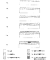
図1は、レーザー相互接続でOOEDを製造する方法の重要なステップを示す。基板が設けられている。 FIG. 1 illustrates the key steps of a method for manufacturing OOED with laser interconnects. A substrate is provided.
基板はステップ1aにおいて絶縁層で覆われる。好ましくは、堆積は、反応CVD、スピンコーティング、スパッタリング、VTE(真空熱蒸着)、スプレー、インクジェット、ブレードコーティングで行う。このステップの後、ステップ1bでSMLが堆積される。この所望の構造は、所望の領域にのみ層を堆積することによって、または、全領域上に層を堆積することによって、また、後部パターニングによって得ることができる(1c)。限定されないが、このような方法の例は、VTEによるシャドーマスク堆積、スパッタリングによるシャドーマスク堆積、後部パターニングでの堆積、下のパターニングされた層の後部リフトオフでの堆積がある。SMLのパターンは、少なくとも2つの電気的に切断された領域が形成されるようなパターンである。図1および図3の領域を左から右へ見て、領域A(RA)は、底部電極を部分的に形成し、領域B(RB)は最上位電極の電気接続部を形成し、さらに別の領域Aは、別のOOEDの底部電極を部分的に形成する。 The substrate is covered with an insulating layer in step 1a. Preferably, the deposition is performed by reactive CVD, spin coating, sputtering, VTE (vacuum thermal evaporation), spray, ink jet, blade coating. After this step, SML is deposited in step 1b. This desired structure can be obtained by depositing a layer only in the desired area, or by depositing a layer over the entire area, and by back patterning (1c). Examples of such methods include, but are not limited to, shadow mask deposition by VTE, shadow mask deposition by sputtering, back pattern deposition, and back lift off deposition of the underlying patterned layer. The SML pattern is such that at least two electrically cut regions are formed. Looking at the regions of FIGS. 1 and 3 from left to right, region A (RA) partially forms the bottom electrode, region B (RB) forms the electrical connection of the top electrode, and Region A partially forms the bottom electrode of another OOED.
図1のステップ1dで、OSLは、従来技術によって堆積される。OSLは、小さい分子材料、小さい分子層、ポリマー層、あるいは、小さい分子とポリマーとの層を有する。TCLは、ステップ1eでOSL上に堆積される。TCLの堆積は、好ましくは、VTEまたはスパッタリングで行われ、本質的にマスクなしで行われる。 In step 1d of FIG. 1, the OSL is deposited by conventional techniques. OSL has a small molecular material, a small molecular layer, a polymer layer, or a layer of small molecules and polymers. TCL is deposited on the OSL in step 1e. TCL deposition is preferably done by VTE or sputtering, essentially without a mask.
SMLとTCLとの間の少なくとも一つの電気的相互接続部は、ステップ1fにおいてレーザーで形成され、最上位電極を領域(RB)に電気的に相互接続する。 At least one electrical interconnect between the SML and the TCL is formed with a laser in step 1f to electrically interconnect the top electrode to the region (RB).
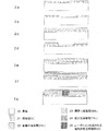
図2は、レーザー相互接続でOOEDを生成する方法のステップを示す。この代替実施形態は、基板の電気導電特性を利用する。金属基板が設けられる。これは、あるいは、金属層でコーティングされた非導電性基板とすることもできる。金属基板の例は、上述してある。限定されないが、コーティングされた非導電性基板の例は、アルミニウムでコーティングされたガラス、銅でコーティングされたガラス、銅でコーティングされたPET(Polyethylene terephthalate)、銀でコーティングされたポリイミドである。 FIG. 2 shows the steps of a method for generating an OOED with a laser interconnect. This alternative embodiment takes advantage of the electrical conductivity characteristics of the substrate. A metal substrate is provided. This can alternatively be a non-conductive substrate coated with a metal layer. Examples of metal substrates are described above. Non-limiting examples of coated non-conductive substrates are glass coated with aluminum, glass coated with copper, PET (Polyethylene terephthalate) coated with copper, and polyimide coated with silver.
ステップ2aは、基板上に絶縁層を堆積することである。堆積は、パターニングする方法で行える。オプションとしては、堆積は、パターニングしない方法で行い、層は後でパターニングされる。好ましい態様は、フォトレジストでもある絶縁層であり、フォトリソグラフィーでパターニングすることである。他の好ましい態様は、絶縁層がレーザーアブレーションでパターニングされることである。 Step 2a is to deposit an insulating layer on the substrate. Deposition can be performed by a patterning method. Optionally, the deposition is performed in a non-patterned manner and the layer is later patterned. A preferred embodiment is an insulating layer that is also a photoresist and is patterned by photolithography. Another preferred embodiment is that the insulating layer is patterned by laser ablation.
SMLは、ステップ2bで堆積される。また、SMLは、互いに電気的に切断された領域(RA)と(RB)とで規定する必要がある。SMLのパターンは、堆積中に規定できる。あるいは、付加的なステップ2cによりパターニングすることもできる。領域(RA)と(RB)の機能は、図1で説明したものと同じである。 SML is deposited in step 2b. Further, the SML needs to be defined by regions (RA) and (RB) that are electrically disconnected from each other. The SML pattern can be defined during deposition. Alternatively, it can be patterned by an additional step 2c. The functions of the areas (RA) and (RB) are the same as those described in FIG.
あるいは、絶縁層とSMLとは、パターンなしで堆積され、両層は、一つのステップでパターニングされる。この場合、少なくとも一つの領域(RB)(図2、ステップ2dの中央のSML領域)も除去される。両層をパターニングする好ましい態様は、絶縁層がフォトレジストでもある場合には、リフトオフにて行う。他の好ましい態様は、両層がレーザーアブレーションでパターニングされることである。 Alternatively, the insulating layer and SML are deposited without a pattern, and both layers are patterned in one step. In this case, at least one region (RB) (FIG. 2, the central SML region of step 2d) is also removed. A preferred mode of patterning both layers is lift-off when the insulating layer is also a photoresist. Another preferred embodiment is that both layers are patterned by laser ablation.
図2eは、図1のステップ1dに対応する。図2fは、図1のステップ1eに対応する。 FIG. 2e corresponds to step 1d of FIG. FIG. 2f corresponds to step 1e of FIG.
ステップ2gは、相互接続ステップであり、ここではTCLと(RB)の間で電気的相互接続が行われる。あるいは、領域(RB)が除去された場合は、金属基板に対し、あるいは、非導電性基板上に設けられた導電層に対し、TCLの相互接続が直接に行われる。 Step 2g is an interconnection step, where an electrical interconnection is made between TCL and (RB). Alternatively, when the region (RB) is removed, TCL interconnections are made directly to the metal substrate or to the conductive layer provided on the non-conductive substrate.
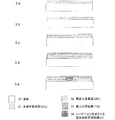
図3は、非導電性基板上にOOEDを製造する方法を示す。非導電性基板(ガラス、プラスチック、その他)が設けられている。図1および図2で説明した通り、ステップ3aにおいて非導電性基板上にSMLが堆積される。SMLが、構造化して堆積されない場合には、オプションとして、その後にパターニングステップ(3b)を行うことができる。 FIG. 3 illustrates a method for manufacturing OOED on a non-conductive substrate. A non-conductive substrate (glass, plastic, etc.) is provided. As described in FIGS. 1 and 2, SML is deposited on the non-conductive substrate in step 3a. If the SML is not structured and deposited, an optional patterning step (3b) can be performed.
図1で説明した通り、図3のSMLは、少なくとも2つの領域を有している。図3cは、図1のステップ1dに対応する。図3dは、図1のステップ1eに対応する。図3eは、図1のステップ1fに対応する。 As described with reference to FIG. 1, the SML in FIG. 3 has at least two regions. FIG. 3c corresponds to step 1d of FIG. FIG. 3d corresponds to step 1e of FIG. FIG. 3e corresponds to step 1f of FIG.
OOEDは、領域(RA)と(RB)との間に電圧を印加する電力供給によって電力の供給を受ける発光装置である。もしOOEDが有機光起電装置であれば、外部の電気接触は、領域(RA)と(RB)に接続することになる。 The OOED is a light-emitting device that is supplied with power by supplying power that applies a voltage between the regions (RA) and (RB). If OOED is an organic photovoltaic device, external electrical contact will connect to regions (RA) and (RB).
図4は、平行なストライプに形成されたOOEDの平面図である。図4は、構造化された、平行な、広いほうの領域と狭いほうの領域(それぞれ領域AとBとを設けている)を有する基板40を示している。広いほうの領域は、絶縁層41上に形成されている。SML43上に、パターニングされていないOSL42が堆積される。次いで、OSL42上にTCL44が堆積される。狭いほうのSML領域43は、電気的相互接続部45を介してTCL44に電流を供給する領域(RB)である。基板が金属基板の場合や、また、基板が金属層でコーティングされていて、TCL44と基板40との間に相互接続部45を直接形成できる場合は、領域(RB)は不要である。 FIG. 4 is a plan view of an OOED formed in parallel stripes. FIG. 4 shows a substrate 40 having a structured, parallel, wide and narrow area (providing areas A and B, respectively). The wider region is formed on the insulating layer 41. On the SML 43, an unpatterned OSL 42 is deposited. Next, TCL 44 is deposited on OSL 42. The narrower SML region 43 is a region (RB) that supplies current to the TCL 44 via the electrical interconnection 45. If the substrate is a metal substrate, or if the substrate is coated with a metal layer and the interconnection 45 can be formed directly between the TCL 44 and the substrate 40, the region (RB) is not necessary.
基板50上に絶縁層51とSML52とをパターニングする代替例を図5に示す。ここでは、基板50は、金属基板であるか、あるいは、金属層でコーティングされた基板である。SML52は、絶縁層51の上にだけ形成される。OSLとTCLとは、最上位に堆積される(図示せず)。この実施形態では、TCLの相互接続は、絶縁層51を有しない領域で行われる。 An alternative example of patterning the insulating layer 51 and the SML 52 on the substrate 50 is shown in FIG. Here, the substrate 50 is a metal substrate or a substrate coated with a metal layer. The SML 52 is formed only on the insulating layer 51. OSL and TCL are deposited on top (not shown). In this embodiment, the TCL interconnection is performed in a region where the insulating layer 51 is not provided.
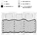
図6は、基板60が設けられる、他の実施形態を示す。基板60は、金属基板であるか、あるいは、金属層でコーティングされた基板である。基板60は、絶縁層61でコーティングされている。絶縁層61は、点64の外側の円で規定されるマトリクス状の穴を形成することでパターニングされている。図面の簡略化のためSMLは図示しないが、OSL62の下に形成され、(同じく点64の外側の円で規定される)絶縁層62と同じ位置での穴で同様にパターニングされている。TCLは、破線で規定される長方形領域に堆積される。相互接続は、レーザーで形成され、黒(塗りつぶし)円64で規定される。 FIG. 6 shows another embodiment in which a substrate 60 is provided. The substrate 60 is a metal substrate or a substrate coated with a metal layer. The substrate 60 is coated with an insulating layer 61. The insulating layer 61 is patterned by forming a matrix-like hole defined by a circle outside the point 64. To simplify the drawing, the SML is not shown, but is formed under the OSL 62 and similarly patterned with holes at the same position as the insulating layer 62 (also defined by a circle outside the point 64). TCL is deposited in a rectangular area defined by a broken line. The interconnect is formed by a laser and is defined by a black (filled) circle 64.
図6では、OOEDは、有機発光装置である場合には、電源に電気的に接続されることができ、あるいは、有機光起電装置の場合には、他の外部回路と電気的に接続されることができる。これらの接続は、SMLの延長部と基板への電気接続部とを介して、または、基板が非導電性の場合には、基板上の導電層を介して行う。 In FIG. 6, the OOED can be electrically connected to a power source in the case of an organic light emitting device, or can be electrically connected to other external circuits in the case of an organic photovoltaic device. Can. These connections are made via SML extensions and electrical connections to the substrate or, if the substrate is non-conductive, via a conductive layer on the substrate.
すべての実施形態で、好ましくは、カプセル化は、相互接続ステップの前に行う。 In all embodiments, preferably the encapsulation is performed before the interconnection step.
以下に、様々な実施例を述べる。特に指定していない限り、以下の堆積技術が各実施例で用いられた。
SMLは、パターニングのためのシャドーマスクを用いるVTEで堆積された。
OSLはVTEで堆積された。
TCLはVTEで堆積されたが、スパッタリングや他の方法でも同様に行える。
カプセル化されていない装置の相互接続ステップは、不活性雰囲気下で行った。
Various embodiments are described below. The following deposition techniques were used in each example unless otherwise specified.
SML was deposited with VTE using a shadow mask for patterning.
OSL was deposited with VTE.
TCL was deposited by VTE, but could be done by sputtering or other methods as well.
The interconnect step of the unencapsulated device was performed under an inert atmosphere.
パターニングされた非導電性層
実施例ではしばしば、以下のようにして形成される、パターニングされた非導電性層を用いる。2.3μmの厚みの光学的に規定可能なポリイミド層(HD microsystems製HD-8820)が、3500rpmのスピンコーティングによって基板上に堆積された。ポリイミド層は120℃で3分加熱された。50秒間光パターンに露光することでパターンが規定され、120秒間現像され、180℃で30分間加熱された。
Patterned Non-Conducting Layer Examples often use a patterned non-conducting layer formed as follows. An optically definable polyimide layer (HD-8820 from HD Microsystems) with a thickness of 2.3 μm was deposited on the substrate by spin coating at 3500 rpm. The polyimide layer was heated at 120 ° C. for 3 minutes. The pattern was defined by exposure to a light pattern for 50 seconds, developed for 120 seconds, and heated at 180 ° C. for 30 minutes.
〔実施例1 電気的相互接続部を有する有機発光装置〕
100mm×100mmのガラス基板が用意された。このガラス基板上に90mm×78mmの金属層SMLが堆積された。金属層は、平行なストライプを形成してパターニングされた。広いストライプ(RA−領域A)は90mm×20mmの寸法を有し、狭いストライプ(RB−領域B)は90mm×3mmの寸法を有する。ストライプ間には1mmのスペースが常にある。ストライプは、以下の構成で形成された、すなわち、(RB)−3×((RA)−(RB))である(「−」は、横方向の層の分離を示す)。この構成は、図4のSMLと似ている。
Example 1 Organic Light-Emitting Device Having Electrical Interconnection
A glass substrate of 100 mm × 100 mm was prepared. A 90 mm × 78 mm metal layer SML was deposited on the glass substrate. The metal layer was patterned to form parallel stripes. The wide stripe (RA-region A) has a dimension of 90 mm × 20 mm, and the narrow stripe (RB-region B) has a dimension of 90 mm × 3 mm. There is always a 1 mm space between the stripes. The stripes were formed with the following configuration: (RB) -3 × ((RA)-(RB)) ("-" indicates lateral layer separation). This configuration is similar to the SML in FIG.
以下の層を有する、パターニングされていない80mm×78mmのOSLが、以下のようにしてSML上に堆積された。すなわち、F4TCNQにてドーピングされた50nmの厚みのNPD層、ドーピングされていない10nmの厚みのNPD層、蛍光放射体でドーピングされた青色発光ホスト層、10nmのBPhen、Csでドーピングされた60nmのBPhenである。そして、20nmのAg層が、TCLとして堆積された。 An unpatterned 80 mm x 78 mm OSL with the following layers was deposited on the SML as follows. That is, a 50 nm thick NPD layer doped with F4TCNQ, an undoped 10 nm thick NPD layer, a blue light emitting host layer doped with fluorescent emitters, 10 nm BPhen, 60 nm BPhen doped with Cs It is. A 20 nm Ag layer was then deposited as TCL.
OSL、(RA)、TCL間の重なりが、底部電極を形成する。(RB)は、最上位電極へのフィードコンタクトである。 The overlap between OSL, (RA) and TCL forms the bottom electrode. (RB) is a feed contact to the uppermost electrode.
領域(RB)上にレーザーパルスを印加することによって電気的相互接続部を形成した。レーザーは、最上位側から(言い換えれば、基板を介さずに)印加した。この実施例で用いたレーザーは、1064nmで作動するDPSS Nd:YAGレーザーである。相互接続点が、各領域(RB)の80mmの長さ(この長さは、OSLと重なる。)にわたって、1点/250μmの線密度で形成された。 An electrical interconnect was formed by applying a laser pulse over the region (RB). The laser was applied from the uppermost side (in other words, not through the substrate). The laser used in this example is a DPSS Nd: YAG laser operating at 1064 nm. Interconnect points were formed at a linear density of 1 point / 250 μm over the 80 mm length of each region (RB) (this length overlaps the OSL).
最後に、装置を試験するために、(OSLと重ならない)領域(RB)の先端を電力供給部の負極に接続し、領域(RA)の先端を電力供給部の正極に接続した。この装置は、並列に接続された3つの発光領域を有するように製造された。すべての3つの領域が、高輝度と、発光表面にわたっての発光強度の高い同質性とを持って作動した。 Finally, to test the device, the tip of the region (RB) (not overlapping OSL) was connected to the negative electrode of the power supply unit, and the tip of the region (RA) was connected to the positive electrode of the power supply unit. This device was manufactured to have three light emitting areas connected in parallel. All three regions operated with high brightness and high homogeneity of emission intensity across the emitting surface.
〔実施例2 金属基板と電気的相互接続部との上の有機発光装置〕
横方向の寸法が100mm×100mmの、0.8mmの厚みのステンレス鋼板が基板として用意された。2.3μmの厚みのポリイミド層(HD microsystems製のPI2555)が、3500rpmのスピンコーティングによって金属基板上に堆積され、180℃で30分間加熱された。実施例1のステップが繰り返された(ガラス基板を用意するという1番目のステップを除く)。装置は、実施例1同様、期待通りに作動した。
Example 2 Organic Light Emitting Device Over Metal Substrate and Electrical Interconnection
A stainless steel plate having a thickness of 0.8 mm and a lateral dimension of 100 mm × 100 mm was prepared as a substrate. A 2.3 μm thick polyimide layer (PI2555 from HD microsystems) was deposited on the metal substrate by spin coating at 3500 rpm and heated at 180 ° C. for 30 minutes. The steps of Example 1 were repeated (except for the first step of preparing a glass substrate). The device worked as expected as in Example 1.
〔実施例3 金属基板と電気的相互接続部との上の有機発光装置〕
横方向の寸法が100mm×100mmの、0.8mmの厚みのステンレス鋼板が基板として用意された。上述のように、パターニングされた非導電性層が堆積された。図4に示すように、Agの100nmの厚みのSML層がポリイミド層(RA)と露出した基板領域(RB)との上に堆積された。この場合、フィードコンタクトは、基板自身(領域(RB))で形成される。実施例1と同じくOSLとTCLとの堆積処理が繰り返された。
Example 3 Organic Light Emitting Device Over Metal Substrate and Electrical Interconnection
A stainless steel plate having a thickness of 0.8 mm and a lateral dimension of 100 mm × 100 mm was prepared as a substrate. A patterned non-conductive layer was deposited as described above. As shown in FIG. 4, a 100 nm thick SML layer of Ag was deposited on the polyimide layer (RA) and the exposed substrate region (RB). In this case, the feed contact is formed by the substrate itself (region (RB)). Similar to Example 1, the deposition process of OSL and TCL was repeated.
領域(RB)上にレーザーパルスを印加することによって電気的相互接続部を形成した。レーザーは、最上位側から(言い換えれば、基板を介さずに)印加した。この実施例で用いたレーザーは、1064nmで作動するパルスNd:YVO4レーザーである。相互接続点が、各領域(RB)の80mmの長さ(この長さは、OSLと重なる。)にわたって、1点/250μmの線密度で形成された。 An electrical interconnect was formed by applying a laser pulse over the region (RB). The laser was applied from the uppermost side (in other words, not through the substrate). The laser used in this example is a pulsed Nd: YVO4 laser operating at 1064 nm. Interconnect points were formed at a linear density of 1 point / 250 μm over the 80 mm length of each region (RB) (this length overlaps the OSL).
この方法は、所望の効果を奏する結果となった。 This method resulted in the desired effect.
〔実施例4 金属基板と電気的相互接続部との上の有機発光装置〕
以下のように変更して、実施例3を繰り返した。ポリイミド層は、図5に示すようにパターニングされた。SMLは、金属基板と接触するようには堆積されず、図5に示すように、ポリイミド層上にだけ堆積されるようにパターニングされた。
Example 4 Organic Light Emitting Device Over Metal Substrate and Electrical Interconnection
Example 3 was repeated with the following changes. The polyimide layer was patterned as shown in FIG. The SML was not deposited to contact the metal substrate, but was patterned to be deposited only on the polyimide layer, as shown in FIG.
〔実施例5 電気的相互接続部を有する有機発光装置〕
横方向の寸法が100mm×100mmの、0.8mmの厚みのステンレス鋼板が基板として用意された。上述のように、ポリイミド層からなるパターニングされた非導電性層が堆積された。マトリクス状の穴として、基板を露出するためにポリイミド層がパターニングされた。マトリクスの行と列との間のスペースは20mmであり、各穴の直径は1mmである。ポリイミド層上に、Agからなる、100nmの厚みのSML層が堆積された。
Example 5 Organic Light Emitting Device Having Electrical Interconnection
A stainless steel plate having a thickness of 0.8 mm and a lateral dimension of 100 mm × 100 mm was prepared as a substrate. As described above, a patterned non-conductive layer consisting of a polyimide layer was deposited. As a matrix hole, the polyimide layer was patterned to expose the substrate. The space between the matrix rows and columns is 20 mm and the diameter of each hole is 1 mm. A 100 nm thick SML layer made of Ag was deposited on the polyimide layer.
穴のSMLと絶縁層とを除去するために、周波数二重化Nd:YAGレーザーが用いられ、基板を露出した。あるいは、複雑さは増すが、SMLをパターニングするために、光で規定可能なポリイミド層や付加的なフォトレジストを用いることもできる。 A frequency doubled Nd: YAG laser was used to remove the hole SML and the insulating layer, exposing the substrate. Alternatively, a light-definable polyimide layer or additional photoresist can be used to pattern the SML, albeit with increased complexity.
実施例1で述べたように、OSLとTCLとの堆積ステップが繰り返された。 As described in Example 1, the OSL and TCL deposition steps were repeated.
3つの隣接する相互接続部を形成する各穴の中央にレーザーパルスを印加することによって、電気的相互接続部を形成した。レーザーは、最上位側から(言い換えれば、基板を介さずに)印加した。この実施例で用いたレーザーは、1064nmで作動するパルスNd:YAGレーザーであり、パルス間隔は8psであった。 Electrical interconnects were formed by applying a laser pulse in the center of each hole forming three adjacent interconnects. The laser was applied from the uppermost side (in other words, not through the substrate). The laser used in this example was a pulsed Nd: YAG laser operating at 1064 nm and the pulse interval was 8 ps.
本方法では、図6で示される装置が得られた。OLEDは、装置の表面上において、発光の高い同質性を示した。 In this method, the apparatus shown in FIG. 6 was obtained. The OLED showed high homogeneity of light emission on the surface of the device.
〔実施例6 電気的相互接続部を有する、カプセル化された有機発光装置〕
実施例5が繰り返された。ただし、装置は、ガラスカバーでカプセル化され、また、電気的相互接続を行うステップはカプセル化の後に行われ、ガラスカバーを介してレーザーが照射された。利点は、相互接続ステップが空気中で行えることである。一方、カプセル化されていないサンプルに対しては、このようなサンプルは酸素、湿気、ほこりに敏感なであるため、該ステップは、不活性の雰囲気下で行う必要がある。
Example 6 Encapsulated Organic Light-Emitting Device with Electrical Interconnection
Example 5 was repeated. However, the device was encapsulated with a glass cover, and the electrical interconnection step was performed after encapsulation and the laser was irradiated through the glass cover. The advantage is that the interconnection step can be done in air. On the other hand, for unencapsulated samples, such steps are sensitive to oxygen, moisture, and dust, so the step must be performed in an inert atmosphere.
〔実施例7 ガラス上に電気的相互接続部を有する、カプセル化された有機発光装置〕
以下のように修正した上で、実施例6が繰り返された。500nmの、比較的厚い、パターニングされていない金属層(TML)が、金属基板の代わりに用いられた。
Example 7 Encapsulated Organic Light Emitting Device Having Electrical Interconnection on Glass
Example 6 was repeated with the following modifications. A relatively thick, unpatterned metal layer (TML) of 500 nm was used in place of the metal substrate.
〔実施例8 マスクのない堆積を行った有機発光装置〕
横方向の寸法が100mm×100mmの、0.8mmの厚みのステンレス鋼板が基板として用意された。2.3μmの厚みのポリイミド層(HD microsystems製のPI2555)が、3500rpmのスピンコーティングによって金属基板上に堆積され、180℃で30分間加熱された。ポリイミド層上に、Agからなる、100nmの厚みのSML層が堆積された。
Example 8 Organic Light-Emitting Device Performed Deposition without Mask
A stainless steel plate having a thickness of 0.8 mm and a lateral dimension of 100 mm × 100 mm was prepared as a substrate. A 2.3 μm thick polyimide layer (PI2555 from HD microsystems) was deposited on the metal substrate by spin coating at 3500 rpm and heated at 180 ° C. for 30 minutes. A 100 nm thick SML layer made of Ag was deposited on the polyimide layer.
ポリイミド層に穴が形成された。また、一度に両層を除去するために、Nd:YAGレーザーを用いてSMLがパターニングされた。 Holes were formed in the polyimide layer. Also, SML was patterned using a Nd: YAG laser to remove both layers at once.
実施例1同様に、OSLとTCLとの堆積ステップが繰り返された。本質的にはパターニングされなかったが、電源から電極へと電気接続部が形成されるように領域を規定した。 As in Example 1, the OSL and TCL deposition steps were repeated. Although not essentially patterned, the region was defined such that an electrical connection was made from the power source to the electrode.
相互接続部を形成する各穴の中央にレーザーパルスを印加することによって、電気的相互接続部を形成した。レーザーは、最上位側から(言い換えれば、基板を介さずに)、光学配置を用いて印加した(ただし、光学配置なしで行うこともできる)。相互接続部は、マトリクス形式に対して1/mmとなった。 An electrical interconnect was formed by applying a laser pulse to the center of each hole forming the interconnect. The laser was applied from the uppermost side (in other words, not through the substrate) using an optical arrangement (although it can be performed without the optical arrangement). The interconnect was 1 / mm relative to the matrix format.
OELDは、非常に高い同質性を示して、期待通りに作動した。この高度に簡略化された方法を用いれば、マスクやフォトリソグラフィーによるパターニングステップなしで、再面積の有機発光装置を形成することができる。 OELD showed very high homogeneity and worked as expected. By using this highly simplified method, a re-area organic light-emitting device can be formed without a patterning step using a mask or photolithography.
〔有機光起電装置〕
単一で、大面積の有機光セルの形式で、有機光起電装置を製造した。横方向の寸法が100mm×100mmの、0.8mmの厚みのステンレス鋼板が基板として用意された。上述の通りに、ポリイミドからなる、パターニングされた非導電性層が堆積された。マトリクス状の穴として、基板を露出するためにポリイミド層がパターニングされた。マトリクスの行と列との間のスペースは20mmであり、各穴の直径は1mmである。ポリイミド層上に、Agからなる、100nmの厚みのSML層が堆積された。
[Organic photovoltaic device]
Organic photovoltaic devices were manufactured in the form of a single, large area organic photocell. A stainless steel plate having a thickness of 0.8 mm and a lateral dimension of 100 mm × 100 mm was prepared as a substrate. A patterned non-conductive layer made of polyimide was deposited as described above. As a matrix hole, the polyimide layer was patterned to expose the substrate. The space between the matrix rows and columns is 20 mm and the diameter of each hole is 1 mm. A 100 nm thick SML layer made of Ag was deposited on the polyimide layer.
穴のSMLと絶縁層とを除去するために、周波数二重化Nd:YAGレーザーが用いられ、基板を露出した。あるいは、複雑さは増すが、SMLをパターニングするために、光で規定可能なポリイミド層や付加的なフォトレジストを用いることもできる。 A frequency doubled Nd: YAG laser was used to remove the hole SML and the insulating layer, exposing the substrate. Alternatively, a light-definable polyimide layer or additional photoresist can be used to pattern the SML, albeit with increased complexity.
以下の層がOSLとして堆積された。
ITO上のシャドーマスクを介して、10nmの厚みの、5%(モル濃度)のpドーピングされたCuPc(Cu-Phthalocyanine)層が堆積された。
ドーピングされた上記CuPc層の上に、10nmの厚みの、ドーピングされていないCuPc層が堆積された。
C60とCuPcとのモル濃度比2:1で、30nmの厚みの、フラーレンC60とCuPcとの混合層が堆積された。
上記混合層の最上位に、40nmの厚みのC60層が堆積された。
上記C60層の最上位に、10nmの厚みのBPhen(4,7-diphyenyl-1,10-phenanthroline)層が堆積された。
The following layers were deposited as OSL.
A 10% thick 5% (molar) p-doped CuPc (Cu-Phthalocyanine) layer was deposited through a shadow mask on ITO.
On top of the doped CuPc layer, an undoped CuPc layer having a thickness of 10 nm was deposited.
A mixed layer of fullerene C60 and CuPc with a thickness of 30 nm was deposited at a molar concentration ratio of C60 to CuPc of 2: 1.
A C60 layer with a thickness of 40 nm was deposited on top of the mixed layer.
A BPhen (4,7-diphyenyl-1,10-phenanthroline) layer having a thickness of 10 nm was deposited on the top of the C60 layer.
20nmのAgがTCLとして堆積された。 20 nm of Ag was deposited as TCL.
3つの隣接する、穴同士の相互接続部を形成する外側の穴の中央にレーザーパルスを印加することによって、電気的相互接続部を形成した。レーザーは、最上位側から(言い換えれば、基板を介さずに)印加した。この実施例で用いたレーザーは、1064nmで作動するパルスNd:YAGレーザーであった。 The electrical interconnect was formed by applying a laser pulse to the center of the outer hole forming the three adjacent, hole-to-hole interconnects. The laser was applied from the uppermost side (in other words, not through the substrate). The laser used in this example was a pulsed Nd: YAG laser operating at 1064 nm.
この装置は、特徴的な高い直列抵抗を持った電流電圧曲線を示した。実験的な特徴付けの後、(マトリクス−直交格子−フォーマットにおける)他のすべての穴の中へ電気的相互接続を行ったところ、直列抵抗が著しく減少した。図6は、このような装置の幾何学を示す。短絡回路電流が、100%を超えて改善した。 This device exhibited a current-voltage curve with a characteristic high series resistance. After experimental characterization, electrical interconnects into all other holes (in matrix-orthogonal lattice-format) resulted in a significant reduction in series resistance. FIG. 6 shows the geometry of such a device. Short circuit current improved over 100%.
以下に、直列の相互接続部を有する有機電子装置の好ましい実施形態について述べる。図7ないし図13を参照する。 In the following, preferred embodiments of organic electronic devices having series interconnections are described. Please refer to FIG. 7 to FIG.
矢印は、有機発光装置である装置の場合に光が発射される方向を示す。これらの矢印は、装置が、最上位発光(吸収)、底部発光(吸収)、または完全に透明であるか、という、装置の様態を示すために用いられている。 The arrow indicates the direction in which light is emitted in the case of a device that is an organic light emitting device. These arrows are used to indicate the mode of the device, whether it is top emission (absorption), bottom emission (absorption), or completely transparent.
図7aは、従来技術に係る、直列に接続された個々の装置を有する、底部発光型の有機発光装置を示す。図7aは、透明基板70aの上の層構造を示しており、該構造は、透明底部電極71a、少なくとも一つの有機半導体層72a、反射最上位電極73aを有している。上記の少なくとも一つの有機半導体層72aと最上位電極73aとは、シャドーマスクやインクジェットプリンティングなどによって直接パターニングされる必要がある。矢印は、OLEDである装置の場合に光が発射される方向を示している。この方向は、光起電装置の光の吸収とは逆である。
FIG. 7a shows a bottom-emitting organic light-emitting device with individual devices connected in series according to the prior art. FIG. 7a shows the layer structure on the
図7bは、基板70b上に、あらかじめパターニングされた底部電極71bと、電気的に絶縁するセパレータ75bとを有する、底部発光型の装置を示す。有機層72bと最上位電極73bとは、シャドーマスクなしで形成されている。個々の装置の分離は、層の堆積中に、電気的に絶縁するセパレータ75bによって行われる。最上位電極と底部電極との電気的無機結晶光起電装置とも称される、直列の電気的相互接続部74bは、レーザー処理によって行われる。
FIG. 7b shows a bottom-emitting device having a pre-patterned
図8は、最上位発光装置(または最上位吸収光起電装置)であり、基板80の上の底部電極81と、底部電極81と最上位電極83との間の少なくとも一つの有機半導体層82と、最上位電極83とを有する層構造を備えている。ここでは、最上位電極83は透明であり、基板80および/または底部電極81は反射性である。個々の装置の分離は、層の堆積中に、電気的に絶縁するセパレータ85によって行われる。直列の電気的相互接続部84は、レーザーによって形成される。
FIG. 8 shows a top light emitting device (or top absorption photovoltaic device), which is a
図9は、電極91・93間に少なくとも一つの有機半導体層92を有する透明な装置を示している。ここでは、最上位電極93、底部電極91、基板90が透明である。絶縁セパレータ95と、直列の電気的相互接続部94とが、個々の装置(i+1、i、i−1、…)の直列の接続部を提供している。
FIG. 9 shows a transparent device having at least one
図10は、直列接続された複数の個々の装置(カラム…、i−1、i、i+1)の配列を示している。このカラムは、平行(行)(row)に接続されている。図10は、パターニングされた底部電極101、絶縁セパレータ102、直列の電気的相互接続部104を示している。黒い線(104)は、どこにレーザーを印加するかを示している。明らかに、電気的相互接続部は、最上位電極と底部電極とが形成されている所にだけ形成されている。これらのカラムは、導電層105・106によって平行に接続されるようにすることができる。あるいは、これらのカラムは、グループごとに、あるいは個々に、駆動されるようにすることもできる。これの代わりに、あるいは追加として、底部電極を形成する層は、隣接カラムの間で連続するようにパターニングされることもできる。一つの行の底部電極は、オプションとして、単一の層(例えばストライプ)で形成されるようにすることもできる。最上位電極をも提供する層103は、一部分だけ示している(明確化のため)。
FIG. 10 shows an arrangement of a plurality of individual devices (columns..., I−1, i, i + 1) connected in series. This column is connected in parallel. FIG. 10 shows the patterned
層106は、最上位に形成され、有機層の堆積前に底部電極に電気的に接触する。あるいは、またはオプションとして、電気的相互接続部107は、導電層106と底部電極との間で内部接続部を供給するのに用いることができる。他のバリエーションも可能である。例えば、導電層106は、底部電極と重ならない。そして、最上位電極をも形成する最上位の導電層は、必要な電気的相互接続部を加えて、必要な電気経路を供給する。導電層105と他の実施形態についても同じように考えることができる。導電層105は、オプションとして、最上位電極層の延長とすることができ、有機層の上に形成することができる(これも、他の実施形態に応用できる)。
図11は、直列接続された複数の個々の装置(カラム…、i−1、i、i+1)の配列を示している。この列は、平行(行)(row)に接続されている。図11は、パターニングされた底部電極111、絶縁セパレータ112、直列の電気的相互接続部114を示している。これらのカラムは、導電層115・116によって平行に接続されるようにすることができる。最上位電極をも提供する層113は、一部分だけ示している(明確化のため)。この実施形態では、絶縁セパレータ112は領域112・117にパターニングされている。ここでは、領域117(カラムに平行)は、発光領域を規定するのに用いられている。これの代わりに、あるいは追加として、底部電極111を形成する層は、隣接カラムの間で連続するようにパターニングされることもできる。一つの行の底部電極111は、オプションとして、単一の層(例えばストライプ)で形成されるようにすることもできる。
FIG. 11 shows an arrangement of a plurality of individual devices (columns..., I−1, i, i + 1) connected in series. This column is connected in parallel (row). FIG. 11 shows the patterned
図12は、基板120、底部電極121、少なくとも一つの有機層122、最上位電極123を有する層構造を示している。少なくとも一つの有機層122と最上位電極123とを2つの領域に分離するために絶縁セパレータ125が用いられている。絶縁セパレータ125は、好ましくは、円錐(マッシュルーム)形状である。これは、異なるエッチング速度(低い位置の部位ほど、高いエッチング速度とする必要がある。)で2つのフォトレジストから絶縁セパレータ125を形成することによって実現可能である。
FIG. 12 shows a layer structure having a
図13は、本発明の全実施形態に用いうる電気的相互接続部の形態を示している。図13は、基板130、底部電極131、少なくとも一つの有機層132、最上位電極133を有する層構造を示している。閉じたOSLを介して、常に電気的相互接続がなされている。OSLは、閉じた層で形成され、ICは、OSLを介して、2つの対向する電極の局所的接続部を提供している。上述のようにしてレーザー法にて電気的相互接続部を形成した後、最上位電極は底部電極に直接接触する。最上位電極を形成する層は、必ずしも、図13に示すように遮断する必要はない。
FIG. 13 shows a form of electrical interconnection that can be used in all embodiments of the present invention. FIG. 13 shows a layer structure having a
以下に、装置の例を参照してさらなる実施形態について述べる。 In the following, further embodiments will be described with reference to examples of devices.
〔有機発光装置の例〕
以下の用語を用いる。「Spiro-TTB」は、octap-tolyl-9,9'-spirobi[fluorene]-2,2',7,7'-tetraamine-2,2',7,7'-tetrakis(N,N-di-p-methylphenylamino)-9,9'-spirobifluoreneである。「F4TCNQ」は、2,3,5,6-Tetrafluor-7,7,8,8-tetracyanochinodimethanである。「Spiro-TAD」は、2,2',7,7'-Tetrakis(N,N-diphenylamino)-9,9'-spirobifluoreneである。「Ir(ppy)3」は、tris(2-phenylpyridine) iridiumである。「TPBI」は、1,3,5-Tris(1-phenyl-1H-benzimidazol-2-yl)benzeneである。「BPhen」は、2,9-Bis(naphthalen-2-yl)-4,7-diphenyl-1,10-phenanthrolineである。
[Example of organic light-emitting device]
The following terms are used. "Spiro-TTB" is octap-tolyl-9,9'-spirobi [fluorene] -2,2 ', 7,7'-tetraamine-2,2', 7,7'-tetrakis (N, N-di -p-methylphenylamino) -9,9'-spirobifluorene. “F4TCNQ” is 2,3,5,6-Tetrafluor-7,7,8,8-tetracyanochinodimethan. “Spiro-TAD” is 2,2 ′, 7,7′-Tetrakis (N, N-diphenylamino) -9,9′-spirobifluorene. “Ir (ppy) 3” is tris (2-phenylpyridine) iridium. “TPBI” is 1,3,5-Tris (1-phenyl-1H-benzimidazol-2-yl) benzene. “BPhen” is 2,9-Bis (naphthalen-2-yl) -4,7-diphenyl-1,10-phenanthroline.
横寸法100mm×100mm、厚み0.8mmのガラス基板が基板として用意された。このガラス基板は、あらかじめパターニングされたITO層を有し、横寸法80mm×9.5mm、間隔500μmになるよう、8つのストライプにパターニングされた。ただし、装置に電源を供給するのに用いられる基板の端(A)の延長部分を有する1番目のストライプはこれに当てはまらない。 A glass substrate having a lateral dimension of 100 mm × 100 mm and a thickness of 0.8 mm was prepared as a substrate. This glass substrate had an ITO layer patterned in advance, and was patterned into eight stripes so as to have a lateral dimension of 80 mm × 9.5 mm and an interval of 500 μm. However, this is not the case with the first stripe having an extension of the edge (A) of the substrate used to power the device.
上述のようにして、パターニングされた非導電性層が堆積された。各パターニングされたITOストライプの一方の端から300μm離れた所に絶縁セパレータを形成した。絶縁セパレータと上記端との間の300μmの領域は、最上位電極と底部電極との接続部に用いられる。絶縁セパレータは、7行、82mmの長さとなるように形成された。 A patterned non-conductive layer was deposited as described above. An insulating separator was formed at a distance of 300 μm from one end of each patterned ITO stripe. The 300 μm region between the insulating separator and the end is used for the connection between the top electrode and the bottom electrode. The insulating separator was formed to have a length of 7 rows and 82 mm.
VTEによって、有機半導体層の積層が堆積された。この堆積は、装置に電源を供給するのに用いられる基板の端の延長部分を有する1番目のストライプを除いて、ITOストライプを完全に覆う82mm×82mmの領域に対し、行われた。有機層の積層は以下の層で行われた。
穴移送層:78nmのSpiro-TTBを、2モル%のF4TCNQでpドーピングした。
電子移送層:10nmのSpiro-TAD。
発光層1,5nmのSpiro-TADを、5モル%のIr(ppy)3でドーピングした。
発光層2,10nmのTPBIを、9モル%のIr(ppy)3でドーピングした。
電子移送層,10nmのBPhen。
電子移送層,30nmのBPhenを、Cs(モル比1:1)でドーピングした。
A stack of organic semiconductor layers was deposited by VTE. This deposition was performed on an 82 mm × 82 mm area that completely covered the ITO stripe, except for the first stripe with the edge extension of the substrate used to power the device. The organic layer was laminated in the following layers.
Hole transport layer: 78 nm Spiro-TTB was p-doped with 2 mol% F4TCNQ.
Electron transfer layer: 10 nm Spiro-TAD.
The light emitting layer was doped with 5 nm% of Ir (ppy) 3 by Spiro-TAD having a wavelength of 1,5 nm.
The luminescent layer 2,10 nm TPBI was doped with 9 mol% Ir (ppy) 3.
Electron transfer layer, 10 nm BPhen.
The electron transport layer, 30 nm BPhen, was doped with Cs (molar ratio 1: 1).
ITOストライプに重なるように、また、基板の端にまで伸びるように、80mm×90mmの領域上に、100nmのアルミニウムからなる最上位電極が堆積された。この端は、端(A)と対向し、外部電源供給層を提供する。 A top electrode made of 100 nm aluminum was deposited on an area of 80 mm × 90 mm so as to overlap the ITO stripe and extend to the edge of the substrate. This end faces the end (A) and provides an external power supply layer.
最上位電極は、所望の位置で絶縁セパレータによって遮断され、個々の装置を電気的に絶縁する。 The top electrode is interrupted by an insulating separator at the desired location to electrically isolate individual devices.
装置は、ガラス基板に接着された硬いガラスカプセルカバーを用いてカプセル化される。このカプセルは、酸素と水分ゲッターとをも有している。 The device is encapsulated using a hard glass capsule cover adhered to a glass substrate. The capsule also has oxygen and a moisture getter.
絶縁セパレータとITOストライプの端との間で7つの行(row)を形成するITOストライプの端にレーザーパルスを印加することによって、最上位電極と底部電極との直列の電気接続部を形成した。この例で用いられたレーザーは、1064nmで作動するパルスNd:YAGレーザーである。レーザー処理は空気中で行った。これは、装置がカプセル化されているからである。カプセル化の前に不活性雰囲気中で行うこともできるが、処理の複雑さが増す。 A series of electrical connections between the top electrode and the bottom electrode was formed by applying a laser pulse to the end of the ITO stripe forming 7 rows between the insulating separator and the end of the ITO stripe. The laser used in this example is a pulsed Nd: YAG laser operating at 1064 nm. Laser treatment was performed in air. This is because the device is encapsulated. Although it can be done in an inert atmosphere prior to encapsulation, the processing complexity increases.
レーザーパルスはカプセルを介して印加されたが、基板を介して印加することもできる。 The laser pulse is applied through the capsule, but can also be applied through the substrate.
有機発光装置は、直列に接続された8つの単一の発光ダイオードを有し、期待通りに動作した。 The organic light emitting device had eight single light emitting diodes connected in series and operated as expected.
ITOストライプの端から100μmの距離の所に絶縁セパレータを形成し、上記の例を繰り返した。電気的相互接続部は、これらの幅100μm、長さ80mmの領域に形成された。この方法では、処理が簡素化されるだけではなく、接続領域を最小化することができる。ITOストライプ間のギャップでさえ、100μmという小さな値を用いることができ、トータルのデッドスペース(接続に使われるが発光しない領域)を300μmより小さい値にまで減少させることができる。 An insulating separator was formed at a distance of 100 μm from the end of the ITO stripe, and the above example was repeated. Electrical interconnects were formed in these 100 μm wide and 80 mm long regions. This method not only simplifies the process, but also minimizes the connection area. Even the gap between ITO stripes can be as small as 100 μm, and the total dead space (area used for connection but not emitting light) can be reduced to a value less than 300 μm.
〔有機光起電装置〕
寸法100mm×100mm、厚み0.8mmのガラス基板が基板として用意された。このガラス基板は、あらかじめパターニングされたITO層を有し、横寸法80mm×9.5mm、間隔500μmになるよう、8つのストライプにパターニングされた。ただし、装置に電源を供給するのに用いられる基板の端(A)の延長部分を有する1番目のストライプはこれに当てはまらない。
[Organic photovoltaic device]
A glass substrate having a size of 100 mm × 100 mm and a thickness of 0.8 mm was prepared as a substrate. This glass substrate had an ITO layer patterned in advance, and was patterned into eight stripes so as to have a lateral dimension of 80 mm × 9.5 mm and an interval of 500 μm. However, this is not the case with the first stripe having an extension of the edge (A) of the substrate used to power the device.
2.3μmの厚みの光学的に規定可能なポリイミド層(HD microsystems製HD-8820)が、スピンコーティングによって基板上に堆積された。ポリイミド層は120℃で3分加熱された。ポリイミド層を50秒間光パターンに露光し、120秒間現像し、180℃で30分間加熱することによって、二重絶縁セパレータ(間隔500μmで平行な2つの絶縁セパレータ)が規定された。二重絶縁セパレータは、パターニングされたITOストライプの一方の端から500μm離れた所に形成された。二重絶縁セパレータと上記端との間の500μmの領域は、直列の電気的相互接続部の接続のために用いられる。二重絶縁セパレータは、7つの二重行、82mmの長さとなるように形成された。 An optically definable polyimide layer (HD-8820 from HD Microsystems) having a thickness of 2.3 μm was deposited on the substrate by spin coating. The polyimide layer was heated at 120 ° C. for 3 minutes. A double insulating separator (two insulating separators parallel to each other with a spacing of 500 μm) was defined by exposing the polyimide layer to a light pattern for 50 seconds, developing for 120 seconds, and heating at 180 ° C. for 30 minutes. The double insulating separator was formed at a distance of 500 μm from one end of the patterned ITO stripe. The 500 μm region between the double insulating separator and the end is used for the connection of series electrical interconnects. The double insulating separator was formed to be 7 double rows and 82 mm long.
VTEによって、有機半導体層の積層が堆積された。この堆積は、装置に電源を供給するのに用いられる基板の端の延長部分を有する1番目のストライプを除いて、ITOストライプを完全に覆う82mm×82mmの領域に対し、行われた。有機層の積層は以下の層で行われた。
厚み10nm、5モル%のpドーピングされたCuPc(Cu-Phthalocyanine)層が、ITOの上にシャドーマスクを介して堆積された。
10nmのドーピングされていないCuPc層が、ドーピングされたCuPc層の上に堆積された。
厚み30nmの、C60:CuPc=2:1のモル比のフラーレンC60とCuPcとの混合層が堆積された。
厚み40nmのC60層が、上記混合層の最上位に堆積された。
10nmのBPhen(4,7-diphyenyl-1,10-phenanthroline)層が、C60層の最上位に堆積された。
A stack of organic semiconductor layers was deposited by VTE. This deposition was performed on an 82 mm × 82 mm area that completely covered the ITO stripe, except for the first stripe with the edge extension of the substrate used to power the device. The organic layer was laminated in the following layers.
A 10 nm thick, 5 mol% p-doped CuPc (Cu-Phthalocyanine) layer was deposited on the ITO via a shadow mask.
A 10 nm undoped CuPc layer was deposited over the doped CuPc layer.
A mixed layer of C60: CuPc = 2: 1 molar ratio of fullerene C60 and CuPc with a thickness of 30 nm was deposited.
A C60 layer with a thickness of 40 nm was deposited on top of the mixed layer.
A 10 nm BPhen (4,7-diphyenyl-1,10-phenanthroline) layer was deposited on top of the C60 layer.
ITOストライプに重なるように、また、基板の端にまで伸びるように、80mm×90mmの領域上に、100nmのアルミニウムからなる最上位電極が堆積された。この端は、端(A)と対向し、外部電源供給層を提供する。 A top electrode made of 100 nm aluminum was deposited on an area of 80 mm × 90 mm so as to overlap the ITO stripe and extend to the edge of the substrate. This end faces the end (A) and provides an external power supply layer.
最上位電極は、所望の位置で二重絶縁セパレータによって遮断され、個々の装置を電気的に絶縁する。 The top electrode is interrupted by a double insulating separator at the desired location to electrically isolate individual devices.
装置は、ガラス基板に接着された硬いガラスカプセルカバーを用いてカプセル化される。このカプセルは、酸素と水分ゲッターとをも有している。 The device is encapsulated using a hard glass capsule cover adhered to a glass substrate. The capsule also has oxygen and a moisture getter.
絶縁セパレータとITOストライプの端との間で7つの行(row)を形成するITOストライプの端にレーザーパルスを印加することによって、直列の電気的相互接続部を形成した。この例で用いられたレーザーは、1064nmで作動するパルスNd:YAGレーザーである。レーザー処理は空気中で行った。これは、装置がカプセル化されているからである。カプセル化の前に不活性雰囲気中で行うこともできるが、処理の複雑さが増す。レーザーパルスは、基板を介して印加してもよい。 A series electrical interconnect was formed by applying a laser pulse to the end of the ITO stripe forming seven rows between the insulating separator and the end of the ITO stripe. The laser used in this example is a pulsed Nd: YAG laser operating at 1064 nm. Laser treatment was performed in air. This is because the device is encapsulated. Although it can be done in an inert atmosphere prior to encapsulation, the processing complexity increases. The laser pulse may be applied through the substrate.
有機光起電装置は、直列に接続された8つの単一の有機光セルを有し、期待通りに動作し、トータルの開回路電圧3.7Vを生み出した。 The organic photovoltaic device had eight single organic photovoltaic cells connected in series and operated as expected, producing a total open circuit voltage of 3.7V.
他のレーザーもテストされた。各異なるレーザーに対するパラメーターは、相互接続部を供給するために容易に調整可能である。 Other lasers were also tested. The parameters for each different laser can be easily adjusted to provide the interconnect.
明細書、請求項、図面の少なくとも一つに記載した特徴は、単独のまたは種々組み合わせられる様々な実施形態における本発明の実現のために重要である。 Features described in at least one of the specification, the claims, and the drawings are important for the realization of the present invention in various embodiments singly or in various combinations.
Claims (19)
第1導電層を形成するステップと、
上記第1導電層の上に有機半導体層を堆積するステップと、
上記有機半導体層の上に第2導電層を堆積するステップと、
接続領域において、上記第1導電層と上記第2導電層との間に電気的短絡を形成するステップであって、この形成は、上記接続領域にレーザー光を照射することによって上記有機半導体層を介して上記第1導電層と上記第2導電層とを電気的に相互接続することによって行うステップとを有している製造方法。 A manufacturing method for forming an electrical interconnect in an organic electronic device, comprising:
Forming a first conductive layer;
Depositing an organic semiconductor layer on the first conductive layer;
Depositing a second conductive layer on the organic semiconductor layer;
Forming a short circuit between the first conductive layer and the second conductive layer in the connection region, wherein the formation includes irradiating the connection region with a laser beam to irradiate the organic semiconductor layer; And a step of electrically interconnecting the first conductive layer and the second conductive layer.
上記第2導電層を第2金属層として堆積するステップと、
のうち少なくとも一つのステップをさらに有する請求項1に記載の製造方法。 Forming the first conductive layer as a first metal layer;
Depositing the second conductive layer as a second metal layer;
The manufacturing method according to claim 1, further comprising at least one step.
基板を形成するステップと、
上記第1導電層を形成するステップによって、上記基板の上に導電性材料からなる導電構造を形成するステップであって、上記導電構造は、底部電極を形成する領域Aと、最上位電極に対するフィードコンタクトを形成する領域Bとを有し、上記領域AおよびBは互いに電気的に切断されている、ステップと、
上記最上位電極を、上記有機半導体層の上に上記第2導電層を堆積するステップによって形成するステップと、
接続領域において、上記最上位電極と上記フィードコンタクトとの間の電気的短絡を形成するステップであって、この形成は、上記接続領域にレーザー光を照射することによって上記有機半導体層を介して上記最上位電極と上記フィードコンタクトとを電気的に相互接続することによって行うステップとを有している請求項1または2に記載の製造方法。 Further comprising forming the organic electronic device as an organic optoelectronic diode, the step comprising:
Forming a substrate;
Forming a conductive structure made of a conductive material on the substrate by forming the first conductive layer, the conductive structure including a region A for forming a bottom electrode and a feed for a top electrode; A region B for forming a contact, wherein the regions A and B are electrically disconnected from each other;
Forming the top electrode by depositing the second conductive layer on the organic semiconductor layer;
Forming a short circuit between the uppermost electrode and the feed contact in the connection region, wherein the formation is performed by irradiating the connection region with laser light through the organic semiconductor layer. The manufacturing method according to claim 1, further comprising a step of electrically connecting the uppermost electrode and the feed contact.
上記基板の上に金属層を形成するステップと、
上記金属層の上に、パターニングされた絶縁層を形成するステップとを有している請求項3に記載の製造方法。 Forming the conductive structure comprises:
Forming a metal layer on the substrate;
The manufacturing method according to claim 3, further comprising: forming a patterned insulating layer on the metal layer.
上記基板の上に金属層を堆積するステップと、
上記金属層をパターニングするステップとを有している請求項3ないし5のいずれか1項に記載の製造方法。 Forming the conductive structure comprises:
Depositing a metal layer on the substrate;
6. The manufacturing method according to claim 3, further comprising a step of patterning the metal layer.
上記基板の上にフォトレジスト材料層を堆積するステップと、
上記フォトレジスト材料層の上に金属層を堆積するステップと、
上記フォトレジスト材料層を部分的に除去することによって上記金属層をパターニングするステップとを有している請求項3ないし7のいずれか1項に記載の製造方法。 Forming the conductive structure comprises:
Depositing a layer of photoresist material on the substrate;
Depositing a metal layer over the photoresist material layer;
The method according to claim 3, further comprising a step of patterning the metal layer by partially removing the photoresist material layer.
上記有機光学電子ダイオードをカプセル化するステップの前または後に、レーザー光を照射することによって、上記最上位電極と上記フィードコンタクトとの間の電気的短絡を形成するステップとを有している請求項3ないし9のいずれか1項に記載の製造方法。 Encapsulating the organic optoelectronic diode;
Forming an electrical short circuit between the top electrode and the feed contact by irradiating with laser light before or after the step of encapsulating the organic optoelectronic diode. 10. The production method according to any one of 3 to 9.
基板の上に複数の有機光学電子ダイオードを形成するステップと、
上記複数の有機光学電子ダイオードを直列接続するステップとを有しており、
上記基板の上に複数の有機光学電子ダイオードを形成するステップが、
上記基板の上に第1導電層を堆積することによって上記複数の有機光学電子ダイオードのそれぞれに対して底部電極を形成するステップと、
上記第1導電層の上にセパレータを形成するステップと、
上記第1導電層の上に上記複数の有機光学電子ダイオードのそれぞれに対して有機層を形成するステップと、
上記有機層の上に第2導電層を堆積することによって上記複数の有機光学電子ダイオードのそれぞれに対して最上位電極を形成するステップであって、隣接する有機光学電子ダイオードの最上位電極が上記セパレータによって分離されているステップとを有し、
上記複数の有機光学電子ダイオードを直列接続するステップが、
接続領域において直列に電気的相互接続部を形成するステップと、
上記複数の有機光学電子ダイオードのうちで隣接しあう有機光学電子ダイオードの最上位電極と底部電極とを電気的に相互接続することによって上記電気的相互接続部を形成するステップと、
上記電気的相互接続部をレーザー処理によって形成するステップとを有している製造方法。 A method of manufacturing an organic optical electronic device, comprising:
Forming a plurality of organic optoelectronic diodes on a substrate;
Connecting the plurality of organic optical electronic diodes in series,
Forming a plurality of organic optoelectronic diodes on the substrate;
Forming a bottom electrode for each of the plurality of organic optoelectronic diodes by depositing a first conductive layer on the substrate;
Forming a separator on the first conductive layer;
Forming an organic layer on each of the plurality of organic optoelectronic diodes on the first conductive layer;
Forming a top electrode for each of the plurality of organic optoelectronic diodes by depositing a second conductive layer on the organic layer, wherein the top electrode of the adjacent organic optoelectronic diode is Having a step separated by a separator,
Connecting the plurality of organic optical electronic diodes in series,
Forming electrical interconnects in series in the connection region;
Forming the electrical interconnect by electrically interconnecting top and bottom electrodes of adjacent organic optoelectronic diodes of the plurality of organic optoelectronic diodes; and
Forming the electrical interconnects by laser processing.
上記複数の有機光学電子ダイオードを直列接続するステップが、上記カプセルを形成するステップの後に行われる請求項11または12に記載の製造方法。 Further comprising forming a capsule on the top electrode;
The manufacturing method according to claim 11 or 12, wherein the step of connecting the plurality of organic optical electronic diodes in series is performed after the step of forming the capsule.
上記セパレータは、上記電極端部から離れて対向する上記電気的相互接続部の側において上記電気的相互接続部に隣接して形成される請求項11ないし16のいずれか1項に記載の製造方法。 The electrical interconnect is formed adjacent to the electrode end of the bottom electrode;
The manufacturing method according to any one of claims 11 to 16, wherein the separator is formed adjacent to the electrical interconnect portion on the side of the electrical interconnect portion facing away from the electrode end portion. .
基板の上の複数の有機光学電子ダイオードであって、上記有機光学電子ダイオードのそれぞれが、底部電極、最上位電極、上記底部電極と上記最上位電極との間に位置する有機層とを有している、有機光学電子ダイオードと、
上記複数の有機光学電子ダイオードのうちで隣接しあう有機光学電子ダイオードの最上位電極を電気的に分離する電気的セパレータと、
上記複数の有機光学電子ダイオードのうちで隣接しあう有機光学電子ダイオードの最上位電極と底部電極とを電気的に接続する電気的相互接続部であって、上記電気的相互接続部が、上記複数の有機光学電子ダイオードの直列接続部を形成するものであってレーザーにより生じる接続である電気的相互接続部とを有する有機発光装置。 An organic light emitting device manufactured by the manufacturing method according to any one of claims 11 to 18,
A plurality of organic optoelectronic diodes on a substrate, each of the organic optoelectronic diodes having a bottom electrode, a top electrode, and an organic layer positioned between the bottom electrode and the top electrode An organic optical electronic diode,
An electrical separator that electrically separates the uppermost electrodes of the adjacent organic optical electronic diodes among the plurality of organic optical electronic diodes;
An electrical interconnect that electrically connects the top electrode and the bottom electrode of adjacent organic optoelectronic diodes among the plurality of organic optoelectronic diodes, wherein the electrical interconnect is the plurality An organic light emitting device having an electrical interconnect which forms a serial connection of the organic optical electronic diodes of FIG.
Applications Claiming Priority (4)
| Application Number | Priority Date | Filing Date | Title |
|---|---|---|---|
| EP09015017.8 | 2009-12-03 | ||
| EP09015017.8A EP2333859B1 (en) | 2009-12-03 | 2009-12-03 | A method for forming an organic light emitting diode |
| EP10000927.3 | 2010-01-29 | ||
| EP10000927.3A EP2355199B1 (en) | 2010-01-29 | 2010-01-29 | A method for producing an organic light emitting device |
Publications (1)
| Publication Number | Publication Date |
|---|---|
| JP2011124231A true JP2011124231A (en) | 2011-06-23 |
Family
ID=44287879
Family Applications (1)
| Application Number | Title | Priority Date | Filing Date |
|---|---|---|---|
| JP2010270603A Pending JP2011124231A (en) | 2009-12-03 | 2010-12-03 | Method of forming electrical interconnect in organic optical electronic device, method of manufacturing organic optical electronic device, and organic light-emitting device |
Country Status (3)
| Country | Link |
|---|---|
| JP (1) | JP2011124231A (en) |
| KR (1) | KR101742114B1 (en) |
| CN (1) | CN102136549B (en) |
Cited By (3)
| Publication number | Priority date | Publication date | Assignee | Title |
|---|---|---|---|---|
| WO2012072271A1 (en) * | 2010-12-03 | 2012-06-07 | Novaled Ag | Method for forming an electrical interconnection in an organic photovoltaic device and an organic photovoltaic device made by the same |
| WO2012165640A1 (en) * | 2011-05-27 | 2012-12-06 | Semiconductor Energy Laboratory Co., Ltd. | Method of manufacturing light-emitting device and light-emitting device |
| JP2019091908A (en) * | 2013-12-17 | 2019-06-13 | オックスフォード ユニヴァーシティ イノヴェーション リミテッド | Photovoltaic device comprising metal halide perovskite and passivating agent |
Families Citing this family (5)
| Publication number | Priority date | Publication date | Assignee | Title |
|---|---|---|---|---|
| DE102012219712A1 (en) * | 2012-10-29 | 2014-04-30 | Tridonic Dresden Gmbh & Co. Kg | Light module with optimized contacting |
| KR102259399B1 (en) | 2017-06-30 | 2021-05-31 | 코오롱인더스트리 주식회사 | Method For Manufacturing Organic Solar Cells And Organic Solar Cells Thereby |
| CN107492600B (en) * | 2017-08-11 | 2019-11-19 | 京东方科技集团股份有限公司 | Display panel, method for manufacturing display panel, and display device |
| EP3462511B1 (en) * | 2017-09-28 | 2021-11-24 | Univ Paris XIII Paris-Nord Villetaneuse | Micro organic opto-electronic device configured for high current density |
| CN113063706B (en) * | 2021-03-30 | 2022-03-01 | 重庆大学 | Device and method for measuring average mobility of liquid dielectric medium carriers |
Citations (6)
| Publication number | Priority date | Publication date | Assignee | Title |
|---|---|---|---|---|
| JP2005339971A (en) * | 2004-05-26 | 2005-12-08 | Nippon Seiki Co Ltd | Organic EL panel |
| JP2006286493A (en) * | 2005-04-04 | 2006-10-19 | Sony Corp | Display element, display device, and display element manufacturing method |
| JP2008071621A (en) * | 2006-09-14 | 2008-03-27 | Pioneer Electronic Corp | Conductor film connection structure, and its manufacturing method |
| JP2008227326A (en) * | 2007-03-15 | 2008-09-25 | Yamagata Promotional Organization For Industrial Technology | Organic EL light emitting device and method for manufacturing the same |
| JP2008545231A (en) * | 2005-06-30 | 2008-12-11 | コーニンクレッカ フィリップス エレクトロニクス エヌ ヴィ | Organic device and method of manufacturing the same |
| JP2009283396A (en) * | 2008-05-26 | 2009-12-03 | Canon Inc | Method for manufacturing for organic el display |
Family Cites Families (8)
| Publication number | Priority date | Publication date | Assignee | Title |
|---|---|---|---|---|
| CA2279330C (en) * | 1997-03-11 | 2004-05-25 | The Ohio State University Research Foundation | Color variable bipolar/ac light-emitting devices |
| JP3266573B2 (en) * | 1998-04-08 | 2002-03-18 | 出光興産株式会社 | Organic electroluminescence device |
| CN100584134C (en) * | 1998-04-08 | 2010-01-20 | 出光兴产株式会社 | Organic electroluminescent element |
| US6693296B1 (en) * | 2002-08-07 | 2004-02-17 | Eastman Kodak Company | OLED apparatus including a series of OLED devices |
| US6995035B2 (en) * | 2003-06-16 | 2006-02-07 | Eastman Kodak Company | Method of making a top-emitting OLED device having improved power distribution |
| DE102004024461A1 (en) * | 2004-05-14 | 2005-12-01 | Konarka Technologies, Inc., Lowell | Device and method for producing an electronic component with at least one active organic layer |
| JP2009266451A (en) * | 2008-04-23 | 2009-11-12 | Sony Corp | Method for manufacturing display, and transfer substrate |
| KR101460653B1 (en) * | 2008-07-23 | 2014-11-12 | 삼성디스플레이 주식회사 | Organic light emitting display and method of manufacuring the same |
-
2010
- 2010-12-03 JP JP2010270603A patent/JP2011124231A/en active Pending
- 2010-12-03 KR KR1020100122581A patent/KR101742114B1/en active Active
- 2010-12-03 CN CN201010579211.7A patent/CN102136549B/en active Active
Patent Citations (6)
| Publication number | Priority date | Publication date | Assignee | Title |
|---|---|---|---|---|
| JP2005339971A (en) * | 2004-05-26 | 2005-12-08 | Nippon Seiki Co Ltd | Organic EL panel |
| JP2006286493A (en) * | 2005-04-04 | 2006-10-19 | Sony Corp | Display element, display device, and display element manufacturing method |
| JP2008545231A (en) * | 2005-06-30 | 2008-12-11 | コーニンクレッカ フィリップス エレクトロニクス エヌ ヴィ | Organic device and method of manufacturing the same |
| JP2008071621A (en) * | 2006-09-14 | 2008-03-27 | Pioneer Electronic Corp | Conductor film connection structure, and its manufacturing method |
| JP2008227326A (en) * | 2007-03-15 | 2008-09-25 | Yamagata Promotional Organization For Industrial Technology | Organic EL light emitting device and method for manufacturing the same |
| JP2009283396A (en) * | 2008-05-26 | 2009-12-03 | Canon Inc | Method for manufacturing for organic el display |
Cited By (6)
| Publication number | Priority date | Publication date | Assignee | Title |
|---|---|---|---|---|
| WO2012072271A1 (en) * | 2010-12-03 | 2012-06-07 | Novaled Ag | Method for forming an electrical interconnection in an organic photovoltaic device and an organic photovoltaic device made by the same |
| WO2012165640A1 (en) * | 2011-05-27 | 2012-12-06 | Semiconductor Energy Laboratory Co., Ltd. | Method of manufacturing light-emitting device and light-emitting device |
| JP2013012470A (en) * | 2011-05-27 | 2013-01-17 | Semiconductor Energy Lab Co Ltd | Manufacturing method for light-emitting device and light-emitting device |
| US9373809B2 (en) | 2011-05-27 | 2016-06-21 | Semiconductor Energy Laboratory Co., Ltd. | Electroluminescent device and method of manufacturing thereof |
| JP2019091908A (en) * | 2013-12-17 | 2019-06-13 | オックスフォード ユニヴァーシティ イノヴェーション リミテッド | Photovoltaic device comprising metal halide perovskite and passivating agent |
| JP2019096891A (en) * | 2013-12-17 | 2019-06-20 | オックスフォード ユニヴァーシティ イノヴェーション リミテッド | Metal halide perovskite and photovoltaic device containing passivation agent |
Also Published As
| Publication number | Publication date |
|---|---|
| CN102136549A (en) | 2011-07-27 |
| KR20110063372A (en) | 2011-06-10 |
| CN102136549B (en) | 2016-03-09 |
| KR101742114B1 (en) | 2017-05-31 |
Similar Documents
| Publication | Publication Date | Title |
|---|---|---|
| KR101742114B1 (en) | A method for forming an electrical interconnection in an organic opto-electronic device, a method for producing an organic opto-electronic device, and an organic light emitting device | |
| EP1573816B1 (en) | Method of preparing electrically connected optoelectronic devices | |
| EP2355199B1 (en) | A method for producing an organic light emitting device | |
| CN102144314B (en) | Method for producing an organic radiation-emitting component and organic radiation-emitting component | |
| JP5485207B2 (en) | Electrodes to reduce the effects of defects in organic electronic devices | |
| CN102549797B (en) | Monolithic parallel interconnect structure | |
| US8829506B2 (en) | Optoelectronic device having an embedded electrode | |
| KR20070067085A (en) | Organic EL light emitting element, method for manufacturing same, and display device | |
| CN101213686B (en) | Organic electronic device and manufacturing method thereof | |
| EP2333859B1 (en) | A method for forming an organic light emitting diode | |
| US9698387B2 (en) | Method for producing an optoelectronic component and method for patterning an organic, optoelectronic component | |
| JP2013516735A (en) | Method for maskless manufacturing of organic light emitting diode device | |
| EP1905106A2 (en) | Method for generating an electrode layer pattern in an organic functional device | |
| CN102652371B (en) | For creating the method for the OLED be connected in series | |
| KR101542025B1 (en) | Electroluminescent organic semiconductor element and method for repairing an electroluminescent organic semiconductor element | |
| JP5460291B2 (en) | Organic light emitting device manufacturing method and organic light emitting device | |
| TW201004470A (en) | Electro-optic device and method for manufacturing the same | |
| EP2148370A1 (en) | Structure of electro-optical devices | |
| KR20140019549A (en) | A manufacturing method of an orgarnic light emitting device |
Legal Events
| Date | Code | Title | Description |
|---|---|---|---|
| A621 | Written request for application examination |
Free format text: JAPANESE INTERMEDIATE CODE: A621 Effective date: 20131111 |
|
| A131 | Notification of reasons for refusal |
Free format text: JAPANESE INTERMEDIATE CODE: A131 Effective date: 20140610 |
|
| A977 | Report on retrieval |
Free format text: JAPANESE INTERMEDIATE CODE: A971007 Effective date: 20140611 |
|
| A601 | Written request for extension of time |
Free format text: JAPANESE INTERMEDIATE CODE: A601 Effective date: 20140909 |
|
| A602 | Written permission of extension of time |
Free format text: JAPANESE INTERMEDIATE CODE: A602 Effective date: 20140912 |
|
| A521 | Request for written amendment filed |
Free format text: JAPANESE INTERMEDIATE CODE: A523 Effective date: 20141203 |
|
| A02 | Decision of refusal |
Free format text: JAPANESE INTERMEDIATE CODE: A02 Effective date: 20150526 |
|
| A521 | Request for written amendment filed |
Free format text: JAPANESE INTERMEDIATE CODE: A523 Effective date: 20150928 |
|
| RD02 | Notification of acceptance of power of attorney |
Free format text: JAPANESE INTERMEDIATE CODE: A7422 Effective date: 20150928 |
|
| A521 | Request for written amendment filed |
Free format text: JAPANESE INTERMEDIATE CODE: A821 Effective date: 20150928 |
|
| A911 | Transfer to examiner for re-examination before appeal (zenchi) |
Free format text: JAPANESE INTERMEDIATE CODE: A911 Effective date: 20151021 |
|
| A912 | Re-examination (zenchi) completed and case transferred to appeal board |
Free format text: JAPANESE INTERMEDIATE CODE: A912 Effective date: 20151218 |