US6387771B1 - Low temperature oxidation of conductive layers for semiconductor fabrication - Google Patents
Low temperature oxidation of conductive layers for semiconductor fabrication Download PDFInfo
- Publication number
- US6387771B1 US6387771B1 US09/327,711 US32771199A US6387771B1 US 6387771 B1 US6387771 B1 US 6387771B1 US 32771199 A US32771199 A US 32771199A US 6387771 B1 US6387771 B1 US 6387771B1
- Authority
- US
- United States
- Prior art keywords
- valve metal
- metal material
- recited
- solution
- wafer
- Prior art date
- Legal status (The legal status is an assumption and is not a legal conclusion. Google has not performed a legal analysis and makes no representation as to the accuracy of the status listed.)
- Expired - Lifetime
Links
- 239000004065 semiconductor Substances 0.000 title claims abstract description 31
- 238000004519 manufacturing process Methods 0.000 title claims abstract description 10
- 230000003647 oxidation Effects 0.000 title description 21
- 238000007254 oxidation reaction Methods 0.000 title description 21
- 229910044991 metal oxide Inorganic materials 0.000 claims abstract description 63
- 150000004706 metal oxides Chemical class 0.000 claims abstract description 63
- 238000000034 method Methods 0.000 claims abstract description 62
- 229910052751 metal Inorganic materials 0.000 claims abstract description 56
- 239000002184 metal Substances 0.000 claims abstract description 56
- 238000000151 deposition Methods 0.000 claims abstract description 17
- 239000003792 electrolyte Substances 0.000 claims abstract description 17
- 238000012545 processing Methods 0.000 claims abstract description 11
- 239000007769 metal material Substances 0.000 claims description 55
- 239000000758 substrate Substances 0.000 claims description 43
- 239000000243 solution Substances 0.000 claims description 41
- 238000005530 etching Methods 0.000 claims description 21
- 238000000059 patterning Methods 0.000 claims description 18
- 239000008351 acetate buffer Substances 0.000 claims description 9
- NRTOMJZYCJJWKI-UHFFFAOYSA-N Titanium nitride Chemical compound [Ti]#N NRTOMJZYCJJWKI-UHFFFAOYSA-N 0.000 claims description 7
- 239000010955 niobium Substances 0.000 claims description 7
- 239000010936 titanium Substances 0.000 claims description 7
- 229910052782 aluminium Inorganic materials 0.000 claims description 6
- 229910052735 hafnium Inorganic materials 0.000 claims description 6
- 229910052758 niobium Inorganic materials 0.000 claims description 6
- 229910052715 tantalum Inorganic materials 0.000 claims description 6
- 229910052719 titanium Inorganic materials 0.000 claims description 6
- RTAQQCXQSZGOHL-UHFFFAOYSA-N Titanium Chemical compound [Ti] RTAQQCXQSZGOHL-UHFFFAOYSA-N 0.000 claims description 5
- XAGFODPZIPBFFR-UHFFFAOYSA-N aluminium Chemical compound [Al] XAGFODPZIPBFFR-UHFFFAOYSA-N 0.000 claims description 5
- VBJZVLUMGGDVMO-UHFFFAOYSA-N hafnium atom Chemical compound [Hf] VBJZVLUMGGDVMO-UHFFFAOYSA-N 0.000 claims description 5
- GUCVJGMIXFAOAE-UHFFFAOYSA-N niobium atom Chemical compound [Nb] GUCVJGMIXFAOAE-UHFFFAOYSA-N 0.000 claims description 5
- 230000001590 oxidative effect Effects 0.000 claims description 5
- GUVRBAGPIYLISA-UHFFFAOYSA-N tantalum atom Chemical compound [Ta] GUVRBAGPIYLISA-UHFFFAOYSA-N 0.000 claims description 5
- 229910052726 zirconium Inorganic materials 0.000 claims description 5
- QCWXUUIWCKQGHC-UHFFFAOYSA-N Zirconium Chemical compound [Zr] QCWXUUIWCKQGHC-UHFFFAOYSA-N 0.000 claims description 4
- 239000007864 aqueous solution Substances 0.000 claims description 4
- 238000007789 sealing Methods 0.000 claims description 4
- 230000015572 biosynthetic process Effects 0.000 description 10
- 150000002739 metals Chemical class 0.000 description 9
- 150000001875 compounds Chemical class 0.000 description 8
- 230000003628 erosive effect Effects 0.000 description 5
- 150000004767 nitrides Chemical class 0.000 description 5
- GWEVSGVZZGPLCZ-UHFFFAOYSA-N Titan oxide Chemical compound O=[Ti]=O GWEVSGVZZGPLCZ-UHFFFAOYSA-N 0.000 description 4
- MCMNRKCIXSYSNV-UHFFFAOYSA-N Zirconium dioxide Chemical compound O=[Zr]=O MCMNRKCIXSYSNV-UHFFFAOYSA-N 0.000 description 4
- 238000005229 chemical vapour deposition Methods 0.000 description 4
- 238000005240 physical vapour deposition Methods 0.000 description 4
- 239000008151 electrolyte solution Substances 0.000 description 3
- 150000002500 ions Chemical class 0.000 description 3
- 239000000463 material Substances 0.000 description 3
- 230000015654 memory Effects 0.000 description 3
- BASFCYQUMIYNBI-UHFFFAOYSA-N platinum Chemical compound [Pt] BASFCYQUMIYNBI-UHFFFAOYSA-N 0.000 description 3
- 238000003860 storage Methods 0.000 description 3
- -1 Al2O3 Chemical class 0.000 description 2
- ZOXJGFHDIHLPTG-UHFFFAOYSA-N Boron Chemical compound [B] ZOXJGFHDIHLPTG-UHFFFAOYSA-N 0.000 description 2
- 229910019695 Nb2O6 Inorganic materials 0.000 description 2
- PNEYBMLMFCGWSK-UHFFFAOYSA-N aluminium oxide Inorganic materials [O-2].[O-2].[O-2].[Al+3].[Al+3] PNEYBMLMFCGWSK-UHFFFAOYSA-N 0.000 description 2
- 229910052796 boron Inorganic materials 0.000 description 2
- 239000003990 capacitor Substances 0.000 description 2
- 238000011109 contamination Methods 0.000 description 2
- 229910052593 corundum Inorganic materials 0.000 description 2
- 238000010586 diagram Methods 0.000 description 2
- 238000003487 electrochemical reaction Methods 0.000 description 2
- 239000010931 gold Substances 0.000 description 2
- CJNBYAVZURUTKZ-UHFFFAOYSA-N hafnium(IV) oxide Inorganic materials O=[Hf]=O CJNBYAVZURUTKZ-UHFFFAOYSA-N 0.000 description 2
- 238000011065 in-situ storage Methods 0.000 description 2
- 239000007788 liquid Substances 0.000 description 2
- 238000001459 lithography Methods 0.000 description 2
- 238000012544 monitoring process Methods 0.000 description 2
- 238000001020 plasma etching Methods 0.000 description 2
- 239000005368 silicate glass Substances 0.000 description 2
- 239000002210 silicon-based material Substances 0.000 description 2
- PBCFLUZVCVVTBY-UHFFFAOYSA-N tantalum pentoxide Inorganic materials O=[Ta](=O)O[Ta](=O)=O PBCFLUZVCVVTBY-UHFFFAOYSA-N 0.000 description 2
- XLYOFNOQVPJJNP-UHFFFAOYSA-N water Substances O XLYOFNOQVPJJNP-UHFFFAOYSA-N 0.000 description 2
- 229910001845 yogo sapphire Inorganic materials 0.000 description 2
- JBRZTFJDHDCESZ-UHFFFAOYSA-N AsGa Chemical compound [As]#[Ga] JBRZTFJDHDCESZ-UHFFFAOYSA-N 0.000 description 1
- 229910001218 Gallium arsenide Inorganic materials 0.000 description 1
- XUIMIQQOPSSXEZ-UHFFFAOYSA-N Silicon Chemical compound [Si] XUIMIQQOPSSXEZ-UHFFFAOYSA-N 0.000 description 1
- 239000002253 acid Substances 0.000 description 1
- 230000006399 behavior Effects 0.000 description 1
- 239000000872 buffer Substances 0.000 description 1
- 239000008367 deionised water Substances 0.000 description 1
- 229910021641 deionized water Inorganic materials 0.000 description 1
- 239000002019 doping agent Substances 0.000 description 1
- 239000011888 foil Substances 0.000 description 1
- PCHJSUWPFVWCPO-UHFFFAOYSA-N gold Chemical compound [Au] PCHJSUWPFVWCPO-UHFFFAOYSA-N 0.000 description 1
- 229910052737 gold Inorganic materials 0.000 description 1
- 238000002513 implantation Methods 0.000 description 1
- 239000012212 insulator Substances 0.000 description 1
- 150000008040 ionic compounds Chemical class 0.000 description 1
- 150000002736 metal compounds Chemical class 0.000 description 1
- 238000012986 modification Methods 0.000 description 1
- 230000004048 modification Effects 0.000 description 1
- 229910021421 monocrystalline silicon Inorganic materials 0.000 description 1
- 229910000510 noble metal Inorganic materials 0.000 description 1
- 238000000053 physical method Methods 0.000 description 1
- 229910052697 platinum Inorganic materials 0.000 description 1
- 238000005498 polishing Methods 0.000 description 1
- 230000001681 protective effect Effects 0.000 description 1
- 150000003839 salts Chemical class 0.000 description 1
- VSZWPYCFIRKVQL-UHFFFAOYSA-N selanylidenegallium;selenium Chemical compound [Se].[Se]=[Ga].[Se]=[Ga] VSZWPYCFIRKVQL-UHFFFAOYSA-N 0.000 description 1
- 229910052710 silicon Inorganic materials 0.000 description 1
- 239000010703 silicon Substances 0.000 description 1
- 230000003068 static effect Effects 0.000 description 1
- 230000001360 synchronised effect Effects 0.000 description 1
- 238000012360 testing method Methods 0.000 description 1
- 238000012546 transfer Methods 0.000 description 1
Images


Classifications
-
- H—ELECTRICITY
- H01—ELECTRIC ELEMENTS
- H01L—SEMICONDUCTOR DEVICES NOT COVERED BY CLASS H10
- H01L21/00—Processes or apparatus adapted for the manufacture or treatment of semiconductor or solid state devices or of parts thereof
- H01L21/02—Manufacture or treatment of semiconductor devices or of parts thereof
- H01L21/02104—Forming layers
- H01L21/02107—Forming insulating materials on a substrate
- H01L21/02225—Forming insulating materials on a substrate characterised by the process for the formation of the insulating layer
- H01L21/02227—Forming insulating materials on a substrate characterised by the process for the formation of the insulating layer formation by a process other than a deposition process
- H01L21/02258—Forming insulating materials on a substrate characterised by the process for the formation of the insulating layer formation by a process other than a deposition process formation by anodic treatment, e.g. anodic oxidation
-
- C—CHEMISTRY; METALLURGY
- C25—ELECTROLYTIC OR ELECTROPHORETIC PROCESSES; APPARATUS THEREFOR
- C25D—PROCESSES FOR THE ELECTROLYTIC OR ELECTROPHORETIC PRODUCTION OF COATINGS; ELECTROFORMING; APPARATUS THEREFOR
- C25D11/00—Electrolytic coating by surface reaction, i.e. forming conversion layers
- C25D11/02—Anodisation
- C25D11/022—Anodisation on selected surface areas
-
- H—ELECTRICITY
- H01—ELECTRIC ELEMENTS
- H01L—SEMICONDUCTOR DEVICES NOT COVERED BY CLASS H10
- H01L21/00—Processes or apparatus adapted for the manufacture or treatment of semiconductor or solid state devices or of parts thereof
- H01L21/02—Manufacture or treatment of semiconductor devices or of parts thereof
- H01L21/02104—Forming layers
- H01L21/02107—Forming insulating materials on a substrate
- H01L21/02109—Forming insulating materials on a substrate characterised by the type of layer, e.g. type of material, porous/non-porous, pre-cursors, mixtures or laminates
- H01L21/02112—Forming insulating materials on a substrate characterised by the type of layer, e.g. type of material, porous/non-porous, pre-cursors, mixtures or laminates characterised by the material of the layer
- H01L21/02172—Forming insulating materials on a substrate characterised by the type of layer, e.g. type of material, porous/non-porous, pre-cursors, mixtures or laminates characterised by the material of the layer the material containing at least one metal element, e.g. metal oxides, metal nitrides, metal oxynitrides or metal carbides
- H01L21/02175—Forming insulating materials on a substrate characterised by the type of layer, e.g. type of material, porous/non-porous, pre-cursors, mixtures or laminates characterised by the material of the layer the material containing at least one metal element, e.g. metal oxides, metal nitrides, metal oxynitrides or metal carbides characterised by the metal
- H01L21/02178—Forming insulating materials on a substrate characterised by the type of layer, e.g. type of material, porous/non-porous, pre-cursors, mixtures or laminates characterised by the material of the layer the material containing at least one metal element, e.g. metal oxides, metal nitrides, metal oxynitrides or metal carbides characterised by the metal the material containing aluminium, e.g. Al2O3
-
- H—ELECTRICITY
- H01—ELECTRIC ELEMENTS
- H01L—SEMICONDUCTOR DEVICES NOT COVERED BY CLASS H10
- H01L21/00—Processes or apparatus adapted for the manufacture or treatment of semiconductor or solid state devices or of parts thereof
- H01L21/02—Manufacture or treatment of semiconductor devices or of parts thereof
- H01L21/02104—Forming layers
- H01L21/02107—Forming insulating materials on a substrate
- H01L21/02109—Forming insulating materials on a substrate characterised by the type of layer, e.g. type of material, porous/non-porous, pre-cursors, mixtures or laminates
- H01L21/02112—Forming insulating materials on a substrate characterised by the type of layer, e.g. type of material, porous/non-porous, pre-cursors, mixtures or laminates characterised by the material of the layer
- H01L21/02172—Forming insulating materials on a substrate characterised by the type of layer, e.g. type of material, porous/non-porous, pre-cursors, mixtures or laminates characterised by the material of the layer the material containing at least one metal element, e.g. metal oxides, metal nitrides, metal oxynitrides or metal carbides
- H01L21/02175—Forming insulating materials on a substrate characterised by the type of layer, e.g. type of material, porous/non-porous, pre-cursors, mixtures or laminates characterised by the material of the layer the material containing at least one metal element, e.g. metal oxides, metal nitrides, metal oxynitrides or metal carbides characterised by the metal
- H01L21/02181—Forming insulating materials on a substrate characterised by the type of layer, e.g. type of material, porous/non-porous, pre-cursors, mixtures or laminates characterised by the material of the layer the material containing at least one metal element, e.g. metal oxides, metal nitrides, metal oxynitrides or metal carbides characterised by the metal the material containing hafnium, e.g. HfO2
-
- H—ELECTRICITY
- H01—ELECTRIC ELEMENTS
- H01L—SEMICONDUCTOR DEVICES NOT COVERED BY CLASS H10
- H01L21/00—Processes or apparatus adapted for the manufacture or treatment of semiconductor or solid state devices or of parts thereof
- H01L21/02—Manufacture or treatment of semiconductor devices or of parts thereof
- H01L21/02104—Forming layers
- H01L21/02107—Forming insulating materials on a substrate
- H01L21/02109—Forming insulating materials on a substrate characterised by the type of layer, e.g. type of material, porous/non-porous, pre-cursors, mixtures or laminates
- H01L21/02112—Forming insulating materials on a substrate characterised by the type of layer, e.g. type of material, porous/non-porous, pre-cursors, mixtures or laminates characterised by the material of the layer
- H01L21/02172—Forming insulating materials on a substrate characterised by the type of layer, e.g. type of material, porous/non-porous, pre-cursors, mixtures or laminates characterised by the material of the layer the material containing at least one metal element, e.g. metal oxides, metal nitrides, metal oxynitrides or metal carbides
- H01L21/02175—Forming insulating materials on a substrate characterised by the type of layer, e.g. type of material, porous/non-porous, pre-cursors, mixtures or laminates characterised by the material of the layer the material containing at least one metal element, e.g. metal oxides, metal nitrides, metal oxynitrides or metal carbides characterised by the metal
- H01L21/02183—Forming insulating materials on a substrate characterised by the type of layer, e.g. type of material, porous/non-porous, pre-cursors, mixtures or laminates characterised by the material of the layer the material containing at least one metal element, e.g. metal oxides, metal nitrides, metal oxynitrides or metal carbides characterised by the metal the material containing tantalum, e.g. Ta2O5
-
- H—ELECTRICITY
- H01—ELECTRIC ELEMENTS
- H01L—SEMICONDUCTOR DEVICES NOT COVERED BY CLASS H10
- H01L21/00—Processes or apparatus adapted for the manufacture or treatment of semiconductor or solid state devices or of parts thereof
- H01L21/02—Manufacture or treatment of semiconductor devices or of parts thereof
- H01L21/02104—Forming layers
- H01L21/02107—Forming insulating materials on a substrate
- H01L21/02109—Forming insulating materials on a substrate characterised by the type of layer, e.g. type of material, porous/non-porous, pre-cursors, mixtures or laminates
- H01L21/02112—Forming insulating materials on a substrate characterised by the type of layer, e.g. type of material, porous/non-porous, pre-cursors, mixtures or laminates characterised by the material of the layer
- H01L21/02172—Forming insulating materials on a substrate characterised by the type of layer, e.g. type of material, porous/non-porous, pre-cursors, mixtures or laminates characterised by the material of the layer the material containing at least one metal element, e.g. metal oxides, metal nitrides, metal oxynitrides or metal carbides
- H01L21/02175—Forming insulating materials on a substrate characterised by the type of layer, e.g. type of material, porous/non-porous, pre-cursors, mixtures or laminates characterised by the material of the layer the material containing at least one metal element, e.g. metal oxides, metal nitrides, metal oxynitrides or metal carbides characterised by the metal
- H01L21/02186—Forming insulating materials on a substrate characterised by the type of layer, e.g. type of material, porous/non-porous, pre-cursors, mixtures or laminates characterised by the material of the layer the material containing at least one metal element, e.g. metal oxides, metal nitrides, metal oxynitrides or metal carbides characterised by the metal the material containing titanium, e.g. TiO2
-
- H—ELECTRICITY
- H01—ELECTRIC ELEMENTS
- H01L—SEMICONDUCTOR DEVICES NOT COVERED BY CLASS H10
- H01L21/00—Processes or apparatus adapted for the manufacture or treatment of semiconductor or solid state devices or of parts thereof
- H01L21/02—Manufacture or treatment of semiconductor devices or of parts thereof
- H01L21/02104—Forming layers
- H01L21/02107—Forming insulating materials on a substrate
- H01L21/02109—Forming insulating materials on a substrate characterised by the type of layer, e.g. type of material, porous/non-porous, pre-cursors, mixtures or laminates
- H01L21/02112—Forming insulating materials on a substrate characterised by the type of layer, e.g. type of material, porous/non-porous, pre-cursors, mixtures or laminates characterised by the material of the layer
- H01L21/02172—Forming insulating materials on a substrate characterised by the type of layer, e.g. type of material, porous/non-porous, pre-cursors, mixtures or laminates characterised by the material of the layer the material containing at least one metal element, e.g. metal oxides, metal nitrides, metal oxynitrides or metal carbides
- H01L21/02175—Forming insulating materials on a substrate characterised by the type of layer, e.g. type of material, porous/non-porous, pre-cursors, mixtures or laminates characterised by the material of the layer the material containing at least one metal element, e.g. metal oxides, metal nitrides, metal oxynitrides or metal carbides characterised by the metal
- H01L21/02189—Forming insulating materials on a substrate characterised by the type of layer, e.g. type of material, porous/non-porous, pre-cursors, mixtures or laminates characterised by the material of the layer the material containing at least one metal element, e.g. metal oxides, metal nitrides, metal oxynitrides or metal carbides characterised by the metal the material containing zirconium, e.g. ZrO2
-
- H—ELECTRICITY
- H01—ELECTRIC ELEMENTS
- H01L—SEMICONDUCTOR DEVICES NOT COVERED BY CLASS H10
- H01L21/00—Processes or apparatus adapted for the manufacture or treatment of semiconductor or solid state devices or of parts thereof
- H01L21/02—Manufacture or treatment of semiconductor devices or of parts thereof
- H01L21/02104—Forming layers
- H01L21/02107—Forming insulating materials on a substrate
- H01L21/02225—Forming insulating materials on a substrate characterised by the process for the formation of the insulating layer
- H01L21/02227—Forming insulating materials on a substrate characterised by the process for the formation of the insulating layer formation by a process other than a deposition process
- H01L21/0223—Forming insulating materials on a substrate characterised by the process for the formation of the insulating layer formation by a process other than a deposition process formation by oxidation, e.g. oxidation of the substrate
- H01L21/02244—Forming insulating materials on a substrate characterised by the process for the formation of the insulating layer formation by a process other than a deposition process formation by oxidation, e.g. oxidation of the substrate of a metallic layer
-
- H—ELECTRICITY
- H01—ELECTRIC ELEMENTS
- H01L—SEMICONDUCTOR DEVICES NOT COVERED BY CLASS H10
- H01L21/00—Processes or apparatus adapted for the manufacture or treatment of semiconductor or solid state devices or of parts thereof
- H01L21/02—Manufacture or treatment of semiconductor devices or of parts thereof
- H01L21/027—Making masks on semiconductor bodies for further photolithographic processing not provided for in group H01L21/18 or H01L21/34
- H01L21/033—Making masks on semiconductor bodies for further photolithographic processing not provided for in group H01L21/18 or H01L21/34 comprising inorganic layers
- H01L21/0332—Making masks on semiconductor bodies for further photolithographic processing not provided for in group H01L21/18 or H01L21/34 comprising inorganic layers characterised by their composition, e.g. multilayer masks, materials
-
- H—ELECTRICITY
- H01—ELECTRIC ELEMENTS
- H01L—SEMICONDUCTOR DEVICES NOT COVERED BY CLASS H10
- H01L21/00—Processes or apparatus adapted for the manufacture or treatment of semiconductor or solid state devices or of parts thereof
- H01L21/02—Manufacture or treatment of semiconductor devices or of parts thereof
- H01L21/027—Making masks on semiconductor bodies for further photolithographic processing not provided for in group H01L21/18 or H01L21/34
- H01L21/033—Making masks on semiconductor bodies for further photolithographic processing not provided for in group H01L21/18 or H01L21/34 comprising inorganic layers
- H01L21/0334—Making masks on semiconductor bodies for further photolithographic processing not provided for in group H01L21/18 or H01L21/34 comprising inorganic layers characterised by their size, orientation, disposition, behaviour, shape, in horizontal or vertical plane
- H01L21/0337—Making masks on semiconductor bodies for further photolithographic processing not provided for in group H01L21/18 or H01L21/34 comprising inorganic layers characterised by their size, orientation, disposition, behaviour, shape, in horizontal or vertical plane characterised by the process involved to create the mask, e.g. lift-off masks, sidewalls, or to modify the mask, e.g. pre-treatment, post-treatment
-
- H—ELECTRICITY
- H01—ELECTRIC ELEMENTS
- H01L—SEMICONDUCTOR DEVICES NOT COVERED BY CLASS H10
- H01L21/00—Processes or apparatus adapted for the manufacture or treatment of semiconductor or solid state devices or of parts thereof
- H01L21/02—Manufacture or treatment of semiconductor devices or of parts thereof
- H01L21/04—Manufacture or treatment of semiconductor devices or of parts thereof the devices having potential barriers, e.g. a PN junction, depletion layer or carrier concentration layer
- H01L21/18—Manufacture or treatment of semiconductor devices or of parts thereof the devices having potential barriers, e.g. a PN junction, depletion layer or carrier concentration layer the devices having semiconductor bodies comprising elements of Group IV of the Periodic Table or AIIIBV compounds with or without impurities, e.g. doping materials
- H01L21/30—Treatment of semiconductor bodies using processes or apparatus not provided for in groups H01L21/20 - H01L21/26
- H01L21/31—Treatment of semiconductor bodies using processes or apparatus not provided for in groups H01L21/20 - H01L21/26 to form insulating layers thereon, e.g. for masking or by using photolithographic techniques; After treatment of these layers; Selection of materials for these layers
- H01L21/314—Inorganic layers
- H01L21/316—Inorganic layers composed of oxides or glassy oxides or oxide based glass
- H01L21/3165—Inorganic layers composed of oxides or glassy oxides or oxide based glass formed by oxidation
- H01L21/31683—Inorganic layers composed of oxides or glassy oxides or oxide based glass formed by oxidation of metallic layers, e.g. Al deposited on the body, e.g. formation of multi-layer insulating structures
- H01L21/31687—Inorganic layers composed of oxides or glassy oxides or oxide based glass formed by oxidation of metallic layers, e.g. Al deposited on the body, e.g. formation of multi-layer insulating structures by anodic oxidation
Definitions
- This disclosure relates to semiconductor fabrication and more particularly, to etch hard masks formed by low temperature oxidation of metals.
- Trench formation in semiconductor fabrication is often limited by the capabilities of a mask used to form the trench or other component of a semiconductor wafer.
- Deep trenches are used to include a storage node for a deep trench capacitor.
- To increase the capacitance of a deep trench capacitor it is advantageous to increase the surface area of the storage node.
- One way to do this is to increase a depth of the deep trench since the substrate which includes deep trenches can provide depth without impact to the layout area of the substrate.
- the deep trench (DT) etch depth is currently limited by mask erosion as explained below.
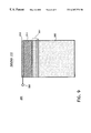
- a memory device 10 includes a substrate 12 having a pad stack 11 formed thereon.
- Substrate 12 is preferably a monocrystalline silicon substrate.
- Pad stack 11 includes an oxide layer 14 and a nitride layer 16 .
- a hard mask layer 18 is deposited on pad stack 11 .
- Hard mask 18 typically includes boron doped silicate glass (BSG).
- BSG boron doped silicate glass
- Hard mask 18 is patterned using lithographic techniques known to those skilled in the art to form holes 15 where deep trenches 17 will be formed. Formation of trench 17 is preferably formed by employing an anisotropic etch, such as a reactive ion etch (RIE).
- RIE reactive ion etch
- Trench 17 is etched into substrate 12 . During this process, however, hard mask 18 is eroded away which may cause collateral damage to areas adjacent to the position of trench 17 . The longer etching occurs, the higher the risk of eroding away hard mask 18 .
- a thicker hard mask 18 may be used. However, this increases process time and does not necessarily provide a deeper trench.
- a method for forming a valve metal oxide for semiconductor fabrication in accordance with the present invention includes the steps of providing a semiconductor wafer, depositing a valve metal material on the wafer, placing the wafer in an electrochemical cell such that a solution including electrolytes interacts with the valve metal material to form a metal oxide when a potential difference is provided between the valve metal material and the solution and processing the wafer using the metal oxide layer.
- a method for etching trenches in a semiconductor substrate includes the steps of providing a semiconductor substrate, forming a pad stack of the substrate, depositing a valve metal material on the pad stack, placing the substrate in an electrochemical cell such that a solution including electrolytes interacts with the valve metal material to form a metal oxide when a potential difference is provided between the valve metal material and the solution, and employing the metal oxide as an etch mask for etching trenches into the substrate.
- Another method for forming a valve metal oxide for semiconductor fabrication includes the steps of providing a semiconductor wafer including a substrate having at least one layer formed thereon, depositing a dielectric layer on the at least one layer, depositing a valve metal material on the dielectric layer, oxidizing the valve metal material by placing the wafer in an electrochemical cell such that a solution including electrolytes interacts with the valve metal material to form a metal oxide when a potential difference is provided between the valve metal material and the solution, the dielectric layer for providing protection for the at least one layer during the oxidizing step, and processing the wafer using the metal oxide layer.
- the step of depositing a valve metal material may include depositing a valve metal material selected from the group consisting of aluminum, niobium, tantalum, titanium, titanium nitride, hafnium and zirconium.
- the method may include the step of applying a voltage between the valve metal material and the solution to create the potential difference such that the voltage applied controls the thickness of the metal oxide.
- the solution may include an acetate buffer in aqueous solution.
- the acetate buffer solution preferably has a pH of between about 4 and about 7.
- the step of placing the wafer in an electrochemical cell may include the steps of placing the wafer in an electrochemical cell such that the wafer has an exposed surface area of valve metal, and providing a counter electrode in the solution having a greater exposed surface area than the exposed surface area of the valve metal.
- the step of placing the wafer in an electrochemical cell may include the step of sealing other than exposed areas of the valve metal material to prevent contact with the solution.
- the solution which includes electrolytes preferably interacts with the valve metal material to form the metal oxide at about room temperature.
- the step of processing the wafer using the metal oxide layer may include the step of employing the metal oxide layer as an etch mask and/or etch stop.
- the step of employing the metal oxide as an etch mask for etching trenches into the substrate may include the step of patterning the valve metal material to open holes at locations for the trenches.
- the step of employing the metal oxide as an etch mask for etching trenches into the substrate may include the step of patterning the metal oxide to open holes at locations for the trenches.
- the step of processing the wafer may include the step of patterning the valve metal material to open holes at locations for trenches to employ the metal oxide as an etch mask.
- the step of processing the wafer may include the step of patterning the metal oxide to open holes at locations for trenches to employ the metal oxide as an etch mask.
- FIG. 1 is a cross-sectional view of a conventional semiconductor device showing erosion of a hard mask during trench etching
- FIG. 2 is a cross-sectional view of a semiconductor device showing a valve metal material layer deposited thereon in accordance with the present invention
- FIG. 3 is a cross-sectional view of the semiconductor device showing the valve metal material layer of FIG. 2 oxidized in accordance with the present invention, after the valve metal material layer is patterned;
- FIG. 4 is a schematic diagram of an apparatus for electrochemically forming a valve metal oxide in accordance with the present invention.
- FIG. 5 is a graph of capacitance C (charge storage) versus potential U for processing in accordance with the present invention
- FIG. 6 is a graph of current I versus potential U for processing in accordance with the present invention.
- FIG. 7 is a cross-sectional view of the semiconductor device of FIG. 3 showing the oxidized valve metal layer functioning as an etch mask in accordance with the present invention
- FIG. 8 is a cross-sectional view of a semiconductor device showing a valve metal material layer deposited on a protective dielectric layer in accordance with the present invention
- FIG. 9 is a cross-sectional view of the semiconductor device showing the valve metal material layer of FIG. 8 oxidized in accordance with the present invention, before the oxidized metal layer is patterned;
- FIG. 10 is a cross-sectional view of the semiconductor device of FIG. 9 showing the oxidized metal layer functioning as an etch mask in accordance with the present invention.
- the present invention relates to semiconductor fabrication and more particularly, to hard masks having improved selective etching capabilities.
- the hard masks in accordance with the present invention include metals, such as valve metals or other conductive compounds such as titanium nitride (TiN).
- valve metals will be considered to include theses other compounds as well.
- the valve metals are preferably oxidized by a low temperature oxidation method.
- valve metal oxides such as Al 2 O 3 , TiO 2 , Ta 2 O 5 , Nb 2 O 6 , ZrO 2 and HfO 2 are employed. These oxides show high etch selectivity and may be formed by a more economically efficient method than prior art hard masks.
- a process for the formation of valve metal oxide hard masks at low temperature will now be described in greater detail.
- a semiconductor device 100 may include a memory device, such as, a dynamic random access memory (DRAM), synchronous DRAM, static RAMs, and read only memories or other memory integrated circuits.
- Device 100 may also include processor chips, logic circuits, application specific chips or the like.
- Device 100 and the following method will be illustratively described for the formation of deep trenches in semiconductor memories, however the invention is much broader and is applicable to any semiconductor device employing an etch mask or a layer of valve metal oxides for any process step.
- Device 100 includes a substrate 102 .
- Substrate 102 which may include a silicon material, although of substrate materials may be employed, for example, gallium arsenide, silicon-on-insulator, etc.
- a pad stack 101 is formed on a top surface 104 of substrate 102 .
- Pad stack 101 may include an oxide layer 106 and a nitride layer 108 . Other layers may be provided or multiple oxides and/or nitride layers may be employed.
- Valve metal layer 110 is deposited on pad stack 101 .
- Valve metal layer 110 may include one or more of aluminum (Al), titanium (Ti), tantalum (Ta), niobium (Nb), zirconium (Zr) and/or hafnium (Hf).
- Other conductive metal valve compounds may be used which form an oxide which is selectively etchable relative to substrate 102 , for example TiN may be used.
- Valve metal layer 110 may be deposited using a chemical vapor deposition (CVD) process. Alternately, valve metal layer 110 may be deposited using a physical vapor deposition (PVD) process.
- Valve metal layer 110 may be deposited to a thickness of between about 10 nm and about 600 nm, preferably between about 100 nm and about 300 nm, although other thicknesses may be used.
- Valve metal layer 110 may be patterned at this point or oxidized and then patterned. In either case, the oxide or metal is removed in accordance with a lithographic pattern and by lithography techniques known to those skilled in the art. For convenience, the case where valve metal layer 110 is patterned prior to oxidation is shown in FIG. 3 . Patterning valve metal layer 110 prior to oxidation is preferred since layer 110 can be selectively etched relative to a lithographic resist layer.
- the resist layer (not shown) has a selectivity to layer 110 which is sufficient to open layer 110 having a thickness of about 600 nm, using a reactive ion etch (RIE). Other layer thicknesses may be used as well. This corresponds to a hard mask open process. By patterning layer 110 in this way, layer 110 is easily patterned due to the selectivity of the metal layer to the resist. The resist layer is then removed.
- RIE reactive ion etch
- valve metal layer 110 is now oxidized by a low temperature oxidation process in accordance with the invention to form a metal oxide layer 120 (FIG. 7 ).
- An electrode 112 is connected to valve metal layer 110 (or alternately substrate 102 if an appropriate conductive path exists between substrate 102 and valve metal 110 ), and device 100 is exposed to an electrolyte solution 114 .
- Valve metals and their compounds may be oxidized anodically, in accordance with the invention, to form uniform oxide films.
- valve metal oxide electrochemical reaction permits current flow in one direction only, i.e. toward oxide formation.
- a stationary film thickness d is determined by an applied potential U according to a high field model as:
- Valve metal layer 110 is oxidized at about room temperature although other temperatures may be employed to achieve different results.
- the oxidation process is well controlled and results in uniform oxidation.
- the controlled oxidation can be achieved with the apparatus shown in FIG. 4 .
- the process converts metals and metal compounds (TiN) to oxides. Theses oxides are now useful as hardmasks since they provide exceptional resistance to reactive ion etching processes which follow.
- Apparatus 200 is an electrochemical cell which includes a bath 204 which is filled with a liquid 206 including an electrolyte.
- Liquid 206 is preferably water and the electrolyte may include ionic compounds such as salts, acid compounds, base compounds, etc. or a combination thereof.
- the electrolyte includes an acetic buffer having a pH concentration of between about 4 and about 7. Other compounds and concentrations are contemplated and may be provided such that ions are capable of transfer between electrodes in bath 204 .
- Device 100 which is preferably included on semiconductor wafer 202 , is secured to an isolating wafer holder 210 .
- Clamps 212 are provided about a periphery of wafer 202 to both secure and seal wafer 202 such that only an upper face 214 of device 100 is exposed to solution 206 in bath 204 .
- Electrical contact is made to device 100 on a backside 216 through a conductive wire 218 or to valve metal layer 110 directly, if insulating layers exist between substrate 102 and valve metal layer 110 , such as in the case described above.
- a conductive film or foil 220 may be disposed between a non-conductive or isolating wafer holder 210 and wafer 202 to improve electrical contact between wire 218 and wafer 202 .
- a reference electrode 222 is included in bath 204 to maintain a predefined potential in solution 206 (also labeled as solution 114 in FIGS. 3 and 9 ). Reference electrode 222 maintains a defined potential on device 100 , which preferably is a chip or wafer.
- a counter electrode 224 is also included. Counter electrode 224 preferably includes at least the same amount of exposed surface area as device 100 . Preferably, counter electrode 224 is large versus the surface of device 100 . That is, the surface area of counter electrode 224 is about 1.5 to about 50 times the surface area of valve metal layer 110 .
- Counter electrode 224 preferably includes a noble metal (such as, gold (Au) or platinum (Pt)) or, to minimize contamination concerns, counter electrode 224 preferably includes the same metal that has to be oxidized on the wafer, i.e., the metal of valve metal layer 110 .
- a noble metal such as, gold (Au) or platinum (Pt)
- counter electrode 224 preferably includes the same metal that has to be oxidized on the wafer, i.e., the metal of valve metal layer 110 .
- the optimum conditions for the electrolyte will depend on the respective valve metal.
- a voltage source or potentiostat 226 is included for providing a voltage difference between device 100 and reference electrode 222 .
- This voltage difference is used to control the thickness of oxide formed on device 100 as described above.
- the wafer with device 100 needs to be immersed into electrolyte solution 206 .
- the potential is gradually raised to a target potential, which is needed for the desired film thickness and maintained at that potential for a defined period of time.
- the oxidation current and thus the charge can be monitored in-situ. When a particular value of the total charge has been transferred, the oxidation is complete.
- the quantities of charge needed to establish a given oxide thickness depends on the metal used.
- valve metals for example, Al, Ta, Nb, Hf, Ti and Zr in an electrolyte solution, such as, an acetate buffer with a pH of 5.9.
- an electrolyte solution such as, an acetate buffer with a pH of 5.9.
- FIG. 6 shows a current I caused by potential U.
- FIG. 5 shows capacitance C versus potential U.
- properties of the metal oxide layer may be determined, for example, oxide layer thickness, lateral expansion of the metal oxide layer, etc.
- this information may eliminate the need for making physical measurements of the metal oxide layer formed in accordance with the invention.
- etching substrate 102 is now performed using a valve metal oxide layer 120 .
- Layer 120 provides high etch resistance and high etch selectivity to silicon (substrate 102 ) so that a trench 122 may be formed.
- Valve metal oxide layer 120 may preferably include, Al 2 O 3 , TiO 2 , Ta 2 O 5 , Nb 2 O 6 , ZrO 2 and HfO 2 . Other oxides may be formed in accordance with the invention as well.
- the high etch resistance and high etch selectivity of the valve metal oxide layer 120 provides a longer etch time for reactive ion etching (or other etching process). In the illustrative example involving deep trench formation, the longer etch time provides the capability of etching deeper trenches without the concern for erosion. Processing may now continue as is known in the art.
- an alternate embodiment includes a device 300 which includes a substrate 302 .
- Substrate 302 which may include a silicon material, although of substrate materials may be employed.
- a pad stack 301 is formed on a top surface 304 of substrate 302 .
- Pad stack 301 may include an oxide layer 306 and a nitride layer 308 . Other layers may be provided or multiple oxide and/or nitride layers may be employed.
- a dielectric layer 311 may be deposited over pad stack 301 .
- Dielectric layer 301 may include an oxide, such as boron silicate glass (BSG) or other material which is selectively removable relative to the top layer of pad stack 301 .
- BSG boron silicate glass
- Dielectric layer 311 is provided to protect pad stack 301 or other components of device 300 during anodic oxidation in later steps.
- Dielectric layer 311 includes a thickness sufficient to prevent over oxidation.
- a valve metal layer 310 is deposited on dielectric layer 311 .
- Valve metal layer 310 may be deposited using a chemical vapor deposition (CVD) process or a physical vapor deposition (PVD) process as described above.
- CVD chemical vapor deposition
- PVD physical vapor deposition
- Valve metal layer 310 may be patterned at this point or oxidized and then patterned. In either case, the oxide or metal is removed in accordance with a lithographic pattern and by lithography techniques known to those skilled in the art. The case where the valve metal layer 310 is patterned after oxidation is shown in FIG. 9 .
- layer 310 is oxidized by a low temperature oxidation process as described above with reference to FIG. 4 .
- An electrode 320 is connected to valve metal layer 310 or to substrate 302 .
- Valve metal layer 310 may be permitted to make contact to substrate 302 in some locations, thereby permitting electrode 320 to be connected to substrate 302 .
- Layer 310 is completely oxidized to form a layer 322 (FIG. 10) which is a valve metal oxide layer.
- valve metal oxide layer 310 has been patterned using a resist (not shown) as described above.
- Layer 322 may be etched by dry etch process such as a RIE process selective to the resist. Openings 313 are formed through a valve metal oxide layer 322 .
- Etching of trenches 316 is now performed. In accordance with the invention, deeper trenches 316 are capable of being formed since the valve metal oxide provides superior etch resistance to RIE. Processing may now continue as is known in the art.
- the present provides a method for forming hardmasks without expending thermal budget.
- the present invention forms the oxide compounds at about room temperature.
- the thermal formation of these valve metal oxide films would normally require working at fairly high temperatures of several hundred degrees Celsius.
- Valve metal oxide layers may be removed using a wet etch process, for example.
- the present invention provides a uniform and dense (pin hole free) valve metal oxide film on a wafer by anodic oxidation of the respective metal films before or after structuring.
- a valve metal oxide layer may be formed as a mask for dopant implantation or as a stop layer for etching or polishing.
Landscapes
- Engineering & Computer Science (AREA)
- Physics & Mathematics (AREA)
- Condensed Matter Physics & Semiconductors (AREA)
- General Physics & Mathematics (AREA)
- Manufacturing & Machinery (AREA)
- Computer Hardware Design (AREA)
- Microelectronics & Electronic Packaging (AREA)
- Power Engineering (AREA)
- Chemical & Material Sciences (AREA)
- Inorganic Chemistry (AREA)
- Chemical Kinetics & Catalysis (AREA)
- Electrochemistry (AREA)
- Materials Engineering (AREA)
- Metallurgy (AREA)
- Organic Chemistry (AREA)
- Semiconductor Memories (AREA)
- Weting (AREA)
- Formation Of Insulating Films (AREA)
Priority Applications (7)
| Application Number | Priority Date | Filing Date | Title |
|---|---|---|---|
| US09/327,711 US6387771B1 (en) | 1999-06-08 | 1999-06-08 | Low temperature oxidation of conductive layers for semiconductor fabrication |
| EP00937744A EP1186015A1 (en) | 1999-06-08 | 2000-05-25 | Low temperature oxidation of conductive layers for semiconductor fabrication |
| PCT/US2000/014343 WO2000075978A1 (en) | 1999-06-08 | 2000-05-25 | Low temperature oxidation of conductive layers for semiconductor fabrication |
| JP2001502156A JP2003501831A (ja) | 1999-06-08 | 2000-05-25 | 半導体製造のために導電性層を低温酸化する方法 |
| CN00808743A CN1355930A (zh) | 1999-06-08 | 2000-05-25 | 用于半导体制造的导电层的低温氧化 |
| KR1020017015317A KR20020010679A (ko) | 1999-06-08 | 2000-05-25 | 반도체 제조를 위한 전도층의 저온 산화물 형성 방법 |
| TW089111040A TW519705B (en) | 1999-06-08 | 2000-06-27 | Low temperature oxidation of conductive layers for semiconductor fabrication |
Applications Claiming Priority (1)
| Application Number | Priority Date | Filing Date | Title |
|---|---|---|---|
| US09/327,711 US6387771B1 (en) | 1999-06-08 | 1999-06-08 | Low temperature oxidation of conductive layers for semiconductor fabrication |
Publications (1)
| Publication Number | Publication Date |
|---|---|
| US6387771B1 true US6387771B1 (en) | 2002-05-14 |
Family
ID=23277714
Family Applications (1)
| Application Number | Title | Priority Date | Filing Date |
|---|---|---|---|
| US09/327,711 Expired - Lifetime US6387771B1 (en) | 1999-06-08 | 1999-06-08 | Low temperature oxidation of conductive layers for semiconductor fabrication |
Country Status (7)
| Country | Link |
|---|---|
| US (1) | US6387771B1 (zh) |
| EP (1) | EP1186015A1 (zh) |
| JP (1) | JP2003501831A (zh) |
| KR (1) | KR20020010679A (zh) |
| CN (1) | CN1355930A (zh) |
| TW (1) | TW519705B (zh) |
| WO (1) | WO2000075978A1 (zh) |
Cited By (7)
| Publication number | Priority date | Publication date | Assignee | Title |
|---|---|---|---|---|
| US20040129960A1 (en) * | 2002-12-27 | 2004-07-08 | Junya Maruyama | Semiconductor device and manufacturing method thereof, delamination method, and transferring method |
| US20050176256A1 (en) * | 2004-02-10 | 2005-08-11 | Infineon Technologies Ag | Method for expanding a trench in a semiconductor structure |
| US20050255581A1 (en) * | 2002-08-28 | 2005-11-17 | University Of Pittsburgh | Self-organized nanopore arrays with controlled symmetry and order |
| US20080006810A1 (en) * | 2006-07-06 | 2008-01-10 | Chanro Park | Memory structure and method of manufacture |
| US20080241996A1 (en) * | 2006-09-29 | 2008-10-02 | Shinobu Fujita | Manufacturing method of semiconductor device |
| US20100078618A1 (en) * | 2008-09-30 | 2010-04-01 | Sandisk 3D Llc | Self-assembly process for memory array |
| US20100101457A1 (en) * | 2007-05-25 | 2010-04-29 | Surace Kevin J | Low embodied energy sheathing panels and methods of making same |
Families Citing this family (2)
| Publication number | Priority date | Publication date | Assignee | Title |
|---|---|---|---|---|
| JP4384387B2 (ja) | 2002-02-20 | 2009-12-16 | ティアック株式会社 | 光ディスク装置 |
| US11427921B2 (en) * | 2017-02-01 | 2022-08-30 | Tokyo Electron Limited | Electrolytic treatment apparatus and electrolytic treatment method |
Citations (13)
| Publication number | Priority date | Publication date | Assignee | Title |
|---|---|---|---|---|
| US3634203A (en) * | 1969-07-22 | 1972-01-11 | Texas Instruments Inc | Thin film metallization processes for microcircuits |
| US3971710A (en) * | 1974-11-29 | 1976-07-27 | Ibm | Anodized articles and process of preparing same |
| DE2746225A1 (de) | 1977-09-14 | 1979-03-22 | Bbc Brown Boveri & Cie | Verfahren zur herstellung von lokalen anodischen oxidschichten |
| US4146440A (en) * | 1978-04-03 | 1979-03-27 | Burroughs Corporation | Method for forming an aluminum interconnect structure on an integrated circuit chip |
| US4242791A (en) * | 1979-09-21 | 1981-01-06 | International Business Machines Corporation | High performance bipolar transistors fabricated by post emitter base implantation process |
| US4261792A (en) * | 1976-05-11 | 1981-04-14 | Matsushita Electric Industrial Co., Ltd. | Method for fabrication of semiconductor devices |
| JPS5994438A (ja) | 1982-11-19 | 1984-05-31 | Tdk Corp | パタ−ン化されたアルミニウム層を形成する方法 |
| US4502204A (en) * | 1981-07-17 | 1985-03-05 | Citizen Watch Company Limited | Method of manufacturing insulated gate thin film field effect transistors |
| US4624048A (en) * | 1983-08-17 | 1986-11-25 | International Business Machines | Method of making magnetic head sliders |
| US4648937A (en) * | 1985-10-30 | 1987-03-10 | International Business Machines Corporation | Method of preventing asymmetric etching of lines in sub-micrometer range sidewall images transfer |
| US5549931A (en) | 1995-02-27 | 1996-08-27 | Council Of Scientific & Industrial Research | Process for the preparation of uniform ultra thin films of metal oxide, metal chalco-genides and metal halides |
| DE19728473A1 (de) | 1997-07-03 | 1999-01-07 | Siemens Ag | Strukturierungsverfahren |
| US6030517A (en) * | 1995-04-06 | 2000-02-29 | Centre National De La Recherche Scientifique | Process for preparing a film of an oxide or a hydroxide of an element of groups IIB or IIIA of the periodic table, and the composite structures which include such a film |
-
1999
- 1999-06-08 US US09/327,711 patent/US6387771B1/en not_active Expired - Lifetime
-
2000
- 2000-05-25 WO PCT/US2000/014343 patent/WO2000075978A1/en not_active Application Discontinuation
- 2000-05-25 KR KR1020017015317A patent/KR20020010679A/ko not_active Application Discontinuation
- 2000-05-25 EP EP00937744A patent/EP1186015A1/en not_active Withdrawn
- 2000-05-25 JP JP2001502156A patent/JP2003501831A/ja active Pending
- 2000-05-25 CN CN00808743A patent/CN1355930A/zh active Pending
- 2000-06-27 TW TW089111040A patent/TW519705B/zh active
Patent Citations (13)
| Publication number | Priority date | Publication date | Assignee | Title |
|---|---|---|---|---|
| US3634203A (en) * | 1969-07-22 | 1972-01-11 | Texas Instruments Inc | Thin film metallization processes for microcircuits |
| US3971710A (en) * | 1974-11-29 | 1976-07-27 | Ibm | Anodized articles and process of preparing same |
| US4261792A (en) * | 1976-05-11 | 1981-04-14 | Matsushita Electric Industrial Co., Ltd. | Method for fabrication of semiconductor devices |
| DE2746225A1 (de) | 1977-09-14 | 1979-03-22 | Bbc Brown Boveri & Cie | Verfahren zur herstellung von lokalen anodischen oxidschichten |
| US4146440A (en) * | 1978-04-03 | 1979-03-27 | Burroughs Corporation | Method for forming an aluminum interconnect structure on an integrated circuit chip |
| US4242791A (en) * | 1979-09-21 | 1981-01-06 | International Business Machines Corporation | High performance bipolar transistors fabricated by post emitter base implantation process |
| US4502204A (en) * | 1981-07-17 | 1985-03-05 | Citizen Watch Company Limited | Method of manufacturing insulated gate thin film field effect transistors |
| JPS5994438A (ja) | 1982-11-19 | 1984-05-31 | Tdk Corp | パタ−ン化されたアルミニウム層を形成する方法 |
| US4624048A (en) * | 1983-08-17 | 1986-11-25 | International Business Machines | Method of making magnetic head sliders |
| US4648937A (en) * | 1985-10-30 | 1987-03-10 | International Business Machines Corporation | Method of preventing asymmetric etching of lines in sub-micrometer range sidewall images transfer |
| US5549931A (en) | 1995-02-27 | 1996-08-27 | Council Of Scientific & Industrial Research | Process for the preparation of uniform ultra thin films of metal oxide, metal chalco-genides and metal halides |
| US6030517A (en) * | 1995-04-06 | 2000-02-29 | Centre National De La Recherche Scientifique | Process for preparing a film of an oxide or a hydroxide of an element of groups IIB or IIIA of the periodic table, and the composite structures which include such a film |
| DE19728473A1 (de) | 1997-07-03 | 1999-01-07 | Siemens Ag | Strukturierungsverfahren |
Cited By (18)
| Publication number | Priority date | Publication date | Assignee | Title |
|---|---|---|---|---|
| US20050255581A1 (en) * | 2002-08-28 | 2005-11-17 | University Of Pittsburgh | Self-organized nanopore arrays with controlled symmetry and order |
| US7723209B2 (en) | 2002-12-27 | 2010-05-25 | Semiconductor Energy Laboratory Co., Ltd. | Semiconductor device and manufacturing method thereof, delamination method, and transferring method |
| US8691604B2 (en) | 2002-12-27 | 2014-04-08 | Semiconductor Energy Laboratory Co., Ltd. | Semiconductor device and manufacturing method thereof, delamination method, and transferring method |
| US9269817B2 (en) | 2002-12-27 | 2016-02-23 | Semiconductor Energy Laboratory Co., Ltd. | Semiconductor device and manufacturing method thereof, delamination method, and transferring method |
| US8247246B2 (en) | 2002-12-27 | 2012-08-21 | Semiconductor Energy Laboratory Co., Ltd. | Semiconductor device and manufacturing method thereof, delamination method, and transferring method |
| US9543337B2 (en) | 2002-12-27 | 2017-01-10 | Semiconductor Energy Laboratory Co., Ltd. | Semiconductor device and manufacturing method thereof, delamination method, and transferring method |
| US20100248402A1 (en) * | 2002-12-27 | 2010-09-30 | Semiconductor Energy Laboratory Co., Ltd. | Semiconductor device and manufacturing method thereof, delamination method, and transferring method |
| US10038012B2 (en) | 2002-12-27 | 2018-07-31 | Semiconductor Energy Laboratory Co., Ltd. | Semiconductor device and manufacturing method thereof, delamination method, and transferring method |
| US20040129960A1 (en) * | 2002-12-27 | 2004-07-08 | Junya Maruyama | Semiconductor device and manufacturing method thereof, delamination method, and transferring method |
| US7157382B2 (en) * | 2004-02-10 | 2007-01-02 | Infineon Technologies Ag | Method for expanding a trench in a semiconductor structure |
| US20050176256A1 (en) * | 2004-02-10 | 2005-08-11 | Infineon Technologies Ag | Method for expanding a trench in a semiconductor structure |
| US7423282B2 (en) * | 2006-07-06 | 2008-09-09 | Infineon Technologies Ag | Memory structure and method of manufacture |
| US20080006810A1 (en) * | 2006-07-06 | 2008-01-10 | Chanro Park | Memory structure and method of manufacture |
| US7772035B2 (en) * | 2006-09-29 | 2010-08-10 | Kabushiki Kaisha Toshiba | Manufacturing method of semiconductor device |
| US20080241996A1 (en) * | 2006-09-29 | 2008-10-02 | Shinobu Fujita | Manufacturing method of semiconductor device |
| US20100101457A1 (en) * | 2007-05-25 | 2010-04-29 | Surace Kevin J | Low embodied energy sheathing panels and methods of making same |
| US8008213B2 (en) | 2008-09-30 | 2011-08-30 | Sandisk 3D Llc | Self-assembly process for memory array |
| US20100078618A1 (en) * | 2008-09-30 | 2010-04-01 | Sandisk 3D Llc | Self-assembly process for memory array |
Also Published As
| Publication number | Publication date |
|---|---|
| TW519705B (en) | 2003-02-01 |
| KR20020010679A (ko) | 2002-02-04 |
| CN1355930A (zh) | 2002-06-26 |
| JP2003501831A (ja) | 2003-01-14 |
| EP1186015A1 (en) | 2002-03-13 |
| WO2000075978A1 (en) | 2000-12-14 |
Similar Documents
| Publication | Publication Date | Title |
|---|---|---|
| US7566939B2 (en) | Fabrication of silicon micro-mechanical structures | |
| KR100689916B1 (ko) | 반도체 집적 회로 장치의 제조 방법 | |
| JPH0793363B2 (ja) | 半導体集積回路およびその作製方法 | |
| US6387771B1 (en) | Low temperature oxidation of conductive layers for semiconductor fabrication | |
| KR100199346B1 (ko) | 반도체 소자의 전하저장전극 형성방법 | |
| US6559069B2 (en) | Process for the electrochemical oxidation of a semiconductor substrate | |
| US20050245025A1 (en) | Method of fabricating bottle trench capacitors using an electrochemical etch with electrochemical etch stop | |
| US7259061B2 (en) | Method for forming a capacitor for an integrated circuit and integrated circuit | |
| EP1183721B1 (en) | Low temperature sacrificial oxide formation | |
| Michaelis | Valve metal, Si and ceramic oxides as dielectric films for passive and active electronic devices | |
| WO2001015221A1 (en) | Selective oxide etch for forming a protection layer with different oxide thicknesses | |
| KR20000074605A (ko) | 반도체 소자 제조방법 | |
| Szwarc et al. | Modelling of the electrochemical etch stop with high reverse bias across pn-junctions | |
| KR100318436B1 (ko) | 반도체 소자의 폴리사이드 전극 형성방법 | |
| JP3437387B2 (ja) | 半導体装置 | |
| KR100324330B1 (ko) | 반도체소자의 콘택 형성방법 | |
| TW380300B (en) | Employing thin multilayer polysilicon to reduce the depth of buried layer trench | |
| KR20090022802A (ko) | 반도체 소자의 제조방법 | |
| KR20040001947A (ko) | 반도체 제조방법 | |
| KR20020056635A (ko) | 반도체 소자의 커패시터 형성 방법 | |
| KR20020045886A (ko) | 반도체소자의 캐패시터 형성방법 |
Legal Events
| Date | Code | Title | Description |
|---|---|---|---|
| AS | Assignment |
Owner name: INFINEON TECHNOLOGIES CORPORATION, CALIFORNIA Free format text: ASSIGNMENT OF ASSIGNORS INTEREST;ASSIGNORS:GENZ, OLIVER;MICHAELIS, ALEXANDER;REEL/FRAME:010032/0436 Effective date: 19990528 |
|
| AS | Assignment |
Owner name: INFINEON TECHNOLOGIES NORTH AMERICA CORP., CALIFOR Free format text: CHANGE OF NAME;ASSIGNOR:INFINEON TECHNOLOGIES CORPORATION;REEL/FRAME:011174/0136 Effective date: 19990930 |
|
| AS | Assignment |
Owner name: INFINEON TECHNOLOGIES AG, GERMANY Free format text: ASSIGNMENT OF ASSIGNORS INTEREST;ASSIGNOR:INFINEON TECHNOLOGIES NORTH AMERICA CORP.;REEL/FRAME:012465/0271 Effective date: 20011107 |
|
| STCF | Information on status: patent grant |
Free format text: PATENTED CASE |
|
| FPAY | Fee payment |
Year of fee payment: 4 |
|
| FPAY | Fee payment |
Year of fee payment: 8 |
|
| AS | Assignment |
Owner name: QIMONDA AG, GERMANY Free format text: ASSIGNMENT OF ASSIGNORS INTEREST;ASSIGNOR:INFINEON TECHNOLOGIES AG;REEL/FRAME:023773/0001 Effective date: 20060425 Owner name: QIMONDA AG,GERMANY Free format text: ASSIGNMENT OF ASSIGNORS INTEREST;ASSIGNOR:INFINEON TECHNOLOGIES AG;REEL/FRAME:023773/0001 Effective date: 20060425 |
|
| FPAY | Fee payment |
Year of fee payment: 12 |
|
| AS | Assignment |
Owner name: INFINEON TECHNOLOGIES AG, GERMANY Free format text: ASSIGNMENT OF ASSIGNORS INTEREST;ASSIGNOR:QIMONDA AG;REEL/FRAME:035623/0001 Effective date: 20141009 |
|
| AS | Assignment |
Owner name: POLARIS INNOVATIONS LIMITED, IRELAND Free format text: ASSIGNMENT OF ASSIGNORS INTEREST;ASSIGNOR:INFINEON TECHNOLOGIES AG;REEL/FRAME:036539/0196 Effective date: 20150708 |