US6317005B1 - Process of clock recovery during the sampling of digital-type signals - Google Patents
Process of clock recovery during the sampling of digital-type signals Download PDFInfo
- Publication number
- US6317005B1 US6317005B1 US09/295,502 US29550299A US6317005B1 US 6317005 B1 US6317005 B1 US 6317005B1 US 29550299 A US29550299 A US 29550299A US 6317005 B1 US6317005 B1 US 6317005B1
- Authority
- US
- United States
- Prior art keywords
- process according
- value
- phase
- digital
- sampling
- Prior art date
- Legal status (The legal status is an assumption and is not a legal conclusion. Google has not performed a legal analysis and makes no representation as to the accuracy of the status listed.)
- Expired - Lifetime
Links
Images


Classifications
-
- G—PHYSICS
- G09—EDUCATION; CRYPTOGRAPHY; DISPLAY; ADVERTISING; SEALS
- G09G—ARRANGEMENTS OR CIRCUITS FOR CONTROL OF INDICATING DEVICES USING STATIC MEANS TO PRESENT VARIABLE INFORMATION
- G09G5/00—Control arrangements or circuits for visual indicators common to cathode-ray tube indicators and other visual indicators
- G09G5/003—Details of a display terminal, the details relating to the control arrangement of the display terminal and to the interfaces thereto
- G09G5/006—Details of the interface to the display terminal
- G09G5/008—Clock recovery
-
- H—ELECTRICITY
- H04—ELECTRIC COMMUNICATION TECHNIQUE
- H04L—TRANSMISSION OF DIGITAL INFORMATION, e.g. TELEGRAPHIC COMMUNICATION
- H04L7/00—Arrangements for synchronising receiver with transmitter
- H04L7/02—Speed or phase control by the received code signals, the signals containing no special synchronisation information
- H04L7/033—Speed or phase control by the received code signals, the signals containing no special synchronisation information using the transitions of the received signal to control the phase of the synchronising-signal-generating means, e.g. using a phase-locked loop
-
- H—ELECTRICITY
- H04—ELECTRIC COMMUNICATION TECHNIQUE
- H04N—PICTORIAL COMMUNICATION, e.g. TELEVISION
- H04N5/00—Details of television systems
- H04N5/04—Synchronising
- H04N5/12—Devices in which the synchronising signals are only operative if a phase difference occurs between synchronising and synchronised scanning devices, e.g. flywheel synchronising
- H04N5/126—Devices in which the synchronising signals are only operative if a phase difference occurs between synchronising and synchronised scanning devices, e.g. flywheel synchronising whereby the synchronisation signal indirectly commands a frequency generator
Definitions
- the present invention relates to a process of clock recovery during the sampling of digital-type signals, more especially a process making it possible to recover the clock during the sampling of video signals emanating from a computer device.
- the sampling of video signals emanating from an analog source is well known. It uses the Shannon-Nyquist theorem. According to this theorem, if the passband of a signal is limited to a frequency range such as [0,Fmax], it is necessary and sufficient to sample this signal at a minimum frequency 2 ⁇ Fmax in order to be capable of reconstructing it from these samples. This constraint is manifested by the introduction of low-pass filters whose purpose is to limit the spectrum of the signals before sampling. In this case, the phase of the clock signal is of no importance in the sampling procedure. Indeed, the same signal sampled by two clocks of the same frequency but which are out of phase contains the same information to within a constant lag.
- the inbound signal is filtered so as to limit its passband and satisfy the Nyquist criteria, the response of the filter to digital-type signals exhibiting steep transitions will engender overoscillations which are very prejudicial to the sharpness of the characters.
- the attenuation afforded to the frequency components will be insufficient to avoid a likewise prejudicial spectral aliasing.
- the purpose of the present invention is to propose a process making it possible automatically to recover the frequency parameter and phase parameter of the sampling clock in the case of the sampling of digital-type signals, more especially of video signals emanating from a computer-type device.
- the subject of the present invention is a process of clock recovery during the sampling of computer-type signals, the sampling clock being generated from a phase locked loop or PLL which multiples a given frequency by an integer number or “division rank”, characterized in that it comprises the following steps:
- the gauging of the position of the edges of the digital-type signals is preceded by an operation of reshaping the said transitions.
- This reshaping is carried out by filtering the digital-type signals with the aid of a high-pass filter and by comparing the amplitude of the filtered signals with a voltage threshold.
- the comparison is carried out by a voltage comparator with hysteresis and the gauging of the position of the edges is carried out by applying the analog ramp to an analog/digital converter whose clock signal is the sampling clock.
- the values corresponding to an absence of utilizable transition and the values corresponding to an overly old transition, namely one prior to the current sampling period are set to the reference value.
- the values used are applied to a circuit making it possible to eliminate the zero values corresponding either to a zero phase error, or to an absence of rising transition, or to an absence of falling transition.
- an initial division rank is calculated as a function of the standard to which the digital-type signals to be sampled belong. This prior calculation makes it possible to accelerate the convergence during correction of the sampling frequency.
- FIG. 1 is a diagrammatic representation of the main circuits used for implementing the present invention.
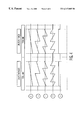
- FIGS. 2A and 2B respectively represent a circuit allowing the detection of the edges and their reshaping as well as the signals applied at various points of the said circuit.
- FIG. 3 diagrammatically represents a circuit for carrying out the phase correction.
- FIGS. 4 and 5 are diagrams illustrating the principle implemented in order to carry out the frequency correction of the sampling clock.
- FIG. 6 diagrammatically represents the circuits used for implementing the frequency correction
- FIGS. 7 and 8 are diagrams in the form of blocks of two embodiments of a phase locked loop making it possible to implement the present invention.
- FIG. 1 A circuit making it possible to implement the process of sampling clock recovery during the sampling of digital-type video signals with a view to a display in accordance with the present invention is represented diagrammatically in FIG. 1 .
- digital-type RGB video signals are amplified by amplifiers 1 . They are sent to analog/digital converters 6 controlled by a sampling clock H which has been processed by the circuit 2 in such a way as to synchronize it with the input signals.
- the circuit 2 comprises an edge extraction circuit 3 , the signal emanating from the circuit 3 is sent to a processor 4 which will output signals shown diagrammatically by the reference S corresponding to a value of division rank and to a phase correction with regard to a PLL 5 which receives as input a line synchronization signal referenced SYNC-H and which outputs the sampling clock H sent to the converters 6 .
- the process of the invention therefore consists in generating the sampling clock H from a PLL which multiplies the inbound line frequency by an integer factor called the division rank. This factor will have to coincide exactly with the total number of pixels of the inbound signal.
- the processor 4 utilizes the position of the transitions of the inbound video which are obtained from the circuit 3 .
- the processor 4 can alter the phase of the sampling clock by detecting the phase variation with the aid of the signals originating from the circuit 3 .
- edge extraction circuit 3 A particular embodiment of the edge extraction circuit 3 will now be described with reference to FIG. 2 .
- the circuit represented in FIG. 2A makes it possible to carry out two operations, namely:
- the digital-type RGB video signals are sent as input to a circuit 30 which carries out analog matricing so as to give a pseudo-luminance signal Y such that
- the signal obtained Y is a staircase function analog type signal such as represented in FIG. 2 B. It comprises pulse-like signals a 1 , a 2 , a 3 exhibiting amplitudes and durations which differ depending on the luminance of the signal.
- the signal Y is applied to a first-order high-pass filter 31 consisting in a known manner of a capacitor C 1 and a resistor Re which is mounted as a differentiator.
- the time constant of the differentiator is chosen, preferably, to be less than the minimum duration of the porch of the inbound signals.
- the signal output by the filter 31 has the shape of the signal b in FIG. 2 B.
- the signal emanating from the high-pass filter is sent to one of the inputs of a comparator 32 whose other input receives a threshold value 34 .
- the comparator 32 is a voltage comparator set up with hysteresis, namely the output from the comparator 32 is looped back to the second input or negative input through an adder 34 .
- the signal applied to the second input of the comparator is represented as c in FIG. 2 B.
- the comparator is quiescent, the signal present at c is a threshold value Sr such that Sr>0.
- the first transition al being less than Sr, there is no a′ 1 represented at d.
- the threshold Sr of the comparator toggles to the working state giving as output a signal such as a′ 2 or a′ 3 in FIG. 2 B.
- this output signal is sent back to the negative input of the comparator 32 where it gets added to the threshold Sr, this modifying the threshold to a value St less than Sr as represented in FIG. 2 B.
- the operation of the comparator is clearly represented by the shape of the signals c, b, d in FIG. 2 B.
- the video transitions of low amplitude are not taken into account by the processor 4 , thus making it possible to render the system insensitive to noise.
- the durations of the high and low porches at the output of the comparator are multiples of the elementary duration of each pixel porch of the inbound video.
- the signals such as those represented at d in FIG. 2B are sent to circuits allowing measurement of the position of the edges.
- These circuits comprise a generator of current I which supplies a circuit composed of a capacitor C 2 and of a switch 33 .
- These two elements make it possible to create the analog ramp which will be applied to the analog/digital converter 34 whose clock is the sampling clock He.
- the circuit described above operates in the following manner. When the comparator is working, the switch 33 is open and the capacitor C 2 charges up. Thus, the voltage across the terminals of the capacitor alters in a linear manner over time giving a voltage ramp. When the comparator goes quiescent, the switch 33 closes and discharges the capacitor C 2 , reinitializing the circuit.
- each new ramp is synchronous with a rising transition in the useful video, as represented at e in FIG. 2 B.
- the signal represented at e is applied to the input of the analog/digital converter 34 whose clock signal is the current sampling clock.
- the choice of the ratio I/C is such that, in one period of the sampling clock, the ramp makes a voltage excursion at least equal to the d.c. input swing of the converter.
- the signals emanating from the converter 34 are sent to the processor 4 making it possible to obtain values for the phase correction and frequency correction of the sampling clock.
- the analog/digital converter gives, for example, 8-bit values which therefore vary between 00 and 255.
- phase correction is carried out by assuming that by convention the sampling phase is optimal when the analog/digital converter 34 which samples the analog ramp emanating from the circuits I and C 2 samples this ramp at its half value, namely 128 in the embodiment represented.
- the phase correction circuit comprises a subtractor 40 which makes it possible to subtract the value 128 from the codes delivered by the converter 34 .
- a signed value of the sampling phase error namely a zero value for an optimal phase, positive for an overly late phase and negative for an overly early phase, is obtained at the output of the subtractor 40 .
- the circuit 40 eliminates the values 00 which correspond to an absence of utilizible signal and the values 255 which correspond to a rising transition prior to a sampling period. To eliminate these values, they replace them by values 128 . Indeed, if a considerable time interval elapses with no falling transition after a rising transition, the ramp remains frozen at its maximum value and the resulting code 255 must not be interpreted as a phase error since it is due merely to the absence of a negative transition engendering the resetting to zero of the ramp.
- the values emanating from the circuit 40 are sent to a circuit which carries out a signed accumulation of the said values.
- This circuit comprises an adder 410 which receives the output signal from the circuit 40 on one input and the output signal from the accumulator 411 on its other input.
- the output from the circuit 411 is also sent as input to a circuit 412 forming an attenuator which retains only the most significant bits so as to carry out the phase correction.
- the signals emanating from the attenuator or truncating circuit 412 are sent to a PWM (Pulse width modulation) converter 413 or a digital/analog converter whose role is to transform the truncated digital output from the accumulator into an analog voltage which will act on the phase of the phase locked loop as will be explained below.
- PWM Pulse width modulation
- FIGS. 4 and 5 illustrate the principle implemented for this frequency correction.
- the principle of the measurement of the position of the edges is such that, depending on the error in the current division rank, consisting of an integer value such as Erg, there exists a linewise periodic phase error function which, for this duration, exhibits a number of maxima which is close to Erg.
- This function can be observed such as represented in FIG. 4 in the particular case of a video template with black and white levels alternating at the pixel frequency.
- the curve a of FIG. 4 represents an error in the division rank of ⁇ 1. In this case, the sampling clock is slower than the pixel clock.
- Curve b represents an error in the division rank of ⁇ 2, in this case the sampling clock is also slower than the pixel clock. It gradually loses its lead up to the first quarter of the line and takes the maximum lag at the middle of the line. This maximum lag abruptly turns into a maximum lead on account of the periodicity of the phase error function.
- the curve c represents an error in the division rank of ⁇ 3 with a sampling clock which is slower than the pixel clock with similar explanations to those given for curve b.
- Curve d relates to an error in the division rank of +4.
- the sampling clock is faster than the pixel clock, it leads up to the 1 ⁇ 8 of the line with a maximum at a quarter of the line. This maximum lead turns into a maximum lag on account of the periodicity of the phase error function.
- Curve e relates to an error in the current division rank of 0. The case represented corresponds to a constant lag of around half the maximum lag. If a phase error is superimposed on a frequency error, the general shape of the curves is identical to within a shift along the time axis. If this simple case is considered, it is found that the sign of the error can be determined by calculating the difference between two consecutive measurements.
- This difference termed the “slip” is positive in cases a, b, c, negative in case d and zero in case e.
- the level of the stable porch of the difference is proportional to the division rank.
- the discontinuity in the periodic function is manifested by a signed peak which is opposite to the porch but very localized.
- d′ represents the differentiated phase error function in the case of a division rank of +4 and D the integer of the sign of the differentiated phase error function for the same value of the division rank.
- the circuits 42 which allow frequency correction consist primarily of a first circuit 420 for eliminating the zero values since these values which correspond either to a zero phase error, or to the absence of a ramp, or to a saturated ramp, do not make it possible to deduce any division rank error.
- This first stage 420 consists of a circuit 420 a for decoding a 0 code, a register RD 420 d and a switch 420 c .
- the output values from the subtractor 40 are therefore copied over as output from the circuit 420 if they are ⁇ 0. In the contrary case, the output from the circuit 420 retains the memory of the last nonzero value delivered by the subtractor 40 .
- the output from the circuit 420 is sent to a circuit for calculating differences 421 .
- This circuit makes it possible to calculate a signed difference between the nonzero values and hence to measure the alteration in the phase error between two consecutive ramps.
- it comprises a register RD 421 a making it possible to store values corresponding to the previous ramp whose output is connected to the minus input of a subtractor 421 b which receives the direct output from the circuit 420 on its plus input.
- the output from the circuit 421 is sent to a thresholding circuit 422 , namely a circuit which makes it possible to calculate only the sign of the value.
- the thresholding is carried out with a dead zone if the slip is very small, so as not to be sensitive to the fluctuations of the analog PLL and carries out a clipping to +1 or ⁇ 1, since the sign of the alteration in the error is sufficient to determine the division rank, the absolute amplitude not being necessary.
- the +1 or ⁇ 1 sign emanating from the circuit 422 is sent to a circuit 423 for accumulating the sign.
- This circuit consists of an adder 423 a which adds the output value from the circuit 422 to the value emanating from a storage circuit 423 b giving the accumulated value.
- the accumulator 423 will be reset to zero by a pulse RZ originating from a thresholding circuit described below.
- the output from the accumulation circuit 423 is sent to a thresholding circuit 424 which receives a threshold pulse Se on an input and transmits, when the threshold which may be positive or negative is exceeded, a reset-to-zero pulse RZ sent back to the circuit 423 as represented in FIG. 6 .
- the thresholding stage 424 then delivers an incremental correction +1 or ⁇ 1 to the next stage, according to whether the threshold crossed is less than 0 or greater than 0.
- This value is accumulated in the accumulation circuit 425 consisting of an adder whose output is looped back to one of the inputs.
- the output value from the adder gives the correction to be applied to the division rank of the PLL.
- an initial division rank is calculated which is added to the correction of the division rank in an adder 426 .
- This initial division rank is obtained by measuring the number of lines per image of the inbound standard. Indeed, since computer standards are characterized only by their active number of pixels and of lines, if the total number of lines is counted, it yields an item of information about the number of active lines and hence it is possible to deduce therefrom an initial estimate of the number of active pixels, based on a statistical analysis of the documentation relating to graphics cards.
- active active total initial pixels lines lines rank VGA 640 480 480 ⁇ nlt ⁇ 600 820 SVGA 800 600 601 ⁇ nlt ⁇ 768 1048 XGA 1024 768 769 ⁇ nlt ⁇ 1024 1320 SXGA 1280 1024 1025 ⁇ nlt 1708
- the division rank obtained is therefore used in a PLL such as represented in FIGS. 7 and 8.
- the PLL of FIG. 7 comprises a phase comparator 50 , an integrator 51 consisting of an amplifier A whose output is looped back to the input by way of a capacitor C 3 in series with a resistor R 3 , the output of the integrator 51 is connected to a voltage-locked oscillator 52 (VCO).
- VCO voltage-locked oscillator
- the output of the VCO is looped back through a circuit 53 giving the division rank in the form of an integer number (:N) on the second input of the phase comparator 50 .
- the first input receives the inbound line sync referenced SYNC-H.
- the value obtained at the output of the circuit 3 can be applied to the terminal 55 and by way of a series resistor R 4 as input to the integrator 51 so as to inject an offset current into the input of the integrator itself linked to the output of the phase comparator by way of a series resistor R 5 .
- a series resistor R 4 By virtue of its almost infinite d.c. gain, the use of an integrator guarantees that the offset current deliberately injected into the output of the comparator will automatically be compensated for by a shift between the sync-H and local H signals such that the mean value of the pulsating current resulting from this shift compensates perfectly for the d.c. offset current injected.
- the phase correction can also be carried out with the aid of a controlled lag formed at the level of the circuit 54 in relation to the line synchronization signal, inbound sync H in a PLL comprising the same elements as the PLL of FIG. 7, namely a phase comparator 50 connected by a series resistor R 5 at the input of an integrator 51 formed of an amplifier looped back by a circuit formed of a capacitor C 3 and of a resistor R 3 in series, the said integrator being connected to a voltage-controlled oscillator 52 , the output of the oscillator being looped back by way of a circuit giving the integer division rank 53 to the local input of the phase comparator 50 , this arrangement being used when all of the above circuits are integrated.
Landscapes
- Engineering & Computer Science (AREA)
- Signal Processing (AREA)
- Physics & Mathematics (AREA)
- Computer Hardware Design (AREA)
- General Physics & Mathematics (AREA)
- Theoretical Computer Science (AREA)
- Computer Networks & Wireless Communication (AREA)
- Multimedia (AREA)
- Stabilization Of Oscillater, Synchronisation, Frequency Synthesizers (AREA)
- Controls And Circuits For Display Device (AREA)
- Analogue/Digital Conversion (AREA)
Applications Claiming Priority (2)
| Application Number | Priority Date | Filing Date | Title |
|---|---|---|---|
| FR9805109A FR2778044B1 (fr) | 1998-04-23 | 1998-04-23 | Procede de recuperation d'horloge lors de l'echantillonnage des signaux de type informatique |
| FR9805109 | 1998-04-23 |
Publications (1)
| Publication Number | Publication Date |
|---|---|
| US6317005B1 true US6317005B1 (en) | 2001-11-13 |
Family
ID=9525600
Family Applications (1)
| Application Number | Title | Priority Date | Filing Date |
|---|---|---|---|
| US09/295,502 Expired - Lifetime US6317005B1 (en) | 1998-04-23 | 1999-04-21 | Process of clock recovery during the sampling of digital-type signals |
Country Status (5)
| Country | Link |
|---|---|
| US (1) | US6317005B1 (de) |
| EP (1) | EP0952568B1 (de) |
| JP (1) | JP4500377B2 (de) |
| DE (1) | DE69934162T2 (de) |
| FR (1) | FR2778044B1 (de) |
Cited By (4)
| Publication number | Priority date | Publication date | Assignee | Title |
|---|---|---|---|---|
| US6750855B1 (en) * | 1999-03-26 | 2004-06-15 | Fujitsu Siemens Computers Gmbh | Method and device for compensating the phase for flat screens |
| US7020227B1 (en) * | 2002-05-31 | 2006-03-28 | Acard Technology Corporation | Method and apparatus for high-speed clock data recovery using low-speed circuits |
| US7719529B2 (en) | 2004-09-28 | 2010-05-18 | Honeywell International Inc. | Phase-tolerant pixel rendering of high-resolution analog video |
| US20120170698A1 (en) * | 2011-01-05 | 2012-07-05 | International Business Machines Corporation | Design structure for window comparator circuit for clock data recovery from bipolar rz data |
Families Citing this family (5)
| Publication number | Priority date | Publication date | Assignee | Title |
|---|---|---|---|---|
| KR100323666B1 (ko) * | 1999-08-12 | 2002-02-07 | 구자홍 | 모니터의 클럭위상 보상장치 및 방법 |
| JP2002196732A (ja) * | 2000-04-27 | 2002-07-12 | Toshiba Corp | 表示装置、画像制御半導体装置、および表示装置の駆動方法 |
| JP3905760B2 (ja) | 2002-01-07 | 2007-04-18 | Necディスプレイソリューションズ株式会社 | 表示装置 |
| GB2385728B (en) * | 2002-02-26 | 2006-07-12 | Fujitsu Ltd | Clock recovery circuitry |
| CN106656182A (zh) * | 2016-11-24 | 2017-05-10 | 深圳市鼎阳科技有限公司 | 一种数字芯片接收adc输出数据的方法及数字芯片 |
Citations (5)
| Publication number | Priority date | Publication date | Assignee | Title |
|---|---|---|---|---|
| EP0519739A1 (de) | 1991-06-19 | 1992-12-23 | Tektronix Inc. | Impulsflanke integrierender Phasendetektor |
| US5297869A (en) * | 1991-02-20 | 1994-03-29 | Research Machines Plc | Apparatus and method for synchronizing a digital data clock in a receiver with a digital data clock in a transmitter |
| EP0660611A2 (de) | 1993-12-23 | 1995-06-28 | Gennum Corporation | Taktrückgewinnungsschaltung für ein serielles digitales Videosignal |
| US5657089A (en) | 1994-10-14 | 1997-08-12 | Nec Corporation | Video signal processing device for sampling TV signals to produce digital data with interval control |
| EP0807923A1 (de) | 1996-05-07 | 1997-11-19 | Matsushita Electric Industrial Co., Ltd. | Verfahren und Vorrichtung zur Wiedergewinnung eines Punkttaktsignales |
Family Cites Families (2)
| Publication number | Priority date | Publication date | Assignee | Title |
|---|---|---|---|---|
| JP3823420B2 (ja) * | 1996-02-22 | 2006-09-20 | セイコーエプソン株式会社 | ドットクロック信号を調整するための方法及び装置 |
| US6226045B1 (en) * | 1997-10-31 | 2001-05-01 | Seagate Technology Llc | Dot clock recovery method and apparatus |
-
1998
- 1998-04-23 FR FR9805109A patent/FR2778044B1/fr not_active Expired - Fee Related
-
1999
- 1999-04-12 DE DE69934162T patent/DE69934162T2/de not_active Expired - Lifetime
- 1999-04-12 EP EP99400884A patent/EP0952568B1/de not_active Expired - Lifetime
- 1999-04-21 JP JP11397399A patent/JP4500377B2/ja not_active Expired - Fee Related
- 1999-04-21 US US09/295,502 patent/US6317005B1/en not_active Expired - Lifetime
Patent Citations (5)
| Publication number | Priority date | Publication date | Assignee | Title |
|---|---|---|---|---|
| US5297869A (en) * | 1991-02-20 | 1994-03-29 | Research Machines Plc | Apparatus and method for synchronizing a digital data clock in a receiver with a digital data clock in a transmitter |
| EP0519739A1 (de) | 1991-06-19 | 1992-12-23 | Tektronix Inc. | Impulsflanke integrierender Phasendetektor |
| EP0660611A2 (de) | 1993-12-23 | 1995-06-28 | Gennum Corporation | Taktrückgewinnungsschaltung für ein serielles digitales Videosignal |
| US5657089A (en) | 1994-10-14 | 1997-08-12 | Nec Corporation | Video signal processing device for sampling TV signals to produce digital data with interval control |
| EP0807923A1 (de) | 1996-05-07 | 1997-11-19 | Matsushita Electric Industrial Co., Ltd. | Verfahren und Vorrichtung zur Wiedergewinnung eines Punkttaktsignales |
Cited By (5)
| Publication number | Priority date | Publication date | Assignee | Title |
|---|---|---|---|---|
| US6750855B1 (en) * | 1999-03-26 | 2004-06-15 | Fujitsu Siemens Computers Gmbh | Method and device for compensating the phase for flat screens |
| US7020227B1 (en) * | 2002-05-31 | 2006-03-28 | Acard Technology Corporation | Method and apparatus for high-speed clock data recovery using low-speed circuits |
| US7719529B2 (en) | 2004-09-28 | 2010-05-18 | Honeywell International Inc. | Phase-tolerant pixel rendering of high-resolution analog video |
| US20120170698A1 (en) * | 2011-01-05 | 2012-07-05 | International Business Machines Corporation | Design structure for window comparator circuit for clock data recovery from bipolar rz data |
| US8477896B2 (en) * | 2011-01-05 | 2013-07-02 | International Business Machines Corporation | Structure for window comparator circuit for clock data recovery from bipolar RZ data |
Also Published As
| Publication number | Publication date |
|---|---|
| DE69934162T2 (de) | 2007-06-06 |
| DE69934162D1 (de) | 2007-01-11 |
| FR2778044A1 (fr) | 1999-10-29 |
| JP4500377B2 (ja) | 2010-07-14 |
| EP0952568B1 (de) | 2006-11-29 |
| FR2778044B1 (fr) | 2000-06-16 |
| EP0952568A1 (de) | 1999-10-27 |
| JP2000056752A (ja) | 2000-02-25 |
Similar Documents
| Publication | Publication Date | Title |
|---|---|---|
| US6636122B2 (en) | Analog frequency locked loop with digital oversampling feedback control and filter | |
| KR100307979B1 (ko) | 보조비디오데이타슬라이서 | |
| US4675724A (en) | Video signal phase and frequency correction using a digital off-tape clock generator | |
| US6317005B1 (en) | Process of clock recovery during the sampling of digital-type signals | |
| US5029004A (en) | Edge enhancement apparatus useful with liquid crystal displays | |
| JP2574038B2 (ja) | 同期サンプリング・システムおよび方法 | |
| US7327399B2 (en) | Method and a circuit for deriving a synchronisation signal from a video signal | |
| EP0378190B1 (de) | Digitale Phasenregelschleife | |
| US6856659B1 (en) | Clock recovery method in digital signal sampling | |
| US5053869A (en) | Digital circuit arrangement detecting synchronizing pulses | |
| EP1100258B1 (de) | Vorrichtung zur Messung der Zeitdauer eines Synchronisierungssignals und Anzeigevorrichtung | |
| JPS58707B2 (ja) | 垂直同期信号検出方法および回路 | |
| US5113257A (en) | Line synchronising circuit | |
| US5767915A (en) | Digital color burst phase switch for pal video systems | |
| US7425993B2 (en) | Video signal processing | |
| US7705917B2 (en) | Method and circuit for extracting synchronization signals in a video signal | |
| JPH11219157A (ja) | サンプリングクロック制御装置 | |
| US5703656A (en) | Digital phase error detector for locking to color subcarrier of video signals | |
| US5270815A (en) | Image compression processing apparatus having means for removing jitter contained at boundary between image and mask portions | |
| JP2874672B2 (ja) | 表示装置における自動位相調整システム | |
| WO1998043439A9 (en) | Video synchronizing signal generator | |
| WO1998043439A1 (en) | Video synchronizing signal generator | |
| JPH11252580A (ja) | ビデオデコーダ及びこれに用いるカラー位相ロックループ | |
| JPS62175073A (ja) | テレビジヨン信号のフレ−ム検出回路 | |
| KR100677073B1 (ko) | 디지털 타이밍 복원장치 |
Legal Events
| Date | Code | Title | Description |
|---|---|---|---|
| AS | Assignment |
Owner name: THOMSON MULTIMEDIA S.A., FRANCE Free format text: ASSIGNMENT OF ASSIGNORS INTEREST;ASSIGNORS:MOREL, PHILIPPE;TAPIE, THIERRY;REEL/FRAME:009926/0871 Effective date: 19990322 |
|
| STCF | Information on status: patent grant |
Free format text: PATENTED CASE |
|
| FPAY | Fee payment |
Year of fee payment: 4 |
|
| FPAY | Fee payment |
Year of fee payment: 8 |
|
| FPAY | Fee payment |
Year of fee payment: 12 |