US6153515A - Method of forming multilayered film - Google Patents
Method of forming multilayered film Download PDFInfo
- Publication number
- US6153515A US6153515A US09/156,896 US15689698A US6153515A US 6153515 A US6153515 A US 6153515A US 15689698 A US15689698 A US 15689698A US 6153515 A US6153515 A US 6153515A
- Authority
- US
- United States
- Prior art keywords
- film
- oxygen
- semiconductor substrate
- nitrided
- nitriding
- Prior art date
- Legal status (The legal status is an assumption and is not a legal conclusion. Google has not performed a legal analysis and makes no representation as to the accuracy of the status listed.)
- Expired - Fee Related
Links
- 238000000034 method Methods 0.000 title claims abstract description 70
- 239000004065 semiconductor Substances 0.000 claims abstract description 67
- 238000005121 nitriding Methods 0.000 claims abstract description 43
- 239000007789 gas Substances 0.000 claims description 93
- 239000000758 substrate Substances 0.000 claims description 70
- 238000000151 deposition Methods 0.000 claims description 55
- 230000008021 deposition Effects 0.000 claims description 55
- QVGXLLKOCUKJST-UHFFFAOYSA-N atomic oxygen Chemical compound [O] QVGXLLKOCUKJST-UHFFFAOYSA-N 0.000 claims description 49
- 239000001301 oxygen Substances 0.000 claims description 49
- 229910052760 oxygen Inorganic materials 0.000 claims description 49
- ATJFFYVFTNAWJD-UHFFFAOYSA-N Tin Chemical compound [Sn] ATJFFYVFTNAWJD-UHFFFAOYSA-N 0.000 claims description 47
- 229910052751 metal Inorganic materials 0.000 claims description 39
- 239000002184 metal Substances 0.000 claims description 39
- 230000003647 oxidation Effects 0.000 claims description 35
- 238000007254 oxidation reaction Methods 0.000 claims description 35
- 238000005229 chemical vapour deposition Methods 0.000 claims description 18
- 150000004767 nitrides Chemical class 0.000 claims description 16
- GWEVSGVZZGPLCZ-UHFFFAOYSA-N Titan oxide Chemical compound O=[Ti]=O GWEVSGVZZGPLCZ-UHFFFAOYSA-N 0.000 claims description 15
- 230000004888 barrier function Effects 0.000 claims description 13
- 239000000203 mixture Substances 0.000 claims description 10
- 229910001080 W alloy Inorganic materials 0.000 claims description 6
- 229910052782 aluminium Inorganic materials 0.000 claims description 5
- 239000012159 carrier gas Substances 0.000 claims description 4
- 229910000838 Al alloy Inorganic materials 0.000 claims description 3
- 229910052721 tungsten Inorganic materials 0.000 claims description 2
- 239000003870 refractory metal Substances 0.000 claims 4
- 150000002927 oxygen compounds Chemical class 0.000 claims 3
- 239000010936 titanium Substances 0.000 abstract description 98
- RTAQQCXQSZGOHL-UHFFFAOYSA-N Titanium Chemical compound [Ti] RTAQQCXQSZGOHL-UHFFFAOYSA-N 0.000 abstract description 19
- 229910052719 titanium Inorganic materials 0.000 abstract description 19
- NRTOMJZYCJJWKI-UHFFFAOYSA-N Titanium nitride Chemical compound [Ti]#N NRTOMJZYCJJWKI-UHFFFAOYSA-N 0.000 abstract description 5
- 230000001590 oxidative effect Effects 0.000 abstract description 5
- 229910003074 TiCl4 Inorganic materials 0.000 description 13
- 230000008569 process Effects 0.000 description 13
- XJDNKRIXUMDJCW-UHFFFAOYSA-J titanium tetrachloride Chemical compound Cl[Ti](Cl)(Cl)Cl XJDNKRIXUMDJCW-UHFFFAOYSA-J 0.000 description 13
- 230000015572 biosynthetic process Effects 0.000 description 8
- 238000012546 transfer Methods 0.000 description 7
- 229910045601 alloy Inorganic materials 0.000 description 6
- 239000000956 alloy Substances 0.000 description 6
- 238000009792 diffusion process Methods 0.000 description 6
- 229910052736 halogen Inorganic materials 0.000 description 6
- 150000002367 halogens Chemical class 0.000 description 6
- 229910052710 silicon Inorganic materials 0.000 description 6
- IJGRMHOSHXDMSA-UHFFFAOYSA-N Atomic nitrogen Chemical compound N#N IJGRMHOSHXDMSA-UHFFFAOYSA-N 0.000 description 4
- XUIMIQQOPSSXEZ-UHFFFAOYSA-N Silicon Chemical compound [Si] XUIMIQQOPSSXEZ-UHFFFAOYSA-N 0.000 description 4
- 230000008901 benefit Effects 0.000 description 4
- HDZGCSFEDULWCS-UHFFFAOYSA-N monomethylhydrazine Chemical compound CNN HDZGCSFEDULWCS-UHFFFAOYSA-N 0.000 description 4
- 238000005240 physical vapour deposition Methods 0.000 description 4
- 239000010703 silicon Substances 0.000 description 4
- 238000006243 chemical reaction Methods 0.000 description 3
- 238000005137 deposition process Methods 0.000 description 3
- TUTOKIOKAWTABR-UHFFFAOYSA-N dimethylalumane Chemical compound C[AlH]C TUTOKIOKAWTABR-UHFFFAOYSA-N 0.000 description 3
- 230000000694 effects Effects 0.000 description 3
- QJGQUHMNIGDVPM-UHFFFAOYSA-N nitrogen group Chemical group [N] QJGQUHMNIGDVPM-UHFFFAOYSA-N 0.000 description 3
- 238000012545 processing Methods 0.000 description 3
- 230000002411 adverse Effects 0.000 description 2
- 239000006227 byproduct Substances 0.000 description 2
- 238000004140 cleaning Methods 0.000 description 2
- 238000001816 cooling Methods 0.000 description 2
- 238000005530 etching Methods 0.000 description 2
- 238000010438 heat treatment Methods 0.000 description 2
- 230000010354 integration Effects 0.000 description 2
- 238000004519 manufacturing process Methods 0.000 description 2
- 238000012986 modification Methods 0.000 description 2
- 230000004048 modification Effects 0.000 description 2
- 239000012495 reaction gas Substances 0.000 description 2
- OGIDPMRJRNCKJF-UHFFFAOYSA-N titanium oxide Inorganic materials [Ti]=O OGIDPMRJRNCKJF-UHFFFAOYSA-N 0.000 description 2
- 241000052343 Dares Species 0.000 description 1
- UFHFLCQGNIYNRP-UHFFFAOYSA-N Hydrogen Chemical compound [H][H] UFHFLCQGNIYNRP-UHFFFAOYSA-N 0.000 description 1
- VYPSYNLAJGMNEJ-UHFFFAOYSA-N Silicium dioxide Chemical compound O=[Si]=O VYPSYNLAJGMNEJ-UHFFFAOYSA-N 0.000 description 1
- 239000004411 aluminium Substances 0.000 description 1
- XAGFODPZIPBFFR-UHFFFAOYSA-N aluminium Chemical compound [Al] XAGFODPZIPBFFR-UHFFFAOYSA-N 0.000 description 1
- 238000000137 annealing Methods 0.000 description 1
- 150000001875 compounds Chemical class 0.000 description 1
- 238000007796 conventional method Methods 0.000 description 1
- 230000000593 degrading effect Effects 0.000 description 1
- 238000001514 detection method Methods 0.000 description 1
- 229910001873 dinitrogen Inorganic materials 0.000 description 1
- 239000006185 dispersion Substances 0.000 description 1
- 238000002474 experimental method Methods 0.000 description 1
- 239000012535 impurity Substances 0.000 description 1
- 230000000977 initiatory effect Effects 0.000 description 1
- 239000004973 liquid crystal related substance Substances 0.000 description 1
- 239000000463 material Substances 0.000 description 1
- 238000005259 measurement Methods 0.000 description 1
- 229910052757 nitrogen Inorganic materials 0.000 description 1
- 230000002093 peripheral effect Effects 0.000 description 1
- 238000001556 precipitation Methods 0.000 description 1
- 239000002994 raw material Substances 0.000 description 1
- 230000009467 reduction Effects 0.000 description 1
- 229910052814 silicon oxide Inorganic materials 0.000 description 1
- WFKWXMTUELFFGS-UHFFFAOYSA-N tungsten Chemical compound [W] WFKWXMTUELFFGS-UHFFFAOYSA-N 0.000 description 1
- 239000010937 tungsten Substances 0.000 description 1
Images


Classifications
-
- H—ELECTRICITY
- H01—ELECTRIC ELEMENTS
- H01L—SEMICONDUCTOR DEVICES NOT COVERED BY CLASS H10
- H01L21/00—Processes or apparatus adapted for the manufacture or treatment of semiconductor or solid state devices or of parts thereof
- H01L21/02—Manufacture or treatment of semiconductor devices or of parts thereof
- H01L21/04—Manufacture or treatment of semiconductor devices or of parts thereof the devices having potential barriers, e.g. a PN junction, depletion layer or carrier concentration layer
- H01L21/18—Manufacture or treatment of semiconductor devices or of parts thereof the devices having potential barriers, e.g. a PN junction, depletion layer or carrier concentration layer the devices having semiconductor bodies comprising elements of Group IV of the Periodic Table or AIIIBV compounds with or without impurities, e.g. doping materials
- H01L21/28—Manufacture of electrodes on semiconductor bodies using processes or apparatus not provided for in groups H01L21/20 - H01L21/268
- H01L21/28008—Making conductor-insulator-semiconductor electrodes
- H01L21/28017—Making conductor-insulator-semiconductor electrodes the insulator being formed after the semiconductor body, the semiconductor being silicon
- H01L21/28026—Making conductor-insulator-semiconductor electrodes the insulator being formed after the semiconductor body, the semiconductor being silicon characterised by the conductor
- H01L21/28088—Making conductor-insulator-semiconductor electrodes the insulator being formed after the semiconductor body, the semiconductor being silicon characterised by the conductor the final conductor layer next to the insulator being a composite, e.g. TiN
-
- H—ELECTRICITY
- H01—ELECTRIC ELEMENTS
- H01L—SEMICONDUCTOR DEVICES NOT COVERED BY CLASS H10
- H01L21/00—Processes or apparatus adapted for the manufacture or treatment of semiconductor or solid state devices or of parts thereof
- H01L21/70—Manufacture or treatment of devices consisting of a plurality of solid state components formed in or on a common substrate or of parts thereof; Manufacture of integrated circuit devices or of parts thereof
- H01L21/71—Manufacture of specific parts of devices defined in group H01L21/70
- H01L21/768—Applying interconnections to be used for carrying current between separate components within a device comprising conductors and dielectrics
- H01L21/76838—Applying interconnections to be used for carrying current between separate components within a device comprising conductors and dielectrics characterised by the formation and the after-treatment of the conductors
- H01L21/76841—Barrier, adhesion or liner layers
- H01L21/76853—Barrier, adhesion or liner layers characterized by particular after-treatment steps
- H01L21/76855—After-treatment introducing at least one additional element into the layer
- H01L21/76856—After-treatment introducing at least one additional element into the layer by treatment in plasmas or gaseous environments, e.g. nitriding a refractory metal liner
-
- H—ELECTRICITY
- H01—ELECTRIC ELEMENTS
- H01L—SEMICONDUCTOR DEVICES NOT COVERED BY CLASS H10
- H01L21/00—Processes or apparatus adapted for the manufacture or treatment of semiconductor or solid state devices or of parts thereof
- H01L21/02—Manufacture or treatment of semiconductor devices or of parts thereof
- H01L21/02104—Forming layers
- H01L21/02107—Forming insulating materials on a substrate
- H01L21/02109—Forming insulating materials on a substrate characterised by the type of layer, e.g. type of material, porous/non-porous, pre-cursors, mixtures or laminates
- H01L21/02112—Forming insulating materials on a substrate characterised by the type of layer, e.g. type of material, porous/non-porous, pre-cursors, mixtures or laminates characterised by the material of the layer
- H01L21/02172—Forming insulating materials on a substrate characterised by the type of layer, e.g. type of material, porous/non-porous, pre-cursors, mixtures or laminates characterised by the material of the layer the material containing at least one metal element, e.g. metal oxides, metal nitrides, metal oxynitrides or metal carbides
-
- H—ELECTRICITY
- H01—ELECTRIC ELEMENTS
- H01L—SEMICONDUCTOR DEVICES NOT COVERED BY CLASS H10
- H01L21/00—Processes or apparatus adapted for the manufacture or treatment of semiconductor or solid state devices or of parts thereof
- H01L21/02—Manufacture or treatment of semiconductor devices or of parts thereof
- H01L21/02104—Forming layers
- H01L21/02107—Forming insulating materials on a substrate
- H01L21/02225—Forming insulating materials on a substrate characterised by the process for the formation of the insulating layer
- H01L21/0226—Forming insulating materials on a substrate characterised by the process for the formation of the insulating layer formation by a deposition process
- H01L21/02263—Forming insulating materials on a substrate characterised by the process for the formation of the insulating layer formation by a deposition process deposition from the gas or vapour phase
- H01L21/02271—Forming insulating materials on a substrate characterised by the process for the formation of the insulating layer formation by a deposition process deposition from the gas or vapour phase deposition by decomposition or reaction of gaseous or vapour phase compounds, i.e. chemical vapour deposition
- H01L21/02274—Forming insulating materials on a substrate characterised by the process for the formation of the insulating layer formation by a deposition process deposition from the gas or vapour phase deposition by decomposition or reaction of gaseous or vapour phase compounds, i.e. chemical vapour deposition in the presence of a plasma [PECVD]
-
- H—ELECTRICITY
- H01—ELECTRIC ELEMENTS
- H01L—SEMICONDUCTOR DEVICES NOT COVERED BY CLASS H10
- H01L21/00—Processes or apparatus adapted for the manufacture or treatment of semiconductor or solid state devices or of parts thereof
- H01L21/02—Manufacture or treatment of semiconductor devices or of parts thereof
- H01L21/04—Manufacture or treatment of semiconductor devices or of parts thereof the devices having potential barriers, e.g. a PN junction, depletion layer or carrier concentration layer
- H01L21/18—Manufacture or treatment of semiconductor devices or of parts thereof the devices having potential barriers, e.g. a PN junction, depletion layer or carrier concentration layer the devices having semiconductor bodies comprising elements of Group IV of the Periodic Table or AIIIBV compounds with or without impurities, e.g. doping materials
- H01L21/28—Manufacture of electrodes on semiconductor bodies using processes or apparatus not provided for in groups H01L21/20 - H01L21/268
- H01L21/28008—Making conductor-insulator-semiconductor electrodes
- H01L21/28017—Making conductor-insulator-semiconductor electrodes the insulator being formed after the semiconductor body, the semiconductor being silicon
- H01L21/28158—Making the insulator
- H01L21/28167—Making the insulator on single crystalline silicon, e.g. using a liquid, i.e. chemical oxidation
- H01L21/28202—Making the insulator on single crystalline silicon, e.g. using a liquid, i.e. chemical oxidation in a nitrogen-containing ambient, e.g. nitride deposition, growth, oxynitridation, NH3 nitridation, N2O oxidation, thermal nitridation, RTN, plasma nitridation, RPN
-
- H—ELECTRICITY
- H01—ELECTRIC ELEMENTS
- H01L—SEMICONDUCTOR DEVICES NOT COVERED BY CLASS H10
- H01L21/00—Processes or apparatus adapted for the manufacture or treatment of semiconductor or solid state devices or of parts thereof
- H01L21/02—Manufacture or treatment of semiconductor devices or of parts thereof
- H01L21/04—Manufacture or treatment of semiconductor devices or of parts thereof the devices having potential barriers, e.g. a PN junction, depletion layer or carrier concentration layer
- H01L21/18—Manufacture or treatment of semiconductor devices or of parts thereof the devices having potential barriers, e.g. a PN junction, depletion layer or carrier concentration layer the devices having semiconductor bodies comprising elements of Group IV of the Periodic Table or AIIIBV compounds with or without impurities, e.g. doping materials
- H01L21/28—Manufacture of electrodes on semiconductor bodies using processes or apparatus not provided for in groups H01L21/20 - H01L21/268
- H01L21/283—Deposition of conductive or insulating materials for electrodes conducting electric current
- H01L21/285—Deposition of conductive or insulating materials for electrodes conducting electric current from a gas or vapour, e.g. condensation
- H01L21/28506—Deposition of conductive or insulating materials for electrodes conducting electric current from a gas or vapour, e.g. condensation of conductive layers
- H01L21/28512—Deposition of conductive or insulating materials for electrodes conducting electric current from a gas or vapour, e.g. condensation of conductive layers on semiconductor bodies comprising elements of Group IV of the Periodic Table
- H01L21/28556—Deposition of conductive or insulating materials for electrodes conducting electric current from a gas or vapour, e.g. condensation of conductive layers on semiconductor bodies comprising elements of Group IV of the Periodic Table by chemical means, e.g. CVD, LPCVD, PECVD, laser CVD
-
- H—ELECTRICITY
- H01—ELECTRIC ELEMENTS
- H01L—SEMICONDUCTOR DEVICES NOT COVERED BY CLASS H10
- H01L21/00—Processes or apparatus adapted for the manufacture or treatment of semiconductor or solid state devices or of parts thereof
- H01L21/70—Manufacture or treatment of devices consisting of a plurality of solid state components formed in or on a common substrate or of parts thereof; Manufacture of integrated circuit devices or of parts thereof
- H01L21/71—Manufacture of specific parts of devices defined in group H01L21/70
- H01L21/768—Applying interconnections to be used for carrying current between separate components within a device comprising conductors and dielectrics
- H01L21/76838—Applying interconnections to be used for carrying current between separate components within a device comprising conductors and dielectrics characterised by the formation and the after-treatment of the conductors
- H01L21/76841—Barrier, adhesion or liner layers
- H01L21/76843—Barrier, adhesion or liner layers formed in openings in a dielectric
-
- H—ELECTRICITY
- H01—ELECTRIC ELEMENTS
- H01L—SEMICONDUCTOR DEVICES NOT COVERED BY CLASS H10
- H01L23/00—Details of semiconductor or other solid state devices
- H01L23/48—Arrangements for conducting electric current to or from the solid state body in operation, e.g. leads, terminal arrangements ; Selection of materials therefor
- H01L23/482—Arrangements for conducting electric current to or from the solid state body in operation, e.g. leads, terminal arrangements ; Selection of materials therefor consisting of lead-in layers inseparably applied to the semiconductor body
- H01L23/485—Arrangements for conducting electric current to or from the solid state body in operation, e.g. leads, terminal arrangements ; Selection of materials therefor consisting of lead-in layers inseparably applied to the semiconductor body consisting of layered constructions comprising conductive layers and insulating layers, e.g. planar contacts
-
- H—ELECTRICITY
- H01—ELECTRIC ELEMENTS
- H01L—SEMICONDUCTOR DEVICES NOT COVERED BY CLASS H10
- H01L2924/00—Indexing scheme for arrangements or methods for connecting or disconnecting semiconductor or solid-state bodies as covered by H01L24/00
- H01L2924/0001—Technical content checked by a classifier
- H01L2924/0002—Not covered by any one of groups H01L24/00, H01L24/00 and H01L2224/00
Definitions
- the present invention relates to a method of forming a multilayered film of a titanium (Ti) film or the like between an electrode and wiring of a semiconductor circuit device.
- a multilayered wiring structure tends to be employed as the semiconductor circuit.
- a technique for electrically connecting a circuit element formed in a silicon substrate to an upper wiring layer through a contact hole and mutually connecting an upper wiring layer and a lower wiring layer through a via hole becomes important.
- a technique for burying a metal in the contact hole and the via-hole becomes important.
- aluminium (Al) or tungsten (W), or an alloy mainly made of the aforementioned metal is generally employed.
- Al aluminium
- W tungsten
- an alloy mainly made of the aforementioned metal is generally employed.
- Al aluminium
- W tungsten
- an alloy of the buried metal and Si or Al is likely to be formed in the boundary portion between them since Al absorbs the contact metal.
- the formation of such an alloy is not preferable since the alloy has a large electric resistance.
- the alloy due to the large electric resistance, works against a reduction of power consumption and a speedy operation recently required for the device.
- W or a W alloy as the buried layer of the contact hole, since WF 6 gas, for use in burying W or the W alloy, penetrates into the Si substrate and degrading electric characteristics of the device.
- a contact metal layer is formed as a barrier layer on the Si substrate and the inner wall of the contact hole or the via-hole so that the contact metal layer may be interposed between the buried metal layer and the Si substrate or the inner wall.
- the contact metal layer a two-layered film constituting of a Ti film and a TiN film, is generally employed.
- the two-layered contact metal layer is conventionally formed by a physical vapor deposition (PVD) method.
- PVD physical vapor deposition
- the holes tend to be formed in a higher aspect ratio, recently.
- a chemical vapor deposition (CVD) method has been increasingly employed since the CVD method is also suitable for forming the holes of the higher aspect ratio.
- the Ti film surface is protected with a thin nitride film, the Ti film is prevented from being etched, reducing the contact resistance.
- the thin nitride film thus formed on the Ti film surface does not always exhibit a sufficient effect for preventing etching of the Ti film surface.
- the TiN film sometimes removes from the Ti film, thereby increasing the contact resistance.
- the occurrence of film removal is not limited to the case where the TiN film is formed on the Ti film and may arise in the case where another type of film is formed on the Ti film by using a halogen containing gas. Hence, it has been desired to find effective means to overcome the film removal.
- the present invention provides a method of forming a structure connecting a first conductive layer and a second conductive layer in a semiconductor device comprising the steps of:
- the present invention provides a method of forming a multilayered film interposed between a first conductive layer and a second conductive layer in a semiconductor device, comprising the steps of:
- a method of forming a multilayered film interposed between a first conductive layer and a second conductive layer comprising the steps of:
- the first and second conductive layers are typically a combination of members capable of electrically connecting, which are selected from the group consisting of a diffusion layer formed in the semiconductor substrate, a metal wiring layer formed above the semiconductor substrate, and a metal plug buried in the hole in the insulating layer.
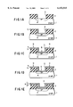
- FIGS. 1A to 1E explain how to form a barrier metal film according to an embodiment of the present invention
- FIG. 2 is a cross-sectional view of a semiconductor device formed in accordance with an embodiment of the present invention
- FIG. 3 is a schematic view of a multi-chamber type film deposition system for use in carrying out the method according to the present invention
- FIG. 4 is a view showing a structure of a Ti film forming equipment of the film deposition system shown in FIG. 3;
- FIG. 5 is a graph indicating a contact-resistance ratio versus hole size.
- FIG. 2 partly shows a cross-sectional view of the semiconductor device formed in accordance with the method of forming a multilayered film of the present invention.
- a contact hole (or via hole) 3 is formed in an insulating layer 2 so as to expose a circuit element (e.g., a diffusion layer 4 serving as an element electrode) formed in a silicon semiconductor substrate 1. Then, a contact metal (barrier metal) layer 8 constituted of a Ti film 5 and a TiN film 7 is formed on the wall of the contact hole (or via hole) 3 and the diffusion layer 4. Thereafter, an Al layer 9 serving as wiring is buried in the contact hole 3.
- a circuit element e.g., a diffusion layer 4 serving as an element electrode
- the present inventors investigated the reasons why the film removal takes place when the Ti film is nitrided by the conventional method, in order to overcome an increase of the contact resistance.
- the remaining active Ti may be oxidized and therefore the reaction with the halogen containing gas is prevented.
- the active Ti remaining on the film surface can be terminated with oxygen without fail since oxygen has a high affinity with titanium (Ti).
- TiO 2 titanium oxide
- TiO 2 titanium oxide
- Ti remaining on the TiN film surface dares to be oxidized. Since Ti not terminated with N in the nitriding process presents in few amount, little adverse effect is produced by the Ti oxidation. It is therefore possible to effectively prevent the reaction between Ti and the halogen containing gas.
- barrier metal film formation method of the present invention will be explained with reference to the manufacturing steps shown in FIGS. 1A to 1E.
- an insulating film 2 such as a silicon oxide film, is first formed on a semiconductor substrate 1 and then a contact hole 3 is formed.
- a diffusion region 4 is formed by doping impurities from the opening of the contact hole 3.
- a Ti film 5 is formed on a wall of the contact hole 3, the diffusion region 4 and the insulating layer 2.
- the Ti film 5 is formed by the PVD method or the CVD method.
- the surface of the Ti film 5 is nitrided by a nitrogen-containing processing gas to form a thin nitride film 6.
- a nitrogen-containing processing gas N 2 gas, NH 3 gas, or the like may be used. However, if a by-product is present, it will be nitrided to cause the film removal. In view of this, a N 2 -H 2 gas mixture is particularly preferable. Nitriding may be effected by only heating the substrate while supplying the nitrogen containing process gas. However, it is preferred to nitride the film in a plasma atmosphere.
- Ti active titanium
- the present invention devised that Ti not terminated with a nitrogen molecule (N) and remains on the surface of the Ti film 5, is terminated with oxygen (O) having a high affinity with Ti, by supplying an oxygen-containing gas to the Ti film 5 after the nitriding treatment.
- any gas may be used as long as it oxidizes Ti.
- active oxygen e.g. O 2 gas, air, and O 3
- H 2 O, N 2 O, NO 2 may be used.
- the temperature of oxidation treatment may be determined appropriately depending upon the type of gas; however, when O 2 gas or air is used, oxidation can be sufficiently performed at normal temperature.
- the oxidation treatment may be performed either in the Ti film deposition chamber by introducing the oxygen-containing gas therein while the semiconductor substrate placed therein after the Ti-film nitriding is completed or in the TiN film deposition chamber after the substrate is transferred to a TiN film deposition chamber.
- oxidation may be performed after completion of nitriding treatment by exposing the substrate to the air.
- a TiN film 7 is formed by the CVD method on the Ti film 5 with the nitrided film 6 interposed between them.
- TiCl 4 and either NH 3 or monomethylhydrazine (MMH) are used as the reaction gas and N 2 is used as the carrier gas.
- MMH monomethylhydrazine
- the nitrided film 6 becomes a part of the TiN film 7 by forming the TiN film 7 thereon.
- the contact metal layer 8 constituted of two layers, the Ti film 5 and the TiN film 7, is formed.
- the film thickness of Ti film 5 and TiN film 7 is set at, for example, about 50 nm each.
- the Al layer 9 serving as a wiring layer is formed on the contact metal layer 8 to thereby form the buried layer in the contact hole 3 and wiring at the same time. In this manner, the structure shown in FIG. 2 is obtained.
- the diffusion region 4 in the semiconductor substrate 1 and the wiring are electrically communicated with each other by burring the Al layer 9 into the contact hole 3.
- the material of the wiring layer is not limited to Al.
- An Al alloy, W, or a W alloy may be used.
- Application of the present invention is not limited to the contact hole and the present invention may be applied to the via-hole.
- FIG. 3 is a schematic view of a metal film deposition system by CVD for carrying out the method of the present invention.
- This system is called a cluster-tool type or a multi-chamber type.
- two load/unload cassette chambers 11, 12, a degas chamber 13, a Ti film deposition chamber 14, a pre-cleaning chamber 15, a TiN film deposition chamber 16, an Al film deposition chamber 17 and a cooling room 18 are arranged around the transfer room 10 positioned at the center with a gate valve interposed between them.
- Each of the chambers has a main chamber body having an evacuation function, inner equipment and peripheral equipment required for processing.
- FIG. 4 shows a specific structure of the film forming equipment mainly constituted of the deposition chamber 14.
- the Ti film deposition chamber 14 is constituted of a main chamber 21 of virtually a cylindrical shape.
- the semiconductor substrate W object
- the main chamber 21 constructed airtight, the semiconductor substrate W (object) is mounted horizontally on a susceptor 22 supported by cylindrical supporting members 23.
- a guide ring 24 is provided on the outer periphery of the susceptor 22, for guiding the semiconductor substrate W.
- a heater 25 is built in the susceptor 22. The heater 25 is responsible for heating the semiconductor substrate W to a predetermined temperature by supplying a current from a power source 26. The temperature of the heater 25 is controlled by a controller 27 (connected to the power supply 26) on the basis of a detection signal from a temperature sensor (not shown) attached to the main chamber.
- a shower head 30 is formed on the ceiling wall 21a of the main chamber 21 so as to face the semiconductor substrate W mounted on the susceptor 22. Numerous gas ejection holes 30a are formed in the surface of the shower head facing the substrate W. A dispersion plate 32 having numerous holes is positioned horizontally in a space 31 within the shower head 30.
- a gas inlet 33 is formed at the center of the ceiling wall 21a of the main chamber 21, for introducing a gas into the shower head 30.
- the gas supply pipe 35 is connected to the gas inlet 33.
- the gas supply pipe 35 is branched into pipes 35a to 35e which are connected to a H 2 source 36, an Ar source 37, a TiCl 4 source 38, a N 2 source 39, and an O 2 source 40, respectively.
- a desired gas is supplied from these gas sources by way of the gas supply pipe 35 and the shower head 30 into the main chamber 21.
- the nitriding is performed by supplying N 2 gas and H 2 gas respectively from the N 2 source 39 and the H 2 gas source 36. Thereafter, oxidation is performed by supplying O 2 gas from the O 2 gas source 40.
- the pipes 35a to 35e connected to the gas sources are equipped with respective valves 41a to 41e for controlling initiation/termination of gas supply, and mass-flow controllers 42a to 42e for controlling respective gas flow-rates.
- High frequency power source 44 is connected to the ceiling wall 21a of the main chamber 21 via a matching circuit 43.
- a high frequency power is introduced through the ceiling wall 21a into the main chamber 21 to form a plasma.
- the ceiling wall 21a is electrically insulated from the side wall of the main chamber 21 with an insulating member 34.
- the main chamber 21 is grounded.
- An exhaust port 28 is formed in the bottom 21b of the main chamber 21.
- the main chamber 21 is evacuated by an exhausting system 29 through the exhaust port 28 to set the inner pressure at a desired pressure.
- the TiN film deposition chamber 16 has the similar structure to the Ti film deposition chamber 14 except that a TiCl 4 source, an NH 3 source and an MMH source are provided as the gas sources.
- the Al film deposition chamber 17 has also the similar structure to the Ti film deposition chamber 14 except that gaseous dimethyl aluminum hydride (DMAH) or the like is used as a raw material and H 2 as a carrier gas.
- DMAH dimethyl aluminum hydride
- a single semiconductor substrate W is taken out from the load cassette chamber 11 by a transfer arm 19 and loaded into a pre-cleaning chamber 15 to remove a surface oxide or the like, with BrCl 3 . Subsequently, the semiconductor substrate W is transferred into the degas chamber 13 by the transfer arm 19 to degas of the semiconductor substrate W.
- the semiconductor substrate W is loaded into the main body 21 of the Ti film deposition chamber 14 by the transfer arm 19 and mounted on the susceptor 22.
- the main chamber 21 is maintained in high vacuum conditions by being evacuated by the exhaust system 9.
- the main chamber 21 is then set at a pressure of 1 Torr by introducing a process gas mixture.
- the process gas mixture containing Ar gas, H 2 gas, and TiCl 4 gas is supplied from the shower head 30 at a predetermined flow rate (e.g., Ar:1 SLM, H 2 : 1 SLM, TiCl 4 : 10 sccm), while the semiconductor substrate is maintained at a temperature from 450 to 600° C.
- a high frequency power is supplied from the high frequency power source 44 into the main chamber 21 to generate a plasma.
- the formation of the Ti film 5 on the semiconductor substrate W is performed for a predetermined time.
- the semiconductor substrate W is nitrided in the main chamber 21 while leaving it in the Ti film deposition chamber.
- the nitriding of the Ti film is performed as follows. First, a N 2 -H 2 gas mixture is supplied from the shower head 30. The N 2 gas and the H 2 gas are supplied in predetermined flow amounts, for example, 500 sccm and 1500 sccm, respectively, to set the inner pressure of the main chamber 21 at about 1 Torr. Simultaneously supplying a high frequency power from the high frequency power source into the main chamber 21 to generate a plasma. As a result of the nitriding process, a thin nitrided film 6 is formed on the surface of the Ti film 5.
- the Ti film surface is oxidized (post-nitriding oxidation) in the main chamber 21. More specifically, after the supply of N 2 gas and H 2 gas is terminated, O 2 gas is supplied into the main chamber 21 to oxidize active Ti which is not terminated with N and remains on the surface of the nitrided film 6. In this manner, active Ti is terminated with oxygen.
- the semiconductor substrate W is unloaded from the Ti deposition chamber 14 (the main chamber 21) the transfer arm 19 and transferred to the transfer chamber 10, and then, loaded into the main chamber of the TiN film deposition chamber 16.
- the TiN film deposition chamber 16 is constructed in a similar manner as the Ti film deposition chamber 14.
- the main chamber is maintained in high vacuum conditions by being evacuated by the exhausting system.
- the semiconductor substrate W is heated at, for example, 550 to 650° C. by the heater built in the susceptor.
- As the process gas either one of N 2 gas, NH 3 gas and MMH gas, or TiCl 4 gas is used.
- Each of the gases is supplied at a predetermined flow rate (for example, N 2 : 100 sccm, NH 3 : 500 sccm, TiCl 4 : 20 sccm) from the shower head to set the inner pressure of the main chamber at about 0.3 to 0.5 Torr.
- the film deposition process of the TiN film 7 is performed for a predetermined time without supplying high frequency power. As a result, the thin nitride film 6 formed on the Ti film 5 is integrated into part of the TiN film 7.
- the semiconductor substrate W is unloaded from the TiN film deposition chamber 16 and transferred into the transfer chamber 10, and then loaded into the Al film deposition chamber 17.
- the Al layer 9 is formed on the contact metal layer 8 by the CVD method using a process gas containing DMAH and H 2 gas, to thereby fill the contact hole 3 and form wiring.
- the semiconductor W having a desired structure, thus formed, is cooled in the cooling chamber 18 and stored in the unload cassette chamber 12.
- a film is formed by the CVD method in the Ti film deposition chamber 14.
- a PVD method may be used.
- oxidation is performed by supplying O 2 gas as the oxygen containing gas into the Ti film deposition chamber 14.
- oxidation may be carried out in the TiN film deposition chamber 16 by loading the semiconductor substrate W thereinto after the nitriding process before the TiN film deposition process.
- oxidation may be performed in another discrete process chamber.
- the oxidation may be performed by exposing the semiconductor substrate to the air without particularly supplying the O 2 gas.
- the semiconductor substrate W is temporarily transferred to the unload cassette chamber 12 and exposed to the air. In this case, most of the surface of the Ti film has been nitrided. Thus TiO 2 formation is limited to so small portion that it has little adverse affect on the electric contact.
- the present invention it is possible to terminate (oxidize) active Ti (not terminated in the Ti film nitriding process) in the oxidation process.
- etching of the Ti film 5 with TiCl 4 to be performed in a later TiN film forming step can be prevented.
- the thin nitride film 6 is present on the surface of the Ti film and an oxide is partly formed on the surface thereof. Since they are rarely etched with TiCl 4 , the Ti film is prevented from being etched. Accordingly, the increase of the contact resistance caused by the removal of the contact metal film can be successfully prevented.
- the Ti film of 20 nm thick is formed on the semiconductor substrate having numerous contact holes therein.
- the semiconductor substrate is nitrided in a plasma and oxidized in the air, followed by forming the TiN film of 50 nm thick thereon.
- the semiconductor substrate is nitrided in a plasma and then the TiN film is formed thereon. Both of them are measured for contact resistance.
- the results of the contact resistance measurement are shown in FIG. 5.
- the contact resistance of the semiconductor substrate receiving only nitriding treatment is represented by symbol a.
- the contact resistance of the semiconductor substrate receiving both nitriding and oxidation is represented by symbol b.
- the ratio of contact resistance (a/b) is determined with respect to each size of the holes.
- the film of the present invention formed through nitriding and oxidizing processes always exhibits a lower contact resistance.
- the advantage of the present invention is particularly apparent in the case of a hole of 0.3 ⁇ m or less, for example, the ratio of the contact resistance (a/b) exhibits 3.5 in the case of 0.25 ⁇ m-hole.
- a contact metal layer is formed in the contact hole.
- the present invention may be applied to the case where the contact metal layer is formed in a via hole.
- the case is shown where the contact metal layer is formed by stacking the TiN film on the Ti film.
- the present invention is not limited to this and may be effectively applied to the case where another film is formed on the Ti film layer by a CVD method using a halogen containing gas when the Ti film is used as an electrode or the like.
- the semiconductor substrate is used as the substrate herein.
- the present invention may be applied to an insulative substrate having a circuit element formation region made of silicon thereon, like an LCD (liquid crystal display) substrate.
- the present invention is characterized in that the semiconductor substrate is nitrided after the Ti film is formed, to terminate active Ti present in the Ti film surface with nitrogen N, and then subjected to oxidation to terminate Ti, which has not been terminated with N, with oxygen (O). It is therefore possible to prevent the Ti film from being etched in the later CVD film deposition process using halogen containing gas. As a result, it is possible to prevent an increase of contact resistance caused by the removal of the contact metal film.
Landscapes
- Engineering & Computer Science (AREA)
- Physics & Mathematics (AREA)
- Condensed Matter Physics & Semiconductors (AREA)
- General Physics & Mathematics (AREA)
- Computer Hardware Design (AREA)
- Microelectronics & Electronic Packaging (AREA)
- Power Engineering (AREA)
- Manufacturing & Machinery (AREA)
- Plasma & Fusion (AREA)
- Chemical & Material Sciences (AREA)
- Chemical Kinetics & Catalysis (AREA)
- General Chemical & Material Sciences (AREA)
- Composite Materials (AREA)
- Crystallography & Structural Chemistry (AREA)
- Internal Circuitry In Semiconductor Integrated Circuit Devices (AREA)
- Electrodes Of Semiconductors (AREA)
- Chemical Vapour Deposition (AREA)
- Other Surface Treatments For Metallic Materials (AREA)
Applications Claiming Priority (2)
| Application Number | Priority Date | Filing Date | Title |
|---|---|---|---|
| JP9-273307 | 1997-09-22 | ||
| JP27330797A JP3381767B2 (ja) | 1997-09-22 | 1997-09-22 | 成膜方法および半導体装置の製造方法 |
Publications (1)
| Publication Number | Publication Date |
|---|---|
| US6153515A true US6153515A (en) | 2000-11-28 |
Family
ID=17526053
Family Applications (1)
| Application Number | Title | Priority Date | Filing Date |
|---|---|---|---|
| US09/156,896 Expired - Fee Related US6153515A (en) | 1997-09-22 | 1998-09-18 | Method of forming multilayered film |
Country Status (4)
| Country | Link |
|---|---|
| US (1) | US6153515A (ja) |
| JP (1) | JP3381767B2 (ja) |
| KR (1) | KR100390669B1 (ja) |
| TW (1) | TW419529B (ja) |
Cited By (6)
| Publication number | Priority date | Publication date | Assignee | Title |
|---|---|---|---|---|
| KR20020053939A (ko) * | 2000-12-26 | 2002-07-06 | 박종섭 | 반도체 소자의 베리어막 형성방법 |
| US6429493B1 (en) * | 1998-10-20 | 2002-08-06 | Seiko Epson Corporation | Semiconductor device and method for manufacturing semiconductor device |
| US20040092096A1 (en) * | 2002-10-29 | 2004-05-13 | Ivo Raaijmakers | Oxygen bridge structures and methods to form oxygen bridge structures |
| US20040152300A1 (en) * | 2002-12-11 | 2004-08-05 | Kew Chan Shim | Method for forming metal wiring in a semiconductor device |
| US20050098109A1 (en) * | 1999-11-17 | 2005-05-12 | Tokyo Electron Limited | Precoat film forming method, idling method of film forming device, loading table structure, film forming device and film forming method |
| US11871563B2 (en) | 2021-06-29 | 2024-01-09 | Samsung Electronics Co., Ltd. | Method of forming contact included in semiconductor device |
Families Citing this family (5)
| Publication number | Priority date | Publication date | Assignee | Title |
|---|---|---|---|---|
| US6432479B2 (en) * | 1997-12-02 | 2002-08-13 | Applied Materials, Inc. | Method for in-situ, post deposition surface passivation of a chemical vapor deposited film |
| US7515264B2 (en) | 1999-06-15 | 2009-04-07 | Tokyo Electron Limited | Particle-measuring system and particle-measuring method |
| KR100421036B1 (ko) * | 2001-03-13 | 2004-03-03 | 삼성전자주식회사 | 웨이퍼 처리 장치 및 이를 이용한 웨이퍼 처리 방법 |
| KR100700986B1 (ko) * | 2005-08-11 | 2007-03-29 | 삼성전자주식회사 | 광학디바이스의 제조장치 및 제조방법 |
| EP2103710A4 (en) * | 2006-12-20 | 2012-11-21 | Ulvac Inc | METHOD FOR FORMING MULTILAYER FILM AND APPARATUS FOR FORMING MULTILAYER FILM |
Citations (15)
| Publication number | Priority date | Publication date | Assignee | Title |
|---|---|---|---|---|
| US5141897A (en) * | 1990-03-23 | 1992-08-25 | At&T Bell Laboratories | Method of making integrated circuit interconnection |
| US5187120A (en) * | 1992-08-24 | 1993-02-16 | Hewlett-Packard Company | Selective deposition of metal on metal nitride to form interconnect |
| US5200639A (en) * | 1990-05-31 | 1993-04-06 | Canon Kabushiki Kaisha | Semiconductor device with isolating groove containing single crystalline aluminum wiring |
| US5209816A (en) * | 1992-06-04 | 1993-05-11 | Micron Technology, Inc. | Method of chemical mechanical polishing aluminum containing metal layers and slurry for chemical mechanical polishing |
| US5217756A (en) * | 1990-06-08 | 1993-06-08 | Nec Corporation | Selective chemical vapor deposition of aluminum, aluminum CVD materials and process for preparing the same |
| US5231056A (en) * | 1992-01-15 | 1993-07-27 | Micron Technology, Inc. | Tungsten silicide (WSix) deposition process for semiconductor manufacture |
| US5270254A (en) * | 1991-03-27 | 1993-12-14 | Sgs-Thomson Microelectronics, Inc. | Integrated circuit metallization with zero contact enclosure requirements and method of making the same |
| US5288665A (en) * | 1992-08-12 | 1994-02-22 | Applied Materials, Inc. | Process for forming low resistance aluminum plug in via electrically connected to overlying patterned metal layer for integrated circuit structures |
| US5330921A (en) * | 1991-03-19 | 1994-07-19 | Matsushita Electric Industrial Co., Ltd. | Method of fabricating semiconductor device |
| US5344792A (en) * | 1993-03-04 | 1994-09-06 | Micron Technology, Inc. | Pulsed plasma enhanced CVD of metal silicide conductive films such as TiSi2 |
| US5663097A (en) * | 1991-06-21 | 1997-09-02 | Canon Kabushiki Kaisha | Method of fabricating a semiconductor device having an insulating side wall |
| US5834846A (en) * | 1995-01-10 | 1998-11-10 | Kawasaki Steel Corporation | Semiconductor device with contact structure and method of manufacturing the same |
| US5858184A (en) * | 1995-06-07 | 1999-01-12 | Applied Materials, Inc. | Process for forming improved titanium-containing barrier layers |
| US5869901A (en) * | 1995-10-17 | 1999-02-09 | Nissan Motor Co., Ltd. | Semiconductor device having aluminum interconnection and method of manufacturing the same |
| US5877086A (en) * | 1996-07-12 | 1999-03-02 | Applied Materials, Inc. | Metal planarization using a CVD wetting film |
-
1997
- 1997-09-22 JP JP27330797A patent/JP3381767B2/ja not_active Expired - Fee Related
-
1998
- 1998-09-18 US US09/156,896 patent/US6153515A/en not_active Expired - Fee Related
- 1998-09-18 TW TW087115611A patent/TW419529B/zh not_active IP Right Cessation
- 1998-09-22 KR KR10-1998-0039185A patent/KR100390669B1/ko not_active IP Right Cessation
Patent Citations (15)
| Publication number | Priority date | Publication date | Assignee | Title |
|---|---|---|---|---|
| US5141897A (en) * | 1990-03-23 | 1992-08-25 | At&T Bell Laboratories | Method of making integrated circuit interconnection |
| US5200639A (en) * | 1990-05-31 | 1993-04-06 | Canon Kabushiki Kaisha | Semiconductor device with isolating groove containing single crystalline aluminum wiring |
| US5217756A (en) * | 1990-06-08 | 1993-06-08 | Nec Corporation | Selective chemical vapor deposition of aluminum, aluminum CVD materials and process for preparing the same |
| US5330921A (en) * | 1991-03-19 | 1994-07-19 | Matsushita Electric Industrial Co., Ltd. | Method of fabricating semiconductor device |
| US5270254A (en) * | 1991-03-27 | 1993-12-14 | Sgs-Thomson Microelectronics, Inc. | Integrated circuit metallization with zero contact enclosure requirements and method of making the same |
| US5663097A (en) * | 1991-06-21 | 1997-09-02 | Canon Kabushiki Kaisha | Method of fabricating a semiconductor device having an insulating side wall |
| US5231056A (en) * | 1992-01-15 | 1993-07-27 | Micron Technology, Inc. | Tungsten silicide (WSix) deposition process for semiconductor manufacture |
| US5209816A (en) * | 1992-06-04 | 1993-05-11 | Micron Technology, Inc. | Method of chemical mechanical polishing aluminum containing metal layers and slurry for chemical mechanical polishing |
| US5288665A (en) * | 1992-08-12 | 1994-02-22 | Applied Materials, Inc. | Process for forming low resistance aluminum plug in via electrically connected to overlying patterned metal layer for integrated circuit structures |
| US5187120A (en) * | 1992-08-24 | 1993-02-16 | Hewlett-Packard Company | Selective deposition of metal on metal nitride to form interconnect |
| US5344792A (en) * | 1993-03-04 | 1994-09-06 | Micron Technology, Inc. | Pulsed plasma enhanced CVD of metal silicide conductive films such as TiSi2 |
| US5834846A (en) * | 1995-01-10 | 1998-11-10 | Kawasaki Steel Corporation | Semiconductor device with contact structure and method of manufacturing the same |
| US5858184A (en) * | 1995-06-07 | 1999-01-12 | Applied Materials, Inc. | Process for forming improved titanium-containing barrier layers |
| US5869901A (en) * | 1995-10-17 | 1999-02-09 | Nissan Motor Co., Ltd. | Semiconductor device having aluminum interconnection and method of manufacturing the same |
| US5877086A (en) * | 1996-07-12 | 1999-03-02 | Applied Materials, Inc. | Metal planarization using a CVD wetting film |
Cited By (13)
| Publication number | Priority date | Publication date | Assignee | Title |
|---|---|---|---|---|
| US6429493B1 (en) * | 1998-10-20 | 2002-08-06 | Seiko Epson Corporation | Semiconductor device and method for manufacturing semiconductor device |
| US6511910B2 (en) | 1998-10-20 | 2003-01-28 | Seiko Epson Corporation | Method for manufacturing semiconductor devices |
| US20050098109A1 (en) * | 1999-11-17 | 2005-05-12 | Tokyo Electron Limited | Precoat film forming method, idling method of film forming device, loading table structure, film forming device and film forming method |
| US20080226822A1 (en) * | 1999-11-17 | 2008-09-18 | Satoshi Wakabayashi | Precoat film forming method, idling method of film forming device, loading table structure, film forming device and film forming method |
| KR20020053939A (ko) * | 2000-12-26 | 2002-07-06 | 박종섭 | 반도체 소자의 베리어막 형성방법 |
| US20060258150A1 (en) * | 2002-10-29 | 2006-11-16 | Ivo Raaijmakers | Oxygen bridge structures and methods to form oxygen bridge structures |
| US7034397B2 (en) | 2002-10-29 | 2006-04-25 | Asm Internationl, N.V. | Oxygen bridge structures and methods to form oxygen bridge structures |
| WO2004040642A1 (en) * | 2002-10-29 | 2004-05-13 | Asm America, Inc. | Oxygen bridge structures and methods |
| US20040092096A1 (en) * | 2002-10-29 | 2004-05-13 | Ivo Raaijmakers | Oxygen bridge structures and methods to form oxygen bridge structures |
| US7465658B2 (en) | 2002-10-29 | 2008-12-16 | Asm America, Inc. | Oxygen bridge structures and methods to form oxygen bridge structures |
| US6812144B2 (en) * | 2002-12-11 | 2004-11-02 | Hynix Semiconductor Inc. | Method for forming metal wiring in a semiconductor device |
| US20040152300A1 (en) * | 2002-12-11 | 2004-08-05 | Kew Chan Shim | Method for forming metal wiring in a semiconductor device |
| US11871563B2 (en) | 2021-06-29 | 2024-01-09 | Samsung Electronics Co., Ltd. | Method of forming contact included in semiconductor device |
Also Published As
| Publication number | Publication date |
|---|---|
| JPH1197386A (ja) | 1999-04-09 |
| KR100390669B1 (ko) | 2003-08-19 |
| TW419529B (en) | 2001-01-21 |
| KR19990030018A (ko) | 1999-04-26 |
| JP3381767B2 (ja) | 2003-03-04 |
Similar Documents
| Publication | Publication Date | Title |
|---|---|---|
| US8440563B2 (en) | Film forming method and processing system | |
| US6326690B2 (en) | Method of titanium/titanium nitride integration | |
| US8207061B2 (en) | Semiconductor device manufacturing method using valve metal and nitride of valve metal | |
| US6218301B1 (en) | Deposition of tungsten films from W(CO)6 | |
| US6051281A (en) | Method of forming a titanium film and a barrier metal film on a surface of a substrate through lamination | |
| EP1063686A2 (en) | Method of silicide formation in a semiconductor device | |
| KR101210456B1 (ko) | 반도체 장치의 제조 방법, 기판 처리 방법 및 기판 처리 장치 | |
| JPH11195621A (ja) | バリアメタル、その形成方法、ゲート電極及びその形成方法 | |
| US20090071404A1 (en) | Method of forming titanium film by CVD | |
| US11152260B2 (en) | Embedding method and processing system | |
| US20200083098A1 (en) | Embedding Method and Processing System | |
| US6153515A (en) | Method of forming multilayered film | |
| US20080184543A1 (en) | Method and apparatus for manufacturing semiconductor device, and storage medium for executing the method | |
| US20050089634A1 (en) | Method for depositing metallic nitride series thin film | |
| WO2008010371A1 (fr) | Procédé de fabrication de dispositif semi-conducteur, appareil de fabrication de dispositif semi-conducteur, programme informatique et support de stockage | |
| US6197674B1 (en) | CVD-Ti film forming method | |
| JP3578155B2 (ja) | 被処理体の酸化方法 | |
| JP4151308B2 (ja) | 処理装置のガス導入方法 | |
| US6537621B1 (en) | Method of forming a titanium film and a barrier film on a surface of a substrate through lamination | |
| US6180513B1 (en) | Apparatus and method for manufacturing a semiconductor device having a multi-wiring layer structure | |
| JPH0661229A (ja) | 半導体装置の製造方法 | |
| KR20010007527A (ko) | 반도체 장치내에 실리사이드를 형성하는 방법 및 이를이용한 프로세서 판독가능 저장매체 | |
| JP3767429B2 (ja) | チタン膜及びチタンナイトライド膜の連続成膜方法及びクラスタツール装置 | |
| US20240105445A1 (en) | Film forming method and substrate processing system | |
| WO1999035675A1 (fr) | Procede pour former un film de titane par d.c.p.v. |
Legal Events
| Date | Code | Title | Description |
|---|---|---|---|
| AS | Assignment |
Owner name: TOKYO ELECTRON LIMITED, JAPAN Free format text: ASSIGNMENT OF ASSIGNORS INTEREST;ASSIGNORS:MURAKAMI, SEISHI;HATANO, TATSUO;REEL/FRAME:009484/0357 Effective date: 19980907 |
|
| AS | Assignment |
Owner name: TOKYO ELECTRON LIMITED, JAPAN Free format text: ASSIGNMENT OF ASSIGNOR'S INTEREST RE-RECORD TO CORRECT THE RECORDATION DATE OF 09/16/98 TO 09/18/98 PREVIOUSLY RECORDED AT REEL9484, FRAME 0357;ASSIGNORS:MURAKAMI, SEISHI;HATANO, TATSUO;REEL/FRAME:009923/0789 Effective date: 19980907 |
|
| FEPP | Fee payment procedure |
Free format text: PAYOR NUMBER ASSIGNED (ORIGINAL EVENT CODE: ASPN); ENTITY STATUS OF PATENT OWNER: LARGE ENTITY |
|
| FPAY | Fee payment |
Year of fee payment: 4 |
|
| FPAY | Fee payment |
Year of fee payment: 8 |
|
| REMI | Maintenance fee reminder mailed | ||
| LAPS | Lapse for failure to pay maintenance fees | ||
| STCH | Information on status: patent discontinuation |
Free format text: PATENT EXPIRED DUE TO NONPAYMENT OF MAINTENANCE FEES UNDER 37 CFR 1.362 |
|
| FP | Lapsed due to failure to pay maintenance fee |
Effective date: 20121128 |