US6150183A - Method for manufacturing metal oxide capacitor and method for manufacturing semiconductor memory device - Google Patents
Method for manufacturing metal oxide capacitor and method for manufacturing semiconductor memory device Download PDFInfo
- Publication number
- US6150183A US6150183A US08/993,873 US99387397A US6150183A US 6150183 A US6150183 A US 6150183A US 99387397 A US99387397 A US 99387397A US 6150183 A US6150183 A US 6150183A
- Authority
- US
- United States
- Prior art keywords
- metal oxide
- electrode
- capacitor
- oxide film
- manufacturing
- Prior art date
- Legal status (The legal status is an assumption and is not a legal conclusion. Google has not performed a legal analysis and makes no representation as to the accuracy of the status listed.)
- Expired - Lifetime
Links
- 239000003990 capacitor Substances 0.000 title claims abstract description 55
- 229910044991 metal oxide Inorganic materials 0.000 title claims abstract description 44
- 150000004706 metal oxides Chemical class 0.000 title claims abstract description 44
- 238000000034 method Methods 0.000 title claims description 49
- 238000004519 manufacturing process Methods 0.000 title claims description 30
- 239000004065 semiconductor Substances 0.000 title claims description 10
- QVGXLLKOCUKJST-UHFFFAOYSA-N atomic oxygen Chemical compound [O] QVGXLLKOCUKJST-UHFFFAOYSA-N 0.000 claims abstract description 48
- 239000001301 oxygen Substances 0.000 claims abstract description 48
- 229910052760 oxygen Inorganic materials 0.000 claims abstract description 48
- 229910052751 metal Inorganic materials 0.000 claims description 35
- 239000002184 metal Substances 0.000 claims description 35
- 230000004888 barrier function Effects 0.000 claims description 29
- 238000010438 heat treatment Methods 0.000 claims description 9
- 239000000758 substrate Substances 0.000 claims description 8
- 229910010252 TiO3 Inorganic materials 0.000 claims description 7
- 229910020279 Pb(Zr, Ti)O3 Inorganic materials 0.000 claims description 6
- 229910004446 Ta2 O5 Inorganic materials 0.000 claims description 6
- 239000000463 material Substances 0.000 claims description 6
- 150000004767 nitrides Chemical class 0.000 claims description 5
- 229910000510 noble metal Inorganic materials 0.000 claims description 5
- 238000004377 microelectronic Methods 0.000 claims 2
- 238000010030 laminating Methods 0.000 abstract 1
- 239000010408 film Substances 0.000 description 32
- 238000007254 oxidation reaction Methods 0.000 description 20
- 230000003647 oxidation Effects 0.000 description 18
- VYPSYNLAJGMNEJ-UHFFFAOYSA-N Silicium dioxide Chemical compound O=[Si]=O VYPSYNLAJGMNEJ-UHFFFAOYSA-N 0.000 description 16
- ATJFFYVFTNAWJD-UHFFFAOYSA-N Tin Chemical compound [Sn] ATJFFYVFTNAWJD-UHFFFAOYSA-N 0.000 description 14
- 238000005229 chemical vapour deposition Methods 0.000 description 11
- 229910052681 coesite Inorganic materials 0.000 description 8
- 229910052906 cristobalite Inorganic materials 0.000 description 8
- 239000000377 silicon dioxide Substances 0.000 description 8
- 229910052682 stishovite Inorganic materials 0.000 description 8
- 229910052905 tridymite Inorganic materials 0.000 description 8
- 230000015572 biosynthetic process Effects 0.000 description 6
- 238000004544 sputter deposition Methods 0.000 description 6
- 238000009792 diffusion process Methods 0.000 description 5
- 229910052741 iridium Inorganic materials 0.000 description 5
- 229910021420 polycrystalline silicon Inorganic materials 0.000 description 5
- 229920005591 polysilicon Polymers 0.000 description 5
- 239000010409 thin film Substances 0.000 description 5
- GWEVSGVZZGPLCZ-UHFFFAOYSA-N Titan oxide Chemical compound O=[Ti]=O GWEVSGVZZGPLCZ-UHFFFAOYSA-N 0.000 description 4
- 230000000694 effects Effects 0.000 description 4
- 229910052697 platinum Inorganic materials 0.000 description 4
- 229910052707 ruthenium Inorganic materials 0.000 description 4
- 238000003980 solgel method Methods 0.000 description 4
- 238000000137 annealing Methods 0.000 description 3
- 238000010586 diagram Methods 0.000 description 3
- 238000000059 patterning Methods 0.000 description 3
- 229920002120 photoresistant polymer Polymers 0.000 description 3
- 238000001020 plasma etching Methods 0.000 description 3
- 229910052710 silicon Inorganic materials 0.000 description 3
- 239000010703 silicon Substances 0.000 description 3
- 238000002441 X-ray diffraction Methods 0.000 description 2
- 238000006243 chemical reaction Methods 0.000 description 2
- 239000003989 dielectric material Substances 0.000 description 2
- 239000007772 electrode material Substances 0.000 description 2
- 239000007789 gas Substances 0.000 description 2
- 239000012535 impurity Substances 0.000 description 2
- 238000009413 insulation Methods 0.000 description 2
- 238000005498 polishing Methods 0.000 description 2
- 125000006850 spacer group Chemical group 0.000 description 2
- 238000003860 storage Methods 0.000 description 2
- 239000000126 substance Substances 0.000 description 2
- 108010053481 Antifreeze Proteins Proteins 0.000 description 1
- 229910007277 Si3 N4 Inorganic materials 0.000 description 1
- XUIMIQQOPSSXEZ-UHFFFAOYSA-N Silicon Chemical compound [Si] XUIMIQQOPSSXEZ-UHFFFAOYSA-N 0.000 description 1
- 229910004166 TaN Inorganic materials 0.000 description 1
- 229910004200 TaSiN Inorganic materials 0.000 description 1
- 229910010037 TiAlN Inorganic materials 0.000 description 1
- -1 TiN and TaN is used Chemical class 0.000 description 1
- 239000011248 coating agent Substances 0.000 description 1
- 238000000576 coating method Methods 0.000 description 1
- 230000008094 contradictory effect Effects 0.000 description 1
- 238000001312 dry etching Methods 0.000 description 1
- 239000012789 electroconductive film Substances 0.000 description 1
- 238000005530 etching Methods 0.000 description 1
- 230000002349 favourable effect Effects 0.000 description 1
- 230000006870 function Effects 0.000 description 1
- 239000011261 inert gas Substances 0.000 description 1
- 238000003475 lamination Methods 0.000 description 1
- 239000000203 mixture Substances 0.000 description 1
- 125000004430 oxygen atom Chemical group O* 0.000 description 1
- 229910052814 silicon oxide Inorganic materials 0.000 description 1
- 238000001228 spectrum Methods 0.000 description 1
- 230000001629 suppression Effects 0.000 description 1
- OGIDPMRJRNCKJF-UHFFFAOYSA-N titanium oxide Inorganic materials [Ti]=O OGIDPMRJRNCKJF-UHFFFAOYSA-N 0.000 description 1
- 229910052726 zirconium Inorganic materials 0.000 description 1
Images


Classifications
-
- H—ELECTRICITY
- H01—ELECTRIC ELEMENTS
- H01L—SEMICONDUCTOR DEVICES NOT COVERED BY CLASS H10
- H01L21/00—Processes or apparatus adapted for the manufacture or treatment of semiconductor or solid state devices or of parts thereof
- H01L21/02—Manufacture or treatment of semiconductor devices or of parts thereof
- H01L21/02104—Forming layers
- H01L21/02107—Forming insulating materials on a substrate
- H01L21/02109—Forming insulating materials on a substrate characterised by the type of layer, e.g. type of material, porous/non-porous, pre-cursors, mixtures or laminates
- H01L21/02112—Forming insulating materials on a substrate characterised by the type of layer, e.g. type of material, porous/non-porous, pre-cursors, mixtures or laminates characterised by the material of the layer
- H01L21/02172—Forming insulating materials on a substrate characterised by the type of layer, e.g. type of material, porous/non-porous, pre-cursors, mixtures or laminates characterised by the material of the layer the material containing at least one metal element, e.g. metal oxides, metal nitrides, metal oxynitrides or metal carbides
- H01L21/02197—Forming insulating materials on a substrate characterised by the type of layer, e.g. type of material, porous/non-porous, pre-cursors, mixtures or laminates characterised by the material of the layer the material containing at least one metal element, e.g. metal oxides, metal nitrides, metal oxynitrides or metal carbides the material having a perovskite structure, e.g. BaTiO3
-
- H—ELECTRICITY
- H01—ELECTRIC ELEMENTS
- H01L—SEMICONDUCTOR DEVICES NOT COVERED BY CLASS H10
- H01L21/00—Processes or apparatus adapted for the manufacture or treatment of semiconductor or solid state devices or of parts thereof
- H01L21/02—Manufacture or treatment of semiconductor devices or of parts thereof
- H01L21/02104—Forming layers
- H01L21/02107—Forming insulating materials on a substrate
- H01L21/02225—Forming insulating materials on a substrate characterised by the process for the formation of the insulating layer
- H01L21/0226—Forming insulating materials on a substrate characterised by the process for the formation of the insulating layer formation by a deposition process
- H01L21/02263—Forming insulating materials on a substrate characterised by the process for the formation of the insulating layer formation by a deposition process deposition from the gas or vapour phase
- H01L21/02266—Forming insulating materials on a substrate characterised by the process for the formation of the insulating layer formation by a deposition process deposition from the gas or vapour phase deposition by physical ablation of a target, e.g. sputtering, reactive sputtering, physical vapour deposition or pulsed laser deposition
-
- H—ELECTRICITY
- H01—ELECTRIC ELEMENTS
- H01L—SEMICONDUCTOR DEVICES NOT COVERED BY CLASS H10
- H01L21/00—Processes or apparatus adapted for the manufacture or treatment of semiconductor or solid state devices or of parts thereof
- H01L21/02—Manufacture or treatment of semiconductor devices or of parts thereof
- H01L21/04—Manufacture or treatment of semiconductor devices or of parts thereof the devices having potential barriers, e.g. a PN junction, depletion layer or carrier concentration layer
- H01L21/18—Manufacture or treatment of semiconductor devices or of parts thereof the devices having potential barriers, e.g. a PN junction, depletion layer or carrier concentration layer the devices having semiconductor bodies comprising elements of Group IV of the Periodic Table or AIIIBV compounds with or without impurities, e.g. doping materials
- H01L21/30—Treatment of semiconductor bodies using processes or apparatus not provided for in groups H01L21/20 - H01L21/26
- H01L21/31—Treatment of semiconductor bodies using processes or apparatus not provided for in groups H01L21/20 - H01L21/26 to form insulating layers thereon, e.g. for masking or by using photolithographic techniques; After treatment of these layers; Selection of materials for these layers
- H01L21/314—Inorganic layers
- H01L21/316—Inorganic layers composed of oxides or glassy oxides or oxide based glass
- H01L21/31691—Inorganic layers composed of oxides or glassy oxides or oxide based glass with perovskite structure
-
- H—ELECTRICITY
- H01—ELECTRIC ELEMENTS
- H01L—SEMICONDUCTOR DEVICES NOT COVERED BY CLASS H10
- H01L28/00—Passive two-terminal components without a potential-jump or surface barrier for integrated circuits; Details thereof; Multistep manufacturing processes therefor
- H01L28/40—Capacitors
- H01L28/55—Capacitors with a dielectric comprising a perovskite structure material
Definitions
- the present invention pertains to a method for manufacturing a metal oxide capacitor (in particular, high-dielectric capacitor such as (Ba, Sr)TiO 3 or ferroelectric capacitor such as Pb(Zr, Ti)O 3 ) and a method for manufacturing a semiconductor memory device having the metal oxide capacitor.
- a metal oxide capacitor in particular, high-dielectric capacitor such as (Ba, Sr)TiO 3 or ferroelectric capacitor such as Pb(Zr, Ti)O 3
- a capacitor dielectric film for forming a cell capacity of a memory cell of a DRAM (Dynamic Random Access Memory) as a semiconductor memory As a conventional capacitor dielectric film for forming a cell capacity of a memory cell of a DRAM (Dynamic Random Access Memory) as a semiconductor memory, an ONO film in which SiO 2 , Si 3 N 4 , and SiO 2 are sequentially laminated is used.
- the effective relative dielectric constant of the ONO film is as small as about 5, and in case it is applied to a large-capacity memory of 256 Mbit or less, the process is considerably difficult.
- an insulating metal oxide represented by Ta 2 O 5 , (Ba, Sr)TiO 3 (hereinafter, abbreviated to BST), and Pb(Zr, Ti)O 3 (hereinafter, abbreviated to PZT) has a large relative dielectric constant from several tens to several hundreds, a capacitor dielectric material for a future DRAM is noticed.
- a lower electrode 38 (using a noble metal such as Pt, Ir, and Ru in terms of oxidation resistance) is laminated on a barrier metal layer 39 (using a nitride such as TiN and TaN in terms of oxidation resistance) for preventing the diffusion of an electrode-constituting component, and a BST high-dielectric thin-film 40 is formed on the lower electrode 38 by sputtering method, chemical vapor deposition method (CVD), or sol-gel method. Furthermore, an upper electrode 37 (using a noble metal such as Pt, Ir, and Ru similarly to the lower electrode 38) is formed in almost the same pattern as the above.
- a noble metal such as Pt, Ir, and Ru in terms of oxidation resistance
- a spacer (side wall for securing insulation) 35 composed of a silicon oxide film is formed. Also, the lower electrode 38 is connected to a silicon substrate side via a metal layer (plug) 8 such as polysilicon as a storage node embedded in a contact hole 14 of an insulating film 7 such as SiO 2 .
- a metal layer (plug) 8 such as polysilicon as a storage node embedded in a contact hole 14 of an insulating film 7 such as SiO 2 .
- a memory cell of the DRAM having the high-dielectric capacitor is explained.
- an element area divided by a field oxide film 2 is formed on one principal plane of a P - silicon substrate, and a transfer gate TR consisting of a MOS transistor and a memory cell M-Cel consisting of the high-dielectric capacitor Cap are installed in it.
- the memory cell is a CUB (Cell under Bitline) type.
- N + drain region 3 and N + source region 4 are respectively formed by an impurity diffusion, and a word line 6 (WL) is installed via a gate oxide film 5 between these two regions.
- a bit line 24 (BL) is connected via a contact hole 16 of insulating layers 7 and 47 such as SiO 2 to the drain region 3.
- a thin BST film 40 is formed by CVD method, sputtering method, sol-gel method, etc.; however, its formation is carried out in an oxygen atmosphere. Furthermore, after forming a capacitor, a heat treatment (hereinafter, called a postannealing) [is carried out] in an oxygen atmosphere of 1 atm to improve its leakage current characteristic and dielectric characteristic.
- a postannealing a heat treatment
- FIG. 17 shows a relationship between the current-voltage characteristic and the postannealing temperature (500° C., 700° C.) of a BST capacitor, in which the BST film 40 is formed at a film thickness of 25 nm on the Pt lower electrode 38 at a substrate temperature of 550° C. by a sputtering method.
- the upper electrode is Pt
- the postannealing time is 30 min.
- the leakage current characteristic after postannealing is largely improved. Also, the higher the postannealing temperature, the smaller the leakage current density.
- the leakage current characteristic of the capacitor is markedly improved by postannealing, and as the treatment temperature increases, a large effect is obtained.
- a barrier metal 39 of FIG. 16 is oxidized in the meantime, so that TiO 2 , for instance, is formed.
- the reason for this is considered that an oxygen atom diffuses up to the interface with the barrier metal 39 through a grain boundary of the lower electrode 38 and the barrier metal is oxidized. If the postannealing [temperature] is increased, such a phenomenon is accelerated. Also, it is considered that if the grain size of the lower electrode 38 is small, the oxygen is easily diffused.
- the oxygen diffusion can be suppressed by increasing the grain size to 1000 ⁇ or more, for instance, by raising the formation temperature of the lower electrode (furthermore, the leakage current is also reduced); however, if the grain size is increased, if the patterning due to a dry etching is difficult, the lower electrode is usually formed so that the grain size can be about 500 ⁇ from this viewpoint. Thus, the suppression effect of the oxygen diffusion is weakened.
- the nitride such as TiN and TaN as a barrier metal is oxidized, since it is changed to an insulating oxide, an inferior electrification between the plug 8 and the lower electrode 38 is caused. Therefore, it is necessary to set the postannealing temperature sufficiently lower than the oxidation temperature of the nitride such as TiN and TaN. This is a condition contradictory to the leakage current reduction effect shown in FIG. 17 due to the increase of the postannealing temperature.
- FIG. 18 shows a result in which the oxidation start temperature of TiN (barrier metal: a film thickness of 1000 ⁇ ) in the lamination structure composed of Pt/TiN/Si is investigated by an X-ray diffraction method. According to the figure, a diffraction peak of TiO 2 showing the oxidation start of TiN starts to be seen at near 600° C. From the result, in case TiN is used as a barrier metal, the postannealing temperature is limited to 600° C. or lower.
- the purpose of the present invention is to provide a method for manufacturing a metal oxide barrier such as BST, which can effectively suppress the oxidation of an undercoat metal such as a barrier metal while reducing the heat treatment temperature such as the postannealing temperature and a method for manufacturing a semiconductor memory device having the metal oxide capacitor.
- the present invention provides a method for manufacturing a metal oxide capacitor, which is characterized by the fact that in manufacturing a metal oxide capacitor in which a metal oxide film and a second electrode are sequentially laminated on a first electrode, the above-mentioned metal oxide film is formed and then heat treated (high-pressure oxygen postannealing) in an atmosphere with an oxygen pressure higher than 1 atm (in particular, 2-100 atm), and a method for manufacturing a semiconductor memory device, which manufactures the metal oxide capacitor.
- the high-pressure oxygen postannealing by the method for manufacturing a metal oxide capacitor and the method for manufacturing a semiconductor device (hereinafter, sometimes called the method of the present invention) is very effective for the reduction of the postannealing temperature and is very effective for avoiding the oxidation caused during the postannealing of TiN and TaN used as a conventional barrier metal.
- the effects of the method of the present invention are considered by the following oxidation reaction of TiN as an example.
- oxygen is provided by being diffused into the upper Pt electrode and BST, it is considered as an atomic state. Therefore, the oxidation reaction of TiN is expressed by the following formula.
- reaction velocity of the oxidation is proportional to the square of the partial oxygen pressure.
- reaction velocity depends exponentially on the temperature. For this reason, it is favorable to set the oxygen pressure high at lower temperature (that is, by a high-pressure oxygen annealing) rather than to set the temperature high during the postannealing, since the oxidation rate of the barrier metal is suppressed.
- the oxidation of the barrier metal can be suppressed by the high-pressure oxygen annealing rather than by setting the postannealing temperature high, the oxidation of the barrier metal can be controlled to be more difficult while setting the temperature (preferably 550° C. or less, more preferably 350-500° C.), at which the oxidation of the barrier metal is difficult to be generated, by lowering the postannealing temperature.
- the temperature preferably 550° C. or less, more preferably 350-500° C.
- the postannealing it is preferable to carry out the postannealing at an oxygen pressure of 2-100 atm. If the oxygen pressure is less than 2 atm, the postannealing of the above-mentioned metal oxide film is not sufficient, even in a pressurized state. Also, if the oxygen pressure is more than 100 atm, the annealing is sufficient due to the high pressure; however, it is more dangerous for a work environment. Furthermore, it is preferable to carry out the postannealing at an oxygen pressure of 2-10 atm.
- the applicable oxygen atmosphere in the method of the present invention may be an atmosphere of oxygen alone or a mixture of oxygen and an inert gas such as N 2 and Ar.
- the oxygen pressure is a gas pressure of the oxygen atmosphere itself for the oxygen alone and is a partial oxygen pressure for a mixed gas.
- the above-mentioned first electrode is formed on the barrier metal, and the above-mentioned metal oxide film is formed in an oxygen atmosphere on the first electrode. Then, the above-mentioned second electrode is formed on the metal oxide film, and the above-mentioned heat treatment can be carried out. Or, the above-mentioned first electrode is formed on the barrier metal, and the above-mentioned metal oxide film is formed in an oxygen atmosphere on the first electrode. Then, the above-mentioned heat treatment can be carried out.
- a metal oxide such as TiN and TaN
- a noble metal such as Pt, Ir, and Ru
- the above-mentioned metal oxide film (Ba, Sr)TiO 3 , Pb(Zr, Ti)O 3 , or Ta 2 O 5 can be used.
- the metal oxide film can be formed by the well-known CVD method, sputtering, or sol-gel method.
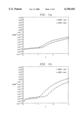
- FIGS. 1a-1b is a characteristic diagram showing a comparison of the current-voltage characteristic after applying a postannealing in an atmosphere of different oxygen pressures to a capacitor with a Pt/BST/Pt structure in the embodiment of the present invention.
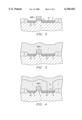
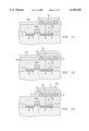
- FIG. 2 is an outlined cross section at one stage in a process for manufacturing a memory cell having the same capacitor.
- FIG. 3 is an outlined cross section at another stage in a process for manufacturing a memory cell having the same capacitor.
- FIG. 4 is an outlined cross section at another stage in a process for manufacturing a memory cell having the same capacitor.
- FIG. 5 is an outlined cross section at another stage in a process for manufacturing a memory cell having the same capacitor.
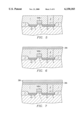
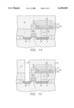
- FIG. 6 is an outlined cross section at another stage in a process for manufacturing a memory cell having the same capacitor.
- FIG. 7 is an outlined cross section at another stage in a process for manufacturing a memory cell having the same capacitor.
- FIG. 8 is an outlined cross section at another stage in a process for manufacturing a memory cell having the same capacitor.
- FIG. 9 is an outlined cross section at another stage in a process for manufacturing a memory cell having the same capacitor.
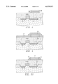
- FIG. 10 is an outlined cross section at another stage in a process for manufacturing a memory cell having the same capacitor.
- FIG. 11 is an outlined cross section at another stage in a process for manufacturing a memory cell having the same capacitor.
- FIG. 12 is an outlined cross section at another stage in a process for manufacturing a memory cell having the same capacitor.
- FIG. 13 is an outlined cross section at another stage in a process for manufacturing a memory cell having the same capacitor.
- FIG. 14 is an outlined cross section at another stage in a process for manufacturing a memory cell having the same capacitor.
- FIG. 15 is an outlined cross section at another stage in a process for manufacturing a memory cell having the same capacitor.
- FIG. 16 is an outlined cross section of a conventional memory cell having a capacitor with a Pt/BST/Pt structure.
- FIG. 17 is a characteristic diagram showing a comparison of the current-voltage characteristic after applying a postannealing at different temperatures to the same capacitor.
- FIG. 18 is an X-ray diffraction spectrum diagram showing a temperature dependency of the oxidation of TiN on a Pt/TiN/Si structure.
- 3 represents source region, 4 a drain region, 6 a word line, 7, 47 an insulating layers, 8 a polysilicon plug, 24 a bit line, 35 a side wall, 37 an upper electrode, 38 a lower electrode, 39 a barrier metal, 40 a high-dielectric film, Cap, CAP a metal oxide thin-film (high-dielectric) capacitor, M-Cel a memory cell.
- a field oxide film 2 is formed on a P - silicon substrate (wafer) 1 by a selective oxidation method; and a gate oxide film 5 by a thermal oxide method and a polysilicon word line 6 (WL) by a chemical vapor deposition method are respectively formed.
- a N + drain region 3 and a source region 4 are respectively formed by thermal diffusion of an N-type impurity such as As.
- a SiO 2 insulating layer 7 is deposited on the entire surface by the chemical vapor deposition method, and the insulating layer 7 is etched using a photoresist mask (not shown in the figure). As shown in FIG. 4, a contact hole 14 is formed in a prescribed shape on the source region 4.
- a polysilicon layer 8 is deposited by chemical vapor deposition so that it contacts the source region 4 in the contact hole 14.
- the polysilicon layer 8 as a storage node and the SiO 2 layer 7 are etched by a chemical mechanical polishing (CMP: Chemical Mechanical Polishing/Planarization) or an etch back due to plasma etching, so that the surface is flattened.
- CMP Chemical Mechanical Polishing/Planarization
- planarization is not carried out, that is, if the upper layer is laminated with a level difference, the coating characteristic of the upper layer will be deteriorated, so that leakage current and peeling-off of the film are generated.
- a material 39A for a barrier metal layer composed of a TiN layer is sputtered or vapor-deposited as shown in FIG. 6 on the flattened surface, and a lower electrode material layer 38A composed of Pt is sputtered or vapor-deposited as shown in FIG. 7.
- the thickness of the material 39A for a barrier metal layer is set to 200-2000 ⁇ , which is sufficient for generating the function of a barrier metal.
- the lower electrode 38 and the barrier metal layer 39 are etched in almost the same pattern.
- a Sio 2 [layer] 35A for forming a spacer (side wall for securing the insulation) is formed by chemical vapor deposition, and a SiO 2 spacer 35 with a prescribed shape is formed as a side wall as shown in FIG. 10 by the etch back due to an anisotropic plasma etching.
- a high-dielectric material 40A composed of a BST (Ba, Sr) TiO 3 film is formed by a sputtering method or CVD method, and as shown in FIG. 12, an upper electrode material layer 37A composed of Pt or Ir is sputtered or vapor-deposited on it.
- the upper electrode 37 and the high-dielectric film 40 are formed in a prescribed pattern by patterning through etching using the photoresist mask (not shown in the figure), so that a BST high-dielectric thin-film capacitor CAP is manufactured.
- a high-pressure oxygen postannealing is applied at 550° C. or lower (for example, 500° C.) for 10-240 min (for example, 30 min) to the capacitor CAP in an atmosphere including a high-pressure oxygen [atmosphere] of 2-10 atm (for example, 4 atm).
- the insulating layer 47 such as SiO 2 is deposited by chemical vapor deposition, and as shown in FIG. 15, a contact hole 16 is formed in a prescribed pattern by plasma etching. Then, a bit line 24 (BL) is connected in the drain region 3 via the contact hole 16, and as shown in FIG. 16, similarly, a CUB-type high-dielectric memory cell, in which a high-dielectric capacitor CAP is assembled, is manufactured.
- FIG. 1 shows a current-voltage characteristic after applying postannealing at 500° C. for 30 min to the above-mentioned capacitor CAP with a Pt/BST/Pt structure with a film thickness of 25 nm in an oxygen atmosphere of 1-4 atm.
- FIG. 1(a) shows a leakage current characteristic when a positive bias is applied to the above-mentioned Pt electrode
- FIG. 1(b) shows a leakage current characteristic when a negative bias is applied.
- the results due to the postannealing of 1 atm are different from those shown in FIG. 17.
- the reason for this is considered that when the lower Pt electrode is formed, the film formation conditions and the thermal hysteresis are different. For example, the substrate temperature is lowered by 50° C. (the grain size of Pt is small) in the former. From this fact, if the film-formation conditions of the lower Pt electrode are controlled, for example, if the substrate temperature is set high, the leakage current can be reduced by the extension of the Pt grain size.
- the high-pressure oxygen postannealing is carried out at 550° C. or lower (for example, 500° C.), the oxidation of the barrier metal (TiN, etc.) can be effectively suppressed.
- the high-pressure oxygen postannealing after the formation of the capacitor (that is, after the formation of the upper Pt electrode) has been mentioned; however, similar effects are also obtained by a similar high-pressure oxygen postannealing prior to the formation of the upper electrode after forming the BST.
- the dielectric film in addition to the above-mentioned BST, Pb(Zr, Ti) 0 3 (so-called PZT), Ta 2 O 5 , etc., can also be used, and the film-forming method can also be selected from CVD method, sputtering method, sol-gel method, etc. Also, shape, size, etc., of the dielectric film may also be modified.
- the electrode in addition to Pt, a noble metal such as Ir and Ru can be used, and as the barrier metal, TaN, TaSiN, and TiAlN can also be used.
- the structure is not limited to the above-mentioned capacitor structure as long as it is an upper electrode/dielectric film/lower electrode/undercoat electroconductive film (barrier metal, etc.).
- COB Cell over Bitline
- the above-mentioned metal oxide film is formed and then heat treated in an atmosphere with an oxygen pressure higher than 1 atm.
- the oxidation of the metal under the above-mentioned first electrode can be suppressed, compared with the case where the heat treatment temperature is raised, so that the oxidation of the undercoat metal can be controlled to be more difficult while setting the temperature, at which the oxidation of the undercoat metal is difficult to be generated, by lowering the heat treatment temperature.
Landscapes
- Engineering & Computer Science (AREA)
- Physics & Mathematics (AREA)
- Computer Hardware Design (AREA)
- Condensed Matter Physics & Semiconductors (AREA)
- General Physics & Mathematics (AREA)
- Manufacturing & Machinery (AREA)
- Microelectronics & Electronic Packaging (AREA)
- Power Engineering (AREA)
- Chemical & Material Sciences (AREA)
- Materials Engineering (AREA)
- Optics & Photonics (AREA)
- Semiconductor Memories (AREA)
- Semiconductor Integrated Circuits (AREA)
Applications Claiming Priority (2)
| Application Number | Priority Date | Filing Date | Title |
|---|---|---|---|
| JP8355139A JPH10189908A (ja) | 1996-12-20 | 1996-12-20 | 金属酸化物キャパシタの作製方法及び半導体メモリ装置の製造方法 |
| JP8-355139 | 1996-12-20 |
Publications (1)
| Publication Number | Publication Date |
|---|---|
| US6150183A true US6150183A (en) | 2000-11-21 |
Family
ID=18442174
Family Applications (1)
| Application Number | Title | Priority Date | Filing Date |
|---|---|---|---|
| US08/993,873 Expired - Lifetime US6150183A (en) | 1996-12-20 | 1997-12-18 | Method for manufacturing metal oxide capacitor and method for manufacturing semiconductor memory device |
Country Status (2)
| Country | Link |
|---|---|
| US (1) | US6150183A (ja) |
| JP (1) | JPH10189908A (ja) |
Cited By (17)
| Publication number | Priority date | Publication date | Assignee | Title |
|---|---|---|---|---|
| US6261849B1 (en) * | 1997-12-06 | 2001-07-17 | Samsung Electronics Co., Ltd. | Method of forming integrated circuit capacitors having recessed oxidation barrier spacers and method of forming same |
| US6268281B1 (en) * | 1999-11-15 | 2001-07-31 | Taiwan Semiconductor Manufacturing Company | Method to form self-aligned contacts with polysilicon plugs |
| US6376299B1 (en) * | 1999-07-02 | 2002-04-23 | Hyundai Electronics Industries, Co., Ltd. | Capacitor for semiconductor memory device and method of manufacturing the same |
| US6426250B1 (en) | 2001-05-24 | 2002-07-30 | Taiwan Semiconductor Manufacturing Company | High density stacked MIM capacitor structure |
| US6501113B2 (en) * | 2000-12-20 | 2002-12-31 | Mitsubishi Denki Kabushiki Kaisha | Semiconductor device with capacitor using high dielectric constant film or ferroelectric film |
| US20030011022A1 (en) * | 1999-08-31 | 2003-01-16 | Nec Corporation | Semiconductor device and a process for manufacturing a oxide film |
| US6541330B1 (en) * | 1999-07-01 | 2003-04-01 | Hyundai Electronics Industries Co., Ltd. | Capacitor for semiconductor memory device and method of manufacturing the same |
| US6566148B2 (en) * | 2001-08-13 | 2003-05-20 | Sharp Laboratories Of America, Inc. | Method of making a ferroelectric memory transistor |
| US20040014316A1 (en) * | 1997-11-28 | 2004-01-22 | Rohm Co., Ltd. | Method of manufacturing a electrode of capacitor |
| EP1460049A2 (en) * | 2003-03-18 | 2004-09-22 | Seiko Epson Corporation | Method of manufacturing ceramic film and pressure heat treatment device used therefor |
| EP1463100A1 (en) * | 2003-03-26 | 2004-09-29 | Seiko Epson Corporation | Ferroelectric film, method of manufacturing ferroelectric film, ferroelectric capacitor, method of manufacturing ferroelectric capacitor, and ferroelectric memory |
| US20040224188A1 (en) * | 2002-12-24 | 2004-11-11 | Seiko Epson Corporation | Method of manufacturing ceramic film, method of manufacturing ferroelectric capacitor, ceramic film, ferrroelectric capacitor, and semiconductor device |
| US20040227278A1 (en) * | 2003-03-10 | 2004-11-18 | Seiko Epson Corporation | Ceramic film manufacturing method, ferroelectric capacitor manufacturing method, ceramic film, ferroelectric capacitor, and semiconductor device |
| US20050205907A1 (en) * | 2004-03-19 | 2005-09-22 | Isenberger Mark S | Memory circuit with spacers between ferroelectric layer and electrodes |
| EP1096555A3 (en) * | 1999-10-25 | 2005-11-02 | Nec Corporation | Semiconductor device and production thereof |
| US20070148085A1 (en) * | 2005-12-27 | 2007-06-28 | Seiko Epson Corporation | Method of manufacturing ceramic film and ceramic film manufacturing apparatus |
| US20080192134A1 (en) * | 2005-02-07 | 2008-08-14 | Hamamatsu Photonics K.K. | Solid-State Image Pickup Device |
Families Citing this family (4)
| Publication number | Priority date | Publication date | Assignee | Title |
|---|---|---|---|---|
| JP3530416B2 (ja) | 1999-04-21 | 2004-05-24 | Necエレクトロニクス株式会社 | 半導体メモリ装置の製造方法 |
| JP2007103963A (ja) * | 2006-12-11 | 2007-04-19 | Seiko Epson Corp | 強誘電体キャパシタの製造方法、強誘電体キャパシタおよび半導体装置 |
| JP6201131B2 (ja) * | 2013-07-25 | 2017-09-27 | 株式会社ユーテック | 膜の製造方法及びマルチチャンバー装置 |
| JP6201130B2 (ja) * | 2013-07-25 | 2017-09-27 | 株式会社ユーテック | 結晶化方法及び加圧式ランプアニール装置 |
Citations (1)
| Publication number | Priority date | Publication date | Assignee | Title |
|---|---|---|---|---|
| US5443030A (en) * | 1992-01-08 | 1995-08-22 | Sharp Kabushiki Kaisha | Crystallizing method of ferroelectric film |
-
1996
- 1996-12-20 JP JP8355139A patent/JPH10189908A/ja active Pending
-
1997
- 1997-12-18 US US08/993,873 patent/US6150183A/en not_active Expired - Lifetime
Patent Citations (1)
| Publication number | Priority date | Publication date | Assignee | Title |
|---|---|---|---|---|
| US5443030A (en) * | 1992-01-08 | 1995-08-22 | Sharp Kabushiki Kaisha | Crystallizing method of ferroelectric film |
Cited By (31)
| Publication number | Priority date | Publication date | Assignee | Title |
|---|---|---|---|---|
| US20040014316A1 (en) * | 1997-11-28 | 2004-01-22 | Rohm Co., Ltd. | Method of manufacturing a electrode of capacitor |
| US6730525B2 (en) * | 1997-11-28 | 2004-05-04 | Rohm Co., Ltd. | Method of manufacturing a electrode of capacitor |
| US6261849B1 (en) * | 1997-12-06 | 2001-07-17 | Samsung Electronics Co., Ltd. | Method of forming integrated circuit capacitors having recessed oxidation barrier spacers and method of forming same |
| US6541330B1 (en) * | 1999-07-01 | 2003-04-01 | Hyundai Electronics Industries Co., Ltd. | Capacitor for semiconductor memory device and method of manufacturing the same |
| US6376299B1 (en) * | 1999-07-02 | 2002-04-23 | Hyundai Electronics Industries, Co., Ltd. | Capacitor for semiconductor memory device and method of manufacturing the same |
| US20030011022A1 (en) * | 1999-08-31 | 2003-01-16 | Nec Corporation | Semiconductor device and a process for manufacturing a oxide film |
| US7208787B2 (en) * | 1999-08-31 | 2007-04-24 | Nec Corporation | Semiconductor device and a process for manufacturing a complex oxide film |
| EP1096555A3 (en) * | 1999-10-25 | 2005-11-02 | Nec Corporation | Semiconductor device and production thereof |
| US6268281B1 (en) * | 1999-11-15 | 2001-07-31 | Taiwan Semiconductor Manufacturing Company | Method to form self-aligned contacts with polysilicon plugs |
| US6501113B2 (en) * | 2000-12-20 | 2002-12-31 | Mitsubishi Denki Kabushiki Kaisha | Semiconductor device with capacitor using high dielectric constant film or ferroelectric film |
| US6426250B1 (en) | 2001-05-24 | 2002-07-30 | Taiwan Semiconductor Manufacturing Company | High density stacked MIM capacitor structure |
| US6559493B2 (en) * | 2001-05-24 | 2003-05-06 | Taiwan Semiconductor Manufacturing Company | High density stacked mim capacitor structure |
| US6566148B2 (en) * | 2001-08-13 | 2003-05-20 | Sharp Laboratories Of America, Inc. | Method of making a ferroelectric memory transistor |
| US20040224188A1 (en) * | 2002-12-24 | 2004-11-11 | Seiko Epson Corporation | Method of manufacturing ceramic film, method of manufacturing ferroelectric capacitor, ceramic film, ferrroelectric capacitor, and semiconductor device |
| CN1311541C (zh) * | 2002-12-24 | 2007-04-18 | 精工爱普生株式会社 | 陶瓷膜及其制造方法、强电介质电容器及其制造方法 |
| US7186570B2 (en) * | 2002-12-24 | 2007-03-06 | Seiko Epson Corporation | Method of manufacturing ceramic film, method of manufacturing ferroelectric capacitor, ceramic film, ferroelectric capacitor, and semiconductor device |
| US20040227278A1 (en) * | 2003-03-10 | 2004-11-18 | Seiko Epson Corporation | Ceramic film manufacturing method, ferroelectric capacitor manufacturing method, ceramic film, ferroelectric capacitor, and semiconductor device |
| CN100346464C (zh) * | 2003-03-10 | 2007-10-31 | 精工爱普生株式会社 | 陶瓷膜及其制造方法、强电介质电容器及其制造方法 |
| US20040241330A1 (en) * | 2003-03-18 | 2004-12-02 | Seiko Epson Corporation | Method of manufacturing ceramic film and pressure heat treatment device used therefor |
| EP1460049A2 (en) * | 2003-03-18 | 2004-09-22 | Seiko Epson Corporation | Method of manufacturing ceramic film and pressure heat treatment device used therefor |
| EP1460049A3 (en) * | 2003-03-18 | 2005-09-07 | Seiko Epson Corporation | Method of manufacturing ceramic film and pressure heat treatment device used therefor |
| EP1463100A1 (en) * | 2003-03-26 | 2004-09-29 | Seiko Epson Corporation | Ferroelectric film, method of manufacturing ferroelectric film, ferroelectric capacitor, method of manufacturing ferroelectric capacitor, and ferroelectric memory |
| US7074624B2 (en) | 2003-03-26 | 2006-07-11 | Seiko Epson Corporation | Ferroelectric film, method of manufacturing ferroelectric film, ferroelectric capacitor, method of manufacturing ferroelectric capacitor, and ferroelectric memory |
| US20040248360A1 (en) * | 2003-03-26 | 2004-12-09 | Seiko Epson Corporation | Ferroelectric film, method of manufacturing ferroelectric film, ferroelectric capacitor, method of manufacturing ferroelectric capacitor, and ferroelectric memory |
| US7164166B2 (en) * | 2004-03-19 | 2007-01-16 | Intel Corporation | Memory circuit with spacers between ferroelectric layer and electrodes |
| US20050205907A1 (en) * | 2004-03-19 | 2005-09-22 | Isenberger Mark S | Memory circuit with spacers between ferroelectric layer and electrodes |
| US20080192134A1 (en) * | 2005-02-07 | 2008-08-14 | Hamamatsu Photonics K.K. | Solid-State Image Pickup Device |
| US8018515B2 (en) * | 2005-02-07 | 2011-09-13 | Hamamatsu Photonics K.K. | Solid-state image pickup device |
| US20070148085A1 (en) * | 2005-12-27 | 2007-06-28 | Seiko Epson Corporation | Method of manufacturing ceramic film and ceramic film manufacturing apparatus |
| EP1803833A2 (en) * | 2005-12-27 | 2007-07-04 | Seiko Epson Corporation | Method of manufacturing ceramic film and ceramic film manufacturing apparatus |
| EP1803833A3 (en) * | 2005-12-27 | 2008-08-13 | Seiko Epson Corporation | Method of manufacturing ceramic film and ceramic film manufacturing apparatus |
Also Published As
| Publication number | Publication date |
|---|---|
| JPH10189908A (ja) | 1998-07-21 |
Similar Documents
| Publication | Publication Date | Title |
|---|---|---|
| US6150183A (en) | Method for manufacturing metal oxide capacitor and method for manufacturing semiconductor memory device | |
| US5905278A (en) | Semiconductor device having a dielectric film and a fabrication process thereof | |
| KR100396879B1 (ko) | 동일 물질로 이루어진 이중막을 포함하는 다중막으로캡슐화된 캐패시터를 구비한 반도체 메모리 소자 및 그의제조 방법 | |
| US6555429B2 (en) | Method of manufacturing semiconductor devices utilizing underlayer-dependency of deposition of capacitor electrode film, and semiconductor device | |
| US5864153A (en) | Capacitor structure of semiconductor memory cell and fabrication process thereof | |
| US7018675B2 (en) | Method for forming a ruthenium metal layer | |
| US20020185683A1 (en) | Semiconductor storage device and method of producing same | |
| US6727140B2 (en) | Capacitor with high dielectric constant materials and method of making | |
| US7190015B2 (en) | Semiconductor device and method of manufacturing the same | |
| KR100273689B1 (ko) | 반도체메모리장치및그제조방법 | |
| US20080076191A1 (en) | GCIB smoothing of the contact level to improve PZT films | |
| KR20020094462A (ko) | 반도체 소자의 캐패시터 제조방법 | |
| US6872618B2 (en) | Methods of forming ferroelectric capacitors with metal oxide for inhibiting fatigue | |
| US6503792B2 (en) | Method for fabricating a patterned metal-oxide-containing layer | |
| US6686265B2 (en) | Method of producing a capacitor electrode with a barrier structure | |
| KR100403957B1 (ko) | 강유전체 메모리 소자의 제조 방법 | |
| US7042034B2 (en) | Capacitor | |
| JPH09289291A (ja) | 誘電体キャパシタ及び誘電体メモリ装置と、これらの製造方法 | |
| KR0165408B1 (ko) | 고유전막 캐패시터의 제조방법 | |
| KR100688054B1 (ko) | 강유전체 소자의 콘케이브 커패시터 제작 방법 | |
| JP2003197772A (ja) | キャパシタ、半導体記憶装置およびその製造方法 | |
| KR100284077B1 (ko) | 강유전체막을 구비하는 반도체소자 및 그 제조방법 | |
| US6919212B2 (en) | Method for fabricating ferroelectric random access memory device with merged-top electrode-plateline capacitor | |
| KR20010004364A (ko) | 막 들림을 방지할 수 있는 반도체 메모리 소자 제조 방법 | |
| KR20030023142A (ko) | 반도체 소자 제조 방법 |
Legal Events
| Date | Code | Title | Description |
|---|---|---|---|
| AS | Assignment |
Owner name: TEXAS INSTRUMENTS INCORPORATED, TEXAS Free format text: ASSIGNMENT OF ASSIGNORS INTEREST;ASSIGNORS:FUKUDA, YUKIO;AOKI, KATSUHIRO;NISHIMURA, AKITOSHI - TEXAS INSTRUMENTS JAPAN, LTD.;AND OTHERS;REEL/FRAME:009349/0743;SIGNING DATES FROM 19980508 TO 19980513 |
|
| STCF | Information on status: patent grant |
Free format text: PATENTED CASE |
|
| FPAY | Fee payment |
Year of fee payment: 4 |
|
| FPAY | Fee payment |
Year of fee payment: 8 |
|
| FPAY | Fee payment |
Year of fee payment: 12 |