US6049540A - Enhanced telecommunications switching unit - Google Patents
Enhanced telecommunications switching unit Download PDFInfo
- Publication number
- US6049540A US6049540A US08/856,842 US85684297A US6049540A US 6049540 A US6049540 A US 6049540A US 85684297 A US85684297 A US 85684297A US 6049540 A US6049540 A US 6049540A
- Authority
- US
- United States
- Prior art keywords
- input
- output
- buffers
- microprocessor
- circuit switch
- Prior art date
- Legal status (The legal status is an assumption and is not a legal conclusion. Google has not performed a legal analysis and makes no representation as to the accuracy of the status listed.)
- Expired - Fee Related
Links
Images


Classifications
-
- H—ELECTRICITY
- H04—ELECTRIC COMMUNICATION TECHNIQUE
- H04Q—SELECTING
- H04Q11/00—Selecting arrangements for multiplex systems
- H04Q11/04—Selecting arrangements for multiplex systems for time-division multiplexing
- H04Q11/06—Time-space-time switching
Definitions
- This invention relates to method and apparatus for controlling digital switching of telecommunications signals.
- one of the primary units for performing the digital switching function is a time slot interchange (TSI) unit.
- This unit performs switching by changing the position of a digital signal representing a particular communication from one position in a first digital bit stream to another position in the same or a second digital bit stream.
- TSI time slot interchange
- Another primary unit is a time multiplexed switch (TMS) which changes the position of a digital signal from one space position to another in the same time slot period.
- TMS time multiplexed switch
- this processor is a microprocessor such as the Motorola/IBM 604e RISC microprocessor which is extensively used in the telecommunications industry.
- This processor controls the loading of a memory, in the preferred embodiment, the cache memory of the microprocessor, to accept serial inputs to the switch and assembles output signals selectively from the received signals in accordance with the desired connections required at any one time by the time slot interchange unit.
- the algorithms for rearranging the time slots or other data entities is not limited to simply delivering each output byte in accordance with the contents of a control memory, but can be adapted to other applications.
- a digital switch such as the 5ESS® switch, manufactured by Lucent Technologies, is required to serve the 8 or 16 kilobit/second GSM speech standard for wireless telephony
- a different TSI is required in the prior art; using applicants' invention, it is only necessary to change the software within the TSI.
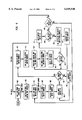
- FIG. 1 a block diagram of a switch in accordance with applicants' invention
- FIG. 2 is a block diagram of a microprocessor for use in that switch
- FIG. 3 is a layout of memory and registers used in that switch
- FIGS. 4 and 6 are flow diagrams of programs for controlling the switch.
- FIG. 5 is a block diagram of a large switch.
- FIG. 1 is a block diagram showing the input and output data streams of a time slot interchange unit in accordance with applicants' invention.
- a 100 MHz PowerPC can switch 128 serial input and output streams each consisting of 32 time slots at a bit rate of 2.048 Mbits per second.
- the input comprises n serial input streams, stream zero being connected to input buffer 101, . . . , and serial input stream n minus one being connected to input buffer 102.
- the first input stream is collected in a shift register of input buffer 101 and then transmitted in parallel sequentially to a four stage, sixty-four bit per stage, buffer.
- the last stage of this buffer is connected to a series of sixty-four tri-state bus drivers for driving parallel bus 105.
- These output buffers also comprise four stage, sixty-four bit registers, the input stage of which is connected to sixty-four bus receivers connected to bus 105 and the output stage of which is connected to a shift register for generating a serial output stream.
- microprocessor 120 Also connected to bus 105 is microprocessor 120 which accepts inputs in bursts of 256 bits as four associated 64 bit data bus reads from each of the n input buffers 101, . . . , 102 under the control of the program stored in the microprocessor.
- the microprocessor delivers bursts of 256 bits as four associated 64 bit data bus writes to each of the n output buffers after having generated the output burst through the reading of the inputs under the control of a control map and of the program of the microprocessor.
- An I/O decoder unit 130 under the control of the microprocessor is used to gate the tri-state outputs of the input buffers onto the bus and to gate the output of the bus into the n output buffers 111, . . . , 112.
- the I/O decoder receives inputs from the microprocessor address bus.
- bus 105 Also connected to bus 105 is a memory 122 for storing infrequently used data and program text such as data required for performing tests or diagnostics, and other non-cached TSI code, and as a backup for data stored in the microprocessor cache, such as the microprocessor program text and the path memory. Also connected to bus 105 is control register 124 which interfaces with a call processing controller or other switches of the telecommunications network, receives and transmits control messages.
- FIG. 2 is a block diagram those key parts of the microprocessor which are pertinent to the understanding of applicants' invention.
- the microprocessor contains a program cache 201 for storing the control program which controls the operations of the time slot interchange unit.
- the output of the program cache goes to an instruction queue 203 for storing a plurality of instructions in order to allow for the rapid execution of simple loops that is made possible using pipelining techniques.
- the instruction queue interacts with an instruction control block 205 to deliver the appropriate instructions to arithmetic and logic unit (ALU) 207.
- ALU executes its received instructions and operates to perform the steps required by the instruction by controlling load store unit 213 which in turn accesses a data cache 211.
- ALU 207 also controls a group of internal registers 215 for short term storage and for the control of the microprocessor.
- a bus interface 217 communicates with the data cache 211, and, for changes in the software, also communicates with program cache 201.
- FIG. 3 shows pertinent memory data stored in data cache 211 of microprocessor 120.
- the contents of the data cache are expanded in FIG. 3 and contain, among other items, the data received from input buffers 101, . . . , 102 and the data to be delivered to output buffers 111, . . . , 112.
- Data received from the input buffers 101, . . . , 102 is stored in TSI buffer 301 or 303.
- the data from the various input buffers is stored sequentially in one of these buffers in applicants' preferred embodiment.
- the TSI buffer contains buffer 301 and a second buffer 303 for storing another frame of this serial input data. Buffers 301 and 303 are used alternately.
- Control map 311 is used to control the reading of the contents of TSI buffers 301 or 303 in order to generate an output for storage in the TSI output buffer 321 for transmission to one of the output buffers 111, . . . , 112.
- TSI write pointer 315 is used to keep track of where the next input from one of the input buffers 101, . . . , 102 is to be stored in TSI buffer 301 or 303.
- control pointer 313 is used to point to the appropriate portion of control map 311 in order to control accessing the TSI buffer in order to obtain the time slots that are required to fill the TSI output buffer 321.
- Input buffer count 331 is used to control the cycling for accepting inputs from the appropriate one of the n input buffers 101, . . . , 102, selected by input buffer address register 332, and output buffer count 333 is used to control the distribution of an output collected in TSI output buffer 321 to one of the n output buffers 111, . . . , 112 selected by output buffer address register 334.
- Link status memory 341 is used to identify any of the n input links or any of the n output links that are out of service. This status can be checked prior to accepting an input from one of the n input buffers 101, . . . , 102 or prior to sending an output to one of the output buffers 111, . . . , 112.
- the control map is altered under the control of the program of the microprocessor when the microprocessor receives a control message from connect request register 351 within the control register 124 of FIG. 1, the control message representing a request to establish or disconnect a connection in the time slot interchange unit.
- the process of controlling the control map is well known in the prior art.
- FIG. 4 is a flow diagram describing the operation of the program for implementing a time slot interchange (TSI) in accordance with applicants' invention.
- the process starts with the microprocessor waiting for a frame synchronization pulse (block 401) .
- the frame synchronization pulse arrives, it signals the beginning of the synchronized loading of the input buffers 101, . . . , 102 from the serial input streams and triggers several initialization steps.
- the memory write address which is the TSI write pointer 315, is initialized (action block 402) so that the correct location in the TSI buffer 301 and 303 is established for writing the information from the input buffers 101, . . . , 102.
- the double buffering offset is toggled (action block 403) to choose either frame memory 301 or 303 in the TSI buffer for storing the input data on alternate frames.
- the microprocessor then waits for an input buffer loaded signal (action block 404), which establishes that the buffers 101, . . . 102 are full, and then the input buffer address is initialized (action block 405) to point to the first input buffer 101.
- action block 406 invalidates the cache data associated with the input buffer address before initiating the read.
- the input buffer pointed to by the input buffer address is then read (action block 406) in a burst as four connected 64 bit data bus operations and stored in the microprocessor cache memory in either TSI buffer 301 or 303 depending on the double buffering offset.
- Test 407 determines whether all inputs for this frame have been written. If not, then the buffer address is incremented (action block 409) and the next buffer is read into the TSI buffer (action block 406 previously described). This loop is continued until the results of test 407 indicates that all inputs for this frame have been written.
- the output buffer address 334 is initialized (action block 421), the TSI output buffer address is initialized (action 423) and the control map pointer 313 is initialized to point to the top of the control map (action block 425).
- the contents of the control map are read to an index register (action block 427) and the index register is used to read the eight bit time slot from the TSI buffer (action block 429) (frame 301 or 303 is accessed depending on the double buffering offset established in action block 403).
- the read byte is then written into the TSI output buffer in the cache, at the appropriate offset (TSI output buffer 321) (action block 431) determined by which of the 32 bytes is being written.
- Test 433 is used to determine whether 32 bytes have been written; if not, action block 427 is re-entered and the loop repeats action blocks 427, 429, 431.
- action block 427 is re-entered and the loop repeats action blocks 427, 429, 431.
- 32 bytes are written from the cache (action block 441) by a data cache block flush operation in a burst of four connected 64 bit data bus writes into the output buffer 111, . . . , 112 specified by the output buffer address 334.
- Test 443 determines whether all outputs have been written. If not, then the TSI output buffer read address is re-initialized (action block 445).
- output buffer address (output buffer address 334) is then incremented (action block 447), and the loop for writing into the output buffer is re-entered in action block 427. If test 443 indicates that all outputs have been written then the work for this frame is finished and the processor goes back to block 401 to wait for the next frame synchronization pulse.
- the above flow chart describes an eight bit time slot where a byte quantity is read and written in action blocks 429 and 431. Sixteen and 32 bit time slots could easily be accommodated with a straightforward substitution of half word or full word microprocessor instructions for the corresponding load and store byte instructions.
- the time slot width can be further generalized to include group switching where contiguous time slots are switched as a group using load/store string instructions in an action blocks 429 and 431 to transfer a sequence of time slots.
- the total number of bytes of switched information per unit of time increases with increasing time slot width or group size, since the loop overhead of action blocks 427 through 433 is reduced proportionally relative to that of a byte wide time slot. This is very efficient for switching a 32 time slot PCM (E1) facility for implementing a crossconnect.
- Groups can be concatenated contiguously to form higher bandwidth rates such as DS3 at the output of the output buffers; this is especially useful for performing the function of a digital access and cross connect switch such as the DACS-4 switch manufactured by Lucent Technologies Inc.
- the above flow chart provides double buffering for all time slots whether they represent nx64 kilobits per second signals or a single 64 kilobit per second voice or data time slot. If the additional frame delay introduced by the double buffering is not desired for the single 64 kbit/sec voice or data time slot, then the flow chart can be modified to provide selective double buffering, i.e., the single voice or data time slot is not double buffered.
- Such single buffered time slots are marked in the control map 311, which causes the time slot to be read from the other one of the two TSI buffer frames 301 and 303, by negating the effect of the double buffer offset. Thus, single buffered time slots are read out of the opposite frame from the double buffered time slots.
- the flow chart shown in FIG. 4 is transversed only once per frame because each of the serial input streams was assumed to consist of 32 time slots, which in the present implementation is written into the microprocessor cache in a single 32 byte burst, as described when action block 406 was discussed.
- FIG. 5 illustrates an arrangement for increasing the size of the TSI of FIG. 1.
- FIG. 5 shows an implementation that can be applied to any number n of input signals, any number k of microprocessor complexes and any number n over k, that can be accommodated by the speed and memory capacity of these complexes.
- n is 32
- k is 8
- n over k is 4.
- Each of the input streams, terminated at the buffer amplifiers 521-1, . . . , 521-32 is connected to a shift register input buffer similar to the input buffer 101.
- microprocessor complex 501-1 accepts inputs.
- the same arrangement is available for each of the 7 other microprocessor complexes 501-2, . . . , 501-8.
- Each microprocessor complex feeds only four of the total 32 output buffers.
- microprocessor complex 501 feeds output buffers 531-1, . . . , 531-4.
- the capacity of each microprocessor complex must be adequate to take inputs from the full range of input shift registers, but need only drive 1 over k of the output streams. Fortunately, the absorption of the inputs is done in parallel since input signals are loaded into sequential locations in the TSI buffer 301, 303 of each microprocessor. Thus, very large amounts of input data can be absorbed per unit time in the microprocessor caches. It is only the output data which requires sequential time slot by time slot or group by group processing by the microprocessor.
- the arrangement of local shift registers per microprocessor complex has the advantage of limiting high bandwidth connections to the nearby locality of each microprocessor, with the corresponding disadvantage of requiring replicated shift registers for each microprocessor.
- a single global set of shift registers could be used, with each microprocessor in lockstep, absorbing the same input data at the same time. In this case the complexity of high bandwidth global connections and global microprocessor synchronization would be traded against the savings of a set of shift registers for all but one of the microprocessors.
- TMS Time Multiplexed Switch
- the RISC microprocessor hardware of FIG. 1, the block diagram of FIG. 2 and the programmer data model of FIG. 3 can also be used for implementing a TMS.
- the basic difference is that a TSI application requires the storing and maintaining in memory of either one or two frames of time slots (single or double buffered applications), whereas a TMS application requires the switching of the time slots as soon as possible after they appear at the input to the TMS.
- FIG. 6 is a flow chart for implementing a TMS. It is very similar to the TSI basic flow chart (FIG. 4) and incorporates the changes described earlier for generalized TSI flow, as well as the differences described above for a TMS. To help the reader, the same action is given the same number as in FIG. 4. For a TMS high bandwidth facilities much larger than the 2.048 Mbits per second assumed for the basic TSI flow chart are required. This requires the addition of test 449 in FIG. 6 in order to handle the entire frame, and moving the initialize read control pointer action block (425) from the TSI read cycle to the frame initialization portion near the beginning of TMS write cycle of FIG. 6. These two steps are the same as those described for a generalized TSI flow.
- Eliminate action block 403 which is used to implement double buffering.
- the TMS flow chart of FIG. 6 implements the time multiplexed switching function.
- a variation on writing the input buffers 101, . . . , 102 sequentially into cache is that rather than take a 32 byte burst from a single input buffer, 8 bytes from each of four input buffers can be written. This has the advantage of reducing the number of bytes of buffering required by input buffers 101, . . . , 102 from 32 bytes to 8 bytes per buffer. Taking 16 bytes from each of two buffers can also be implemented.
- FIG. 5 does not work satisfactorily for broadcasting in the non-preferred arrangement (storage based on control memory and sequential readout), because for each input word that is received, different microprocessors may be required to do different amounts of processing.
Landscapes
- Engineering & Computer Science (AREA)
- Computer Networks & Wireless Communication (AREA)
- Time-Division Multiplex Systems (AREA)
- Exchange Systems With Centralized Control (AREA)
- Use Of Switch Circuits For Exchanges And Methods Of Control Of Multiplex Exchanges (AREA)
- Data Exchanges In Wide-Area Networks (AREA)
Priority Applications (6)
| Application Number | Priority Date | Filing Date | Title |
|---|---|---|---|
| US08/856,842 US6049540A (en) | 1997-05-15 | 1997-05-15 | Enhanced telecommunications switching unit |
| CA002233341A CA2233341C (en) | 1997-05-15 | 1998-03-30 | Enhanced telecommunications switching unit |
| DE69833300T DE69833300T2 (de) | 1997-05-15 | 1998-05-05 | Zeitmultiplexvermittlungseinheit |
| EP98303486A EP0878979B1 (de) | 1997-05-15 | 1998-05-05 | Zeitmultiplexvermittlungseinheit |
| JP13289598A JP3961666B2 (ja) | 1997-05-15 | 1998-05-15 | 通信交換機 |
| KR1019980017472A KR100310096B1 (ko) | 1997-05-15 | 1998-05-15 | 원거리통신회로스위치 |
Applications Claiming Priority (1)
| Application Number | Priority Date | Filing Date | Title |
|---|---|---|---|
| US08/856,842 US6049540A (en) | 1997-05-15 | 1997-05-15 | Enhanced telecommunications switching unit |
Publications (1)
| Publication Number | Publication Date |
|---|---|
| US6049540A true US6049540A (en) | 2000-04-11 |
Family
ID=25324631
Family Applications (1)
| Application Number | Title | Priority Date | Filing Date |
|---|---|---|---|
| US08/856,842 Expired - Fee Related US6049540A (en) | 1997-05-15 | 1997-05-15 | Enhanced telecommunications switching unit |
Country Status (6)
| Country | Link |
|---|---|
| US (1) | US6049540A (de) |
| EP (1) | EP0878979B1 (de) |
| JP (1) | JP3961666B2 (de) |
| KR (1) | KR100310096B1 (de) |
| CA (1) | CA2233341C (de) |
| DE (1) | DE69833300T2 (de) |
Cited By (6)
| Publication number | Priority date | Publication date | Assignee | Title |
|---|---|---|---|---|
| US6606308B1 (en) * | 1998-07-16 | 2003-08-12 | Alcatel | Method of transmitting in successive time slots |
| US6628652B1 (en) * | 1998-09-18 | 2003-09-30 | Lucent Technologies Inc. | Flexible telecommunications switching network |
| US6944153B1 (en) * | 1999-12-01 | 2005-09-13 | Cisco Technology, Inc. | Time slot interchanger (TSI) and method for a telecommunications node |
| US7260093B1 (en) | 2002-12-06 | 2007-08-21 | Integrated Device Technology, Inc. | Time-slot interchange switches having group-based output drive enable control and group-based rate matching and output enable indication capability |
| US7346048B1 (en) * | 2001-07-31 | 2008-03-18 | Lsi Logic Corporation | Efficient high density voice processor |
| US11528164B2 (en) * | 2018-11-26 | 2022-12-13 | Beckhoff Automation Gmbh | Method for operating a network subscriber and network subscriber |
Citations (4)
| Publication number | Priority date | Publication date | Assignee | Title |
|---|---|---|---|---|
| US4207435A (en) * | 1977-08-08 | 1980-06-10 | Nippon Telegraph And Telephone Public Corporation | Channel translators for use in time division digital exchangers |
| US5444700A (en) * | 1990-06-21 | 1995-08-22 | Martikainen; Olli | Switching element and method for controlling the same |
| US5546391A (en) * | 1993-03-04 | 1996-08-13 | International Business Machines Corporation | Central shared queue based time multiplexed packet switch with deadlock avoidance |
| US5557609A (en) * | 1993-12-01 | 1996-09-17 | Kabushiki Kaisha Toshiba | Switching apparatus for ATM |
Family Cites Families (2)
| Publication number | Priority date | Publication date | Assignee | Title |
|---|---|---|---|---|
| US5123012A (en) * | 1989-06-06 | 1992-06-16 | Mitsubishi Denki Kabushiki Kaisha | Time division switching apparatus |
| JP2918007B2 (ja) * | 1992-03-05 | 1999-07-12 | 日本電気株式会社 | 並列型時間スイッチ |
-
1997
- 1997-05-15 US US08/856,842 patent/US6049540A/en not_active Expired - Fee Related
-
1998
- 1998-03-30 CA CA002233341A patent/CA2233341C/en not_active Expired - Fee Related
- 1998-05-05 EP EP98303486A patent/EP0878979B1/de not_active Expired - Lifetime
- 1998-05-05 DE DE69833300T patent/DE69833300T2/de not_active Expired - Fee Related
- 1998-05-15 KR KR1019980017472A patent/KR100310096B1/ko not_active IP Right Cessation
- 1998-05-15 JP JP13289598A patent/JP3961666B2/ja not_active Expired - Fee Related
Patent Citations (4)
| Publication number | Priority date | Publication date | Assignee | Title |
|---|---|---|---|---|
| US4207435A (en) * | 1977-08-08 | 1980-06-10 | Nippon Telegraph And Telephone Public Corporation | Channel translators for use in time division digital exchangers |
| US5444700A (en) * | 1990-06-21 | 1995-08-22 | Martikainen; Olli | Switching element and method for controlling the same |
| US5546391A (en) * | 1993-03-04 | 1996-08-13 | International Business Machines Corporation | Central shared queue based time multiplexed packet switch with deadlock avoidance |
| US5557609A (en) * | 1993-12-01 | 1996-09-17 | Kabushiki Kaisha Toshiba | Switching apparatus for ATM |
Non-Patent Citations (2)
| Title |
|---|
| Alles: "An Intelligent Network Processor for a Digital Central Office"; International Zurich Seminar on Digital Communications, Paper A-5, 1978, pp. 1-6. |
| Alles: An Intelligent Network Processor for a Digital Central Office ; International Zurich Seminar on Digital Communications, Paper A 5, 1978, pp. 1 6. * |
Cited By (10)
| Publication number | Priority date | Publication date | Assignee | Title |
|---|---|---|---|---|
| US6606308B1 (en) * | 1998-07-16 | 2003-08-12 | Alcatel | Method of transmitting in successive time slots |
| US6628652B1 (en) * | 1998-09-18 | 2003-09-30 | Lucent Technologies Inc. | Flexible telecommunications switching network |
| US6944153B1 (en) * | 1999-12-01 | 2005-09-13 | Cisco Technology, Inc. | Time slot interchanger (TSI) and method for a telecommunications node |
| US7346048B1 (en) * | 2001-07-31 | 2008-03-18 | Lsi Logic Corporation | Efficient high density voice processor |
| US7633936B1 (en) | 2001-07-31 | 2009-12-15 | Lsi Corporation | Time-slot interchange circuit |
| US20100046508A1 (en) * | 2001-07-31 | 2010-02-25 | Vogel Danny C | Time-slot interchange circuit |
| US8451827B2 (en) | 2001-07-31 | 2013-05-28 | Lsi Corporation | Time-slot interchange circuit |
| US7260093B1 (en) | 2002-12-06 | 2007-08-21 | Integrated Device Technology, Inc. | Time-slot interchange switches having group-based output drive enable control and group-based rate matching and output enable indication capability |
| US7266128B1 (en) * | 2002-12-06 | 2007-09-04 | Integrated Device Technology, Inc. | Time-slot interchange switches having efficient block programming and on-chip bypass capabilities and methods of operating same |
| US11528164B2 (en) * | 2018-11-26 | 2022-12-13 | Beckhoff Automation Gmbh | Method for operating a network subscriber and network subscriber |
Also Published As
| Publication number | Publication date |
|---|---|
| KR19980087075A (ko) | 1998-12-05 |
| JPH10336775A (ja) | 1998-12-18 |
| DE69833300D1 (de) | 2006-04-13 |
| JP3961666B2 (ja) | 2007-08-22 |
| CA2233341A1 (en) | 1998-11-15 |
| DE69833300T2 (de) | 2006-08-10 |
| EP0878979A1 (de) | 1998-11-18 |
| EP0878979B1 (de) | 2006-01-25 |
| CA2233341C (en) | 2002-09-17 |
| KR100310096B1 (ko) | 2001-12-17 |
Similar Documents
| Publication | Publication Date | Title |
|---|---|---|
| EP0725555B1 (de) | Methode und Apparat zur Manipulierung einer ATM-Zelle | |
| US5559969A (en) | Method and apparatus for efficiently interfacing variable width data streams to a fixed width memory | |
| EP0725554B1 (de) | Methode und Apparat für Vermittlung, Mehrfachsendeverfahren, Multiplexierung und Demultiplexierung einer ATM-Zelle | |
| JP4480845B2 (ja) | メモリー幅の非常に広いtdmスイッチシステム | |
| US5875189A (en) | Method and apparatus for multicast of ATM cells | |
| US5261064A (en) | Burst access memory | |
| US5825770A (en) | Multiple algorithm processing on a plurality of digital signal streams via context switching | |
| US20080253404A1 (en) | Dynamic time division multiplexing circuit without a shadow table | |
| JPH10105308A (ja) | 情報伝送バス及び方法 | |
| US20010014930A1 (en) | Memory structure | |
| JP2000032064A (ja) | ネットワ―クでデ―タを転送するためのネットワ―クプロセッサシステムおよび方法 | |
| US6049540A (en) | Enhanced telecommunications switching unit | |
| KR100303970B1 (ko) | 동기식 멀티포트 인터페이스 및 그것의 인터페이스 방법 | |
| CA2151180C (en) | Method and apparatus for multicast of atm cells | |
| US5663961A (en) | Packet switch with centralized buffering for many output channels | |
| EP1031092A1 (de) | Verfahren und vorrichtung zur byteausrichtung | |
| US5883902A (en) | Time slot interchanger and digital communications terminal for ISDN D-channel assembly | |
| JPH07281950A (ja) | データ記憶装置をアクセスする方法及びメモリアクセス制御装置 | |
| US6002685A (en) | Time slot interchanger and digital communications terminal for ISDN D-channel assembly | |
| EP0710047A2 (de) | Methode und Apparat für Mehrfachsendung von ATM-Zellen | |
| JP2721458B2 (ja) | チャネル装置およびそのフレーム送受信方法 | |
| JPH06350665A (ja) | プロトコル処理装置 | |
| Fried | A VLSI chip set for burst and fast ATM switching | |
| KR100294703B1 (ko) | 비터비 디코더_ | |
| CA2223319A1 (en) | Time slot interchanger and digital communications terminal for isdn d-channel assembly |
Legal Events
| Date | Code | Title | Description |
|---|---|---|---|
| AS | Assignment |
Owner name: LUCENT TECHNOLOGIES INC., NEW JERSEY Free format text: ASSIGNMENT OF ASSIGNORS INTEREST;ASSIGNORS:CHRIN, CHRISTOPHER JAMES;ZOLA, MEYER JOSEPH;REEL/FRAME:008663/0712 Effective date: 19970515 |
|
| FEPP | Fee payment procedure |
Free format text: PAYOR NUMBER ASSIGNED (ORIGINAL EVENT CODE: ASPN); ENTITY STATUS OF PATENT OWNER: LARGE ENTITY |
|
| AS | Assignment |
Owner name: THE CHASE MANHATTAN BANK, AS COLLATERAL AGENT, TEX Free format text: CONDITIONAL ASSIGNMENT OF AND SECURITY INTEREST IN PATENT RIGHTS;ASSIGNOR:LUCENT TECHNOLOGIES INC. (DE CORPORATION);REEL/FRAME:011722/0048 Effective date: 20010222 |
|
| FEPP | Fee payment procedure |
Free format text: PAYER NUMBER DE-ASSIGNED (ORIGINAL EVENT CODE: RMPN); ENTITY STATUS OF PATENT OWNER: LARGE ENTITY Free format text: PAYOR NUMBER ASSIGNED (ORIGINAL EVENT CODE: ASPN); ENTITY STATUS OF PATENT OWNER: LARGE ENTITY |
|
| FPAY | Fee payment |
Year of fee payment: 4 |
|
| AS | Assignment |
Owner name: LUCENT TECHNOLOGIES INC., NEW JERSEY Free format text: TERMINATION AND RELEASE OF SECURITY INTEREST IN PATENT RIGHTS;ASSIGNOR:JPMORGAN CHASE BANK, N.A. (FORMERLY KNOWN AS THE CHASE MANHATTAN BANK), AS ADMINISTRATIVE AGENT;REEL/FRAME:018590/0047 Effective date: 20061130 |
|
| FPAY | Fee payment |
Year of fee payment: 8 |
|
| REMI | Maintenance fee reminder mailed | ||
| LAPS | Lapse for failure to pay maintenance fees | ||
| STCH | Information on status: patent discontinuation |
Free format text: PATENT EXPIRED DUE TO NONPAYMENT OF MAINTENANCE FEES UNDER 37 CFR 1.362 |
|
| FP | Lapsed due to failure to pay maintenance fee |
Effective date: 20120411 |