US6022767A - Semiconductor device with insulated gate electrode and method of fabricating the same - Google Patents
Semiconductor device with insulated gate electrode and method of fabricating the same Download PDFInfo
- Publication number
- US6022767A US6022767A US09/143,377 US14337798A US6022767A US 6022767 A US6022767 A US 6022767A US 14337798 A US14337798 A US 14337798A US 6022767 A US6022767 A US 6022767A
- Authority
- US
- United States
- Prior art keywords
- insulating film
- recess
- region
- forming
- film
- Prior art date
- Legal status (The legal status is an assumption and is not a legal conclusion. Google has not performed a legal analysis and makes no representation as to the accuracy of the status listed.)
- Expired - Lifetime
Links
- 239000004065 semiconductor Substances 0.000 title claims abstract description 51
- 238000004519 manufacturing process Methods 0.000 title claims abstract description 12
- 229910021420 polycrystalline silicon Inorganic materials 0.000 claims abstract description 33
- 229920005591 polysilicon Polymers 0.000 claims abstract description 33
- 239000000758 substrate Substances 0.000 claims abstract description 17
- 238000000034 method Methods 0.000 claims abstract description 15
- 238000005530 etching Methods 0.000 claims abstract description 8
- 230000001590 oxidative effect Effects 0.000 claims abstract description 5
- 229920002120 photoresistant polymer Polymers 0.000 abstract description 7
- 239000010410 layer Substances 0.000 description 40
- VYPSYNLAJGMNEJ-UHFFFAOYSA-N Silicium dioxide Chemical compound O=[Si]=O VYPSYNLAJGMNEJ-UHFFFAOYSA-N 0.000 description 20
- 238000000206 photolithography Methods 0.000 description 14
- 235000012239 silicon dioxide Nutrition 0.000 description 10
- 239000000377 silicon dioxide Substances 0.000 description 10
- 229910052581 Si3N4 Inorganic materials 0.000 description 9
- HQVNEWCFYHHQES-UHFFFAOYSA-N silicon nitride Chemical compound N12[Si]34N5[Si]62N3[Si]51N64 HQVNEWCFYHHQES-UHFFFAOYSA-N 0.000 description 9
- 238000005229 chemical vapour deposition Methods 0.000 description 7
- 238000001312 dry etching Methods 0.000 description 6
- 239000011229 interlayer Substances 0.000 description 5
- ZOXJGFHDIHLPTG-UHFFFAOYSA-N Boron Chemical compound [B] ZOXJGFHDIHLPTG-UHFFFAOYSA-N 0.000 description 4
- XAGFODPZIPBFFR-UHFFFAOYSA-N aluminium Chemical compound [Al] XAGFODPZIPBFFR-UHFFFAOYSA-N 0.000 description 4
- 229910052782 aluminium Inorganic materials 0.000 description 4
- 238000000137 annealing Methods 0.000 description 4
- 229910052785 arsenic Inorganic materials 0.000 description 4
- RQNWIZPPADIBDY-UHFFFAOYSA-N arsenic atom Chemical compound [As] RQNWIZPPADIBDY-UHFFFAOYSA-N 0.000 description 4
- 229910052796 boron Inorganic materials 0.000 description 4
- 238000009792 diffusion process Methods 0.000 description 4
- 230000003647 oxidation Effects 0.000 description 4
- 238000007254 oxidation reaction Methods 0.000 description 4
- 238000001039 wet etching Methods 0.000 description 4
- 230000015572 biosynthetic process Effects 0.000 description 2
- 238000004544 sputter deposition Methods 0.000 description 2
- 238000007796 conventional method Methods 0.000 description 1
- 230000005669 field effect Effects 0.000 description 1
- 239000012535 impurity Substances 0.000 description 1
- 230000010354 integration Effects 0.000 description 1
- 238000012986 modification Methods 0.000 description 1
- 230000004048 modification Effects 0.000 description 1
Images


Classifications
-
- H—ELECTRICITY
- H01—ELECTRIC ELEMENTS
- H01L—SEMICONDUCTOR DEVICES NOT COVERED BY CLASS H10
- H01L29/00—Semiconductor devices specially adapted for rectifying, amplifying, oscillating or switching and having potential barriers; Capacitors or resistors having potential barriers, e.g. a PN-junction depletion layer or carrier concentration layer; Details of semiconductor bodies or of electrodes thereof ; Multistep manufacturing processes therefor
- H01L29/66—Types of semiconductor device ; Multistep manufacturing processes therefor
- H01L29/68—Types of semiconductor device ; Multistep manufacturing processes therefor controllable by only the electric current supplied, or only the electric potential applied, to an electrode which does not carry the current to be rectified, amplified or switched
- H01L29/76—Unipolar devices, e.g. field effect transistors
- H01L29/772—Field effect transistors
- H01L29/78—Field effect transistors with field effect produced by an insulated gate
-
- H—ELECTRICITY
- H01—ELECTRIC ELEMENTS
- H01L—SEMICONDUCTOR DEVICES NOT COVERED BY CLASS H10
- H01L29/00—Semiconductor devices specially adapted for rectifying, amplifying, oscillating or switching and having potential barriers; Capacitors or resistors having potential barriers, e.g. a PN-junction depletion layer or carrier concentration layer; Details of semiconductor bodies or of electrodes thereof ; Multistep manufacturing processes therefor
- H01L29/40—Electrodes ; Multistep manufacturing processes therefor
- H01L29/41—Electrodes ; Multistep manufacturing processes therefor characterised by their shape, relative sizes or dispositions
- H01L29/423—Electrodes ; Multistep manufacturing processes therefor characterised by their shape, relative sizes or dispositions not carrying the current to be rectified, amplified or switched
- H01L29/42312—Gate electrodes for field effect devices
- H01L29/42316—Gate electrodes for field effect devices for field-effect transistors
- H01L29/4232—Gate electrodes for field effect devices for field-effect transistors with insulated gate
- H01L29/42364—Gate electrodes for field effect devices for field-effect transistors with insulated gate characterised by the insulating layer, e.g. thickness or uniformity
- H01L29/42368—Gate electrodes for field effect devices for field-effect transistors with insulated gate characterised by the insulating layer, e.g. thickness or uniformity the thickness being non-uniform
Definitions
- the invention relates to a semiconductor device having an insulated gate electrode, and further to a method of fabricating the same.
- FIG. 1 illustrates a conventional MOSFET formed at a surface thereof with a U-shaped recess.
- the illustrated MOSFET includes an n + semiconductor substrate 1, on which an n - epitaxial layer 2 is formed.
- the n - epitaxial layer 2 is formed at a surface thereof with a p-type base region 3, at a surface of which is formed an n + source region 4.
- the n - epitaxial layer 2 other than the p-type base region 3 constitutes a drain region 2a.
- the n - epitaxial layer 2 is formed with a U-shaped recess 5 starting from a surface of the source region 4 and reaching the drain region 2a through the base region 3.
- the recess 5 and a part of the source region 4 are covered with a gate oxide film 6, on which a gate electrode 7 is formed.
- An interlayer insulating film 8 is formed on the gate electrode 7 and the gate oxide film 6 so that the gate electrode 7 is entirely covered with the interlayer insulating film 8.
- the source region 4 and the base region 3 make electrical contact with a source electrode (not illustrated) at a surface of the base region 3 and also at a portion of a surface of the source region 4 on which the interlayer insulating film 8 is not formed.
- the n - epitaxial layer 2 is formed in the n + semiconductor substrate 1.
- a silicon dioxide film 10 is formed at a surface of the epitaxial layer 2 by thermal oxidation, and a silicon nitride film 11 is formed all over the silicon dioxide film 10 by chemical vapor deposition (CVD).
- the silicon nitride film 11 acts as a mask for preventing growth of the silicon dioxide film 10.
- the silicon nitride film 11, the silicon dioxide film 10, and the epitaxial layer 2 are etched at a selected region by photolithography and dry etching to thereby form a recess 5.
- the recess 5 is thermally oxidized to thereby form LOCOS oxide film 13 in the recess 5.
- the rectangular recess 5 is changed into a U-shaped recess.
- the silicon nitride film 11 is completely removed by wet etching.
- the semiconductor substrate 1 is ion-implanted with boron with LOCOS dioxide film 13 being used as a mask, followed by annealing for thermal diffusion of boron to thereby form the p-type base region 3 in the epitaxial layer 2.
- arsenic is ion-implanted into the base region 3 with both LOCOS dioxide film and a photoresist film (not illustrated) being used as a mask, followed by annealing for thermal diffusion of arsenic to thereby form the n + source region 4.
- the epitaxial layer 2 other than the base region 3 and the source region 4 constitutes the n - drain region 2a.
- LOCOS oxide film 13 and the silicon dioxide film 10 are removed by wet etching to thereby expose the base region 3, the source region 4, and the recess 5.
- a gate oxide film 6 is formed on both an inner wall of the recess 5 and surfaces of the base region 3 and the source region 4 by thermal oxidation.
- a polysilicon layer 15 is formed all over the epitaxial layer 2 by CVD.
- the polysilicon film 15 is patterned by photolithography and dry etching so that the polysilicon film 15 remained unetched only in the recess 5 and on a part of surface of the source region 4, to thereby form the gate electrode 7. Thereafter, the epitaxial layer 2 is covered at a surface thereof with the interlayer insulating film 8 by CVD.
- the epitaxial layer 2 is entirely covered with an aluminum film by sputtering, followed by removal of the aluminum film in a selected region by photolithography and dry etching, to thereby form a source electrode (not illustrated) which makes electrical contact with both the base region 3 and the source region 4.
- Japanese Unexamined Patent Publication No. 4-258174 published on Sep. 14, 1992 has suggested a semiconductor device including a semiconductor substrate formed at a surface thereof with a trench recess, a gate oxide film covering inner and bottom walls of the recess therewith, a first polysilicon film formed in the trench recess, and a second polysilicon film surrounded by the first polysilicon film for planarizing the trench recess, and an oxide film formed only on a gate electrode for electrically insulating the first polysilicon film from source region.
- a semiconductor device including (a) a semiconductor region formed at a surface thereof with a recess and including a drain region having a first electrical conductivity, a base region having a second electrical conductivity, and a source region having a first electrical conductivity, an interface between the drain region and the base region being at the level within a depth of the recess, and an interface between the base region and the source region being at the level within a depth of the recess, (b) a first insulating film formed on an inner wall of the recess, (c) a gate electrode formed in the recess and having a thickness smaller than a depth of the recess, and (d) a second insulating film formed on the gate electrode.
- a semiconductor device including (a) a semiconductor substrate, (b) an epitaxial layer formed on the semiconductor substrate, the epitaxial layer being formed at a surface thereof with a recess and including a drain region having a first electrical conductivity, a base region having a second electrical conductivity, and a source region having a first electrical conductivity, an interface between the drain region and the base region being at the level within a depth of the recess, and an interface between the base region and the source region being at the level within a depth of the recess, (c) a first insulating film formed on an inner wall of the recess, (d) a gate electrode formed in the recess and having a thickness smaller than a depth of the recess, and (e) a second insulating film formed on the gate electrode.
- the base region may be formed on the drain region, and the source region may be formed at a surface of the base region.
- the drain region is a lightly doped one, and the source region is a heavily doped one.
- the second insulating film is LOCOS oxide film, and has such a thickness that the second insulating film is on a level with the semiconductor region or epitaxial layer.
- the second insulating film may be employed as a mask for forming the source region, and for exposing the base region and the source region.
- the semiconductor device may further include a source electrode formed over the base region and the source region.
- the semiconductor region or substrate may be heavily doped and have a first electrical conductivity, wherein the semiconductor device constitutes MOSFET, for instance.
- the semiconductor region or substrate may be heavily doped and have a second electrical conductivity, wherein the semiconductor device constitutes MOSFET which modulates conductivity thereof, for instance.
- a method of fabricating a semiconductor device including the steps of (a) forming a first insulating film on a semiconductor region, (b) forming the semiconductor region with a recess, (c) forming a gate insulating film on an inner wall of the recess, (d) forming a polysilicon film so that the recess is filled with the polysilicon film, (e) etching back the polysilicon film so that a gate electrode having a thickness smaller than a depth of the recess is formed in the recess, (f) oxidizing the gate electrode at its surface with the first insulating film being used as a mask, to thereby form a third insulating film on the gate electrode, (g) forming a base region at a surface of the semiconductor region with the third insulating film being used as a mask so that the base region has a thickness smaller than a depth of the recess, the base region having an electrical conductivity different from that of the semiconductor region,
- a method of fabricating a semiconductor device including the steps of (a) sequentially forming an epitaxial layer and a first insulating film on a semiconductor substrate, (b) forming the epitaxial layer with a recess, (c) forming a gate insulating film on an inner wall of the recess, (d) forming a polysilicon film so that the recess is filled with the polysilicon film, (e) etching back the polysilicon film so that a gate electrode having a thickness smaller than a depth of the recess is formed in the recess, (f) oxidizing the gate electrode at its surface with the first insulating film being used as a mask, to thereby form a third insulating film on the gate electrode, (g) forming a base region at a surface of the epitaxial layer with the third insulating film being used as a mask so that the base region has a thickness smaller than a depth of the recess, the base region having an electrical conductivity different from that
- the source region is formed to be a heavily doped one in the step (h).
- the third insulating film may be formed as LOCOS oxide film. It is preferable that the third insulating film is formed in the step (f) having such a thickness that the third insulating film is on a level with the epitaxial layer. It is preferable that the polysilicon film is etched back in the step (e) so that the third insulating film formed in the step (f) could have such a thickness that the third insulating film is on a level with the epitaxial layer.
- the polysilicon film remains unetched having a certain thickness in the recess in self-aligned manner by etching back the polysilicon film.
- the present invention makes it possible to form a source region smaller in a planar size, and hence it is also possible to form a unit cell in a smaller size, which ensures greater integration of devices than conventional semiconductor devices, and reduction in on-resistance.
- FIG. 1 is a cross-sectional view of a conventional MOSFET.
- FIGS. 2A to 2C are cross-sectional views each illustrating respective step of a method of fabricating the conventional MOSFET illustrated in FIG. 1.
- FIG. 3 is a cross-sectional view of MOSFET in accordance with the preferred embodiment of the present invention.
- FIGS. 4A to 4D are cross-sectional views each illustrating respective step of a method of fabricating MOSFET illustrated in FIG. 3.
- FIG. 3 illustrates MOSFET in accordance with the preferred embodiment of the present invention.
- the illustrated MOSFET includes a semiconductor region 21a comprising a heavily doped n + semiconductor substrate 21, and an epitaxial layer 22 formed on the n + semiconductor substrate 21.
- the epitaxial layer 22 is formed at a surface thereof with a recess 25.
- the epitaxial layer 22 is formed at a surface thereof with a p-type base region 23 having a shallower junction depth than a depth of the recess 25.
- the p-type base region 23 has formed with at a surface thereof with n + source regions 24 sandwiching the recess 25 therebetween.
- the epitaxial layer 22 other than the base region 23 and the source region 24 constitutes a drain region 22a.
- a horizontally extending interface between the drain region 22a and the base region 23 is at the level within a depth of the recess 25.
- a horizontally extending interface between the base region 23 and the source region 24 is at the level within a depth of the recess 25.
- the recess 25 is covered at an inner wall thereof with a gate oxide film 26.
- a gate electrode 27 is formed in the recess 25.
- the gate electrode 27 has a thickness smaller than a depth of the recess 25.
- LOCOS oxide film 28 is formed over the gate electrode 27 so that the rest of the recess 25 is filled with LOCOS oxide film 28.
- LOCOS oxide film 28 is designed to have a surface almost on a level with a surface of the epitaxial layer 22.
- a source electrode 29 which makes electrical contact with both the source region 24 and the base region 23 at surfaces thereof.
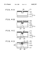
- FIG. 1 A method of fabricating the above-mentioned MOSFET illustrated in FIG. 1 is explained hereinbelow with reference to FIGS. 4A to 4D.
- the n + semiconductor substrate 21 is formed at a surface thereof with the epitaxial doped 22 containing n-type impurities at a low concentration.
- the epitaxial layer 22 is formed at a surface thereof with the silicon dioxide film 30 by thermal oxidation.
- a silicon nitride film 31 is formed all over the silicon dioxide film 10 by chemical vapor deposition (CVD).
- the silicon nitride film 31 acts as a mask for preventing growth of the silicon dioxide film 30.
- the silicon nitride film 31, the silicon dioxide film 30, and the epitaxial layer 22 are etched at a selected region by photolithography and dry etching to thereby form a recess 25 reaching an intermediate depth of the epitaxial layer 22.
- the recess 25 is thermally oxidized to thereby form a gate oxide film 26 on an inner wall of the recess 25.
- a polysilicon film 35 is formed all over the epitaxial layer 22 by CVD so that the recess 25 is filled with the polysilicon film 35.
- the polysilicon film 35 is etched back by dry etching to thereby have such a thickness that LOCOS oxide film 28 which will be formed in a later step would have a surface on a level with a surface of the epitaxial layer 22. As a result, there is formed a gate electrode 27 in the recess 25.
- the gate electrode 27 is thermally oxidized at a surface thereof with the silicon nitride film 31 being used as a mask, to thereby form LOCOS oxide film 28 at a surface of the gate electrode 27.
- the thus formed LOCOS oxide film 28 has a surface almost on a level with the epitaxial layer 22.
- an upper edge of the recess 25 is eaten away by LOCOS oxide film 28, and hence, becomes rounded.
- the silicon nitride film 31 is completely removed by wet etching.
- the epitaxial layer 22 is ion-implanted with boron with LOCOS dioxide film 28 being used as a mask, followed by annealing for thermal diffusion of boron to thereby form the p-type base region 23 in the epitaxial layer 22.
- arsenic is ion-implanted into the base region 23 with both LOCOS dioxide film 28 and a photoresist film (not illustrated) being used as a mask, followed by annealing for thermal diffusion of arsenic to thereby form the n + source region 24 in the p-type base region 23.
- the epitaxial layer 22 other than the p-type base region 23 and the n + source region 24 constitutes the n - drain region 22a.
- the silicon dioxide film 30 is removed by wet etching with LOCOS oxide film 13 being used as a mask, to thereby expose the base region 23 and the source region 24.
- the epitaxial layer 22 is entirely covered with an aluminum film by sputtering, followed by removal of the aluminum film in a selected region by photolithography and dry etching, to thereby form a source electrode 29 making electrical contact with both the base region 23 and the source region 24.
- the polysilicon film 35 remains unetched in the recess 25 in self-aligned manner, having a certain thickness smaller than a depth of the recess 25, by etching back the polysilicon film 35, when the gate electrode 27 is to be formed.
- the gate electrode 27 it is possible to form the gate electrode 27 without carrying out a photolithography step.
- the source region 24 on the thus formed gate electrode 27 with LOCOS oxide film 28, which have been formed in self-aligned fashion, being used as a mask. That is, the gate electrode 27 can be formed without carrying out a photolithography step. Hence, it is no longer necessary to have a registration margin between the source region 24 and the gate electrode 27 unlike the conventional method mentioned earlier.
- the source region 24 and the base region 23 may be formed prior to the formation of the recess 25.
- the source region 24 having a shallow junction depth it would be quite difficult to control a junction depth of the source region 24 because of a thermal oxidation step to be carried out later for forming LOCOS oxide film 28.
- the semiconductor region 21a is comprised of the semiconductor substrate 21 and the epitaxial layer 22. However, it should be noted that the semiconductor region 21a might be comprised only of the semiconductor region 21.
- the semiconductor substrate 21 is designed to be heavily doped and have an n-type conductivity.
- the semiconductor substrate 21 may be designed to have a p-type conductivity, in which case, the semiconductor device constitutes MOSFET which can modulate conductivity thereof.
- n- and p-type conductivity mentioned in the above-mentioned embodiment may be changed into p- and n-type, respectively.
Landscapes
- Engineering & Computer Science (AREA)
- Microelectronics & Electronic Packaging (AREA)
- Power Engineering (AREA)
- Physics & Mathematics (AREA)
- Ceramic Engineering (AREA)
- Condensed Matter Physics & Semiconductors (AREA)
- General Physics & Mathematics (AREA)
- Computer Hardware Design (AREA)
- Insulated Gate Type Field-Effect Transistor (AREA)
- Element Separation (AREA)
Abstract
Description
Claims (10)
Applications Claiming Priority (2)
| Application Number | Priority Date | Filing Date | Title |
|---|---|---|---|
| JP9231888A JPH1174513A (en) | 1997-08-28 | 1997-08-28 | Semiconductor of insulating gate type and its manufacture |
| JP9-231888 | 1997-08-28 |
Publications (1)
| Publication Number | Publication Date |
|---|---|
| US6022767A true US6022767A (en) | 2000-02-08 |
Family
ID=16930611
Family Applications (1)
| Application Number | Title | Priority Date | Filing Date |
|---|---|---|---|
| US09/143,377 Expired - Lifetime US6022767A (en) | 1997-08-28 | 1998-08-28 | Semiconductor device with insulated gate electrode and method of fabricating the same |
Country Status (4)
| Country | Link |
|---|---|
| US (1) | US6022767A (en) |
| JP (1) | JPH1174513A (en) |
| CN (1) | CN1118101C (en) |
| TW (1) | TW437089B (en) |
Cited By (1)
| Publication number | Priority date | Publication date | Assignee | Title |
|---|---|---|---|---|
| US6194273B1 (en) * | 1998-03-25 | 2001-02-27 | Nec Corporation | Method of manufacturing an insulated gate type semiconductor device having a U-shaped groove |
Families Citing this family (2)
| Publication number | Priority date | Publication date | Assignee | Title |
|---|---|---|---|---|
| KR100562309B1 (en) | 2004-12-29 | 2006-03-22 | 동부아남반도체 주식회사 | Transistor having reverse spacer and fabrication method thereof |
| CN110729231A (en) * | 2018-07-17 | 2020-01-24 | 中芯国际集成电路制造(上海)有限公司 | Method for manufacturing semiconductor device and semiconductor device |
Citations (4)
| Publication number | Priority date | Publication date | Assignee | Title |
|---|---|---|---|---|
| US5034785A (en) * | 1986-03-24 | 1991-07-23 | Siliconix Incorporated | Planar vertical channel DMOS structure |
| US5298780A (en) * | 1992-02-17 | 1994-03-29 | Mitsubishi Denki Kabushiki Kaisha | Semiconductor device and method of fabricating same |
| US5719409A (en) * | 1996-06-06 | 1998-02-17 | Cree Research, Inc. | Silicon carbide metal-insulator semiconductor field effect transistor |
| US5770878A (en) * | 1996-04-10 | 1998-06-23 | Harris Corporation | Trench MOS gate device |
-
1997
- 1997-08-28 JP JP9231888A patent/JPH1174513A/en active Pending
-
1998
- 1998-08-21 TW TW087113866A patent/TW437089B/en not_active IP Right Cessation
- 1998-08-27 CN CN98117398A patent/CN1118101C/en not_active Expired - Fee Related
- 1998-08-28 US US09/143,377 patent/US6022767A/en not_active Expired - Lifetime
Patent Citations (4)
| Publication number | Priority date | Publication date | Assignee | Title |
|---|---|---|---|---|
| US5034785A (en) * | 1986-03-24 | 1991-07-23 | Siliconix Incorporated | Planar vertical channel DMOS structure |
| US5298780A (en) * | 1992-02-17 | 1994-03-29 | Mitsubishi Denki Kabushiki Kaisha | Semiconductor device and method of fabricating same |
| US5770878A (en) * | 1996-04-10 | 1998-06-23 | Harris Corporation | Trench MOS gate device |
| US5719409A (en) * | 1996-06-06 | 1998-02-17 | Cree Research, Inc. | Silicon carbide metal-insulator semiconductor field effect transistor |
Cited By (1)
| Publication number | Priority date | Publication date | Assignee | Title |
|---|---|---|---|---|
| US6194273B1 (en) * | 1998-03-25 | 2001-02-27 | Nec Corporation | Method of manufacturing an insulated gate type semiconductor device having a U-shaped groove |
Also Published As
| Publication number | Publication date |
|---|---|
| TW437089B (en) | 2001-05-28 |
| JPH1174513A (en) | 1999-03-16 |
| CN1118101C (en) | 2003-08-13 |
| CN1210370A (en) | 1999-03-10 |
Similar Documents
| Publication | Publication Date | Title |
|---|---|---|
| KR100400079B1 (en) | Method for fabricating trench-gated power semiconductor device | |
| JP3157357B2 (en) | Semiconductor device | |
| US6545317B2 (en) | Semiconductor device having a gate electrode with a sidewall insulating film and manufacturing method thereof | |
| JPH09129868A (en) | Semiconductor device and its manufacture | |
| US6022767A (en) | Semiconductor device with insulated gate electrode and method of fabricating the same | |
| JPH07273330A (en) | Semiconductor device and its manufacture | |
| US6104069A (en) | Semiconductor device having an elevated active region formed in an oxide trench | |
| KR100234692B1 (en) | Transistor and the manufacturing method thereof | |
| JP3225368B2 (en) | Semiconductor device | |
| JP3038740B2 (en) | Method for manufacturing semiconductor device | |
| KR100240683B1 (en) | Method for manufacturing semiconductor device | |
| KR980012599A (en) | Methods of forming transistors using salicide process technology | |
| JPH0491481A (en) | Mis field effect transistor | |
| KR100269628B1 (en) | A method of fabricating semiconductor device | |
| JP2990029B2 (en) | Method of manufacturing complementary MISFET | |
| JPH06204472A (en) | Manufacture of trench-type source/ drain mosfet | |
| KR100202194B1 (en) | Method of manufacturing semiconductor device | |
| KR100216320B1 (en) | Method for fabricating mosfet | |
| JPH11307767A (en) | Insulation gate type semiconductor device | |
| JP2005019584A (en) | Semiconductor device and its manufacturing method | |
| JPH0888268A (en) | Manufacture of semiconductor device | |
| JP2002076341A (en) | Semiconductor device and its manufacturing method | |
| KR19990074704A (en) | Manufacturing Method of Semiconductor Device | |
| JPH06334180A (en) | Insulation gate type transistor | |
| JPH07105401B2 (en) | Semiconductor device and manufacturing method thereof |
Legal Events
| Date | Code | Title | Description |
|---|---|---|---|
| AS | Assignment |
Owner name: NEC CORPORATION, JAPAN Free format text: ASSIGNMENT OF ASSIGNORS INTEREST;ASSIGNOR:YAMAGISHI, KAZUO;REEL/FRAME:009422/0687 Effective date: 19980814 |
|
| FEPP | Fee payment procedure |
Free format text: PAYOR NUMBER ASSIGNED (ORIGINAL EVENT CODE: ASPN); ENTITY STATUS OF PATENT OWNER: LARGE ENTITY |
|
| STCF | Information on status: patent grant |
Free format text: PATENTED CASE |
|
| AS | Assignment |
Owner name: NEC ELECTRONICS CORPORATION, JAPAN Free format text: ASSIGNMENT OF ASSIGNORS INTEREST;ASSIGNOR:NEC CORPORATION;REEL/FRAME:013755/0392 Effective date: 20021101 |
|
| AS | Assignment |
Owner name: NEC ELECTRONICS CORPORATION, JAPAN Free format text: ASSIGNMENT OF ASSIGNORS INTEREST;ASSIGNOR:NEC CORPORATION;REEL/FRAME:013751/0721 Effective date: 20021101 |
|
| FPAY | Fee payment |
Year of fee payment: 4 |
|
| FPAY | Fee payment |
Year of fee payment: 8 |
|
| AS | Assignment |
Owner name: RENESAS ELECTRONICS CORPORATION, JAPAN Free format text: CHANGE OF NAME;ASSIGNOR:NEC ELECTRONICS CORPORATION;REEL/FRAME:025185/0597 Effective date: 20100401 |
|
| FPAY | Fee payment |
Year of fee payment: 12 |
|
| AS | Assignment |
Owner name: RENESAS ELECTRONICS CORPORATION, JAPAN Free format text: CHANGE OF ADDRESS;ASSIGNOR:RENESAS ELECTRONICS CORPORATION;REEL/FRAME:044928/0001 Effective date: 20150806 |