US5949223A - Power source apparatus having first and second switching power source units - Google Patents
Power source apparatus having first and second switching power source units Download PDFInfo
- Publication number
- US5949223A US5949223A US08/812,156 US81215697A US5949223A US 5949223 A US5949223 A US 5949223A US 81215697 A US81215697 A US 81215697A US 5949223 A US5949223 A US 5949223A
- Authority
- US
- United States
- Prior art keywords
- power source
- output
- switching
- current
- circuit
- Prior art date
- Legal status (The legal status is an assumption and is not a legal conclusion. Google has not performed a legal analysis and makes no representation as to the accuracy of the status listed.)
- Expired - Lifetime
Links
Images


Classifications
-
- H—ELECTRICITY
- H02—GENERATION; CONVERSION OR DISTRIBUTION OF ELECTRIC POWER
- H02M—APPARATUS FOR CONVERSION BETWEEN AC AND AC, BETWEEN AC AND DC, OR BETWEEN DC AND DC, AND FOR USE WITH MAINS OR SIMILAR POWER SUPPLY SYSTEMS; CONVERSION OF DC OR AC INPUT POWER INTO SURGE OUTPUT POWER; CONTROL OR REGULATION THEREOF
- H02M3/00—Conversion of dc power input into dc power output
- H02M3/02—Conversion of dc power input into dc power output without intermediate conversion into ac
- H02M3/04—Conversion of dc power input into dc power output without intermediate conversion into ac by static converters
- H02M3/10—Conversion of dc power input into dc power output without intermediate conversion into ac by static converters using discharge tubes with control electrode or semiconductor devices with control electrode
- H02M3/145—Conversion of dc power input into dc power output without intermediate conversion into ac by static converters using discharge tubes with control electrode or semiconductor devices with control electrode using devices of a triode or transistor type requiring continuous application of a control signal
- H02M3/155—Conversion of dc power input into dc power output without intermediate conversion into ac by static converters using discharge tubes with control electrode or semiconductor devices with control electrode using devices of a triode or transistor type requiring continuous application of a control signal using semiconductor devices only
- H02M3/156—Conversion of dc power input into dc power output without intermediate conversion into ac by static converters using discharge tubes with control electrode or semiconductor devices with control electrode using devices of a triode or transistor type requiring continuous application of a control signal using semiconductor devices only with automatic control of output voltage or current, e.g. switching regulators
- H02M3/158—Conversion of dc power input into dc power output without intermediate conversion into ac by static converters using discharge tubes with control electrode or semiconductor devices with control electrode using devices of a triode or transistor type requiring continuous application of a control signal using semiconductor devices only with automatic control of output voltage or current, e.g. switching regulators including plural semiconductor devices as final control devices for a single load
-
- H—ELECTRICITY
- H02—GENERATION; CONVERSION OR DISTRIBUTION OF ELECTRIC POWER
- H02M—APPARATUS FOR CONVERSION BETWEEN AC AND AC, BETWEEN AC AND DC, OR BETWEEN DC AND DC, AND FOR USE WITH MAINS OR SIMILAR POWER SUPPLY SYSTEMS; CONVERSION OF DC OR AC INPUT POWER INTO SURGE OUTPUT POWER; CONTROL OR REGULATION THEREOF
- H02M1/00—Details of apparatus for conversion
- H02M1/0067—Converter structures employing plural converter units, other than for parallel operation of the units on a single load
- H02M1/007—Plural converter units in cascade
Definitions
- the invention relates to a switching power source apparatus for controlling an output voltage to a constant voltage by switching an input power source and, more particularly, to a switching power source apparatus which is used for a load such as to temporarily request a large peak current for a stationary output current.
- FIG. 5 is a block diagram showing a construction of a conventional switching power source apparatus of a step-down chopper type.
- reference numerals 501 and 502 denote input terminals.
- a DC power source Vin is connected between the input terminals 501 and 502 and a DC voltage is supplied.
- Reference numerals 503 and 504 denote output terminals.
- a load 505 is connected between the output terminals 503 and 504.
- Q5 denotes a switching transistor in which a collector is connected to one input terminal 501, an emitter is connected to one terminal of a choke coil L5 and a cathode of a diode D5, and a base is connected to a control circuit 506.
- Another terminal of the choke coil L5 is connected to one terminal of a current detecting resistor R5 and a current detecting circuit 507. Another terminal of the resistor R5 is connected to the plus side of a smoothing capacitor C5, the current detecting circuit 507, a voltage detecting circuit 508, and one output terminal 503. An output of the current detecting circuit 507 connected between the current detecting resistor R5 and an output of the voltage detecting circuit 508 connected to one output terminal 503 are connected to the control circuit 506.
- the other input terminal 502, the other output terminal 504, an anode side of the diode D5, and a cathode side of the smoothing capacitor C5 are commonly connected to the ground.
- a PWM (pulse width modulation) control is executed by the control circuit 506 on the basis of outputs of the current detecting circuit 507 and voltage detecting circuit 508 and a pulse which is pulse width modulated is supplied to the base of the switching transistor Q5.
- the switching transistor Q5 is turned on/off. For a period of time during which the switching transistor Q5 is ON, energy is supplied to the choke coil L5, smoothing capacitor C5, and load 505. Since current flows, the energy is accumulated in the choke coil L5. In this instance, the diode D5 is OFF.
- the current detecting circuit 507 detects the current flowing in the current detecting resistor R5 and generates a signal to the control circuit 506.
- the voltage detecting circuit 508 detects the voltage (output voltage) at one output terminal 503 and generates a signal to the control circuit 506.
- the control circuit 506 changes a duty ratio of the pulse which is supplied to the base of the switching transistor Q5 so that an output voltage is made constant by a signal from the voltage detecting circuit 508.
- the control circuit 506 stops the operation of the switching transistor Q5, thereby keeping the output voltage constant and protecting the apparatus from the overcurrent and overvoltage.
- a set value to protect against the overcurrent has to be set to a slightly large value so as to correspond to a peak output current.
- the load 505 in FIG. 5 is, for example, a motor which is used for a paper feed in a copying apparatus or the like such that a sudden rotation is performed after a stop period or a sudden rotation and a stop are repeatedly carried out or, even if the motor is not a paper feed motor, when the motor is suddenly rotated as in a case where a rotational speed suddenly rises from a constant rotating state or the like, a very large peak current is requested for a stationary current (current when the motor is stopped or when it is rotated at a constant speed).
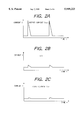
- a current as shown in an output current Iout in FIG. 6A is requested in the load (when the motor load is activated from a stop state, an output current suddenly increases and a peak current flows).
- Input/output power in FIG. 5 will now be considered. Since the output power suddenly increases, the input power also obviously suddenly increases. In this instance, a peak current such as input current Iin in FIG. 6B also flows to the input side of the switching power source apparatus.
- the conventional switching power source apparatus when a sudden peak current is requested in the load (for example, at the time of an activation of the motor load or the like), since a large current also flows to the input side of the switching power source apparatus, as an input power source, a transformer, and circuit elements of the switching power source apparatus, those having large capacities have to be used so that they can cope with the peak current. There is a problem such that the output voltage drops when a temporary abnormality of the input power source (voltage drop, power supply interruption, or the like) occurs.
- Another object of the invention is to provide a switching power source apparatus which can reduce capacities of an input power source and each element and can obtain a stable output even if a temporary abnormality of the input power source occurs.
- FIG. 1 is a block diagram showing a construction of a switching power source apparatus according to the first embodiment of the invention
- FIGS. 2A, 2B and 2C are diagrams showing current waveforms of respective portions of the switching power source apparatus
- FIG. 3 is a block diagram showing a construction of a switching power source apparatus according to the second embodiment of the invention.
- FIG. 4 is a block diagram showing a construction of a switching power source apparatus according to the third embodiment of the invention.
- FIG. 5 is a block diagram showing a construction of a conventional switching power source apparatus.
- FIGS. 6A and 6B are diagrams showing current waveforms of respective portions of the conventional switching power source apparatus.
- FIG. 1 is a block diagram showing a construction of a switching power source apparatus of a step-up/down type chopper according to the first embodiment of the invention.
- reference numeral 1 denotes a first switching power source unit and 2 indicates a second switching power source unit.
- the first switching power source unit 1 has input terminals 3 and 4 and output terminals 5 and 6.
- the DC power source Vin is connected between the input terminals 3 and 4 for supplying DC voltage.
- a large capacity power accumulating and smoothing capacitor C1 is connected between the output terminals 5 and 6.
- the first switching power source unit 1 has a switching transistor Q1 in which a collector is connected to one input terminal 3, an emitter is connected to one terminal of a choke coil L1 and a cathode of a diode D1, and a base is connected to a control circuit 7.
- Another terminal of the choke coil L1 is connected to one terminal of a current detecting resistor R1 and a current detecting circuit 8. Another terminal of the resistor R1 is connected to a plus side of the power accumulating and smoothing capacitor C1, the current detecting circuit 8, a voltage detecting circuit 9, and the output terminal 5. An output of the current detecting circuit 8 connected across the current detecting resistor R1 and an output of the voltage detecting circuit 9 connected to the output terminals 5 and 6 are connected to the control circuit 7.
- the 5 other input terminal 4, the other output terminal 6, an anode side of the diode D1, and a cathode side of the power accumulating and smoothing capacitor C1 are commonly connected to ground.
- Input terminals of the second switching power source unit 2 are connected to the output terminals 5 and 6 of the first switching power source unit 1.
- the second switching power source unit 2 has output terminals 10 and 11.
- a load 12 is connected between the output terminals 10 and 11.
- the circuit of FIG. 1 is constructed by: the first switching power source unit 1 in which the terminals 3 and 4 are set to inputs and the terminals 5 and 6 are set to outputs; the second switching power source unit 2 in which the terminals 5 and 6 are set to inputs and the terminals 10 and 11 are set to outputs; and the power accumulating and smoothing capacitor C1.
- a switching power source apparatus of a step-up/down type chopper is formed.
- a positive polarity side of the power accumulating and smoothing capacitor C1 is connected to a collector of a switching transistor Q2 through a choke coil L2 and is also connected to an anode side of a diode D2.
- a cathode side of the diode D2 is connected to a smoothing capacitor C2, the output terminal 10, and the load 12.
- An emitter of the switching transistor Q2 is connected to ground through a current detecting resistor R2.
- a current detecting circuit 15 is connected across the current detecting resistor R2 and an output signal from current detecting circuit 15 is inputted to a control circuit 14.
- a voltage detecting circuit 16 is connected between the output terminals 10 and 11 and its output is inputted to the control circuit 14.
- the input terminal 4, the output terminal 11, the anode side of the diode D1, the minus side of the smoothing capacitor C2, the minus side of the power accumulating and smoothing capacitor C1, and one end of the current detecting resistor R2 are commonly connected to ground.
- the switching transistor Q1 When a DC power source is supplied from the input terminals 3 and 4, on the basis of detection values of the current detecting circuit 8 and voltage detecting circuit 9, the switching transistor Q1 is turned on/off by the control circuit 7 so that the output current and output voltage in the first switching power source unit 1 are set to certain predetermined values. For a period of time during which the switching transistor Q1 is ON, energy is supplied to the choke coil L1, power accumulating and smoothing capacitor C1, and second switching power source unit 2. Since current flows, energy is accumulated in the choke coil L1. At this time, the diode D1 is OFF. When the switching transistor Q1 is turned off, energy accumulated in the choke coil L1 is supplied to the second switching power source unit 2 through the diode D1.
- the current detecting circuit 8 detects the current flowing in the resistor R1 and generates a detection signal to the control circuit 7.
- the voltage detecting circuit 9 detects the voltage (output voltage of the first switching power source unit 1) at the output terminal 5 and generates a detection signal to the control circuit 7.
- the control circuit 7 changes a duty ratio of a driving pulse which is supplied to the base of the switching transistor Q1 so that the current flowing in the resistor R1 and the voltage between the output terminals 5 and 6 are set to certain predetermined values, namely, the output of the first switching power source unit 1 is set to a constant voltage and constant current output, thereby on/off controlling the switching transistor Q1.
- a protection to stop the operation of the switching transistor Q1 is performed against an overcurrent and an overvoltage in the first switching power source unit 1.
- a set value to protect from the overcurrent is set to a slightly low value, thereby suppressing peak current flow in the input current of the first switching power source unit 1.
- the DC power derived between the output terminals 5 and 6 as mentioned above is supplied to the second switching power source unit 2.
- the switching transistor Q2 is turned on/off by the control circuit 14 so that the output voltage is set to a predetermined value. For a period of time during which the switching transistor Q2 is ON, current flows in the choke coil L2. In this instance, since current flows, energy is accumulated in the choke coil L2.
- the switching transistor Q2 When the switching transistor Q2 is turned off, the energy accumulated in choke coil L2 passes through the diode D2 and is supplied to the load 12 connected to the output terminals 10 and 11. In this instance, the voltage between the output terminals 10 and 11 is set to a voltage in which a counter electromotive force of the choke coil L2 is added to the voltage between the output terminals 5 and 6 (output voltage of the first switching power source unit 1).
- the current detecting circuit 15 detects the current flowing in the current detecting resistor R2 and generates a detection signal to the control circuit 14.
- the voltage detecting circuit 16 detects the voltage (output voltage) between the output terminals 10 and 11 and generates a detection signal which is provided to the control circuit 14.
- the control circuit 14 On the basis of the signals from the current detecting circuit 15 and voltage detecting circuit 16, the control circuit 14 on/off controls the switching transistor Q2 so that the voltage between the output terminals 10 and 11 is set to a predetermined value.
- the second switching power source unit 2 constant voltage controls the output voltage.
- the overcurrent and overvoltage in the second switching power source unit 2 are detected by the current detecting circuit 15 and voltage detecting circuit 16, by stopping the operation of the switching transistor Q2 or by another method, the circuit is protected.
- the load 12 in FIG. 1 is a load such as a motor which is used for a paper feed in a copying apparatus or the like such that a sudden rotation is performed after a stop period or a sudden rotation and a stop are repeatedly carried out or, even if the motor is not a paper feed motor, when the motor is suddenly rotated as in a case where a rotational speed suddenly rises from a constant rotating state or the like, a very large peak current is requested for a stationary current (current when the motor is stopped or when it is rotated at a constant speed). It is a feature of the invention that when a peak current is requested, an electric power necessary for the load 12 is supplied from the power accumulating and smoothing capacitor C1 instead of the input power source from the input terminals 3 and 4.
- FIG. 3 is a block diagram showing a construction of a switching power source apparatus according to the second embodiment of the invention.
- substantially the same portions as those in FIG. 1 regarding the foregoing first embodiment are designated by the same reference numerals.
- the embodiment relates to a circuit in which a first switching power source unit 1' is constructed by a switching power source of a step-up type chopper and a second switching power source 2' is constructed by a switching power source of a step-down type chopper.
- a positive polarity side of the power accumulating and smoothing capacitor C1 is set to the output terminal 5 and a negative polarity side is set to the output terminal 6, the circuit is constructed by: the first switching power source unit 1' in which the input terminals 3 and 4 are set to inputs and the output terminals 5 and 6 are set to outputs; and the second switching power source unit 2' in which the output terminals 5 and 6 are set to inputs and the output terminals 10 and 11 are set to outputs.
- a switching power source of a step-up/down type chopper is formed.
- Reference numerals 3 and 4 denote the input terminals and the DC power source Vin is connected thereto.
- the input terminal 3 is connected to a collector of a switching transistor Q1 through the choke coil L1 and to an anode side of a diode D1'.
- a cathode side of the diode D1' is connected to the current detecting resistor R1.
- Another end of the current detecting resistor R1 is connected to the output terminal 5, namely, the power accumulating and smoothing capacitor C1.
- the current detecting circuit 8 is connected across the current detecting resistor R1 and its output signal is inputted to the control circuit 7.
- the voltage detecting circuit 9 is connected between the output terminals 5 and 6, namely, across the power accumulating and smoothing capacitor C1 and its output is inputted to the control circuit 7.
- the second switching power source unit 2' differs from the circuit construction of the conventional one with respect to a point that a power source to be inputted is not a DC power source but is an output of the first switching power source unit 1'.
- the input terminal 4, output terminal 11, an anode side of a diode D2', the cathode side of the smoothing capacitor C2, the cathode side of the power accumulating and smoothing capacitor C1, and the collector of the switching transistor Q1' are commonly connected to ground.
- the switching transistor Q1' When the DC power source is supplied from the input terminals 3 and 4, on the basis of the detection values of the current detecting circuit 8 and voltage detecting circuit 9, the switching transistor Q1' is turned on/off by the control circuit 7 so that the output current (current flowing in the resistor R1) and an output voltage (voltage between the output terminals 5 and 6) are set to certain predetermined values in the first switching power unit 1'. For a period of time during which the switching transistor Q1' is ON, the current flows in the choke coil L1. In this instance, since the current flows, energy is accumulated in the choke coil L1.
- the switching transistor Q1' When the switching transistor Q1' is subsequently turned off, the energy accumulated in the choke coil L1 passes through the diode D1' and is supplied to the load (second switching power source unit 2') connected to the output terminals 5 and 6.
- the voltage between the output terminals 5 and 6 of the first switching power source unit 1' is set to a voltage in which a counter electromotive force of the choke coil L1 is added to the input voltage from the DC power source connected between the input terminals 3 and 4.
- the current detecting circuit 8 detects the current flowing in the current detecting resistor R1 and generates a detection signal to the control circuit 7.
- the voltage detecting circuit 9 detects the voltage (output voltage) between the output terminals 10 and 11 and generates a detection signal to the control circuit 7.
- the control circuit 7 changes a duty ratio of a driving pulse which is supplied to a base of the switching transistor Q1' so that the voltage between the output terminals 5 and 6 is set to a certain predetermined value and the current flowing in the current detecting resistor R1 is set to a certain predetermined value, namely, the output of the first switching power source unit 1' is set to a constant voltage and a constant current output, thereby on/off controlling the switching transistor Q1'.
- the current flowing in the current detecting resistor R1 and the voltage between the output terminals 5 and 6 are set to certain predetermined values or more, by stopping the output of the control circuit 7 or by another method, the circuit is protected.
- a set value for protection against overcurrent is set to a slightly low value, thereby suppressing peak current flow in the input current of the first switching power source unit 1'.
- a PWM control is executed by the control circuit 14 on the basis of the outputs of the current detecting circuit 15 and voltage detecting circuit 16.
- the pulse is supplied to a base of the switching transistor Q2'.
- the switching transistor Q2' is turned on/off.
- energy is supplied to the choke coil L2, smoothing capacitor C2, and load 12. Since current flows, energy is accumulated in the choke coil L2. In this instance, the diode D2' is OFF.
- the current detecting circuit 15 detects the current flowing in the current detecting resistor R2' and generates a detection signal to the control circuit 14.
- the voltage detecting circuit 16 detects the voltage (output voltage) at the output terminal 10 and generates a detection signal to the control circuit 14.
- the control circuit 14 changes a duty ratio to turn on/off the switching transistor Q2' so that the output voltage is set to be constant by the signal from the voltage detecting circuit 16, thereby keeping the output voltage constant.
- the load 12 in FIG. 3 is a load such as a motor which is used for a paper feed in a copying apparatus or the like such that a sudden rotation is performed after a stop period or a sudden rotation and a stop are repeatedly carried out or, even if the motor is not a paper feed motor, when the motor is suddenly rotated as in a case where a rotational speed suddenly rises from a constant rotating state or the like, a very large peak current is requested for a stationary current (current when the motor is stopped or when it is rotated at a constant speed). It is a feature of the invention that when peak current is requested, electric power necessary for the load is supplied from the power accumulating and smoothing capacitor C1 instead of the input power source from the input terminals 3 and 4.
- the third embodiment of the invention will now be described with reference to FIG. 4.
- the embodiment relates to a case where the input power source is set to a commercially available AC power source and a circuit between the input unit and the output unit has to be insulated.
- FIG. 4 is a block diagram showing a construction of a switching power source apparatus according to the third embodiment of the invention.
- substantially the same portions as those in FIGS. 1 and 3 mentioned above are designated by the same reference numerals.
- a first switching power source unit 1" is constructed by a general forward type switching power source.
- C1 denotes the power accumulating and smoothing capacitor and it is connected to the output terminals 5 and 6 of the first switching power source unit 1".
- a circuit construction of the first switching power source unit 1" will now be described.
- a commercially available AC power source is connected to the input terminals 3 and 4.
- the input terminals 3 and 4 are connected to a diode bridge D32.
- An output of the diode bridge D32 is connected across a smoothing capacitor C33.
- a cathode side of the smoothing capacitor C33 is connected to an emitter of a switching transistor Q1" and is also connected to the ground.
- An anode side of the smoothing capacitor C33 is connected to a collector of the switching transistor Q1" through a primary side of a transformer T31.
- a base of the switching transistor Q1" is connected to the control circuit 7.
- One end of a secondary side of the transformer T31 is connected to the choke coil L1 through a diode D33 and another end is connected to the choke coil L1 through the diode D1.
- Another end of the choke coil L1 is connected to the output terminal 5 of the first switching power source unit 1" through the resistor R1 and to the anode side of the power accumulating and smoothing capacitor C1.
- the cathode side of the power accumulating and smoothing capacitor C1 is connected to the output terminal 6, the anode side of the diode D1, and one end of the secondary side of the transformer T31.
- the current detecting circuit 8 is connected across the resistor R1.
- An output of the current detecting circuit 8 is connected to the control circuit 11 through a photocoupler 37.
- the voltage detecting circuit 9 is connected to the anode side of the power accumulating and smoothing capacitor C1 and to the output terminal 5.
- An output of the voltage detecting circuit 9 is connected to the control circuit 11 through a photocoupler 38.
- a second switching power source unit 2" is constructed by a power source of a step-down type chopper.
- Outputs (both of the output terminals 5 and 6) of the first switching power source unit 1" are supplied as inputs of the second switching power source unit 2".
- the output terminals 10 and 11 are set to the outputs of the second switching power source unit 2".
- the load 12 is connected to the output terminals 10 and 11.
- a description of a circuit construction of the second switching power source unit 2" is omitted because it is the same as that of the second switching power source unit 2' in FIG. 3 according to the foregoing second embodiment.
- the first switching power source unit 1" When a commercially available AC power source is supplied from the input terminals 3 and 4, AC is rectified by the diode bridge D32 and is smoothed by the smoothing capacitor C1. On the basis of the detection values of the current detecting circuit 8 and voltage detecting circuit 9, the switching transistor Q1" is turned on/off by the control circuit 7 so that an output current (current flowing in the resistor R1) and an output voltage (voltage between the output terminals 5 and 6) are set to certain predetermined values in the first switching power source unit 1".
- the current detecting circuit 8 detects current flowing in the resistor R1 and generates a detection signal which is provided to the control circuit 7 through the photocoupler 37.
- the voltage detecting circuit 9 detects the voltage (output voltage) between the output terminals 5 and 6 and generates a detection signal which is provided to the control circuit 7 through the photocoupler 38.
- the control circuit 7 changes a duty ratio of a driving pulse which is supplied to the base of the switching transistor Q1" so that the voltage between the output terminals 5 and 6 is set to a constant value and current flowing in the resistor R1 is set to the constant value, namely, the output of the first switching power source unit 1" is set to a constant voltage and constant current is output, thereby on/off controlling the switching transistor Q1".
- the circuit is protected.
- the set value for protection against overcurrent is set to a slightly low value, thereby suppressing peak current flow into the input current of the first switching power source unit 1".
- a necessary electric power is also supplied to the input unit of the second switching power source unit 2" from the power accumulating and smoothing capacitor C1. So long as a range where the peak current that is requested from the load side can be supplemented by the electric power accumulated in the power accumulating and smoothing capacitor C1, the power is not suddenly increased for the output current of the first switching power source unit 1" and can be always controlled to the constant current.
- the input current is merely slightly increased as compared with the increase in load current.
- the first switching power source unit 1" is not limited to the forward converter, a similar effect is obtained even if a flyback converter or a chopper regulator in which a commercially available transformer and a rectifying circuit are provided in an are used.
- a power source of a small capacity can be used as a power source which is used for an input.
- capacities of the transformer and each device can be reduced. Even for a temporary abnormality of the input power source (voltage drop or output stop), a stable output is obtained in the load.
Applications Claiming Priority (2)
| Application Number | Priority Date | Filing Date | Title |
|---|---|---|---|
| JP07939696A JP3559645B2 (ja) | 1996-03-08 | 1996-03-08 | スイッチング電源装置 |
| JP8-079396 | 1996-03-08 |
Publications (1)
| Publication Number | Publication Date |
|---|---|
| US5949223A true US5949223A (en) | 1999-09-07 |
Family
ID=13688704
Family Applications (1)
| Application Number | Title | Priority Date | Filing Date |
|---|---|---|---|
| US08/812,156 Expired - Lifetime US5949223A (en) | 1996-03-08 | 1997-03-06 | Power source apparatus having first and second switching power source units |
Country Status (4)
| Country | Link |
|---|---|
| US (1) | US5949223A (fr) |
| EP (1) | EP0794607B1 (fr) |
| JP (1) | JP3559645B2 (fr) |
| DE (1) | DE69733679T2 (fr) |
Cited By (11)
| Publication number | Priority date | Publication date | Assignee | Title |
|---|---|---|---|---|
| US6321031B1 (en) * | 1997-07-25 | 2001-11-20 | Robert Bosch Gmbh | Control circuit for a dc motor |
| DE10025834A1 (de) * | 2000-05-25 | 2001-12-06 | Hilti Ag | Einrichtung und Verfahren zur Erzeugung von Hochspannung aus einer Niedervolt-Versorgungsquelle |
| US20030197428A1 (en) * | 2002-04-05 | 2003-10-23 | Hatton Thomas E. | Power processor |
| US20080024095A1 (en) * | 2004-06-23 | 2008-01-31 | Salcomp Oyj | Method and Circuit for Limiting Output Voltage in a Switched-Mode Power Supply, and a Switched-Mode Power Supply |
| US20100007320A1 (en) * | 2006-06-30 | 2010-01-14 | Intersil Americas Inc. | Gate driver topology for maximum load efficiency |
| US20100127673A1 (en) * | 2007-07-26 | 2010-05-27 | Fujitsu Limited | Power feed system and voltage stabilization method |
| CN101951156A (zh) * | 2010-09-20 | 2011-01-19 | 魏其萃 | 电流调节型隔离式直流-直流变换器 |
| CN102474183A (zh) * | 2009-07-01 | 2012-05-23 | 瑞典爱立信有限公司 | 具有动态输入电流抑制的电源 |
| US20150003128A1 (en) * | 2013-06-26 | 2015-01-01 | Kabushiki Kaisha Toshiba | Rectifying apparatus |
| CN104685440A (zh) * | 2013-09-10 | 2015-06-03 | 驱动封闭合资股份公司 | 生产直流传递到负载供电电路的设备 |
| US20150198963A1 (en) * | 2012-08-07 | 2015-07-16 | Closed-Up Joint Stock Company Drive | Device for producing direct current passing into load power-supply circuits |
Families Citing this family (8)
| Publication number | Priority date | Publication date | Assignee | Title |
|---|---|---|---|---|
| IT1308448B1 (it) * | 1999-04-23 | 2001-12-17 | Magneti Marelli Spa | Convertitore dc/dc a piu' uscite, particolarmente per l'impiego abordo di autoveicoli |
| JP2001286137A (ja) * | 2000-03-31 | 2001-10-12 | Densei Lambda Kk | 電源装置 |
| WO2006051479A2 (fr) * | 2004-11-12 | 2006-05-18 | Koninklijke Philips Electronics N.V. | Convertisseur de puissance |
| JP3896466B2 (ja) * | 2005-04-28 | 2007-03-22 | 山本産業株式会社 | 繊維複合材とその製造方法 |
| DE102008021582B4 (de) * | 2008-04-30 | 2014-08-21 | Continental Automotive Gmbh | Verfahren und Vorrichtung zum Betreiben eines Energiespeichers |
| JP4548532B2 (ja) * | 2008-08-29 | 2010-09-22 | ブラザー工業株式会社 | 電源装置および当該装置を備えた画像形成装置 |
| JP5368508B2 (ja) * | 2011-05-16 | 2013-12-18 | 三菱電機株式会社 | 車載電子制御装置 |
| US10439491B2 (en) | 2014-02-14 | 2019-10-08 | Telefonaktiebolaget Lm Ericsson (Publ) | Power supply electronic circuit with IBC to control current ripple |
Citations (6)
| Publication number | Priority date | Publication date | Assignee | Title |
|---|---|---|---|---|
| US3585491A (en) * | 1968-01-23 | 1971-06-15 | Danfoss As | D.c.-fed two stage regulated direct-current supply system |
| FR2497421A1 (fr) * | 1980-12-29 | 1982-07-02 | Thomson Csf | Circuit regulateur a decoupage non inverseur de tension |
| US4964029A (en) * | 1988-05-18 | 1990-10-16 | Viteq Corporation | AC to DC power converter with input current waveform control for buck-boost regulation of output |
| EP0483852A2 (fr) * | 1990-10-31 | 1992-05-06 | Kabushiki Kaisha Toshiba | Circuit d'alimentation |
| EP0503715A1 (fr) * | 1991-03-13 | 1992-09-16 | Koninklijke Philips Electronics N.V. | Circuit d'alimentation |
| US5216351A (en) * | 1990-05-16 | 1993-06-01 | Seiko Instruments Inc. | Cascaded switching and series regulators |
-
1996
- 1996-03-08 JP JP07939696A patent/JP3559645B2/ja not_active Expired - Fee Related
-
1997
- 1997-03-06 US US08/812,156 patent/US5949223A/en not_active Expired - Lifetime
- 1997-03-07 EP EP97103896A patent/EP0794607B1/fr not_active Expired - Lifetime
- 1997-03-07 DE DE69733679T patent/DE69733679T2/de not_active Expired - Fee Related
Patent Citations (6)
| Publication number | Priority date | Publication date | Assignee | Title |
|---|---|---|---|---|
| US3585491A (en) * | 1968-01-23 | 1971-06-15 | Danfoss As | D.c.-fed two stage regulated direct-current supply system |
| FR2497421A1 (fr) * | 1980-12-29 | 1982-07-02 | Thomson Csf | Circuit regulateur a decoupage non inverseur de tension |
| US4964029A (en) * | 1988-05-18 | 1990-10-16 | Viteq Corporation | AC to DC power converter with input current waveform control for buck-boost regulation of output |
| US5216351A (en) * | 1990-05-16 | 1993-06-01 | Seiko Instruments Inc. | Cascaded switching and series regulators |
| EP0483852A2 (fr) * | 1990-10-31 | 1992-05-06 | Kabushiki Kaisha Toshiba | Circuit d'alimentation |
| EP0503715A1 (fr) * | 1991-03-13 | 1992-09-16 | Koninklijke Philips Electronics N.V. | Circuit d'alimentation |
Cited By (24)
| Publication number | Priority date | Publication date | Assignee | Title |
|---|---|---|---|---|
| US6321031B1 (en) * | 1997-07-25 | 2001-11-20 | Robert Bosch Gmbh | Control circuit for a dc motor |
| DE10025834A1 (de) * | 2000-05-25 | 2001-12-06 | Hilti Ag | Einrichtung und Verfahren zur Erzeugung von Hochspannung aus einer Niedervolt-Versorgungsquelle |
| US6597156B2 (en) | 2000-05-25 | 2003-07-22 | Hilti Aktingesellschaft | Arrangement and method for generating high voltage from a low-voltage supply source |
| DE10025834B4 (de) * | 2000-05-25 | 2005-07-14 | Hilti Ag | Einrichtung zur Erzeugung einer rauscharmen geregelten Hochspannung aus einer Niedervolt-Versorgungsquelle |
| US20030197428A1 (en) * | 2002-04-05 | 2003-10-23 | Hatton Thomas E. | Power processor |
| US20080024095A1 (en) * | 2004-06-23 | 2008-01-31 | Salcomp Oyj | Method and Circuit for Limiting Output Voltage in a Switched-Mode Power Supply, and a Switched-Mode Power Supply |
| US7528588B2 (en) * | 2004-06-23 | 2009-05-05 | Salcomp Oyj | Method and circuit for limiting output voltage in a switched-mode power supply and a switched-mode power supply |
| CN101114796B (zh) * | 2006-06-30 | 2012-11-21 | 英特赛尔美国股份有限公司 | 用于最大负载效率的栅极驱动器拓扑结构 |
| US7847531B2 (en) * | 2006-06-30 | 2010-12-07 | Intersil Americas Inc. | DC/DC converter with adaptive drive voltage supply |
| US20100007320A1 (en) * | 2006-06-30 | 2010-01-14 | Intersil Americas Inc. | Gate driver topology for maximum load efficiency |
| USRE44587E1 (en) * | 2006-06-30 | 2013-11-12 | Intersil Americas LLC | DC/DC converter with adaptive drive voltage supply |
| TWI483530B (zh) * | 2006-06-30 | 2015-05-01 | Intersil Inc | 直流到直流轉換器電路 |
| US20100127673A1 (en) * | 2007-07-26 | 2010-05-27 | Fujitsu Limited | Power feed system and voltage stabilization method |
| CN102474183A (zh) * | 2009-07-01 | 2012-05-23 | 瑞典爱立信有限公司 | 具有动态输入电流抑制的电源 |
| US8810215B2 (en) | 2009-07-01 | 2014-08-19 | Telefonaktiebolaget L M Ericsson (Publ) | Power supply with dynamic input current suppression |
| CN102474183B (zh) * | 2009-07-01 | 2015-03-18 | 瑞典爱立信有限公司 | 具有动态输入电流抑制的电源 |
| CN101951156A (zh) * | 2010-09-20 | 2011-01-19 | 魏其萃 | 电流调节型隔离式直流-直流变换器 |
| CN101951156B (zh) * | 2010-09-20 | 2013-06-05 | 魏其萃 | 电流调节型隔离式直流-直流变换器 |
| US20150198963A1 (en) * | 2012-08-07 | 2015-07-16 | Closed-Up Joint Stock Company Drive | Device for producing direct current passing into load power-supply circuits |
| US9696745B2 (en) * | 2012-08-07 | 2017-07-04 | Closed-Up Joint-Stock Company Drive | Apparatus for producing constant direct load current |
| US20150003128A1 (en) * | 2013-06-26 | 2015-01-01 | Kabushiki Kaisha Toshiba | Rectifying apparatus |
| TWI500250B (zh) * | 2013-06-26 | 2015-09-11 | Toshiba Kk | Rectifier device |
| US9048731B2 (en) * | 2013-06-26 | 2015-06-02 | Kabushiki Kaisha Toshiba | Rectifying apparatus |
| CN104685440A (zh) * | 2013-09-10 | 2015-06-03 | 驱动封闭合资股份公司 | 生产直流传递到负载供电电路的设备 |
Also Published As
| Publication number | Publication date |
|---|---|
| EP0794607B1 (fr) | 2005-07-06 |
| JP3559645B2 (ja) | 2004-09-02 |
| DE69733679T2 (de) | 2006-05-04 |
| DE69733679D1 (de) | 2005-08-11 |
| EP0794607A2 (fr) | 1997-09-10 |
| JPH09247929A (ja) | 1997-09-19 |
| EP0794607A3 (fr) | 1999-02-03 |
Similar Documents
| Publication | Publication Date | Title |
|---|---|---|
| US5949223A (en) | Power source apparatus having first and second switching power source units | |
| US5661642A (en) | Switching power supply | |
| US7042178B2 (en) | Motor driving apparatus | |
| US5959851A (en) | Switched-mode power supply control circuit | |
| US5982642A (en) | Pulsed power supply of switched-mode power supplies | |
| US6493245B1 (en) | Inrush current control for AC to DC converters | |
| US4584517A (en) | Self-oscillating DC-DC switching voltage regulator | |
| US6816392B2 (en) | Overcurrent output protecting circuit and constant-voltage switching power supply incorporating the same | |
| KR19980046508A (ko) | 배터리 충전회로 | |
| JP2003299354A (ja) | フライバックコンバータの同期整流回路 | |
| US5668704A (en) | Self-exciting flyback converter | |
| JPH0662568A (ja) | スイッチング電源装置 | |
| JP3116835B2 (ja) | スイッチング電源装置 | |
| JPH1132480A (ja) | スイッチング型直流電源装置 | |
| JPH07264866A (ja) | Ac−dcコンバータ | |
| JPS64917B2 (fr) | ||
| JP2773534B2 (ja) | 直流電源装置 | |
| JPH0624893Y2 (ja) | シリーズレギュレータの過負荷防止回路 | |
| JP3287039B2 (ja) | スイッチング電源装置 | |
| JPH10225124A (ja) | Dc−dcコンバータ及び充電装置 | |
| JPH05103431A (ja) | 二輪車用電源装置 | |
| JPH04101664A (ja) | 多出力スイツチングレギユレータ | |
| JP2003143845A (ja) | 高圧電源装置 | |
| JPH06245506A (ja) | スイッチングレギュレータ電源装置 | |
| JPH10271813A (ja) | 安定化電源回路 |
Legal Events
| Date | Code | Title | Description |
|---|---|---|---|
| AS | Assignment |
Owner name: CANON KABUSHIKI KAISHA, JAPAN Free format text: ASSIGNMENT OF ASSIGNORS INTEREST;ASSIGNOR:MINE, RYUTA;REEL/FRAME:008432/0516 Effective date: 19970303 |
|
| STCF | Information on status: patent grant |
Free format text: PATENTED CASE |
|
| CC | Certificate of correction | ||
| FEPP | Fee payment procedure |
Free format text: PAYOR NUMBER ASSIGNED (ORIGINAL EVENT CODE: ASPN); ENTITY STATUS OF PATENT OWNER: LARGE ENTITY |
|
| FPAY | Fee payment |
Year of fee payment: 4 |
|
| FPAY | Fee payment |
Year of fee payment: 8 |
|
| FPAY | Fee payment |
Year of fee payment: 12 |