US5767930A - Active-matrix liquid crystal display and fabrication method thereof - Google Patents
Active-matrix liquid crystal display and fabrication method thereof Download PDFInfo
- Publication number
- US5767930A US5767930A US08/859,338 US85933897A US5767930A US 5767930 A US5767930 A US 5767930A US 85933897 A US85933897 A US 85933897A US 5767930 A US5767930 A US 5767930A
- Authority
- US
- United States
- Prior art keywords
- thin film
- film transistor
- conductivity type
- driver circuit
- liquid crystal
- Prior art date
- Legal status (The legal status is an assumption and is not a legal conclusion. Google has not performed a legal analysis and makes no representation as to the accuracy of the status listed.)
- Expired - Lifetime
Links
- 239000004973 liquid crystal related substance Substances 0.000 title claims abstract description 39
- 239000011159 matrix material Substances 0.000 title claims abstract description 34
- 238000000034 method Methods 0.000 title description 118
- 238000004519 manufacturing process Methods 0.000 title description 39
- 239000010409 thin film Substances 0.000 claims abstract description 162
- 239000000758 substrate Substances 0.000 claims abstract description 88
- 239000000463 material Substances 0.000 claims abstract description 31
- 239000012535 impurity Substances 0.000 claims description 68
- 238000005468 ion implantation Methods 0.000 claims description 42
- 150000002500 ions Chemical class 0.000 claims description 21
- 239000007788 liquid Substances 0.000 claims 11
- 239000010408 film Substances 0.000 description 68
- 230000008569 process Effects 0.000 description 67
- 229910021420 polycrystalline silicon Inorganic materials 0.000 description 65
- 229920005591 polysilicon Polymers 0.000 description 65
- 229920002120 photoresistant polymer Polymers 0.000 description 58
- 230000015572 biosynthetic process Effects 0.000 description 22
- 239000004065 semiconductor Substances 0.000 description 16
- 230000004913 activation Effects 0.000 description 15
- 230000007423 decrease Effects 0.000 description 13
- 238000004518 low pressure chemical vapour deposition Methods 0.000 description 12
- 238000002513 implantation Methods 0.000 description 10
- 238000005530 etching Methods 0.000 description 9
- 238000005268 plasma chemical vapour deposition Methods 0.000 description 9
- 238000001312 dry etching Methods 0.000 description 7
- 230000003647 oxidation Effects 0.000 description 7
- 238000007254 oxidation reaction Methods 0.000 description 7
- 238000000059 patterning Methods 0.000 description 7
- 230000008901 benefit Effects 0.000 description 6
- 238000005984 hydrogenation reaction Methods 0.000 description 6
- 229910052785 arsenic Inorganic materials 0.000 description 5
- 238000001505 atmospheric-pressure chemical vapour deposition Methods 0.000 description 5
- 230000003247 decreasing effect Effects 0.000 description 5
- 230000000149 penetrating effect Effects 0.000 description 5
- 229910052698 phosphorus Inorganic materials 0.000 description 5
- 229910021417 amorphous silicon Inorganic materials 0.000 description 4
- 239000007789 gas Substances 0.000 description 4
- 238000005224 laser annealing Methods 0.000 description 4
- 230000000873 masking effect Effects 0.000 description 4
- 229910052751 metal Inorganic materials 0.000 description 4
- 239000002184 metal Substances 0.000 description 4
- 230000009467 reduction Effects 0.000 description 4
- 230000002829 reductive effect Effects 0.000 description 4
- 230000000717 retained effect Effects 0.000 description 4
- 238000009792 diffusion process Methods 0.000 description 3
- 230000005684 electric field Effects 0.000 description 3
- 230000005669 field effect Effects 0.000 description 3
- VYPSYNLAJGMNEJ-UHFFFAOYSA-N silicon dioxide Inorganic materials O=[Si]=O VYPSYNLAJGMNEJ-UHFFFAOYSA-N 0.000 description 3
- UFHFLCQGNIYNRP-UHFFFAOYSA-N Hydrogen Chemical compound [H][H] UFHFLCQGNIYNRP-UHFFFAOYSA-N 0.000 description 2
- 229910004205 SiNX Inorganic materials 0.000 description 2
- 229910052796 boron Inorganic materials 0.000 description 2
- 239000013078 crystal Substances 0.000 description 2
- 238000002425 crystallisation Methods 0.000 description 2
- 230000008025 crystallization Effects 0.000 description 2
- 230000007547 defect Effects 0.000 description 2
- 238000004299 exfoliation Methods 0.000 description 2
- 239000011737 fluorine Substances 0.000 description 2
- 229910052731 fluorine Inorganic materials 0.000 description 2
- 239000011521 glass Substances 0.000 description 2
- 238000010438 heat treatment Methods 0.000 description 2
- 229910052739 hydrogen Inorganic materials 0.000 description 2
- 239000001257 hydrogen Substances 0.000 description 2
- 239000007943 implant Substances 0.000 description 2
- 230000006872 improvement Effects 0.000 description 2
- 238000012544 monitoring process Methods 0.000 description 2
- 239000007790 solid phase Substances 0.000 description 2
- 238000000348 solid-phase epitaxy Methods 0.000 description 2
- 238000001228 spectrum Methods 0.000 description 2
- 238000001039 wet etching Methods 0.000 description 2
- 229910000838 Al alloy Inorganic materials 0.000 description 1
- ZOXJGFHDIHLPTG-UHFFFAOYSA-N Boron Chemical compound [B] ZOXJGFHDIHLPTG-UHFFFAOYSA-N 0.000 description 1
- VYZAMTAEIAYCRO-UHFFFAOYSA-N Chromium Chemical compound [Cr] VYZAMTAEIAYCRO-UHFFFAOYSA-N 0.000 description 1
- 206010010144 Completed suicide Diseases 0.000 description 1
- OAICVXFJPJFONN-UHFFFAOYSA-N Phosphorus Chemical compound [P] OAICVXFJPJFONN-UHFFFAOYSA-N 0.000 description 1
- XUIMIQQOPSSXEZ-UHFFFAOYSA-N Silicon Chemical compound [Si] XUIMIQQOPSSXEZ-UHFFFAOYSA-N 0.000 description 1
- 230000001133 acceleration Effects 0.000 description 1
- 229910052782 aluminium Inorganic materials 0.000 description 1
- XAGFODPZIPBFFR-UHFFFAOYSA-N aluminium Chemical compound [Al] XAGFODPZIPBFFR-UHFFFAOYSA-N 0.000 description 1
- 238000000137 annealing Methods 0.000 description 1
- RQNWIZPPADIBDY-UHFFFAOYSA-N arsenic atom Chemical compound [As] RQNWIZPPADIBDY-UHFFFAOYSA-N 0.000 description 1
- YXTPWUNVHCYOSP-UHFFFAOYSA-N bis($l^{2}-silanylidene)molybdenum Chemical compound [Si]=[Mo]=[Si] YXTPWUNVHCYOSP-UHFFFAOYSA-N 0.000 description 1
- 229910052804 chromium Inorganic materials 0.000 description 1
- 239000011651 chromium Substances 0.000 description 1
- 229910052681 coesite Inorganic materials 0.000 description 1
- 238000007796 conventional method Methods 0.000 description 1
- 229910052906 cristobalite Inorganic materials 0.000 description 1
- 230000000694 effects Effects 0.000 description 1
- GPRLSGONYQIRFK-UHFFFAOYSA-N hydron Chemical compound [H+] GPRLSGONYQIRFK-UHFFFAOYSA-N 0.000 description 1
- 238000012986 modification Methods 0.000 description 1
- 230000004048 modification Effects 0.000 description 1
- 229910021344 molybdenum silicide Inorganic materials 0.000 description 1
- 230000002093 peripheral effect Effects 0.000 description 1
- 239000011574 phosphorus Substances 0.000 description 1
- 230000000063 preceeding effect Effects 0.000 description 1
- 239000010453 quartz Substances 0.000 description 1
- 230000004044 response Effects 0.000 description 1
- 230000002441 reversible effect Effects 0.000 description 1
- 238000000926 separation method Methods 0.000 description 1
- 229910052710 silicon Inorganic materials 0.000 description 1
- 239000010703 silicon Substances 0.000 description 1
- 239000000377 silicon dioxide Substances 0.000 description 1
- 238000004544 sputter deposition Methods 0.000 description 1
- 229910052682 stishovite Inorganic materials 0.000 description 1
- 229910021341 titanium silicide Inorganic materials 0.000 description 1
- 238000012546 transfer Methods 0.000 description 1
- 229910052905 tridymite Inorganic materials 0.000 description 1
- WQJQOUPTWCFRMM-UHFFFAOYSA-N tungsten disilicide Chemical compound [Si]#[W]#[Si] WQJQOUPTWCFRMM-UHFFFAOYSA-N 0.000 description 1
- 229910021342 tungsten silicide Inorganic materials 0.000 description 1
Images


Classifications
-
- H—ELECTRICITY
- H01—ELECTRIC ELEMENTS
- H01L—SEMICONDUCTOR DEVICES NOT COVERED BY CLASS H10
- H01L27/00—Devices consisting of a plurality of semiconductor or other solid-state components formed in or on a common substrate
- H01L27/02—Devices consisting of a plurality of semiconductor or other solid-state components formed in or on a common substrate including semiconductor components specially adapted for rectifying, oscillating, amplifying or switching and having potential barriers; including integrated passive circuit elements having potential barriers
- H01L27/12—Devices consisting of a plurality of semiconductor or other solid-state components formed in or on a common substrate including semiconductor components specially adapted for rectifying, oscillating, amplifying or switching and having potential barriers; including integrated passive circuit elements having potential barriers the substrate being other than a semiconductor body, e.g. an insulating body
- H01L27/1214—Devices consisting of a plurality of semiconductor or other solid-state components formed in or on a common substrate including semiconductor components specially adapted for rectifying, oscillating, amplifying or switching and having potential barriers; including integrated passive circuit elements having potential barriers the substrate being other than a semiconductor body, e.g. an insulating body comprising a plurality of TFTs formed on a non-semiconducting substrate, e.g. driving circuits for AMLCDs
- H01L27/1259—Multistep manufacturing methods
- H01L27/127—Multistep manufacturing methods with a particular formation, treatment or patterning of the active layer specially adapted to the circuit arrangement
-
- H—ELECTRICITY
- H01—ELECTRIC ELEMENTS
- H01L—SEMICONDUCTOR DEVICES NOT COVERED BY CLASS H10
- H01L27/00—Devices consisting of a plurality of semiconductor or other solid-state components formed in or on a common substrate
- H01L27/02—Devices consisting of a plurality of semiconductor or other solid-state components formed in or on a common substrate including semiconductor components specially adapted for rectifying, oscillating, amplifying or switching and having potential barriers; including integrated passive circuit elements having potential barriers
- H01L27/12—Devices consisting of a plurality of semiconductor or other solid-state components formed in or on a common substrate including semiconductor components specially adapted for rectifying, oscillating, amplifying or switching and having potential barriers; including integrated passive circuit elements having potential barriers the substrate being other than a semiconductor body, e.g. an insulating body
- H01L27/1214—Devices consisting of a plurality of semiconductor or other solid-state components formed in or on a common substrate including semiconductor components specially adapted for rectifying, oscillating, amplifying or switching and having potential barriers; including integrated passive circuit elements having potential barriers the substrate being other than a semiconductor body, e.g. an insulating body comprising a plurality of TFTs formed on a non-semiconducting substrate, e.g. driving circuits for AMLCDs
-
- H—ELECTRICITY
- H01—ELECTRIC ELEMENTS
- H01L—SEMICONDUCTOR DEVICES NOT COVERED BY CLASS H10
- H01L29/00—Semiconductor devices specially adapted for rectifying, amplifying, oscillating or switching and having potential barriers; Capacitors or resistors having potential barriers, e.g. a PN-junction depletion layer or carrier concentration layer; Details of semiconductor bodies or of electrodes thereof ; Multistep manufacturing processes therefor
- H01L29/66—Types of semiconductor device ; Multistep manufacturing processes therefor
- H01L29/68—Types of semiconductor device ; Multistep manufacturing processes therefor controllable by only the electric current supplied, or only the electric potential applied, to an electrode which does not carry the current to be rectified, amplified or switched
- H01L29/76—Unipolar devices, e.g. field effect transistors
- H01L29/772—Field effect transistors
- H01L29/78—Field effect transistors with field effect produced by an insulated gate
- H01L29/786—Thin film transistors, i.e. transistors with a channel being at least partly a thin film
- H01L29/78606—Thin film transistors, i.e. transistors with a channel being at least partly a thin film with supplementary region or layer in the thin film or in the insulated bulk substrate supporting it for controlling or increasing the safety of the device
- H01L29/78618—Thin film transistors, i.e. transistors with a channel being at least partly a thin film with supplementary region or layer in the thin film or in the insulated bulk substrate supporting it for controlling or increasing the safety of the device characterised by the drain or the source properties, e.g. the doping structure, the composition, the sectional shape or the contact structure
- H01L29/78621—Thin film transistors, i.e. transistors with a channel being at least partly a thin film with supplementary region or layer in the thin film or in the insulated bulk substrate supporting it for controlling or increasing the safety of the device characterised by the drain or the source properties, e.g. the doping structure, the composition, the sectional shape or the contact structure with LDD structure or an extension or an offset region or characterised by the doping profile
- H01L29/78627—Thin film transistors, i.e. transistors with a channel being at least partly a thin film with supplementary region or layer in the thin film or in the insulated bulk substrate supporting it for controlling or increasing the safety of the device characterised by the drain or the source properties, e.g. the doping structure, the composition, the sectional shape or the contact structure with LDD structure or an extension or an offset region or characterised by the doping profile with a significant overlap between the lightly doped drain and the gate electrode, e.g. GOLDD
Definitions
- the present invention relates to an active-matrix liquid crystal display (hereinafter may be referred to as "AMLCD”) of the type integrally formed with driver 5 circuitry which employs thin film transistors (hereinafter may be referred to as "TFTs”) as pixel switching elements and CMOS driver circuit transistors, and to a fabrication method therefor.
- AMLCD active-matrix liquid crystal display
- TFTs thin film transistors
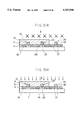
- FIGS. 11(a) to 11(g) are sectional views for illustrating a method for fabricating a CMOS driver circuit and a TFT of offset structure as a pixel switching element.
- This method utilizes a conventional CMOS driver circuit fabrication method as disclosed in, for example, Japanese Unexamined Patent Publication No. 286368/1992 and an offset TFT fabrication method as disclosed in Japanese Unexamined Patent Publication No. 275450/1993.
- FIG. 11(a) to 11(g) are sectional views for illustrating a method for fabricating a CMOS driver circuit and a TFT of offset structure as a pixel switching element.
- This method utilizes a conventional CMOS driver circuit fabrication method as disclosed in, for example, Japanese Unexamined Patent Publication No. 286368/1992 and an offset TFT fabrication method as disclosed in Japanese Unexamined Patent Publication No. 275450/1993.
- numeral 1 denotes an insulative substrate
- numeral 2 a polysilicon film for use as a channel semiconductor film
- numeral 3 a gate insulating film
- numeral 4 an n + -polysilicon containing phosphorus (hereinafter represented as P) at a high concentration and intended for a gate electrode
- numerals 16 and 26 n + -polysilicon layers implanted with P ion at a high concentration and intended for source/drain regions
- An n-channel TFT 10 as a pixel switching element herein shown is of offset structure
- n- and p-channel TFTs 20, 30 forming a CMOS driver circuit are not of offset structure but of typical planar structure.
- the TFTs of the aforementioned structure are fabricated by the following method.
- the semiconductor polysilicon film 2 to be used as a channel is formed on the insulative substrate 1, followed by forming the photoresist 5a (refer to FIG. 11(a)) and patterning the polysilicon film 2 to define islands for the TFTs.
- the gate insulating film 3 is then formed by a thermal oxidation process or a same process (refer to FIG. 11(b)).
- n + -polysilicon film 4 is formed (refer to FIG. 11(c)).
- a gate electrode pattern of photoresist 5b is formed only on the island intended for TFT 10 for use in a switching element of the pixel portion (that may be hereinafter referred to as the pixel switching TFT).
- the islands intended for the CMOS driver TFTs are entirely covered with the photoresist 5c and are not patterned.
- a gate electrode with eaves shown in FIG. 11(d) is formed by overetching of the n + -polysilicon, which is followed by dry-etching of the n + -polysilicon film in the thicknesswise direction thereof by using SF 6 gas or the like.
- the photoresist 5d is formed for the formation of gate electrodes of the CMOS driver circuit, and then the n + -polysilicon film is etched to form the gate electrodes 24, 34, as shown in FIG. 11(e). At this time, the pixel switching TFT 10 of offset structure is covered with the photoresist 5e.
- B-ion implantation is carried out to form source/drain regions 27, 37 of p + -polysilicon heavily doped with B. Thus, p-type TFT 30 is realized.
- n-type TFT 20 of the CMOS driver circuit is fabricated.
- the photoresists 5f, 5g are then exfoliated to realize the basic structure comprising the polysilicon TFT of offset structure to be used as the pixel switching element and the CMOS driver circuit, followed by the formation of source/drain electrodes.
- the polysilicon TFT of offset structure is used as the pixel switching element.
- a decrease in "OFF current” is of importance for the pixel switching element.
- crystal defects present at the grain boundary influence the polysilicon TFT in the "OFF state” to cause field emission current to flow in the drain region thereof, thereby increasing the "OFF current”. Accordingly, it is difficult to decrease the "OFF current” to the aforementioned value.
- offset regions are provided on opposite sides of the gate electrode as shown in FIGS. 11(d) to 11(g) so as to decrease the electric field of the drain region thereby to decrease the OFF current.
- the CMOS driver circuit region allows an "OFF current" of up to about 10 -9 A. Nevertheless, to realize a high speed operation, a high field effect mobility (i.e., high "ON current") is required. Since an offset region of a TFT serves as series resistance when the TFT is in the "ON state", the field effect mobility is lowered thereby. Therefore, the CMOS circuit employs polysilicon TFTs of the conventional planar type, not of the offset structure.
- the photolithographic process is required to be carried out at least three times and the dry etching process at least three times. This results in a lengthy production process.
- the CMOS driver circuit comprises the conventional planar TFTs, higher power source voltage causes a higher electric field to be applied to the drain region of TFT and, hence, a problem of extremely increased drain current will result. For this reason, the power source voltage to be applied to the CMOS transistors is restricted to at most 20 V. This also restricts the gate voltage and source voltage of the pixel switching TFT in driving the liquid crystal.
- the present invention has been attained to overcome the foregoing problems. It is, therefore, an object of the present invention to provide an active-matrix liquid crystal display integrally formed with a driver circuit which includes TFTs fabricated on one of a pair of substrates in a shortened process and a CMOS driver circuit adaptable for a high power voltage.
- Another object of the present invention is to provide a method for fabricating such an active-matrix liquid crystal display.
- an active-matrix liquid crystal display integrally formed with a driver circuit comprising:
- the pair of substrates comprises:
- a TFT substrate including at least an insulative substrate, source interconnection line and gate interconnection line which are formed in a matrix pattern on the insulative substrate, a thin film transistor provided to a pixel portion for use as a switching element for applying a voltage to a portion of the liquid crystal material which lies at a location where the source interconnection line and the gate interconnection line intersect each other, a pixel electrode connected to a drain electrode of the thin film transistor for supplying a voltage to the liquid crystal material, and a CMOS driver circuit having a CMOS which comprises thin film transistors for supplying an electric signal to the thin film transistor of the pixel portion through the source interconnection line and the gate interconnection line; and
- a counterpart substrate including an insulating substrate and a counter electrode formed thereon
- the thin film transistor provided to the pixel portion being of a first conductivity type and of an offset or LDD structure
- At least a first conductivity type thin film transistor of the thin film transistors of the CMOS driver circuit being of an offset or LDD structure.
- the first conductivity type herein is either n-type or p-type, and the second conductivity type is opposite to the first conductivity type. For example, if the first conductivity type is n-type, then the second conductivity type is p-type, and vice versa.
- the first conductivity type thin film transistor herein is a first conductivity type channel transistor having source/drain regions of the first conductivity type
- the second conductivity type thin film transistor is has a conductivity type which the reverse of the first conductivity type thin film transistor.
- a method for fabricating an active-matrix liquid crystal display integrally formed with a driver circuit wherein a liquid crystal material is sandwiched between a TFT substrate and a counterpart substrate having a counter electrode on an insulating substrate, the TFT substrate comprising an insulating substrate, thin film transistors arranged in a matrix pattern on the insulating substrate and each provided to an individual pixel portion for use as a switching element, and a CMOS driver circuit having a CMOS for driving the thin film transistor of each pixel portion, the method comprising formation of the thin film transistor of each pixel portion and the CMOS including a first conductivity type thin film transistor and a second conductivity type thin film transistor, the formation comprising at least the steps of:
- the method of the present invention may include the steps of:
- This method allows the thin film transistor of each pixel portion and the first conductivity type thin film transistor of the CMOS driver circuit to have an LDD structure instead of the offset structure.
- the ON current can be increased while restricting the OFF current compared to the ON current in the case of the offset structure.
- a method according to the present invention comprises formation of a thin film transistor of each pixel portion and first conductivity type thin film transistor and second conductivity type thin film transistor of a CMOS driver circuit, the formation comprising at least the steps of:
- This method may additionally include, between the steps (j) and (k), the step (m) of ion-implanting the first conductivity type impurity into the regions provided for the first conductivity type thin film transistor of the CMOS driver circuit and for the first conductivity type thin film transistor of each pixel portion with use of the gate electrodes as a mask to a concentration lower than the concentration of the first conductivity type impurity resulting from the preceding ion implantation.
- the channel semiconductor film in at least one of the regions provided for the first conductivity type thin film transistor and second conductivity type thin film transistor of the CMOS driver circuit is lightly doped with an impurity element of the conductivity type opposite to the conductivity type of the source/drain regions of the corresponding transistor. This advantageously permits the threshold voltage of the transistor to be controlled.
- the channel semiconductor film in the regions provided for the thin film transistor of each pixel portion and the first conductivity type thin film transistor of the CMOS driver circuit be lightly doped with the second conductivity type impurity. This allows the threshold voltage of these transistors to be controlled.
- the ion implantion of the second conductivity type impurity to the region provided for the second conductivity type thin film transistor is preferably achieved by an oblique implantation process which implants ions of the second conductivity type impurity at an angle of incidence of 20° or larger. This allows the transistor to have an decreased "OFF current".
- an additional step is preferably performed of ion-implanting the first conductivity type impurity to the gate electrode thin film in the region provided for the second conductivity type thin film transistor of the CMOS driver circuit after the formation of the gate electrode thin film to a concentration higher than the concentration of the second conductivity type impurity to be ion-implanted thereto later.
- the TFT of each pixel and the TFT of the same conductivity type as the TFT of each pixel are of offset or LDD structure. This arrangement permits the TFT of each pixel to have an "OFF current" lowered to not higher than about 10 -11 A while enabling the CMOS driver circuit to use a high power source voltage, thereby realizing a high speed operation.
- the TFT of each pixel and the TFT of the same conductivity type as the TFT of each pixel are fabricated in the same process. This makes it possible to reduce the number of times the photolithographic steps and the ion implantation steps are peformed by one each, compared to the conventional fabrication method. Further, certain examples of the method are able to reduce the number the times of etching steps are performed by one, compared to the conventional fabrication method.
- FIGS. 1(a) to 1(f) illustrate a fabrication process for TFT section of an AMLCD according to Example 1 of the present invention
- FIG. 2 illustrates one step of a fabrication process for TFT section of an AMLCD according to Example 2 of the present invention
- FIGS. 3(a) to 3(c) illustrate a fabrication process for TFT section of an AMLCD according to Example 3 of the present invention
- FIGS. 4(a) to 4(h) illustrate a fabrication process for TFT section of an AMLCD according to Example 4 of the present invention
- FIGS. 5(a) and 5(b) illustrate a fabrication process for TFT section of an AMLCD according to Example 5 of the present invention
- FIG. 6 is a graphic representation showing the relationship between the field effect mobility ( ⁇ ) and the offset length before and after a hydrogenation treatment
- FIGS. 7(a) to 7(e) illustrate a fabrication process for TFT section of an AMLCD according to Example 9 of the present invention
- FIGS. 8(a) and 8(b) illustrate a fabrication process for TFT section of an AMLCD according to Example 11 of the present invention
- FIG. 9 illustrates a fabrication process for TFT section of an AMLCD according to Example 13 of the present invention.
- FIG. 10 illustrates a fabrication process for TFT section of an AMLCD according to Example 14 of the present invention.
- FIGS. 11(a) to 11(g) illustrate a conventional fabrication process for TFT section of an AMLCD.
- an AMLCD typically includes a pair of opposing substrates with a predetermined clearance therebetween which are bonded together at the peripheral edges thereof, a liquid crystal material introduced into the clearance, polarizers disposed on both sides of the pair of substrates, a back light and the like.
- One of the substrates is a TFT substrate including an insulating substrate made of a material such as glass, plastic or the like on which are provided at least TFTs of pixel portions (hereinafter referred to as "pixel switching TFTs") and pixel electrodes arranged in a matrix pattern, signal buses, such as source interconnection lines and gate interconnection lines, which are extending longitudinally and transversely in a matrix manner to interconnect the pixel portions, a CMOS driver circuit comprising CMOS driver TFTs, i.e., an n-type TFT and a p-type TFT for driving each pixel switching TFT, and an alignment film.
- the other substrate is a counter electrode substrate including an insulating substrate similar to the abovementioned, on which are provided at least a counter electrode and optionally an alignment film, a black mask, a color filter and the like as required.
- the present invention provides an AMLCD comprising TFTs of improved structure respectively for each pixel and the CMOS driver circuit, and an improved fabrication method therefor.
- the AMLCD is characterized in that both the pixel switching TFT and the TFT of the CMOS driver circuit of the same conductivity type as the pixel switching TFT have an offset or LDD structure.
- the fabrication method of the present invention is characterized in that those TFTs are fabricated in the same process thereby reducing the number of photographic steps and that of etching steps.
- the present invention is similar to the conventional art in the features other than pointed out above and, hence, only the TFT structure of the TFT substrate and the fabrication method therefor will be described by way of specific examples thereof.
- FIGS. 1(a) to 1(f) illustrate one example of a fabrication process for a TFT section of an AMLCD according to the present invention.
- the TFT section includes an insulating substrate 1, a polysilicon film 2 for use as a channel semiconductor film, a gate insulating film 3, an n + -polysilicon 4 heavily doped with P and intended for gate electrodes, a photoresist 5 including 5a, 5b and 5c, source/drain regions 16, 26 and 36 implanted with P ion to a high concentration which are formed of, for example, n + -polysilicon, and source/drain regions 37 implanted with B ion to a high concentration which are formed of, for example, p + -polysilicon.
- a switching element n-type TFT of the pixel portion and the n-type TFT of the CMOS driver circuit are of offset structure, while the p-type TFT of the CMOS driver circuit is not of offset structure but of conventional planar structure.
- the semiconductor the devices of the abovementioned structures are fabricated according to the following method.
- the polysilicon film 2 for use as a channel semiconductor film is formed on the insulative substrate 1 by, for example, a low pressure CVD process, plasma CVD process or atmospheric pressure CVD, followed by forming the photoresist 5a (refer to FIG. 1(a)). Dry etching is then performed to define polysilicon islands.
- the polysilicon film may be formed by forming an amorphous silicon film using a plasma CVD process, low pressure CVD process or atmospheric pressure CVD process and thereafter carrying out a solid phase crystallization at 550° C. or above, or by forming an amorphous or polysilicon film followed by carrying out a laser annealing process.
- the gate insulating film 3 is formed by a thermal oxidation process, low pressure CVD process, atmospheric CVD process, ECR plasma CVD process, plasma VD process or a like process, or by combining two or more of these processes (refer to FIG. 1(b)).
- the gate electrode thin film 4, such as of n + -polysilicon, intended for the gate electrodes is formed by, for example, a low pressure CVD process (refer to FIG. 1(c)).
- the photoresist 5b is formed and then the n + -polysilicon thin film 4 is etched using, for example, SF 6 gas to form patterns of the gate electrodes 14, 24 and 34.
- the completion of the dry etching is judged by monitoring fluorine radicals having a spectrum of 704 nm, followed by overetching for a predetermined time period to side-etch the n + -polysilicon thin film 4. This enables the width of each of the resulting gate electrodes 14, 24 and 34 to become narrower than the width of the photoresist pattern.
- the gate electrodes 14, 24 and 34 in combination with the photoresist thereon form projecting structures.
- the projecting structures may be formed by overetching the metal in accordance with a wet etching process.
- P ions are implanted into the polysilicon islands to a high concentration to form the source/drain regions 16, 26 and 36 of n + -polysilicon film heavily doped with P.
- the regions provided for each pixel switching TFT 10 and the n-type TFT 20 of the CMOS driver circuit are covered with the photoresist 5c, and then the region provided for the p-type TFT 30 of the CMOS driver circuit is implanted with B ion thereby forming source/drain region 37 of p + -polysilicon layer heavily doped with B.
- the amount of B to be ion-implanted is desired to be set so that the B concentration resulting from the ion implantation will exceed the concentration of P implanted at the step of FIG. 1(d) in terms of effective concentration determined in view of the activation yield of each impurity at the time of completion of activation thereof.
- the activation yield at the time of completion of activation herein is the ratio of the amount of an impurity having released the carrier to the total amount of the impurity contained in the film. It is desirable that the semiconductor assume a desired conductivity type after the activation of the impurity.
- the photoresist 5c is removed to complete the n-type offset TFT 10 for use as the switching element of each pixel and the n-type offset TFT 20 and p-type TFT 30 of the CMOS driver circuit.
- this method it is possible to fabricate these TFTs 10, 20 and 30 by carrying out dry etching step twice and photolithographic step three times.
- the subject method employs the ion implantation to dope the silicon thin film with impurities, a diffusion process or a like technique may be employed instead of the ion implantation.
- a diffusion process or a like technique may be employed instead of the ion implantation.
- P is used as the n-type impurity in this Example, arsenic (hereinafter referred to as "As") may be used instead.
- the TFT 10 for use as the switching element of each pixel is of offset structure polysilicon. It is important that the pixel switching TFT 10 have a decreased "OFF current". Generally, the "OFF current" is desirably not higher than about 10 -11 A. However, it is difficult to decrease the "OFF current” to such a value or lower since the TFT of polysilicon in the "OFF state" is affected by crystal defects present at grain boundary, so that field emission current flows in the drain region. For this reason, offset regions 19 and 29 are provided on both sides of the gate electrode as in the TFTs 10 and 20 shown in FIG. 1(f) to decrease the electric fields of the drain regions 16 and 26 thereby decreasing the "OFF current".
- the n-type TFT 20 of the CMOS driver circuit region is of the offset structure, this offset region in the TFT 20 acts as a series resistor and, hence, the "ON current" may be decreased.
- This problem is solved by optimizing the offset length and the material characteristics of Si.
- the offset length can be precisely controlled by using the side etching technique against the n + -polysilicon film forming the gate electrodes 14 and 24. In a TFT actually fabricated the offset length is about 0.2 ⁇ m to about 2.0 ⁇ m.
- To increase the "ON current” it is required to reduce the series resistance of the offset regions, or specifically, to improve the material characteristics of polysilicon. To this end, polysilicon is subjected to a hydrogenation treatment.
- the hydrogenation treatment causes the drain current of the TFT to increase substantially.
- the hydrogenation treatment utilizes hydrogen plasma generated by the use of ECR (Electron Cyclotron Resonance) plasma so as to be achieved at a high efficiency.
- the hydrogenation treatment may be based on a typical parallel flat plate high frequency plasma CVD, hydrogen ion implantation, or a method of supplying hydrogen by forming an SiN x using a plasma CVD and annealing the SiN x film.
- the polysilicon is heat-treated at a high temperature, for example, at least 700° C.
- the heat treatment for improving the material characteristics of the polysilicon may be performed at the same time therewith.
- the temperature for heat treatment is desirably at least about 900° C.
- the source/drain regions 37 comprising p + -polysilicon formed by B ion implantation are formed to construct the p-type TFT 30 of the CMOS driver circuit.
- the n + -polysilicon film 34 serving as the gate electrode of the p-type TFT 30 of the CMOS driver circuit is also implanted with B. Accordingly, P contained in the gate electrode is compensated by B, so that the concentration of effective carrier in the film decreases and the resistance of the gate electrode increases. Further, if the B concentration exceeds the P concentration, the conductivity type of the gate electrode turns into p-type. This results in a problem of a substantially increased threshold voltage Vth of the TFT. For this reason, the process needs to be controlled so that the P concentration of the gate electrode will at least be higher than the concentration of B implanted into the gate electrode film in terms of effective concentration of each impurity determined in view of the activation yield thereof after the completion of activation.
- Example 1 the source/drain regions 37 comprising p + -polysilicon formed by B ion implantation are formed to construct the p-type TFT 30 of the CMOS driver circuit.
- the n + -polysilicon film 34 serving as the gate electrode of the p-type TFT 30 of the CMOS driver circuit is also implanted with B. Accordingly, P contained in the gate electrode is compensated by B, so that the concentration of effective carrier in the film decreases and the resistance of the gate electrode increases. Further, if the B concentration exceeds the P concentration, the conductivity type of the gate electrode turns into p-type. This results in a problem of a substantially increased threshold voltage Vth of the TFT.
- This Example does not need to set the P concentration of the gate electrode in excess in view of the amount of P to be compensated by B.
- each pixel switching n-type TFT 10 and the n-type TFT 20 of the CMOS driver circuit are of LDD structure, while the p-type TFT 30 of the CMOS driver circuit is not of the LDD structure but of the typical planar structure.
- the fabrication method for the TFT section of the AMLCD according to this example is as follows:
- insulating substrate 1 On insulating substrate 1 are sequentially formed islands of channel semiconductor layer 2, gate insulatig film 3 and gate electrodes 4, followed by implantation of P ion using photoresist 5b of projecting structure as a mask thereby forming source/drain regions 16, 26 and 36 of n + -polysilicon heavily doped with P, as shown in FIGS. 1(a) to 1(d).
- P ions are implanted to a low concentration, for example, about 1 ⁇ 10 16 cm -3 to about 1 ⁇ 10 19 cm -3 to form LDD regions 18, 28 and 38, as shown in FIG. 3(a).
- the dose of P ions is about 1 ⁇ 10 11 cm -2 to about 1 ⁇ 10 14 cm -2 .
- the region for the p-type TFT 30 of the CMOS driver circuit is implanted with B ion to form source/drain regions 37 of p + -polysilicon layer heavily doped with B in the p-type TFT region of the CMOS driver circuit.
- the ion implantation technique is employed to dope the Si thin film with an impurity
- the diffusion technique or a like technique may be employed instead.
- n-type impurity instead of P.
- the step shown in FIG. 3(a) may be interchanged with the other step shown in FIG. 3(b).
- the LDD regions 18 and 28 are formed on opposite sides of respective gate electrodes 14 and 24 of the pixel switching TFT 10 and the n-type TFT 20 of the CMOS driver circuit.
- the resistance of the LDD regions when TFTs are in the "ON state” is lower than that of the offset regions and, hence, the "ON current” is further improved. This results in the CMOS circuit offering an improved driving frequency.
- FIGS. 4(a) to 4(h) A fourth example of the present invention will be described with reference to FIGS. 4(a) to 4(h).
- numerals 12b and 22b denote a semiconductor film made of a material such as p - -polysilicon for use as a channel lightly doped with B, and other same numerals denote like parts of Examples 1 and 3.
- the pixel switching n-type TFT 10 and the n-type TFT 20 of the CMOS driver circuit are of the LDD structure, while the p-type TFT 30 of the CMOS driver circuit is not of the LDD structure but of the typical planar structure.
- the TFT section of the structure shown is fabricated according to the following method.
- a channel semiconductor film 2 made of a material such as polysilicon film is formed on an insulating substrate 1 by, for example, low pressure CVD process, followed by forming a photoresist 5a. Dry etching is then performed to define polysilicon islands.
- the polysilicon film may be formed by forming an amorphous silicon film using plasma CVD process, low pressure CVD process or atmospheric pressure CVD process and thereafter carrying out solid phase crystallization at least 550° C., or by forming an amorphous silicon or polysilicon film followed by carrying out a laser annealing process.
- a gate insulating film 3 is formed by a thermal oxidation process, low pressure CVD process, atmospheric CVD process or a like process (refer to FIGS. 4(a) and 4(b)).
- the procedure up to this step is the same as in Example 1.
- the island region provided for the formation of the p-type TFT 30 of the CMOS driver circuit is covered with a photoresist 5b and then a p-type impurity such as B is ion-implanted to the regions provided for the formation of the pixel switching n-type TFT 10 and n-type TFT 20 of the CMOS driver circuit to adjust the threshold voltage (Vth) thereof.
- the dose of the p-type impurity has to be relatively small for light doping (refer to FIG. 4(c)). Ion implantation of B may be performed only to the region provided for the on-type TFT of the CMOS driver circuit.
- Another light doping step may be added so as to adjust the threshold voltage of the p-type TFT 30 of the CMOS driver circuit.
- the regions provided for the pixel switching n-type TFT 10 and n-type TFT 20 of the CMOS driver circuit are covered with photoresist to prevent a threshold adjust impurity atoms from being implanted to these TFTs.
- Ion implantation of B for adjusting the threshold voltage Vth of the pixel switching n-type TFT 10 and n-type TFT 20 of the CMOS driver circuit may be performed prior to the formation of the gate insulating film 3 and after the formation of photoresist covering the p-type TFT region of the CMOS driver circuit.
- the gate insulating film 3 is formed using, solely or in combination, thermal oxidation process, low pressure CVD process, atmospheric pressure CVD process, ECR plasma CVD process or plasma CVD process after the removal of the photoresist.
- a gate electrode thin film 4 made of a material such as n + -polysilicon is formed by, for example, low pressure CVD process (refer to FIG. 4(d)).
- a photoresist 5c is formed and then the n + -polysilicon film is etched using, for example, SF 6 gas to form patterns of gate electrodes 14, 24 and 34.
- the completion of the dry etching against the n + -polysilicon film is judged by monitoring fluorine radicals having a spectrum of 704 nm as in Example 1.
- over-etching is carried out for a predetermined time period to cause the n + -polysilicon film to be side-etched, thereby forming a projection structure comprising each of the gate electrodes 14, 24 and 34 and the overlying photoresist.
- a metal may be used to form the gate electrodes, which is over-etched by, for example, wet etching to form the projection structure.
- ion implantation of P is carried out to form source/drain regions 16, 26 and 36 comprising an n + -polysilicon film.
- an n-type impurity such as P is ion-implanted to a low concentration (light doping) to form LDD regions 18, 28 and 38.
- the dose of ion in this ion implantation is about 1 ⁇ 10 11 cm -2 to about 1 ⁇ 10 14 cm -2 and is desirably set to have a concentration larger than the concentration of B lightly-implanted to the regions for the pixel switching TFT 10 and n-type TFT 20 of the CMOS driver circuit in terms of effective concentration determined in view of the activation yield of each impurity at the time of the completion of activation.
- the regions for the pixel switching TFT 10 and n-type TFT 20 of the CMOS driver circuit are covered with a photoresist 5d, and then ion implantation of B is carried out to form source/drain regions 37 comprising a p + -polysilicon layer heavily doped with B in the region for the p-type TFT 30 of the CMOS driver circuit.
- the amount of B to be ion-implanted is desirably set to exceed that of P previously implanted at the step of FIG. 4(e) in terms of effective concentration determined in view of the activation yield of each impurity at the completion of activation.
- the photoresist 5d is removed to complete the pixel switching n-type TFT 10 of LDD structure, n-type TFT 20 of the CMOS driver of LDD structure and p-type TFT 30 of the CMOS driver circuit.
- ion implantation is used to dope Si thin film with an impurity in the above method
- a diffusion technique may be used instead.
- As may be used as the n-type impurity instead of P.
- Example 2 The basic operation of the TFT section in this Example is the same as described in Example 1.
- the channel region of each of the pixel switching TFT 10 and n-type TFT 20 of the CMOS driver circuit is lightly doped with B. This allows the threshold voltage Vth of both TFTs 10 and 20 to be positively raised. For this reason, the drain current at the time when the gate voltage is 0 V decreases and, hence, the transfer characteristic of an inverter is improved particularly in the CMOS driver circuit.
- the input voltage (Vin) is 0 V
- a decrease in the output voltage (Vout) due to leak current of the n-type TFT can be avoided.
- the LDD regions 18 and 28 are provided on the opposite sides of the respective gate electrodes of the TFTs 10 and 20. This allows the electric resistance of the TFTs in "ON state” to decrease rather than the TFTs of offset structure, thereby improving the "ON current” thereof. This results in an improvement in the drive frequency of the CMOS driver circuit.
- ion implantation of B is carried out to form the p-type TFT of the CMOS driver circuit.
- the so-called oblique implantation may be carried out for obliquely implanting B ion to a low concentration as shown in FIG. 5(a), followed by a usual ion implantation for a high concentration implant as shown in FIG. 5(b).
- a process shown in FIG. 5(a) may be changed to a process shown in FIG. 5(b) with each other.
- the angle of incidence of ion is slanted at least at 20° with respect to a line perpendicular to the surface of the substrate.
- Such an ion implantation technique enables the formation of an overlap LDD structure under the corresponding gate electrode. Hence, it is possible to improve the withstand voltage of the p-type TFT 30 of the CMOS driver circuit against the drain voltage when the source/drain electrode 37 is applied with a voltage. Accordingly, the power source voltage for the CMOS circuit can further be improved, and this leads to an advantage of, for example, an improved output voltage of the inverter circuit.
- the pixel switching TFT comprises an n-type TFT of offset structure, but may comprise a p-type TFT instead.
- the fabrication method for the TFT section is basically the same as shown in FIGS. 1(a) to 5(b), associated with Examples 1 to 5.
- P has to be replaced with B and vice versa, for example, the P ion implantation is replaced with B ion implantation and vice versa.
- the description on the gate electrodes is not changed.
- the light doping of B for adjusting threshold voltage Vth at the step of FIG. 4(c) may be carried out with respect only to the region for the CMOS driver n-type TFT 20.
- B need not necessarily be replaced with P.
- the n-type impurity may comprise As instead of P.
- the gate electrodes may comprise a p + -polysilicon thin film instead of the n + -polysilicon thin film.
- other structural features are the same as in Examples 1 to 6.
- each TFT comprises a single gate TFT having one gate electrode, but it may comprise two or more TFTs connected in series so as to provide two or more gate electrodes between the source/drain regions. In this case too, other structural features are the same as in Examples 1 to 7.
- FIGS. 7(a) to 7(e) are sectional views for illustrating a process for fabricating a TFT array according to Example 9.
- a channel polysilicon film 2 for use as a channel layer is formed on an insulating substrate 1 such as made of quartz or glass using a low pressure CVD process.
- This channel polysilicon film 2 is patterned and then subjected to a thermal oxidation process to form a gate insulating film 3 of about 120 nm thickness.
- a gate electrode thin film 4 of, for example, Si doped with P is formed over the entire substrate surface.
- the polysilicon film 2 may be formed by forming an Si film using a low pressure CVD and then crystallizing the same by solid phase epitaxy, laser annealing or a like process, or forming an Si film by a plasma CVD process and then crystallizing the same by solid phase epitaxy, laser annealing or a like process.
- the gate insulating film 3 may be formed by forming an SiO 2 film or the like by a sputtering process, a low pressure CVD process or an atmospheric pressure CVD process. These processes each may be used in combination with a thermal oxidation process.
- the thin film to be used for gate electrode may be formed of an Si film doped with B or As, a metal thin film of aluminum, aluminum alloy or chromium, or a suicide thin film of molybdenum silicide, tungsten silicide or titanium silicide, as well as of the foregoing Si film doped with P.
- a photoresist 5a is formed as covering the entire region for the p-type TFT 30 of the CMOS driver circuit and the gate electrode formation regions of the n-type TFT 20 of the CMOS driver circuit and pixel switching n-type TFT 10.
- the gate electrode thin film 4, such as of Si, to be used as gate electrode is dry-etched using a gas mainly containing SF 6 , CF 4 , NF 3 , Cl 2 or the like which is adapted for isotropic etching, thereby patterning the gate electrode thin film 4 as having a width smaller than the photoresist 5a by about 0.3 ⁇ m to about 2.0 ⁇ m.
- an n-type impurity such as P or As is ion-implanted to the substrate surface with the photoresist 5a retained as it is, thereby forming n-type source/drain regions 16 and 26 respectively having offset regions 19 and 29 in the regions for the pixel switching n-type TFT 10 and n-type TFT 20 of the CMOS driver circuit.
- the length of the offset regions 19 and 29 is in the range of 0.3 ⁇ m to 2.0 ⁇ m, depending upon how much the the gate electrodes 14, 24 and 34 have been side-etched in the preceeding step.
- the photoresist 5a on the gate electrodes 14 and 24 also serves to prevent the ion-implanted impurity from penetrating into the gate insulating film 3 and channel regions 12, 22 underlying the gate electrodes 14, 24 of the n-type TFTs 10, 20.
- the n-type TFT 20 of the CMOS driver circuit and the pixel switching n-type TFT 10 are covered with a photoresist 5b, and then the gate electrode 34 of the p-type TFT 30 of the CMOS driver circuit is formed by patterning using the photoresist 5b, followed by ion implantation of a p-type impurity such as B with the photoresist 5b retained. This allows p-type source/drain regions 37 to be formed in p-type TFT region of the CMOS driver circuit.
- the photoresist 5b on the gate electrode 34 also serves to prevent the ion-implanted impurity from penetrating into the gate electrode 34, underlying gate insulating film 3 and channel region of the p-type TFT 30.
- the p-type TFT 30 is not of offset structure, but it may be of offset structure formed by isotropic etching.
- the thus described TFT array fabrication method enables a reduction in the number of steps required to form the pixel switching n-type TFT of offset structure and the TFTs of the CMOS driver circuit on the same substrate and hence realizes a reduction in the manufacturing cost and a high throughput.
- offset structure of the n-type TFT of the CMOS driver circuit enables the CMOS driver TFTs to use a high source voltage.
- the region for the p-type TFT 30 is masked in ion-implanting the impurity to the n-type TFTs. This enables the amount of the impurity such as B to be implanted to the p-type TFT to be reduced thereby offering an advantage of realizing a high throughput.
- Example 9 employs an n-type TFT as the pixel switching TFT.
- the p-type TFT of the CMOS driver circuit and the pixel switching p-type TFT can be simultaneously formed as having offset structure. This also makes it possible to reduce the number of fabrication steps and to provide TFTs of the CMOS driver circuit capable of using a high power source voltage.
- the TFT array of this Example can be fabricated according to the fabrication method described in Example 9 except that the p-type impurity is ion-implanted in the first implantation process while the n-type impurity is ion-implanted in the second implantation process.
- Example 9 employs the offset structure for the pixel switching n-type TFT 10 and n-type TFT 20 of the the CMOS driver circuit
- the present Example employs the LDD structure therefor.
- the fabrication method according to this Example is as follows. This fabrication method follows the method of Example 9 up to the step of ion implantation of the n-type impurity as shown in FIG. 7(d) to form n-type TFTs 10 and 20 of offset structure.
- an n-type impurity such as P or As is ion-implanted to a low concentration using gate electrodes 14 and 24 as a mask.
- the acceleration voltage is required to be set to prevent the n-type impurity from passing through the gate electrodes 14 and 24 and penetrating into the gate insulating film or the channel regions 12 and 22.
- an Si thin film 4 to be used as the gate electrode is retained in the region provided for the formation of the p-type TFT 30 of the CMOS driver circuit and serves as a mask thereby preventing the n-type impurity from penetrating into the Si portion to serve as a channel region.
- the n-type TFT 20 of the CMOS driver circuit and the pixel switching n-type TFT 10 are covered with a photoresist 5b, followed by forming the gate electrode 34 of the p-type TFT 30 of the CMOS driver circuit by patterning using the photoresist 5b. Ion implantation of a p-type impurity such as B is then performed with the photoresist 5b retained as it is. This results in the formation of p-type source/drain regions 37 in the p-type TFT 30 of the CMOS driver circuit.
- the thus described TFT array fabrication method enables a reduction in the number of steps required to form the pixel switching n-type TFT of LDD structure and TFTs of the CMOS driver circuit on the same substrate and hence realizes a reduction in manufacturing cost and a high throughput.
- the LDD structure of the n-type TFT of the CMOS driver circuit enables the TFTs of the CMOS driver circuit to use a high source voltage.
- the LDD structure employed in this Example allows the resistance of the TFTs in "ON state" to decrease rather than the TFTs of offset structure, thereby improving the "ON current" thereof. This results in an improvement in the drive frequency of the CMOS driver circuit.
- the region for the p-type TFT 30 is covered with the Si thin film 34 in forming the n-type TFTs of LDD structure, thereby preventing the impurity such as P from penetrating into the p-type TFT region.
- This enables the amount of the impurity such as B to be implanted to the p-type TFT 30 to be reduced thereby offering an advantage of realizing a high throughput.
- Example 11 employs an n-type TFT as the pixel switching TFT.
- the p-type TFT of the CMOS driver circuit and the pixel switching TFT can be simultaneously formed as having LDD structure. This also makes it possible to reduce she number of fabrication steps required and to provide TFTs of the CMOS driver circuit capable of using a high power source voltage and a high drive frequency.
- the TFT array of this Example can be fabricated according to the fabrication method described in Example 11 except that in the three ion implantation steps the p-type impurity is ion-implanted instead of the n-type impurity while the n-type impurity is ion-implanted instead of the p-type impurity.
- Example 11 provides the same effects as does Example 11.
- the p-type impurity such as B is vertically implanted to form the source/drain regions 37 of the p-type TFT of the CMOS driver circuit.
- the oblique implantation may be carried out for obliquely implanting the p-type impurity as shown in FIG. 9.
- Such an ion implantation technique enables the formation of an overlap LDD structure under the corresponding gate electrode.
- the n-type impurity such as P or As is vertically implanted to form the source/drain regions of the n-type TFT of the CMOS driver circuit.
- the oblique implantation may be employed for obliquely implanting the p-type impurity as shown in FIG. 10.
- Such an ion implantation technique enables the formation of an overlap LDD structure under the corresponding gate electrode.
- Examples 9 to 14 do not employ channel doping
- the AMLCD of the present invention employs an offset structure or LDD structure for one of the n- and p-type TFTs of the CMOS driver circuit. This allows the CMOS driver circuit to use a power source of high power source voltage, the output voltage of the driver circuit to be enhanced, and the operational range of the pixel switching TFT to be broadened. Thus, the AMLCD of the present invention exhibits high performance.
- the AMLCD fabrication method of the present invention applies the offset structure or LDD structure to one of the TFTs of the CMOS driver circuit which is of the same conductivity type as the pixel switching TFT and fabricates these two TFTs in common fabrication process.
- This makes it possible to reduce the number of times of photolithographic steps by one time and the number of times of ion implantation steps by one time, and further, in some aspects of the invention the number of times of etching steps can be reduced by one time.
- the method of the present invention enables the number of times of required fabrication steps to be reduced.
- the fabrication method of the present invention makes it possible to lower the production cost and improve the throughput and, hence, provides an inexpensive AMLCD.
Landscapes
- Engineering & Computer Science (AREA)
- Power Engineering (AREA)
- Microelectronics & Electronic Packaging (AREA)
- Physics & Mathematics (AREA)
- Condensed Matter Physics & Semiconductors (AREA)
- General Physics & Mathematics (AREA)
- Computer Hardware Design (AREA)
- Ceramic Engineering (AREA)
- Manufacturing & Machinery (AREA)
- Thin Film Transistor (AREA)
Abstract
An active-matrix liquid crystal display integrally formed with a driver circuit including: a pair of substrates disposed in opposing relation to each other; and a liquid crystal material sandwiched between the pair of substrates, wherein the pair of substrates includes: a TFT substrate including at least an insulative substrate, source interconnection line and gate interconnection line which are formed in a matrix pattern on the insulative substrate, a thin film transistor provided to each pixel portion for use as a switching element for applying a voltage to a portion of the liquid crystal material which lies at a location where the source interconnection line and the gate interconnection line intersect each other, a pixel electrode connected to a drain electrode of the thin film transistor for supplying a voltage to the liquid crystal material, and a CMOS driver circuit having a CMOS which comprises thin film transistors for supplying an electric signal to the thin film transistor of the pixel portion through the source interconnection line and the gate interconnection line; and a counterpart substrate including an insulative substrate and a counter electrode formed thereon, the thin film transistor provided to the pixel portion being of a first conductivity type and of an offset or LDD structure, at least a first conductivity type thin film transistor of the thin film transistors of the CMOS driver circuit being of an offset or LDD structure.
Description
This application is a continuation, of application Ser. No. 08/359,560, filed Dec. 20, 1994 now abandoned.
The present invention relates to an active-matrix liquid crystal display (hereinafter may be referred to as "AMLCD") of the type integrally formed with driver 5 circuitry which employs thin film transistors (hereinafter may be referred to as "TFTs") as pixel switching elements and CMOS driver circuit transistors, and to a fabrication method therefor.
FIGS. 11(a) to 11(g) are sectional views for illustrating a method for fabricating a CMOS driver circuit and a TFT of offset structure as a pixel switching element. This method utilizes a conventional CMOS driver circuit fabrication method as disclosed in, for example, Japanese Unexamined Patent Publication No. 286368/1992 and an offset TFT fabrication method as disclosed in Japanese Unexamined Patent Publication No. 275450/1993. In FIG. 11(a) to 11(g), numeral 1 denotes an insulative substrate, numeral 2 a polysilicon film for use as a channel semiconductor film, numeral 3 a gate insulating film, numeral 4 an n+ -polysilicon containing phosphorus (hereinafter represented as P) at a high concentration and intended for a gate electrode, numerals 5a, 5b, 5c, 5d, 5e, 5f and 5g photoresists, numerals 16 and 26 n+ -polysilicon layers implanted with P ion at a high concentration and intended for source/drain regions, and numerals 27 and 37 p+ -polysilicon layers implanted with boron (hereinafter represented as B) ion at a high concentration. An n-channel TFT 10 as a pixel switching element herein shown is of offset structure, while n- and p- channel TFTs 20, 30 forming a CMOS driver circuit are not of offset structure but of typical planar structure.
The TFTs of the aforementioned structure are fabricated by the following method. The semiconductor polysilicon film 2 to be used as a channel is formed on the insulative substrate 1, followed by forming the photoresist 5a (refer to FIG. 11(a)) and patterning the polysilicon film 2 to define islands for the TFTs. The gate insulating film 3 is then formed by a thermal oxidation process or a same process (refer to FIG. 11(b)).
In turn, the n+ -polysilicon film 4 is formed (refer to FIG. 11(c)).
In turn, as shown in FIG. 11(d), a gate electrode pattern of photoresist 5b is formed only on the island intended for TFT 10 for use in a switching element of the pixel portion (that may be hereinafter referred to as the pixel switching TFT). At this time, the islands intended for the CMOS driver TFTs are entirely covered with the photoresist 5c and are not patterned. To make the offset structure, a gate electrode with eaves shown in FIG. 11(d) is formed by overetching of the n+ -polysilicon, which is followed by dry-etching of the n+ -polysilicon film in the thicknesswise direction thereof by using SF6 gas or the like. Subsequently P is ion-implanted to the resulting substrate surface to form the n+ -polysilicon 16 heavily doped with P. In this case, the portion below the eaves of photoresist is not ion-implanted and, hence, the offset structure is realized.
After the photoresists 5b, 5c have been exfoliated, the photoresist 5d is formed for the formation of gate electrodes of the CMOS driver circuit, and then the n+ -polysilicon film is etched to form the gate electrodes 24, 34, as shown in FIG. 11(e). At this time, the pixel switching TFT 10 of offset structure is covered with the photoresist 5e. After the formation of the gate electrodes, B-ion implantation is carried out to form source/drain regions 27, 37 of p+ -polysilicon heavily doped with B. Thus, p-type TFT 30 is realized.
In turn, as shown in FIG. 11(f), after the pixel switching TFT 10 of offset structure and the p-type TFT 30 of the CMOS driver circuit are covered with photoresists 5f and 5g, respectively, P-ion implantation is carried out to a high concentration to form source/drain regions 26 of n+ -polysilicon. Thus, n-type TFT 20 of the CMOS driver circuit is fabricated.
The photoresists 5f, 5g are then exfoliated to realize the basic structure comprising the polysilicon TFT of offset structure to be used as the pixel switching element and the CMOS driver circuit, followed by the formation of source/drain electrodes.
Reference is then made to the operation of the thus formed structure. As described above, the polysilicon TFT of offset structure is used as the pixel switching element. A decrease in "OFF current" is of importance for the pixel switching element. Typically, it is desirable to decrease the "OFF current" to about 10-11 A or below. However, crystal defects present at the grain boundary influence the polysilicon TFT in the "OFF state" to cause field emission current to flow in the drain region thereof, thereby increasing the "OFF current". Accordingly, it is difficult to decrease the "OFF current" to the aforementioned value. For this reason, offset regions are provided on opposite sides of the gate electrode as shown in FIGS. 11(d) to 11(g) so as to decrease the electric field of the drain region thereby to decrease the OFF current.
On the other hand, the CMOS driver circuit region allows an "OFF current" of up to about 10-9 A. Nevertheless, to realize a high speed operation, a high field effect mobility (i.e., high "ON current") is required. Since an offset region of a TFT serves as series resistance when the TFT is in the "ON state", the field effect mobility is lowered thereby. Therefore, the CMOS circuit employs polysilicon TFTs of the conventional planar type, not of the offset structure.
In constructing the basic TFT structure shown in FIGS. 11(d) to 11(g) comprising the pixel switching TFT of offset structure and the CMOS driver circuit according to the conventional method, the photolithographic process is required to be carried out at least three times and the dry etching process at least three times. This results in a lengthy production process. Further, since the CMOS driver circuit comprises the conventional planar TFTs, higher power source voltage causes a higher electric field to be applied to the drain region of TFT and, hence, a problem of extremely increased drain current will result. For this reason, the power source voltage to be applied to the CMOS transistors is restricted to at most 20 V. This also restricts the gate voltage and source voltage of the pixel switching TFT in driving the liquid crystal.
The present invention has been attained to overcome the foregoing problems. It is, therefore, an object of the present invention to provide an active-matrix liquid crystal display integrally formed with a driver circuit which includes TFTs fabricated on one of a pair of substrates in a shortened process and a CMOS driver circuit adaptable for a high power voltage.
Another object of the present invention is to provide a method for fabricating such an active-matrix liquid crystal display.
According to one aspect of the present invention, there is provided an active-matrix liquid crystal display integrally formed with a driver circuit comprising:
a pair of substrates disposed in opposing relation to each other; and
a liquid crystal material sandwiched between the pair of substrates;
wherein the pair of substrates comprises:
a TFT substrate including at least an insulative substrate, source interconnection line and gate interconnection line which are formed in a matrix pattern on the insulative substrate, a thin film transistor provided to a pixel portion for use as a switching element for applying a voltage to a portion of the liquid crystal material which lies at a location where the source interconnection line and the gate interconnection line intersect each other, a pixel electrode connected to a drain electrode of the thin film transistor for supplying a voltage to the liquid crystal material, and a CMOS driver circuit having a CMOS which comprises thin film transistors for supplying an electric signal to the thin film transistor of the pixel portion through the source interconnection line and the gate interconnection line; and
a counterpart substrate including an insulating substrate and a counter electrode formed thereon,
the thin film transistor provided to the pixel portion being of a first conductivity type and of an offset or LDD structure,
at least a first conductivity type thin film transistor of the thin film transistors of the CMOS driver circuit being of an offset or LDD structure.
The first conductivity type herein is either n-type or p-type, and the second conductivity type is opposite to the first conductivity type. For example, if the first conductivity type is n-type, then the second conductivity type is p-type, and vice versa.
Further, the first conductivity type thin film transistor herein is a first conductivity type channel transistor having source/drain regions of the first conductivity type, and the second conductivity type thin film transistor is has a conductivity type which the reverse of the first conductivity type thin film transistor.
According to another aspect of the present invention, there is provided a method for fabricating an active-matrix liquid crystal display integrally formed with a driver circuit wherein a liquid crystal material is sandwiched between a TFT substrate and a counterpart substrate having a counter electrode on an insulating substrate, the TFT substrate comprising an insulating substrate, thin film transistors arranged in a matrix pattern on the insulating substrate and each provided to an individual pixel portion for use as a switching element, and a CMOS driver circuit having a CMOS for driving the thin film transistor of each pixel portion, the method comprising formation of the thin film transistor of each pixel portion and the CMOS including a first conductivity type thin film transistor and a second conductivity type thin film transistor, the formation comprising at least the steps of:
(a) sequentially forming a channel semiconductor film, a gate insulating film and a gate electrode thin film on the insulating substrate in regions thereof provided for the thin film transistor of each pixel portion and for the first conductivity type thin film transistor and second conductivity type thin film transistor of the CMOS driver circuit, followed by forming a photoresist on the gate electrode thin film for finely patterning the gate electrode thin film;
(b) etching an electrode thin film with use of the photoresist as a mask to form gate electrodes each narrower than the photoresist;
(c) ion-implanting a first conductivity type impurity to a high concentration into source/drain regions lying on both sides of each of the gate electrodes with use of the photoresist as a mask to form three kinds of first conductivity type thin film transistors of an offset structure and afterword removing the photoresist; and
(d) covering at least the thin film transistor of each pixel portion and the thin film transistor intended for the first conductivity type thin film transistor of the CMOS driver circuit with a photoresist and ion-implanting a second conductivity type impurity into the thin film transistor intended for the second conductivity type thin film transistor of the CMOS driver circuit to a concentration higher than the concentration of the first conductivity type impurity in terms of an effective concentration determined in view of the activation yield of each impurity at the time of completion of the activation thereof, to form the second conductivity type thin film transistor of the CMOS driver circuit.
Instead of the step (d), the method of the present invention may include the steps of:
(e) ion-implanting the first conductivity type impurity to the three kinds of thin film transistors to a low concentration thereby making all the three kinds of thin film transistors have a first conductivity type LDD structure; and
(f) covering at least the regions provided for the thin film transistor of each pixel portion and the thin film transistor intended for the first conductivity type thin film transistor of the CMOS circuit with a photoresist and ion-implanting the second conductivity type impurity into the thin film transistor intended for the second conductivity type thin film transistor of the CMOS driver circuit to a concentration higher than the concentration of the first conductivity type impurity in terms of an effective concentration determined in view of the activation yield of each impurity at the time of completion of the activation thereof, to form the second conductivity type thin film transistor of the CMOS driver circuit.
This method allows the thin film transistor of each pixel portion and the first conductivity type thin film transistor of the CMOS driver circuit to have an LDD structure instead of the offset structure. By virtue of the LDD structure the ON current can be increased while restricting the OFF current compared to the ON current in the case of the offset structure.
Alternatively, a method according to the present invention comprises formation of a thin film transistor of each pixel portion and first conductivity type thin film transistor and second conductivity type thin film transistor of a CMOS driver circuit, the formation comprising at least the steps of:
(g) sequentially forming a semiconductor film and a gate insulating film on an insulating substrate, followed by forming a gate electrode thin film over the entire substrate surface;
(h) masking with a photoresist a region provided for the second conductivity type thin film transistor of the CMOS driver circuit and regions provided for respective gate electrodes of the first conductivity type thin film transistor of the CMOS driver circuit and first conductivity type thin film transistor of each pixel portion, followed by patterning the gate electrode thin film by isotropic etching, thereby forming the gate electrodes, each of which is narrower than the photoresist masking the same;
(i) ion-implanting a first conductivity impurity type impurity into the semiconductor film in regions provided for the first conductivity type thin film transistor of the CMOS driver circuit and the first conductivity type thin film transistor of each pixel portion with use of the photoresist as a mask to form source/drain regions in each of those regions, the source/drain regions defining an offset channel therebetween;
(j) removing the photoresist;
(k) masking with a photoresist the regions provided for the first conductivity type thin film transistor of the CMOS driver circuit and the first conductivity type thin film transistor of each pixel portion and patterning the gate electrode thin film in the region provided for the second conductivity type thin film transistor of the CMOS driver circuit to form the gate electrode of the second conductivity type thin film transistor; and
(l) ion-implanting a second conductivity type impurity into the semiconductor film in the region provided for the second conductivity type thin film transistor of the CMOS driver circuit with use of the photoresist as a mask to form source/drain regions of the second conductivity type thin film transistor.
With this method, it is possible to reduce the amount of the second conductivity type impurity ion to be implanted into the region provided for the second conductivity type thin film transistor at step (1). This will contribute to a higher throughput.
This method may additionally include, between the steps (j) and (k), the step (m) of ion-implanting the first conductivity type impurity into the regions provided for the first conductivity type thin film transistor of the CMOS driver circuit and for the first conductivity type thin film transistor of each pixel portion with use of the gate electrodes as a mask to a concentration lower than the concentration of the first conductivity type impurity resulting from the preceding ion implantation.
With this additional step (m), the LDD structure can be easily realized advantageously.
Preferably, the channel semiconductor film in at least one of the regions provided for the first conductivity type thin film transistor and second conductivity type thin film transistor of the CMOS driver circuit is lightly doped with an impurity element of the conductivity type opposite to the conductivity type of the source/drain regions of the corresponding transistor. This advantageously permits the threshold voltage of the transistor to be controlled.
It is preferred that the channel semiconductor film in the regions provided for the thin film transistor of each pixel portion and the first conductivity type thin film transistor of the CMOS driver circuit be lightly doped with the second conductivity type impurity. This allows the threshold voltage of these transistors to be controlled.
The ion implantion of the second conductivity type impurity to the region provided for the second conductivity type thin film transistor is preferably achieved by an oblique implantation process which implants ions of the second conductivity type impurity at an angle of incidence of 20° or larger. This allows the transistor to have an decreased "OFF current".
Further, when the gate electrode thin film is formed of polysilicon previously doped with the first conductivity type impurity, an additional step is preferably performed of ion-implanting the first conductivity type impurity to the gate electrode thin film in the region provided for the second conductivity type thin film transistor of the CMOS driver circuit after the formation of the gate electrode thin film to a concentration higher than the concentration of the second conductivity type impurity to be ion-implanted thereto later.
In the AMLCD of the present invention, the TFT of each pixel and the TFT of the same conductivity type as the TFT of each pixel are of offset or LDD structure. This arrangement permits the TFT of each pixel to have an "OFF current" lowered to not higher than about 10-11 A while enabling the CMOS driver circuit to use a high power source voltage, thereby realizing a high speed operation.
In the AMLCD fabrication method of the present invention, the TFT of each pixel and the TFT of the same conductivity type as the TFT of each pixel are fabricated in the same process. This makes it possible to reduce the number of times the photolithographic steps and the ion implantation steps are peformed by one each, compared to the conventional fabrication method. Further, certain examples of the method are able to reduce the number the times of etching steps are performed by one, compared to the conventional fabrication method.
Various other objects, features and attendant advantages of the present invention will be more fully appreciated as the same becomes better understood from the following detailed description when considered in connection with the accompanying drawings.
FIGS. 1(a) to 1(f) illustrate a fabrication process for TFT section of an AMLCD according to Example 1 of the present invention;
FIG. 2 illustrates one step of a fabrication process for TFT section of an AMLCD according to Example 2 of the present invention;
FIGS. 3(a) to 3(c) illustrate a fabrication process for TFT section of an AMLCD according to Example 3 of the present invention;
FIGS. 4(a) to 4(h) illustrate a fabrication process for TFT section of an AMLCD according to Example 4 of the present invention;
FIGS. 5(a) and 5(b) illustrate a fabrication process for TFT section of an AMLCD according to Example 5 of the present invention;
FIG. 6 is a graphic representation showing the relationship between the field effect mobility (μ) and the offset length before and after a hydrogenation treatment;
FIGS. 7(a) to 7(e) illustrate a fabrication process for TFT section of an AMLCD according to Example 9 of the present invention;
FIGS. 8(a) and 8(b) illustrate a fabrication process for TFT section of an AMLCD according to Example 11 of the present invention;
FIG. 9 illustrates a fabrication process for TFT section of an AMLCD according to Example 13 of the present invention;
FIG. 10 illustrates a fabrication process for TFT section of an AMLCD according to Example 14 of the present invention; and
FIGS. 11(a) to 11(g) illustrate a conventional fabrication process for TFT section of an AMLCD.
The present invention will now be described in detail with reference to the drawings.
Typically, an AMLCD includes a pair of opposing substrates with a predetermined clearance therebetween which are bonded together at the peripheral edges thereof, a liquid crystal material introduced into the clearance, polarizers disposed on both sides of the pair of substrates, a back light and the like. One of the substrates is a TFT substrate including an insulating substrate made of a material such as glass, plastic or the like on which are provided at least TFTs of pixel portions (hereinafter referred to as "pixel switching TFTs") and pixel electrodes arranged in a matrix pattern, signal buses, such as source interconnection lines and gate interconnection lines, which are extending longitudinally and transversely in a matrix manner to interconnect the pixel portions, a CMOS driver circuit comprising CMOS driver TFTs, i.e., an n-type TFT and a p-type TFT for driving each pixel switching TFT, and an alignment film. The other substrate is a counter electrode substrate including an insulating substrate similar to the abovementioned, on which are provided at least a counter electrode and optionally an alignment film, a black mask, a color filter and the like as required.
The present invention provides an AMLCD comprising TFTs of improved structure respectively for each pixel and the CMOS driver circuit, and an improved fabrication method therefor. The AMLCD is characterized in that both the pixel switching TFT and the TFT of the CMOS driver circuit of the same conductivity type as the pixel switching TFT have an offset or LDD structure. Further, the fabrication method of the present invention is characterized in that those TFTs are fabricated in the same process thereby reducing the number of photographic steps and that of etching steps.
The present invention is similar to the conventional art in the features other than pointed out above and, hence, only the TFT structure of the TFT substrate and the fabrication method therefor will be described by way of specific examples thereof.
FIGS. 1(a) to 1(f) illustrate one example of a fabrication process for a TFT section of an AMLCD according to the present invention. In these figures, the TFT section includes an insulating substrate 1, a polysilicon film 2 for use as a channel semiconductor film, a gate insulating film 3, an n+ -polysilicon 4 heavily doped with P and intended for gate electrodes, a photoresist 5 including 5a, 5b and 5c, source/ drain regions 16, 26 and 36 implanted with P ion to a high concentration which are formed of, for example, n+ -polysilicon, and source/drain regions 37 implanted with B ion to a high concentration which are formed of, for example, p+ -polysilicon. Here, a switching element n-type TFT of the pixel portion and the n-type TFT of the CMOS driver circuit are of offset structure, while the p-type TFT of the CMOS driver circuit is not of offset structure but of conventional planar structure.
The semiconductor the devices of the abovementioned structures are fabricated according to the following method. First, the polysilicon film 2 for use as a channel semiconductor film is formed on the insulative substrate 1 by, for example, a low pressure CVD process, plasma CVD process or atmospheric pressure CVD, followed by forming the photoresist 5a (refer to FIG. 1(a)). Dry etching is then performed to define polysilicon islands. The polysilicon film may be formed by forming an amorphous silicon film using a plasma CVD process, low pressure CVD process or atmospheric pressure CVD process and thereafter carrying out a solid phase crystallization at 550° C. or above, or by forming an amorphous or polysilicon film followed by carrying out a laser annealing process. Thereafter, the gate insulating film 3 is formed by a thermal oxidation process, low pressure CVD process, atmospheric CVD process, ECR plasma CVD process, plasma VD process or a like process, or by combining two or more of these processes (refer to FIG. 1(b)).
In turn, the gate electrode thin film 4, such as of n+ -polysilicon, intended for the gate electrodes is formed by, for example, a low pressure CVD process (refer to FIG. 1(c)).
Subsequently, as shown in FIG. 1(d), to form the gate electrodes of each pixel switching TFT 10 and TFTs 20 and 30 of the CMOS driver circuit the photoresist 5b is formed and then the n+ -polysilicon thin film 4 is etched using, for example, SF6 gas to form patterns of the gate electrodes 14, 24 and 34. At this time, the completion of the dry etching is judged by monitoring fluorine radicals having a spectrum of 704 nm, followed by overetching for a predetermined time period to side-etch the n+ -polysilicon thin film 4. This enables the width of each of the resulting gate electrodes 14, 24 and 34 to become narrower than the width of the photoresist pattern. As a result, the gate electrodes 14, 24 and 34 in combination with the photoresist thereon form projecting structures. Where the gate electrodes are formed of a metal, the projecting structures may be formed by overetching the metal in accordance with a wet etching process.
Thereafter, P ions are implanted into the polysilicon islands to a high concentration to form the source/ drain regions 16, 26 and 36 of n+ -polysilicon film heavily doped with P.
In turn, as shown in FIG. 1(e), the regions provided for each pixel switching TFT 10 and the n-type TFT 20 of the CMOS driver circuit are covered with the photoresist 5c, and then the region provided for the p-type TFT 30 of the CMOS driver circuit is implanted with B ion thereby forming source/drain region 37 of p+ -polysilicon layer heavily doped with B. In this case, the amount of B to be ion-implanted is desired to be set so that the B concentration resulting from the ion implantation will exceed the concentration of P implanted at the step of FIG. 1(d) in terms of effective concentration determined in view of the activation yield of each impurity at the time of completion of activation thereof. The activation yield at the time of completion of activation herein is the ratio of the amount of an impurity having released the carrier to the total amount of the impurity contained in the film. It is desirable that the semiconductor assume a desired conductivity type after the activation of the impurity.
Finally, the photoresist 5c is removed to complete the n-type offset TFT 10 for use as the switching element of each pixel and the n-type offset TFT 20 and p-type TFT 30 of the CMOS driver circuit. With this method, it is possible to fabricate these TFTs 10, 20 and 30 by carrying out dry etching step twice and photolithographic step three times.
Although the subject method employs the ion implantation to dope the silicon thin film with impurities, a diffusion process or a like technique may be employed instead of the ion implantation. Further, although P is used as the n-type impurity in this Example, arsenic (hereinafter referred to as "As") may be used instead.
Reference is then made to the operation of the semiconductor devices according to the present Example. In this case, the TFT 10 for use as the switching element of each pixel is of offset structure polysilicon. It is important that the pixel switching TFT 10 have a decreased "OFF current". Generally, the "OFF current" is desirably not higher than about 10-11 A. However, it is difficult to decrease the "OFF current" to such a value or lower since the TFT of polysilicon in the "OFF state" is affected by crystal defects present at grain boundary, so that field emission current flows in the drain region. For this reason, offset regions 19 and 29 are provided on both sides of the gate electrode as in the TFTs 10 and 20 shown in FIG. 1(f) to decrease the electric fields of the drain regions 16 and 26 thereby decreasing the "OFF current".
Since the n-type TFT 20 of the CMOS driver circuit region is of the offset structure, this offset region in the TFT 20 acts as a series resistor and, hence, the "ON current" may be decreased. This problem is solved by optimizing the offset length and the material characteristics of Si. The offset length can be precisely controlled by using the side etching technique against the n+ -polysilicon film forming the gate electrodes 14 and 24. In a TFT actually fabricated the offset length is about 0.2 μm to about 2.0 μm. To increase the "ON current" it is required to reduce the series resistance of the offset regions, or specifically, to improve the material characteristics of polysilicon. To this end, polysilicon is subjected to a hydrogenation treatment. FIG. 6 shows the offset length dependence of the "ON current" of an offset TFT before and after the hydrogenation treatment. As shown in FIG. 6, the hydrogenation treatment causes the drain current of the TFT to increase substantially. The hydrogenation treatment utilizes hydrogen plasma generated by the use of ECR (Electron Cyclotron Resonance) plasma so as to be achieved at a high efficiency. The hydrogenation treatment may be based on a typical parallel flat plate high frequency plasma CVD, hydrogen ion implantation, or a method of supplying hydrogen by forming an SiNx using a plasma CVD and annealing the SiNx film. Preferably, the polysilicon is heat-treated at a high temperature, for example, at least 700° C. after the formation thereof so as to perform further improved material characteristics thereof, thereby improving the "ON characteristic" of the TFT. Where the thermal oxidation process is used for the formation of the gate insulating film, the heat treatment for improving the material characteristics of the polysilicon may be performed at the same time therewith. In this case, the temperature for heat treatment is desirably at least about 900° C.
At the step shown in FIG. 1(e), the source/drain regions 37 comprising p+ -polysilicon formed by B ion implantation are formed to construct the p-type TFT 30 of the CMOS driver circuit. In this B ion implantation, the n+ -polysilicon film 34 serving as the gate electrode of the p-type TFT 30 of the CMOS driver circuit is also implanted with B. Accordingly, P contained in the gate electrode is compensated by B, so that the concentration of effective carrier in the film decreases and the resistance of the gate electrode increases. Further, if the B concentration exceeds the P concentration, the conductivity type of the gate electrode turns into p-type. This results in a problem of a substantially increased threshold voltage Vth of the TFT. For this reason, the process needs to be controlled so that the P concentration of the gate electrode will at least be higher than the concentration of B implanted into the gate electrode film in terms of effective concentration of each impurity determined in view of the activation yield thereof after the completion of activation.
In Example 1, as shown in FIG. 1(e), the source/drain regions 37 comprising p+ -polysilicon formed by B ion implantation are formed to construct the p-type TFT 30 of the CMOS driver circuit. In this B ion implantation, the n+ -polysilicon film 34 serving as the gate electrode of the p-type TFT 30 of the CMOS driver circuit is also implanted with B. Accordingly, P contained in the gate electrode is compensated by B, so that the concentration of effective carrier in the film decreases and the resistance of the gate electrode increases. Further, if the B concentration exceeds the P concentration, the conductivity type of the gate electrode turns into p-type. This results in a problem of a substantially increased threshold voltage Vth of the TFT.
In this Example, after the formation of the n+ -polysilicon film for gate electrode at the step of FIG. 1(c) P ions are implanted into the n+ -polysilicon as shown in FIG. 2. The concentration of P implanted at this time is set to satisfy the relation: (P concentration in the gate electrode+concentration of P to be implanted)>(concentration of B to be implanted at the step of FIG. 1(e)). This prevents the effective carrier concentration from decreasing due to the fact that the P concentration of the n+ -polysilicon film of the gate electrode is compensated by B implanted at the step of FIG. 1(e).
This Example does not need to set the P concentration of the gate electrode in excess in view of the amount of P to be compensated by B.
In this Example, As may be used as the n-type impurity instead of P.
A third example of the method for fabricating the TFT section of an AMLCD according to the present invention will be described with reference to FIGS. 1(a) to 1(d) and FIGS. 3(a) to 3(c).
In FIGS. 3(a) to 3(c), numerals 18, 28 and 38 denote LDD regions comprising n-1 -polysilicon, and the same numerals denote the same parts shown in FIGS. 1(a) to 1(f). Here, each pixel switching n-type TFT 10 and the n-type TFT 20 of the CMOS driver circuit are of LDD structure, while the p-type TFT 30 of the CMOS driver circuit is not of the LDD structure but of the typical planar structure.
The fabrication method for the TFT section of the AMLCD according to this example is as follows:
First, in the same manner as in Example 1, on insulating substrate 1 are sequentially formed islands of channel semiconductor layer 2, gate insulatig film 3 and gate electrodes 4, followed by implantation of P ion using photoresist 5b of projecting structure as a mask thereby forming source/ drain regions 16, 26 and 36 of n+ -polysilicon heavily doped with P, as shown in FIGS. 1(a) to 1(d).
After removal of the photoresist 5b, P ions are implanted to a low concentration, for example, about 1×1016 cm-3 to about 1×1019 cm-3 to form LDD regions 18, 28 and 38, as shown in FIG. 3(a). In this case, the dose of P ions is about 1×1011 cm-2 to about 1×1014 cm-2.
In turn, as shown in FIG. 3(b), the pixel switching TFT 10 and the n-type TFT 20 of the CMOS driver circuit being covered with photoresist 5c, the region for the p-type TFT 30 of the CMOS driver circuit is implanted with B ion to form source/drain regions 37 of p+ -polysilicon layer heavily doped with B in the p-type TFT region of the CMOS driver circuit. In this case it is desirable to set the amount of B to be implanted to exceed the amount of P having been ion-implanted at the step of FIG. 1(d).
Finally, by separation or exfoliation of the photoresist 5c the pixel switching n-type TFT 10 of LDD structure and the n-type TFT 20 of the CMOS driver circuit of LDD structure and the p-type TFT 30 of the CMOS driver circuit are completed.
Although the ion implantation technique is employed to dope the Si thin film with an impurity, the diffusion technique or a like technique may be employed instead.
Further, As may be used as the n-type impurity instead of P. The step shown in FIG. 3(a) may be interchanged with the other step shown in FIG. 3(b).
The basic operation of the TFT section of this example is similar to that described in Example 1.
In the present Example, the LDD regions 18 and 28 are formed on opposite sides of respective gate electrodes 14 and 24 of the pixel switching TFT 10 and the n-type TFT 20 of the CMOS driver circuit. The resistance of the LDD regions when TFTs are in the "ON state" is lower than that of the offset regions and, hence, the "ON current" is further improved. This results in the CMOS circuit offering an improved driving frequency.
A fourth example of the present invention will be described with reference to FIGS. 4(a) to 4(h). In FIG. 4(c), numerals 12b and 22b denote a semiconductor film made of a material such as p- -polysilicon for use as a channel lightly doped with B, and other same numerals denote like parts of Examples 1 and 3. Here, the pixel switching n-type TFT 10 and the n-type TFT 20 of the CMOS driver circuit are of the LDD structure, while the p-type TFT 30 of the CMOS driver circuit is not of the LDD structure but of the typical planar structure.
The TFT section of the structure shown is fabricated according to the following method. In the same manner as in Example 1, a channel semiconductor film 2 made of a material such as polysilicon film is formed on an insulating substrate 1 by, for example, low pressure CVD process, followed by forming a photoresist 5a. Dry etching is then performed to define polysilicon islands. The polysilicon film may be formed by forming an amorphous silicon film using plasma CVD process, low pressure CVD process or atmospheric pressure CVD process and thereafter carrying out solid phase crystallization at least 550° C., or by forming an amorphous silicon or polysilicon film followed by carrying out a laser annealing process. Thereafter, a gate insulating film 3 is formed by a thermal oxidation process, low pressure CVD process, atmospheric CVD process or a like process (refer to FIGS. 4(a) and 4(b)). The procedure up to this step is the same as in Example 1.
In turn, the island region provided for the formation of the p-type TFT 30 of the CMOS driver circuit is covered with a photoresist 5b and then a p-type impurity such as B is ion-implanted to the regions provided for the formation of the pixel switching n-type TFT 10 and n-type TFT 20 of the CMOS driver circuit to adjust the threshold voltage (Vth) thereof. The dose of the p-type impurity has to be relatively small for light doping (refer to FIG. 4(c)). Ion implantation of B may be performed only to the region provided for the on-type TFT of the CMOS driver circuit.
Another light doping step may be added so as to adjust the threshold voltage of the p-type TFT 30 of the CMOS driver circuit. In this case, the regions provided for the pixel switching n-type TFT 10 and n-type TFT 20 of the CMOS driver circuit are covered with photoresist to prevent a threshold adjust impurity atoms from being implanted to these TFTs.
Ion implantation of B for adjusting the threshold voltage Vth of the pixel switching n-type TFT 10 and n-type TFT 20 of the CMOS driver circuit may be performed prior to the formation of the gate insulating film 3 and after the formation of photoresist covering the p-type TFT region of the CMOS driver circuit. The gate insulating film 3 is formed using, solely or in combination, thermal oxidation process, low pressure CVD process, atmospheric pressure CVD process, ECR plasma CVD process or plasma CVD process after the removal of the photoresist.
Subsequently, a gate electrode thin film 4 made of a material such as n+ -polysilicon is formed by, for example, low pressure CVD process (refer to FIG. 4(d)).
In turn, as shown in FIG. 4(e), to form the respective gate electrodes of pixel switching TFT 10 and TFTs 20 and 30 of the CMOS driver circuit a photoresist 5c is formed and then the n+ -polysilicon film is etched using, for example, SF6 gas to form patterns of gate electrodes 14, 24 and 34. At this time, the completion of the dry etching against the n+ -polysilicon film is judged by monitoring fluorine radicals having a spectrum of 704 nm as in Example 1. Thereafter, over-etching is carried out for a predetermined time period to cause the n+ -polysilicon film to be side-etched, thereby forming a projection structure comprising each of the gate electrodes 14, 24 and 34 and the overlying photoresist. A metal may be used to form the gate electrodes, which is over-etched by, for example, wet etching to form the projection structure. Subsequently ion implantation of P is carried out to form source/ drain regions 16, 26 and 36 comprising an n+ -polysilicon film.
As shown in FIG. 4(f), after the exfoliation of the photoresist 5c, an n-type impurity such as P is ion-implanted to a low concentration (light doping) to form LDD regions 18, 28 and 38. The dose of ion in this ion implantation is about 1×1011 cm-2 to about 1×1014 cm-2 and is desirably set to have a concentration larger than the concentration of B lightly-implanted to the regions for the pixel switching TFT 10 and n-type TFT 20 of the CMOS driver circuit in terms of effective concentration determined in view of the activation yield of each impurity at the time of the completion of activation.
In turn, as shown in FIG. 4(g), the regions for the pixel switching TFT 10 and n-type TFT 20 of the CMOS driver circuit are covered with a photoresist 5d, and then ion implantation of B is carried out to form source/drain regions 37 comprising a p+ -polysilicon layer heavily doped with B in the region for the p-type TFT 30 of the CMOS driver circuit. In this case, the amount of B to be ion-implanted is desirably set to exceed that of P previously implanted at the step of FIG. 4(e) in terms of effective concentration determined in view of the activation yield of each impurity at the completion of activation.
Finally, the photoresist 5d is removed to complete the pixel switching n-type TFT 10 of LDD structure, n-type TFT 20 of the CMOS driver of LDD structure and p-type TFT 30 of the CMOS driver circuit.
Although ion implantation is used to dope Si thin film with an impurity in the above method, a diffusion technique may be used instead. Further, As may be used as the n-type impurity instead of P.
The basic operation of the TFT section in this Example is the same as described in Example 1. In this Example, the channel region of each of the pixel switching TFT 10 and n-type TFT 20 of the CMOS driver circuit is lightly doped with B. This allows the threshold voltage Vth of both TFTs 10 and 20 to be positively raised. For this reason, the drain current at the time when the gate voltage is 0 V decreases and, hence, the transfer characteristic of an inverter is improved particularly in the CMOS driver circuit. When the input voltage (Vin) is 0 V, a decrease in the output voltage (Vout) due to leak current of the n-type TFT can be avoided. Further, in addition to the light doping of the channel region, the LDD regions 18 and 28 are provided on the opposite sides of the respective gate electrodes of the TFTs 10 and 20. This allows the electric resistance of the TFTs in "ON state" to decrease rather than the TFTs of offset structure, thereby improving the "ON current" thereof. This results in an improvement in the drive frequency of the CMOS driver circuit.
In Examples 1 to 4, ion implantation of B is carried out to form the p-type TFT of the CMOS driver circuit. In this ion implantation, the so-called oblique implantation may be carried out for obliquely implanting B ion to a low concentration as shown in FIG. 5(a), followed by a usual ion implantation for a high concentration implant as shown in FIG. 5(b). Please note that a process shown in FIG. 5(a) may be changed to a process shown in FIG. 5(b) with each other. In this oblique implantation, the angle of incidence of ion is slanted at least at 20° with respect to a line perpendicular to the surface of the substrate.
Such an ion implantation technique enables the formation of an overlap LDD structure under the corresponding gate electrode. Hence, it is possible to improve the withstand voltage of the p-type TFT 30 of the CMOS driver circuit against the drain voltage when the source/drain electrode 37 is applied with a voltage. Accordingly, the power source voltage for the CMOS circuit can further be improved, and this leads to an advantage of, for example, an improved output voltage of the inverter circuit.
In Examples 1 to 5, the pixel switching TFT comprises an n-type TFT of offset structure, but may comprise a p-type TFT instead. In the case of the pixel switching TFT comprising the p-type TFT, the fabrication method for the TFT section is basically the same as shown in FIGS. 1(a) to 5(b), associated with Examples 1 to 5. However, P has to be replaced with B and vice versa, for example, the P ion implantation is replaced with B ion implantation and vice versa. The description on the gate electrodes is not changed.
In the case of Example 4 (FIGS. 4(a) to 4(h)), the light doping of B for adjusting threshold voltage Vth at the step of FIG. 4(c) may be carried out with respect only to the region for the CMOS driver n-type TFT 20. In this case, B need not necessarily be replaced with P.
In this Example, the n-type impurity may comprise As instead of P.
In Example 1 to 6, the gate electrodes may comprise a p+ -polysilicon thin film instead of the n+ -polysilicon thin film. In this case too, other structural features are the same as in Examples 1 to 6.
In Examples 1 to 7, each TFT comprises a single gate TFT having one gate electrode, but it may comprise two or more TFTs connected in series so as to provide two or more gate electrodes between the source/drain regions. In this case too, other structural features are the same as in Examples 1 to 7.
FIGS. 7(a) to 7(e) are sectional views for illustrating a process for fabricating a TFT array according to Example 9. First, as shown in FIG. 7(a), a channel polysilicon film 2 for use as a channel layer is formed on an insulating substrate 1 such as made of quartz or glass using a low pressure CVD process. This channel polysilicon film 2 is patterned and then subjected to a thermal oxidation process to form a gate insulating film 3 of about 120 nm thickness. Further, a gate electrode thin film 4 of, for example, Si doped with P is formed over the entire substrate surface. Here, the polysilicon film 2 may be formed by forming an Si film using a low pressure CVD and then crystallizing the same by solid phase epitaxy, laser annealing or a like process, or forming an Si film by a plasma CVD process and then crystallizing the same by solid phase epitaxy, laser annealing or a like process. The gate insulating film 3 may be formed by forming an SiO2 film or the like by a sputtering process, a low pressure CVD process or an atmospheric pressure CVD process. These processes each may be used in combination with a thermal oxidation process. Further, the thin film to be used for gate electrode may be formed of an Si film doped with B or As, a metal thin film of aluminum, aluminum alloy or chromium, or a suicide thin film of molybdenum silicide, tungsten silicide or titanium silicide, as well as of the foregoing Si film doped with P.
In turn, as shown in FIG. 7(b), a photoresist 5a is formed as covering the entire region for the p-type TFT 30 of the CMOS driver circuit and the gate electrode formation regions of the n-type TFT 20 of the CMOS driver circuit and pixel switching n-type TFT 10.
Subsequently, as shown in FIG. 7(c), using the photoresist 5a as a mask the gate electrode thin film 4, such as of Si, to be used as gate electrode is dry-etched using a gas mainly containing SF6, CF4, NF3, Cl2 or the like which is adapted for isotropic etching, thereby patterning the gate electrode thin film 4 as having a width smaller than the photoresist 5a by about 0.3 μm to about 2.0 μm.
In turn, as shown in FIG. 7(d), an n-type impurity such as P or As is ion-implanted to the substrate surface with the photoresist 5a retained as it is, thereby forming n-type source/ drain regions 16 and 26 respectively having offset regions 19 and 29 in the regions for the pixel switching n-type TFT 10 and n-type TFT 20 of the CMOS driver circuit. The length of the offset regions 19 and 29 is in the range of 0.3 μm to 2.0 μm, depending upon how much the the gate electrodes 14, 24 and 34 have been side-etched in the preceeding step. In this case the photoresist 5a on the gate electrodes 14 and 24 also serves to prevent the ion-implanted impurity from penetrating into the gate insulating film 3 and channel regions 12, 22 underlying the gate electrodes 14, 24 of the n- type TFTs 10, 20.
Finally, as shown in FIG. 7(e), after the removal of the photoresist 5a the n-type TFT 20 of the CMOS driver circuit and the pixel switching n-type TFT 10 are covered with a photoresist 5b, and then the gate electrode 34 of the p-type TFT 30 of the CMOS driver circuit is formed by patterning using the photoresist 5b, followed by ion implantation of a p-type impurity such as B with the photoresist 5b retained. This allows p-type source/drain regions 37 to be formed in p-type TFT region of the CMOS driver circuit. In this case too, the photoresist 5b on the gate electrode 34 also serves to prevent the ion-implanted impurity from penetrating into the gate electrode 34, underlying gate insulating film 3 and channel region of the p-type TFT 30. Here, the p-type TFT 30 is not of offset structure, but it may be of offset structure formed by isotropic etching.
The thus described TFT array fabrication method according to this Example enables a reduction in the number of steps required to form the pixel switching n-type TFT of offset structure and the TFTs of the CMOS driver circuit on the same substrate and hence realizes a reduction in the manufacturing cost and a high throughput. Further, offset structure of the n-type TFT of the CMOS driver circuit enables the CMOS driver TFTs to use a high source voltage. In this Example, unlike in Example 1, the region for the p-type TFT 30 is masked in ion-implanting the impurity to the n-type TFTs. This enables the amount of the impurity such as B to be implanted to the p-type TFT to be reduced thereby offering an advantage of realizing a high throughput.
Example 9 employs an n-type TFT as the pixel switching TFT. However, even if a p-type TFT is employed as the pixel switching TFT, the p-type TFT of the CMOS driver circuit and the pixel switching p-type TFT can be simultaneously formed as having offset structure. This also makes it possible to reduce the number of fabrication steps and to provide TFTs of the CMOS driver circuit capable of using a high power source voltage. The TFT array of this Example can be fabricated according to the fabrication method described in Example 9 except that the p-type impurity is ion-implanted in the first implantation process while the n-type impurity is ion-implanted in the second implantation process.
By masking the n-type TFT region in the ion implantation of the p-type impurity, it is possible to reduce the amount of the impurity such as B to be implanted to the p-type TFT region and to provide an advantage of realizing a high throughput.
While Example 9 employs the offset structure for the pixel switching n-type TFT 10 and n-type TFT 20 of the the CMOS driver circuit, the present Example employs the LDD structure therefor.
The fabrication method according to this Example is as follows. This fabrication method follows the method of Example 9 up to the step of ion implantation of the n-type impurity as shown in FIG. 7(d) to form n- type TFTs 10 and 20 of offset structure.
In turn, as shown in FIG. 8(a), after the removal of a photoresist 5a, an n-type impurity such as P or As is ion-implanted to a low concentration using gate electrodes 14 and 24 as a mask. In this implantation, the acceleration voltage is required to be set to prevent the n-type impurity from passing through the gate electrodes 14 and 24 and penetrating into the gate insulating film or the channel regions 12 and 22. Also, in the implantation an Si thin film 4 to be used as the gate electrode is retained in the region provided for the formation of the p-type TFT 30 of the CMOS driver circuit and serves as a mask thereby preventing the n-type impurity from penetrating into the Si portion to serve as a channel region.
Finally, as shown in FIG. 8(b), the n-type TFT 20 of the CMOS driver circuit and the pixel switching n-type TFT 10 are covered with a photoresist 5b, followed by forming the gate electrode 34 of the p-type TFT 30 of the CMOS driver circuit by patterning using the photoresist 5b. Ion implantation of a p-type impurity such as B is then performed with the photoresist 5b retained as it is. This results in the formation of p-type source/drain regions 37 in the p-type TFT 30 of the CMOS driver circuit.
The thus described TFT array fabrication method according to this Example enables a reduction in the number of steps required to form the pixel switching n-type TFT of LDD structure and TFTs of the CMOS driver circuit on the same substrate and hence realizes a reduction in manufacturing cost and a high throughput. Further, the LDD structure of the n-type TFT of the CMOS driver circuit enables the TFTs of the CMOS driver circuit to use a high source voltage. The LDD structure employed in this Example allows the resistance of the TFTs in "ON state" to decrease rather than the TFTs of offset structure, thereby improving the "ON current" thereof. This results in an improvement in the drive frequency of the CMOS driver circuit. Further, in this Example, unlike in Example 3, the region for the p-type TFT 30 is covered with the Si thin film 34 in forming the n-type TFTs of LDD structure, thereby preventing the impurity such as P from penetrating into the p-type TFT region. This enables the amount of the impurity such as B to be implanted to the p-type TFT 30 to be reduced thereby offering an advantage of realizing a high throughput.
Example 11 employs an n-type TFT as the pixel switching TFT. However, even if a p-type TFT is employed as the pixel switching TFT, the p-type TFT of the CMOS driver circuit and the pixel switching TFT can be simultaneously formed as having LDD structure. This also makes it possible to reduce she number of fabrication steps required and to provide TFTs of the CMOS driver circuit capable of using a high power source voltage and a high drive frequency.
The TFT array of this Example can be fabricated according to the fabrication method described in Example 11 except that in the three ion implantation steps the p-type impurity is ion-implanted instead of the n-type impurity while the n-type impurity is ion-implanted instead of the p-type impurity.
The present Example provides the same effects as does Example 11.
In Examples 9 to 11, the p-type impurity such as B is vertically implanted to form the source/drain regions 37 of the p-type TFT of the CMOS driver circuit. Before or after this ion implantation, the oblique implantation may be carried out for obliquely implanting the p-type impurity as shown in FIG. 9. Such an ion implantation technique enables the formation of an overlap LDD structure under the corresponding gate electrode. Hence, it is possible to improve the withstand drain voltage of the p-type TFT 30 of the CMOS driver circuit when a voltage is applied across the source and drain electrodes thereof. Accordingly, the power source voltage for the driver circuit can further be increased, and this leads to an advantage of, for example, an enhanced output voltage of the inverter circuit.
In Examples 9 to 11, the n-type impurity such as P or As is vertically implanted to form the source/drain regions of the n-type TFT of the CMOS driver circuit. Before or after this ion implantation, the oblique implantation may be employed for obliquely implanting the p-type impurity as shown in FIG. 10.
Such an ion implantation technique enables the formation of an overlap LDD structure under the corresponding gate electrode. Hence, it is possible to improve the withstand drain voltage of the n-type TFT 20 of the CMOS driver circuit when a voltage is applied across the source and drain electrodes. Accordingly, the power source voltage for the driver circuit can further be increased, and this leads to an enhanced output voltage of, for example, the inverter circuit.
While Examples 9 to 14 do not employ channel doping, in the present Example the channel Si film in at least one of the n-type and p-type TFT regions of the CMOS driver circuit and is ion-implanted with an impurity of the conductivity type opposite to that of the source/drain regions thereof prior to the gate electrode formation. This makes it possible to adjust the threshold voltage of the TFT thereby improving the response characteristics of the CMOS driver TFTs.
As has been described, the AMLCD of the present invention employs an offset structure or LDD structure for one of the n- and p-type TFTs of the CMOS driver circuit. This allows the CMOS driver circuit to use a power source of high power source voltage, the output voltage of the driver circuit to be enhanced, and the operational range of the pixel switching TFT to be broadened. Thus, the AMLCD of the present invention exhibits high performance.
Further, the AMLCD fabrication method of the present invention applies the offset structure or LDD structure to one of the TFTs of the CMOS driver circuit which is of the same conductivity type as the pixel switching TFT and fabricates these two TFTs in common fabrication process. This makes it possible to reduce the number of times of photolithographic steps by one time and the number of times of ion implantation steps by one time, and further, in some aspects of the invention the number of times of etching steps can be reduced by one time. Thus, the method of the present invention enables the number of times of required fabrication steps to be reduced. As a result, the fabrication method of the present invention makes it possible to lower the production cost and improve the throughput and, hence, provides an inexpensive AMLCD.
While only certain presently preferred embodiments of the invention have been described in detail, as will be apparent with those familiar with the art, certain changes and modifications can be made without departing from the spirit and scope of the invention as defined by the following claims.
Claims (19)
1. An active-matrix liquid crystal display integrally formed with a driver circuit comprising:
a pair of substrates disposed in opposing relation to each other; and
a liquid crystal material sandwiched between the pair of substrates;
wherein the pair of substrates comprises:
a TFT substrate including at least an insulative substrate, source interconnection lines and gate interconnection lines which are formed in a matrix pattern on the insulative substrate, a thin film transistors, provided to each pixel portion for use as a switching element for applying a voltage to a portion of the liquid crystal material, which lies at a location where the source interconnection line and the gate interconnection line intersect each other, a pixel electrode connected to a drain electrode of the thin film transistor for supplying a voltage to the liquid crystal material, and a CMOS driver circuit which comprises thin film transistors for supplying an electric signal to the thin film transistor of the pixel portion through the source interconnection lines and the gate interconnection lines; and
a counterpart substrate including an insulating substrate and a counter electrode formed thereon;
wherein the thin film transistor provided to the pixel portion is of a first conductivity type and has one of an offset structure and an LDD structure,
a first conductivity type thin film transistor of the thin film transistors of the CMOS driver circuit being disposed adjacent to the thin film transistor provided to the pixel portion and having the same structure as the structure of the thin film transistor provided to the pixel portion, and
a second conductivity type thin film transistor of the thin film transistors of the CMOS driver circuit having a planar structure.
2. The active-matrix liquid crystal display of claim 1, wherein said second conductivity type is opposite to said first conductivity type.
3. The active liquid crystal display of claim 2, wherein said first conductivity type is N-type and said second conductivity type is P-type.
4. The active liquid crystal display of claim 2, wherein said first conductivity type is P-type and said second conductivity type is N-type.
5. The active-matrix liquid display of claim 1, wherein the second conductivity type thin film transistor comprises a gate electrode which is subjected to ion implantation twice and the conductivity type of the gate electrode is an n-type.
6. The active-matrix liquid display of claim 1, wherein the second conductivity type thin film transistor comprises a gate electrode which is subjected to ion implantation twice.
7. The active-matrix liquid display of claim 1, wherein an offset length of the first conductivity type thin film transistor of the CMOS driver circuit is about 0.2 μm to about 2.0 μm.
8. An active-matrix liquid crystal display integrally formed with a driver circuit comprising:
a pair of substrates disposed in opposing relation to each other; and
a liquid crystal material sandwiched between the pair of substrates;
wherein the pair of substrates comprises:
a TFT substrate including at least an insulative substrate, source interconnection lines and gate interconnection lines which are formed in a matrix pattern on the insulative substrate, a thin film transistor, provided to each pixel portion for use as a switching element for applying a voltage to a portion of the liquid crystal material, which lies at a location where the source interconnection line and the gate interconnection line intersect each other, a pixel electrode connected to a drain electrode of the thin film transistor for supplying a voltage to the liquid crystal material, and a CMOS driver circuit which comprises thin film transistors for supplying an electric signal to the thin film transistor of the pixel portion through the source interconnection lines and the gate interconnection lines; and
a counterpart substrate including an insulating substrate and a counter electrode formed thereon;
wherein the thin film transistor provided to the pixel portion is of a first conductivity type and has an LDD structure,
a first conductivity type thin film transistor of the thin film transistors of the CMOS driver circuit, disposed adjacent to the thin film transistor provided to the pixel portion, having the same structure as the structure of the thin film transistor provided to the pixel portion,
a second conductivity type thin film transistor of the thin film transistors of the CMOS driver circuit having a conventional planar structure, that is non-LDD and non-offset structure,
wherein a distance L1 between one end face of a gate electrode of the first conductivity type thin film transistor and an end face of a first LDD region is substantially identical with a distance L2 between another end face of the gate electrode and an end face of a second LDD region, and
wherein a length L7 of the first LDD region is identical to a length L8 of the second LDD region.
9. The active-matrix liquid display of claim 8, wherein the second conductivity type thin film transistor comprises a gate electrode which is subjected to ion implantation twice and the conductivity type of the gate electrode is an n-type.
10. The active-matrix liquid display of claim 8, where the second conductivity type thin film transistor comprises a gate electrode which is subjected to ion implantation twice.
11. The active-matrix liquid display of claim 8, wherein an LDD length of the first conductivity type thin film transistor of the CMOS driver circuit is about 0.2 μm to about 2.0 μm.
12. The active-matrix liquid display of claim 9, wherein the second conductivity type thin film transistor of the CMOS driver circuit comprises a source/drain region having two conductivity types of impurities such that in a channel lengthwise direction, a center of a first region implanted with B ions is located inside a center of a second region implanted with P ions.
13. An active-matrix liquid crystal display integrally formed with a driver circuit comprising:
a pair of substrates disposed in opposing relation to each other; and
a liquid crystal material sandwiched between the pair of substrates;
wherein the pair of substrates comprises:
a TFT substrate including at least an insulative substrate, source interconnection lines and gate interconnection lines which are formed in a matrix pattern on the insulative substrate, a thin film transistor, provided to each pixel portion for use as a switching element for applying a voltage to a portion of the liquid crystal material, which lies at a location where the source interconnection line and the gate interconnection line intersect each other, a pixel electrode connected to a drain electrode of the thin film transistor for supplying a voltage to the liquid crystal material, and a CMOS driver circuit which comprises thin film transistors for supplying an electric signal to the thin film transistor of the pixel portion through the source interconnection lines and the gate interconnection lines; and
a counterpart substrate including an insulating substrate and a counter electrode formed thereon;
wherein the thin film transistor provided to the pixel portion is of a first conductivity type and has an offset structure,
a first conductivity type thin film transistor of the thin film transistors of the CMOS driver circuit, being disposed adjacent to the thin film transistor provided to the pixel portion, having the same structure as the structure of the thin film transistor provided to the pixel portion,
a second conductivity type thin film transistor of the thin film transistors of the CMOS driver circuit having a conventional planar structure, that is a non-offset structure and a non-LDD structure, and
wherein a gate electrode of the second conductivity type thin film transistor of the CMOS driver circuit is subjected to ion implantation twice and the conductivity type of the gate electrode is an n-type, and
a length L5 of a first LDD region is identical to a length L6 of a second LDD region.
14. The active-matrix liquid display of claim 13, wherein the second conductivity type thin film transistor of the CMOS driver circuit comprises a source/drain region having two conductivity types of impurities such that in a channel lengthwise direction, a center of a first region implanted with B ions is located inside a center of a second region implanted with P ions.
15. The active-matrix liquid display of claim 14, wherein a geometrical center line in the channel lengthwise direction of the second conductivity type thin film transistor is located outside a center line of the source/drain region.
16. The active-matrix liquid display of claim 13, wherein the second conductivity type thin film transistor comprises a gate electrode which is subjected to ion implantation twice and the conductivity type of the gate electrode is an n-type.
17. The active-matrix liquid display of claim 13, wherein an offset length of the first conductivity type thin film transistor of the CMOS driver circuit is about 0.2 μm to about 2.0 μm.
18. An active-matrix liquid crystal display integrally formed with a driver circuit comprising:
a pair of substrates disposed in opposing relation to each other; and
a liquid crystal material sandwiched between the pair of substrates;
wherein the pair of substrates comprises:
a TFT substrate including at least an insulative substrate, source interconnection lines and gate interconnection lines which are formed in a matrix pattern on the insulative substrate, a thin film transistor, provided to each pixel portion for use as a switching element for applying a voltage to a portion of the liquid crystal material, which lies at a location where the source interconnection line and the gate interconnection line intersect each other, a pixel electrode connected to a drain electrode of the thin film transistor for supplying a voltage to the liquid crystal material, and a CMOS driver circuit which comprises thin film transistors for supplying an electric signal to the thin film transistor of the pixel portion through the source interconnection lines and the gate interconnection lines; and
a counterpart substrate including an insulating substrate and a counter electrode formed thereon;
wherein the thin film transistor provided to the pixel portion is of a first conductivity type and has an offset structure,
a first conductivity type thin film transistor of the thin film transistors of the CMOS driver circuit, disposed adjacent to the thin film transistor provided to the pixel portion, having the same structure as the structure of the thin film transistor provided to the pixel portion,
a second conductivity type thin film transistor of the thin film transistors of the CMOS driver circuit having a conventional planar structure, that is a non-offset and a non-LDD structure, and
wherein a gate electrode of the second conductivity type thin film transistor of the CMOS driver circuit is subjected to ion implantation twice, and wherein a length L7 of LDD region located on a source side in the channel lengthwise direction is substantially identical with a length L8 of LDD region located on a drain side in the channel lengthwise direction.
19. An active-matrix liquid crystal display integrally formed with a driver circuit comprising:
a pair of substrates disposed in opposing relation to each other; and
a liquid crystal material sandwiched between the pair of substrates;
wherein the pair of substrates comprises:
a TFT substrate including at least an insulative substrate, source interconnection lines and gate interconnection lines which are formed in a matrix pattern on the insulative substrate, a thin film transistor, provided to each pixel portion for use as a switching element for applying a voltage to a portion of the liquid crystal material, which lies at a location where the source interconnection line and the gate interconnection line intersect each other, a pixel electrode connected to a drain electrode of the thin film transistor for supplying a voltage to the liquid crystal material, and a CMOS driver circuit which comprises thin film transistors for supplying an electric signal to the thin film transistor of the pixel portion through the source interconnection lines and the gate interconnection lines; and
a counterpart substrate including an insulating substrate and a counter electrode formed thereon;
wherein the thin film transistor provided to the pixel portion is of a first conductivity type and has an LDD structure,
a first conductivity type thin film transistor of the thin film transistors of the CMOS driver circuit, disposed adjacent to the thin film transistor provided to the pixel portion, having the same structure as the structure of the thin film transistor provided to the pixel portion,
a second conductivity type thin film transistor of the thin film transistors of the CMOS driver circuit having a conventional planar structure, that is a non-offset and a non-LDD structure,
wherein a length L7 of a LDD region located on a source side in the channel lengthwise direction is substantially identical with a length L8 of the LDD region located on a drain side in the channel lengthwise direction.
Priority Applications (2)
| Application Number | Priority Date | Filing Date | Title |
|---|---|---|---|
| US08/859,338 US5767930A (en) | 1994-05-20 | 1997-05-20 | Active-matrix liquid crystal display and fabrication method thereof |
| US08/988,001 US6146930A (en) | 1994-05-20 | 1997-12-10 | Method of fabricating an active-matrix liquid crystal display |
Applications Claiming Priority (4)
| Application Number | Priority Date | Filing Date | Title |
|---|---|---|---|
| JP10679494 | 1994-05-20 | ||
| JP6-106794 | 1994-05-20 | ||
| US35956094A | 1994-12-20 | 1994-12-20 | |
| US08/859,338 US5767930A (en) | 1994-05-20 | 1997-05-20 | Active-matrix liquid crystal display and fabrication method thereof |
Related Parent Applications (1)
| Application Number | Title | Priority Date | Filing Date |
|---|---|---|---|
| US35956094A Continuation | 1994-05-20 | 1994-12-20 |
Related Child Applications (1)
| Application Number | Title | Priority Date | Filing Date |
|---|---|---|---|
| US08/988,001 Division US6146930A (en) | 1994-05-20 | 1997-12-10 | Method of fabricating an active-matrix liquid crystal display |
Publications (1)
| Publication Number | Publication Date |
|---|---|
| US5767930A true US5767930A (en) | 1998-06-16 |
Family
ID=14442802
Family Applications (2)
| Application Number | Title | Priority Date | Filing Date |
|---|---|---|---|
| US08/859,338 Expired - Lifetime US5767930A (en) | 1994-05-20 | 1997-05-20 | Active-matrix liquid crystal display and fabrication method thereof |
| US08/988,001 Expired - Lifetime US6146930A (en) | 1994-05-20 | 1997-12-10 | Method of fabricating an active-matrix liquid crystal display |
Family Applications After (1)
| Application Number | Title | Priority Date | Filing Date |
|---|---|---|---|
| US08/988,001 Expired - Lifetime US6146930A (en) | 1994-05-20 | 1997-12-10 | Method of fabricating an active-matrix liquid crystal display |
Country Status (3)
| Country | Link |
|---|---|
| US (2) | US5767930A (en) |
| KR (1) | KR100253611B1 (en) |
| DE (1) | DE19500380C2 (en) |
Cited By (64)
| Publication number | Priority date | Publication date | Assignee | Title |
|---|---|---|---|---|
| US6031272A (en) * | 1994-11-16 | 2000-02-29 | Matsushita Electric Industrial Co., Ltd. | MOS type semiconductor device having an impurity diffusion layer with a nonuniform impurity concentration profile in a channel region |
| EP1006589A2 (en) * | 1998-12-03 | 2000-06-07 | Semiconductor Energy Laboratory Co., Ltd. | MOS thin film transistor and method of fabricating same |
| EP1028469A2 (en) * | 1999-02-12 | 2000-08-16 | Sel Semiconductor Energy Laboratory Co., Ltd. | Semiconductor device and method of manufacturing the same |
| US6124155A (en) * | 1991-06-19 | 2000-09-26 | Semiconductor Energy Laboratory Co., Ltd. | Electro-optical device and thin film transistor and method for forming the same |
| US6127199A (en) * | 1996-11-12 | 2000-10-03 | Seiko Epson Corporation | Manufacturing method of active matrix substrate, active matrix substrate and liquid crystal display device |
| US6180957B1 (en) * | 1993-07-26 | 2001-01-30 | Seiko Epson Corporation | Thin-film semiconductor device, and display system using the same |
| US6180982B1 (en) | 1996-03-21 | 2001-01-30 | Semiconductor Energy Laboratory Co, Ltd | Semiconductor device and method of making thereof |
| US20010026835A1 (en) * | 2000-03-21 | 2001-10-04 | Semiconductor Energy Laboratory Co., Ltd. | Method of manufacturing a semiconductor device |
| US20010041392A1 (en) * | 2000-05-12 | 2001-11-15 | Hideomi Suzawa | Semiconductor device and manufacturing method thereof |
| US6388291B1 (en) | 1994-04-29 | 2002-05-14 | Semiconductor Energy Laboratory Co., Ltd. | Semiconductor integrated circuit and method for forming the same |
| US6414345B1 (en) * | 1994-06-13 | 2002-07-02 | Semiconductor Energy Laboratory Co., Ltd. | Semiconductor device including active matrix circuit |
| US6417896B1 (en) * | 1995-02-15 | 2002-07-09 | Semiconductor Energy Laboratory Co., Ltd. | Active matrix display device |
| US20020113268A1 (en) * | 2000-02-01 | 2002-08-22 | Jun Koyama | Nonvolatile memory, semiconductor device and method of manufacturing the same |
| US6469317B1 (en) | 1998-12-18 | 2002-10-22 | Semiconductor Energy Laboratory Co., Ltd. | Semiconductor device and method of fabricating the same |
| US6482685B1 (en) * | 2001-12-31 | 2002-11-19 | Industrial Technology Research Institute | Method for fabricating a low temperature polysilicon thin film transistor incorporating multi-layer channel passivation step |
| US6507069B1 (en) | 1994-07-14 | 2003-01-14 | Semiconductor Energy Laboratory Co., Ltd. | Semiconductor device and method of manufacture thereof |
| US6509616B2 (en) | 2000-09-29 | 2003-01-21 | Semiconductor Energy Laboratory Co., Ltd. | Semiconductor device and its manufacturing method |
| US6509212B1 (en) * | 1994-03-09 | 2003-01-21 | Semiconductor Energy Laboratory Co., Ltd. | Method for laser-processing semiconductor device |
| US6518102B1 (en) | 1995-03-27 | 2003-02-11 | Semiconductor Energy Laboratory Co., Ltd. | Method for manufacturing transistor semiconductor devices with step of annealing to getter metal with phosphorous |
| US6524895B2 (en) | 1998-12-25 | 2003-02-25 | Semiconductor Energy Laboratory Co., Ltd. | Semiconductor device and method of fabricating the same |
| US6531713B1 (en) | 1999-03-19 | 2003-03-11 | Semiconductor Energy Laboratory Co., Ltd. | Electro-optical device and manufacturing method thereof |
| US6559478B1 (en) | 1994-05-26 | 2003-05-06 | Semiconductor Energy Laboratory Co., Ltd. | Semiconductor integrated circuit and method of fabricating same |
| US20030122132A1 (en) * | 1998-11-25 | 2003-07-03 | Semiconductor Energy Laboratory Co., Ltd. | Semiconductor device, and method of fabricating the same |
| US6596572B1 (en) * | 1995-03-28 | 2003-07-22 | Semiconductor Energy Laboratory Co., Ltd | Method of fabricating a thin-film transistor having a plurality of island-like regions |
| US20030155594A1 (en) * | 2000-09-22 | 2003-08-21 | Semiconductor Energy Laboratory Co., Ltd. | Semiconductor display device and manufacturing method method thereof |
| US6614052B1 (en) | 1995-11-07 | 2003-09-02 | Semiconductor Energy Laboratory Co., Ltd. | Semiconductor display devices and applications |
| US20030173021A1 (en) * | 2002-03-04 | 2003-09-18 | Hirosuke Mikami | Method of manufacturing thin film piezoelectric element, and element housing jig |
| US6627489B1 (en) * | 1998-12-18 | 2003-09-30 | Thomson-Csf | Method of producing CMOS transistors and related devices |
| US6674136B1 (en) | 1999-03-04 | 2004-01-06 | Semiconductor Energy Laboratory Co., Ltd. | Semiconductor device having driver circuit and pixel section provided over same substrate |
| US6687156B2 (en) * | 1999-07-14 | 2004-02-03 | Hitachi, Ltd. | Semiconductor integrated circuit device, production and operation method thereof |
| US20040029338A1 (en) * | 1999-01-29 | 2004-02-12 | Semiconductor Energy Laboratory Co., Ltd. | Semiconductor device and method of fabricating the same |
| USRE38466E1 (en) | 1996-11-12 | 2004-03-16 | Seiko Epson Corporation | Manufacturing method of active matrix substrate, active matrix substrate and liquid crystal display device |
| US6706544B2 (en) | 2000-04-19 | 2004-03-16 | Semiconductor Energy Laboratory Co., Ltd. | Light emitting device and fabricating method thereof |
| US20040053454A1 (en) * | 2002-09-12 | 2004-03-18 | Kun-Hong Chen | Method of forming lightly doped drains |
| US6723590B1 (en) | 1994-03-09 | 2004-04-20 | Semiconductor Energy Laboratory Co., Ltd. | Method for laser-processing semiconductor device |
| US6753211B2 (en) * | 1996-02-09 | 2004-06-22 | Semiconductor Energy Laboratory Co., Ltd. | Semiconductor devices and manufacturing methods thereof |
| US20040124419A1 (en) * | 2000-01-28 | 2004-07-01 | Semiconductor Energy Laboratory Co., Ltd., A Japan Corporation | Semiconductor device and its manufacturing method |
| US20040135216A1 (en) * | 2000-05-12 | 2004-07-15 | Semiconductor Energy Laboratory Co. Ltd., A Japan Corporation | Semiconductor device and method for manufacturing same |
| US20040135146A1 (en) * | 1999-10-29 | 2004-07-15 | Semiconductor Energy Laboratory Co., Ltd. | Electronic device |
| US6777254B1 (en) | 1999-07-06 | 2004-08-17 | Semiconductor Energy Laboratory Co., Ltd. | Semiconductor device and fabrication method thereof |
| US6808964B2 (en) * | 1999-12-13 | 2004-10-26 | Mitsubishi Denki Kabushiki Kaisha | Method of manufacturing a semiconductor device and liquid crystal display |
| US20040229415A1 (en) * | 1999-09-16 | 2004-11-18 | Matsushita Elec. Ind. Co. Ltd. | Thin film transistor and method for fabricating the same |
| US20040227184A1 (en) * | 1995-03-28 | 2004-11-18 | Semiconductor Energy Laboratory Co., Ltd. | Method of manufacturing a semiconductor method of manufacturing a thin-film transistor and thin-film transistor |
| US6839135B2 (en) | 2000-04-11 | 2005-01-04 | Agilent Technologies, Inc. | Optical device |
| US20050017246A1 (en) * | 2003-07-23 | 2005-01-27 | Semiconductor Energy Laboratory Co., Ltd. | Semiconductor device and method for manufacturing the same |
| US20050067617A1 (en) * | 1999-07-06 | 2005-03-31 | Semiconductor Energy Laboratory Co., Ltd. | Semiconductor device and manufacturing method thereof |
| US20050104068A1 (en) * | 1998-11-17 | 2005-05-19 | Shunpei Yamazaki | Method of fabricating a semiconductor device |
| US6901006B1 (en) | 1999-07-14 | 2005-05-31 | Hitachi, Ltd. | Semiconductor integrated circuit device including first, second and third gates |
| US6906383B1 (en) | 1994-07-14 | 2005-06-14 | Semiconductor Energy Laboratory Co., Ltd. | Semiconductor device and method of manufacture thereof |
| US6967633B1 (en) * | 1999-10-08 | 2005-11-22 | Semiconductor Energy Laboratory Co., Ltd. | Display device |
| US20050274952A1 (en) * | 2004-06-14 | 2005-12-15 | Semiconductor Energy Laboratory Co., Ltd. | Semiconductor device and manufacturing method thereof |
| US20060071210A1 (en) * | 2004-06-14 | 2006-04-06 | Semiconductor Energy Laboratory Co., Ltd. | Semiconductor device and method of fabricating the same |
| US20060091387A1 (en) * | 1998-11-25 | 2006-05-04 | Semiconductor Energy Laboratory Co., Ltd. | Semiconductor device |
| US20060121736A1 (en) * | 1999-04-30 | 2006-06-08 | Semiconductor Energy Laboratory Co., Ltd. | Semiconductor device and manufacturing method thereof |
| US7122835B1 (en) * | 1999-04-07 | 2006-10-17 | Semiconductor Energy Laboratory Co., Ltd. | Electrooptical device and a method of manufacturing the same |
| US20060249733A1 (en) * | 1999-04-12 | 2006-11-09 | Semiconductor Energy Laboratory Co., Ltd. | Semiconductor device and method for fabricating the same |
| CN100350318C (en) * | 1999-04-15 | 2007-11-21 | 株式会社半导体能源研究所 | Semiconductor device |
| US20080048189A1 (en) * | 1998-11-09 | 2008-02-28 | Semiconductor Energy Laboratory Co., Ltd. | Semiconductor Device and Method of Manufacturing the Same |
| US7525165B2 (en) | 2000-04-17 | 2009-04-28 | Semiconductor Energy Laboratory Co., Ltd. | Light emitting device and manufacturing method thereof |
| US20090237580A1 (en) * | 2008-03-20 | 2009-09-24 | Tpo Displays Corp. | System for display images and fabrication method thereof |
| US20100220123A1 (en) * | 1999-03-18 | 2010-09-02 | Semiconductor Energy Laboratory Co., Ltd. | Display Device |
| CN1877837B (en) * | 1999-03-26 | 2012-09-05 | 株式会社半导体能源研究所 | Cellular phone and digital camera |
| US8896777B2 (en) | 1999-02-12 | 2014-11-25 | Semiconductor Energy Laboratory Co., Ltd. | Semiconductor device comprising a spacer wherein the spacer has an opening through which a pixel electrode is connected to a first transistor |
| US20170317171A1 (en) * | 2015-07-30 | 2017-11-02 | International Business Machines Corporation | Leakage-free implantation-free etsoi transistors |
Families Citing this family (5)
| Publication number | Priority date | Publication date | Assignee | Title |
|---|---|---|---|---|
| US6542137B2 (en) * | 1996-09-26 | 2003-04-01 | Seiko Epson Corporation | Display device |
| US7126161B2 (en) | 1998-10-13 | 2006-10-24 | Semiconductor Energy Laboratory Co., Ltd. | Semiconductor device having El layer and sealing material |
| US20120074418A1 (en) * | 1998-11-25 | 2012-03-29 | Semiconductor Energy Laboratory Co., Ltd. | Semiconductor device |
| JP2001196594A (en) * | 1999-08-31 | 2001-07-19 | Fujitsu Ltd | Thin-film transistor, liquid-crystal display substrate, and manufacturing method therefor |
| US7494882B2 (en) * | 2006-03-10 | 2009-02-24 | Texas Instruments Incorporated | Manufacturing a semiconductive device using a controlled atomic layer removal process |
Citations (14)
| Publication number | Priority date | Publication date | Assignee | Title |
|---|---|---|---|---|
| US4743099A (en) * | 1987-01-28 | 1988-05-10 | International Business Machines Corporation | Method of making a TFT LC display having polychromatic glass color filters |
| JPH02162769A (en) * | 1988-12-15 | 1990-06-22 | Sony Corp | Manufacture of complementary thin film transistor |
| US5040875A (en) * | 1987-07-22 | 1991-08-20 | Nec Corporation | Active matrix liquid crystal display having a high contrast ratio |
| US5042918A (en) * | 1988-11-15 | 1991-08-27 | Kabushiki Kaisha Toshiba | Liquid crystal display device |
| JPH04286368A (en) * | 1991-03-15 | 1992-10-12 | Seiko Epson Corp | Semiconductor device and manufacture thereof |
| US5208476A (en) * | 1990-06-08 | 1993-05-04 | Seiko Epson Corporation | Low leakage current offset-gate thin film transistor structure |
| US5317432A (en) * | 1991-09-04 | 1994-05-31 | Sony Corporation | Liquid crystal display device with a capacitor and a thin film transistor in a trench for each pixel |
| US5323042A (en) * | 1991-11-25 | 1994-06-21 | Casio Computer Co., Ltd. | Active matrix liquid crystal display having a peripheral driving circuit element |
| US5329140A (en) * | 1991-10-01 | 1994-07-12 | Nec Corporation | Thin film transistor and its production method |
| US5412493A (en) * | 1992-09-25 | 1995-05-02 | Sony Corporation | Liquid crystal display device having LDD structure type thin film transistors connected in series |
| US5430320A (en) * | 1993-10-30 | 1995-07-04 | Samsung Electronics Co., Ltd. | Thin film transistor having a lightly doped drain and an offset structure for suppressing the leakage current |
| US5485019A (en) * | 1992-02-05 | 1996-01-16 | Semiconductor Energy Laboratory Co., Ltd. | Semiconductor device and method for forming the same |
| US5488005A (en) * | 1994-05-06 | 1996-01-30 | Samsung Electronics Co., Ltd. | Process for manufacturing an offset gate structure thin film transistor |
| US5508216A (en) * | 1992-06-24 | 1996-04-16 | Seiko Epson Corporation | Thin film transistor, solid device, display device and manufacturing method of a thin film transistor |
Family Cites Families (6)
| Publication number | Priority date | Publication date | Assignee | Title |
|---|---|---|---|---|
| JP2653099B2 (en) * | 1988-05-17 | 1997-09-10 | セイコーエプソン株式会社 | Active matrix panel, projection display and viewfinder |
| JPH05275450A (en) * | 1992-01-30 | 1993-10-22 | Mitsubishi Electric Corp | Manufacture of thin film transistor |
| US5532176A (en) * | 1992-04-17 | 1996-07-02 | Nippondenso Co., Ltd. | Process for fabricating a complementary MIS transistor |
| DE69430687T2 (en) * | 1993-02-10 | 2002-11-21 | Seiko Epson Corp | ACTIVE MATRIX SUBSTRATE AND THIN FILM TRANSISTOR AND METHOD FOR PRODUCTION |
| JP3453776B2 (en) * | 1993-02-23 | 2003-10-06 | セイコーエプソン株式会社 | Active matrix substrate manufacturing method |
| JPH09307001A (en) * | 1996-05-14 | 1997-11-28 | Mitsubishi Electric Corp | Manufacture of mos semiconductor device |
-
1995
- 1995-01-09 DE DE19500380A patent/DE19500380C2/en not_active Expired - Fee Related
- 1995-01-26 KR KR1019950001367A patent/KR100253611B1/en not_active IP Right Cessation
-
1997
- 1997-05-20 US US08/859,338 patent/US5767930A/en not_active Expired - Lifetime
- 1997-12-10 US US08/988,001 patent/US6146930A/en not_active Expired - Lifetime
Patent Citations (15)
| Publication number | Priority date | Publication date | Assignee | Title |
|---|---|---|---|---|
| US4743099A (en) * | 1987-01-28 | 1988-05-10 | International Business Machines Corporation | Method of making a TFT LC display having polychromatic glass color filters |
| US5040875A (en) * | 1987-07-22 | 1991-08-20 | Nec Corporation | Active matrix liquid crystal display having a high contrast ratio |
| US5042918A (en) * | 1988-11-15 | 1991-08-27 | Kabushiki Kaisha Toshiba | Liquid crystal display device |
| JPH02162769A (en) * | 1988-12-15 | 1990-06-22 | Sony Corp | Manufacture of complementary thin film transistor |
| US5482870A (en) * | 1990-06-08 | 1996-01-09 | Seiko Epson Corporation | Methods for manufacturing low leakage current offset-gate thin film transistor |
| US5208476A (en) * | 1990-06-08 | 1993-05-04 | Seiko Epson Corporation | Low leakage current offset-gate thin film transistor structure |
| JPH04286368A (en) * | 1991-03-15 | 1992-10-12 | Seiko Epson Corp | Semiconductor device and manufacture thereof |
| US5317432A (en) * | 1991-09-04 | 1994-05-31 | Sony Corporation | Liquid crystal display device with a capacitor and a thin film transistor in a trench for each pixel |
| US5329140A (en) * | 1991-10-01 | 1994-07-12 | Nec Corporation | Thin film transistor and its production method |
| US5323042A (en) * | 1991-11-25 | 1994-06-21 | Casio Computer Co., Ltd. | Active matrix liquid crystal display having a peripheral driving circuit element |
| US5485019A (en) * | 1992-02-05 | 1996-01-16 | Semiconductor Energy Laboratory Co., Ltd. | Semiconductor device and method for forming the same |
| US5508216A (en) * | 1992-06-24 | 1996-04-16 | Seiko Epson Corporation | Thin film transistor, solid device, display device and manufacturing method of a thin film transistor |
| US5412493A (en) * | 1992-09-25 | 1995-05-02 | Sony Corporation | Liquid crystal display device having LDD structure type thin film transistors connected in series |
| US5430320A (en) * | 1993-10-30 | 1995-07-04 | Samsung Electronics Co., Ltd. | Thin film transistor having a lightly doped drain and an offset structure for suppressing the leakage current |
| US5488005A (en) * | 1994-05-06 | 1996-01-30 | Samsung Electronics Co., Ltd. | Process for manufacturing an offset gate structure thin film transistor |
Cited By (225)
| Publication number | Priority date | Publication date | Assignee | Title |
|---|---|---|---|---|
| US6335213B1 (en) | 1991-06-19 | 2002-01-01 | Semiconductor Energy Laboratory Co., Ltd. | Electro-optical device and thin film transistor and method for forming the same |
| US20050017243A1 (en) * | 1991-06-19 | 2005-01-27 | Semiconductor Energy Laboratory Co., Ltd. | Electro-optical device and thin film transistor and method for forming the same |
| US6847064B2 (en) | 1991-06-19 | 2005-01-25 | Semiconductor Energy Laboratory Co., Ltd. | Semiconductor device having a thin film transistor |
| US6124155A (en) * | 1991-06-19 | 2000-09-26 | Semiconductor Energy Laboratory Co., Ltd. | Electro-optical device and thin film transistor and method for forming the same |
| US20080044962A1 (en) * | 1991-06-19 | 2008-02-21 | Semiconductor Energy Laboratory Co., Ltd. | Electro-optical device and thin film transistor and method for forming the same |
| US7507991B2 (en) | 1991-06-19 | 2009-03-24 | Semiconductor Energy Laboratory Co., Ltd. | Electro-optical device and thin film transistor and method for forming the same |
| US6166399A (en) * | 1991-06-19 | 2000-12-26 | Semiconductor Energy Laboratory Co., Ltd. | Active matrix device including thin film transistors |
| US7923311B2 (en) | 1991-06-19 | 2011-04-12 | Semiconductor Energy Laboratory Co., Ltd. | Electro-optical device and thin film transistor and method for forming the same |
| US6756258B2 (en) | 1991-06-19 | 2004-06-29 | Semiconductor Energy Laboratory Co., Ltd. | Method of manufacturing a semiconductor device |
| US6797548B2 (en) | 1991-06-19 | 2004-09-28 | Semiconductor Energy Laboratory Co., Inc. | Electro-optical device and thin film transistor and method for forming the same |
| US20110101362A1 (en) * | 1991-06-19 | 2011-05-05 | Semiconductor Energy Laboratory Co., Ltd. | Electro-optical device and thin film transistor and method for forming the same |
| US6180957B1 (en) * | 1993-07-26 | 2001-01-30 | Seiko Epson Corporation | Thin-film semiconductor device, and display system using the same |
| US6723590B1 (en) | 1994-03-09 | 2004-04-20 | Semiconductor Energy Laboratory Co., Ltd. | Method for laser-processing semiconductor device |
| US7504288B1 (en) | 1994-03-09 | 2009-03-17 | Semiconductor Energy Laboratory Co., Ltd. | Method for laser-processing semiconductor device |
| US6509212B1 (en) * | 1994-03-09 | 2003-01-21 | Semiconductor Energy Laboratory Co., Ltd. | Method for laser-processing semiconductor device |
| US6433361B1 (en) | 1994-04-29 | 2002-08-13 | Semiconductor Energy Laboratory Co., Ltd. | Semiconductor integrated circuit and method for forming the same |
| US6388291B1 (en) | 1994-04-29 | 2002-05-14 | Semiconductor Energy Laboratory Co., Ltd. | Semiconductor integrated circuit and method for forming the same |
| US7968886B2 (en) | 1994-05-26 | 2011-06-28 | Semiconductor Energy Laboratory Co., Ltd. | Semiconductor integrated circuit and method of fabricating same |
| US20070018167A1 (en) * | 1994-05-26 | 2007-01-25 | Semiconductor Energy Laboratory Co., Ltd. | Semiconductor integrated circuit and method of fabricating same |
| US7528406B2 (en) | 1994-05-26 | 2009-05-05 | Semiconductor Energy Laboratory Co., Ltd. | Semiconductor integrated circuit and method of fabricating same |
| US6559478B1 (en) | 1994-05-26 | 2003-05-06 | Semiconductor Energy Laboratory Co., Ltd. | Semiconductor integrated circuit and method of fabricating same |
| US7122833B2 (en) | 1994-05-26 | 2006-10-17 | Semiconductor Energy Laboratory Co., Ltd. | Semiconductor integrated circuit and method of fabricating same |
| US20030183821A1 (en) * | 1994-05-26 | 2003-10-02 | Semiconductor Energy Laboratory Co., Ltd. | Semiconductor integrated circuit and method of fabricating same |
| US7161178B2 (en) | 1994-06-13 | 2007-01-09 | Semiconductor Energy Laboratory Co., Ltd. | Display device having a pixel electrode through a second interlayer contact hole in a wider first contact hole formed over an active region of display switch |
| US20030201435A1 (en) * | 1994-06-13 | 2003-10-30 | Semiconductor Energy Laboratory Co., Ltd. | Semiconductor device including active matrix circuit |
| US6414345B1 (en) * | 1994-06-13 | 2002-07-02 | Semiconductor Energy Laboratory Co., Ltd. | Semiconductor device including active matrix circuit |
| US6566684B1 (en) | 1994-06-13 | 2003-05-20 | Semiconductor Energy Laboratory Co., Ltd. | Active matrix circuit having a TFT with pixel electrode as auxiliary capacitor |
| US7479657B2 (en) | 1994-06-13 | 2009-01-20 | Semiconductor Energy Laboratory Co., Ltd. | Semiconductor device including active matrix circuit |
| US7183614B2 (en) | 1994-07-14 | 2007-02-27 | Semiconductor Energy Laboratory Co., Ltd. | Semiconductor device and method of manufacture thereof |
| US20070138473A1 (en) * | 1994-07-14 | 2007-06-21 | Semiconductor Energy Laboratory Co., Ltd. | Semiconductor device and method of manufacture thereof |
| US6906383B1 (en) | 1994-07-14 | 2005-06-14 | Semiconductor Energy Laboratory Co., Ltd. | Semiconductor device and method of manufacture thereof |
| US7635895B2 (en) | 1994-07-14 | 2009-12-22 | Semiconductor Energy Laboratory Co., Ltd. | Display device |
| US6773971B1 (en) | 1994-07-14 | 2004-08-10 | Semiconductor Energy Laboratory Co., Ltd. | Method of manufacturing a semiconductor device having lightly-doped drain (LDD) regions |
| US8273613B2 (en) | 1994-07-14 | 2012-09-25 | Semiconductor Energy Laboratory Co., Ltd. | Semiconductor device and method of manufacture thereof |
| US20050224796A1 (en) * | 1994-07-14 | 2005-10-13 | Semiconductor Energy Laboratory Co., Ltd. | Semiconductor device and method of manufacture thereof |
| US20100068860A1 (en) * | 1994-07-14 | 2010-03-18 | Semiconductor Energy Laboratory Co., Ltd. | Semiconductor device and method of manufacture thereof |
| US6507069B1 (en) | 1994-07-14 | 2003-01-14 | Semiconductor Energy Laboratory Co., Ltd. | Semiconductor device and method of manufacture thereof |
| US6031272A (en) * | 1994-11-16 | 2000-02-29 | Matsushita Electric Industrial Co., Ltd. | MOS type semiconductor device having an impurity diffusion layer with a nonuniform impurity concentration profile in a channel region |
| US6355963B1 (en) | 1994-11-16 | 2002-03-12 | Matsushita Electric Industrial Co., Ltd. | MOS type semiconductor device having an impurity diffusion layer |
| US6914642B2 (en) * | 1995-02-15 | 2005-07-05 | Semiconductor Energy Laboratory Co., Ltd. | Active matrix display device |
| US6417896B1 (en) * | 1995-02-15 | 2002-07-09 | Semiconductor Energy Laboratory Co., Ltd. | Active matrix display device |
| US6518102B1 (en) | 1995-03-27 | 2003-02-11 | Semiconductor Energy Laboratory Co., Ltd. | Method for manufacturing transistor semiconductor devices with step of annealing to getter metal with phosphorous |
| US20030134459A1 (en) * | 1995-03-27 | 2003-07-17 | Semiconductor Energy Laboratory Co. Ltd., A Japan Corporation | Semiconductor device and manufacturing method thereof |
| US6855580B2 (en) | 1995-03-27 | 2005-02-15 | Semiconductor Energy Laboratory Co., Ltd. | Semiconductor device and manufacturing method thereof |
| US7271410B2 (en) | 1995-03-28 | 2007-09-18 | Semiconductor Energy Laboratory Co., Ltd. | Active matrix circuit |
| US7407838B2 (en) | 1995-03-28 | 2008-08-05 | Semiconductor Energy Laboratory Co., Ltd. | Method of manufacturing a semiconductor method of manufacturing a thin-film transistor and thin-film transistor |
| US6596572B1 (en) * | 1995-03-28 | 2003-07-22 | Semiconductor Energy Laboratory Co., Ltd | Method of fabricating a thin-film transistor having a plurality of island-like regions |
| US20040227184A1 (en) * | 1995-03-28 | 2004-11-18 | Semiconductor Energy Laboratory Co., Ltd. | Method of manufacturing a semiconductor method of manufacturing a thin-film transistor and thin-film transistor |
| US20050077518A1 (en) * | 1995-03-28 | 2005-04-14 | Semiconductor Energy Laboratory Co., Ltd. | Method of manufacturing a semiconductor method of manufacturing a thin-film transistor and thin-film transistor |
| US6614052B1 (en) | 1995-11-07 | 2003-09-02 | Semiconductor Energy Laboratory Co., Ltd. | Semiconductor display devices and applications |
| US6815271B2 (en) | 1995-11-07 | 2004-11-09 | Semiconductor Energy Laboratory Co., Ltd. | Semiconductor display devices and applications |
| US20050017241A1 (en) * | 1995-11-07 | 2005-01-27 | Semiconductor Energy Laboratory Co., Ltd., A Japan Corporation | Semiconductor device and method of fabricating same |
| US7352003B2 (en) | 1995-11-07 | 2008-04-01 | Semiconductor Energy Laboratory Co., Ltd. | Electro-optical device having thin film transistor with LDD region |
| US6753211B2 (en) * | 1996-02-09 | 2004-06-22 | Semiconductor Energy Laboratory Co., Ltd. | Semiconductor devices and manufacturing methods thereof |
| US6180982B1 (en) | 1996-03-21 | 2001-01-30 | Semiconductor Energy Laboratory Co, Ltd | Semiconductor device and method of making thereof |
| US20050056849A1 (en) * | 1996-03-21 | 2005-03-17 | Semiconductor Energy Laboratory Co., Ltd., A Japan Corporation | Semiconductor device and method of making thereof |
| US7335950B2 (en) * | 1996-03-21 | 2008-02-26 | Semiconductor Energy Laboratory Co., Ltd. | Semiconductor device and method of making thereof |
| US6831333B2 (en) | 1996-03-21 | 2004-12-14 | Semiconductor Energy Laboratory Co., Ltd. | Semiconductor device and method of making thereof |
| US6498060B2 (en) | 1996-03-21 | 2002-12-24 | Semiconductor Energy Laboratory Co., Ltd. | Semiconductor device and method for making same |
| USRE38466E1 (en) | 1996-11-12 | 2004-03-16 | Seiko Epson Corporation | Manufacturing method of active matrix substrate, active matrix substrate and liquid crystal display device |
| USRE40601E1 (en) | 1996-11-12 | 2008-12-09 | Seiko Epson Corporation | Manufacturing method of active matrix substrate, active matrix substrate and liquid crystal display device |
| US6127199A (en) * | 1996-11-12 | 2000-10-03 | Seiko Epson Corporation | Manufacturing method of active matrix substrate, active matrix substrate and liquid crystal display device |
| US8653595B2 (en) | 1998-11-09 | 2014-02-18 | Semiconductor Energy Laboratory Co., Ltd. | Semiconductor device and method of manufacturing the same |
| US9214532B2 (en) | 1998-11-09 | 2015-12-15 | Semiconductor Energy Laboratory Co., Ltd. | Ferroelectric liquid crystal display device comprising gate-overlapped lightly doped drain structure |
| US20080048189A1 (en) * | 1998-11-09 | 2008-02-28 | Semiconductor Energy Laboratory Co., Ltd. | Semiconductor Device and Method of Manufacturing the Same |
| US7923779B2 (en) | 1998-11-09 | 2011-04-12 | Semiconductor Energy Laboratory Co., Ltd. | Semiconductor device and method of manufacturing the same |
| US9627460B2 (en) | 1998-11-17 | 2017-04-18 | Semiconductor Energy Laboratory Co., Ltd. | Method of fabricating a semiconductor device |
| US8957422B2 (en) | 1998-11-17 | 2015-02-17 | Semiconductor Energy Laboratory Co., Ltd. | Method of fabricating a semiconductor device |
| US8049275B2 (en) | 1998-11-17 | 2011-11-01 | Semiconductor Energy Laboratory Co., Ltd. | Semiconductor device |
| US8680532B2 (en) | 1998-11-17 | 2014-03-25 | Semiconductor Energy Laboratory Co., Ltd. | Method of fabricating a semiconductor device |
| US20050104068A1 (en) * | 1998-11-17 | 2005-05-19 | Shunpei Yamazaki | Method of fabricating a semiconductor device |
| US7439543B2 (en) | 1998-11-17 | 2008-10-21 | Semiconductor Energy Laboratory Co., Ltd. | Semiconductor device comprising thin film transistor comprising conductive film having tapered edge |
| US20060051906A1 (en) * | 1998-11-17 | 2006-03-09 | Semiconductor Energy Laboratory Co., Ltd. | Method of fabricating a semiconductor device |
| US7064020B2 (en) | 1998-11-25 | 2006-06-20 | Semiconductor Energy Laboratory Co., Ltd. | Method of manufacturing a semiconductor device having a gate electrode with a three layer structure |
| US7956362B2 (en) | 1998-11-25 | 2011-06-07 | Semiconductor Energy Laboratory Co., Ltd. | Semiconductor device and wiring structure of triple-layer |
| US20060091387A1 (en) * | 1998-11-25 | 2006-05-04 | Semiconductor Energy Laboratory Co., Ltd. | Semiconductor device |
| US9035316B2 (en) | 1998-11-25 | 2015-05-19 | Semiconductor Energy Laboratory Co., Ltd. | Device comprising EL element electrically connected to P-channel transistor |
| US20110233554A1 (en) * | 1998-11-25 | 2011-09-29 | Semiconductor Energy Laboratory Co., Ltd | Semiconductor device, and method of fabricating the same |
| US7564059B2 (en) | 1998-11-25 | 2009-07-21 | Semiconductor Energy Laboratory Co., Ltd. | Semiconductor device with tapered gates |
| US20030122132A1 (en) * | 1998-11-25 | 2003-07-03 | Semiconductor Energy Laboratory Co., Ltd. | Semiconductor device, and method of fabricating the same |
| US20060208258A1 (en) * | 1998-11-25 | 2006-09-21 | Semiconductor Energy Laboratory Co., Ltd. | Semiconductor device, and method of fabricating the same |
| US8373171B2 (en) | 1998-11-25 | 2013-02-12 | Semiconductor Energy Laboratory Co., Ltd. | Light-emitting device having a triple-layer wiring structure |
| US7235810B1 (en) | 1998-12-03 | 2007-06-26 | Semiconductor Energy Laboratory Co., Ltd. | Semiconductor device and method of fabricating the same |
| EP1006589A2 (en) * | 1998-12-03 | 2000-06-07 | Semiconductor Energy Laboratory Co., Ltd. | MOS thin film transistor and method of fabricating same |
| US7776712B2 (en) | 1998-12-03 | 2010-08-17 | Semiconductor Energy Laboratory Co., Ltd. | Method of forming a semiconductor device |
| EP1006589A3 (en) * | 1998-12-03 | 2000-09-27 | Semiconductor Energy Laboratory Co., Ltd. | MOS thin film transistor and method of fabricating same |
| US8492768B2 (en) | 1998-12-18 | 2013-07-23 | Semiconductor Energy Laboratory Co., Ltd. | Semiconductor device and method of fabricating the same |
| US7952093B2 (en) | 1998-12-18 | 2011-05-31 | Semiconductor Energy Laboratory Co., Ltd. | Semiconductor device and method of fabricating the same |
| US6891195B2 (en) | 1998-12-18 | 2005-05-10 | Semiconductor Energy Laboratory Co., Ltd. | Semiconductor device and method of fabricating the same |
| US20050189543A1 (en) * | 1998-12-18 | 2005-09-01 | Semiconductor Energy Laboratory Co., Ltd. | Semiconductor device and method of fabricating the same |
| US8816347B2 (en) | 1998-12-18 | 2014-08-26 | Semiconductor Energy Laboratory Co., Ltd. | Semiconductor device and method of fabricating the same |
| US6627489B1 (en) * | 1998-12-18 | 2003-09-30 | Thomson-Csf | Method of producing CMOS transistors and related devices |
| US20020190321A1 (en) * | 1998-12-18 | 2002-12-19 | Semiconductor Energy Laboratory Co., Ltd. | Semiconductor device and method of fabricating the same |
| US8252637B2 (en) | 1998-12-18 | 2012-08-28 | Semiconductor Energy Laboratory Co., Ltd. | Semiconductor device and method of fabricating the same |
| US6469317B1 (en) | 1998-12-18 | 2002-10-22 | Semiconductor Energy Laboratory Co., Ltd. | Semiconductor device and method of fabricating the same |
| US9368642B2 (en) | 1998-12-18 | 2016-06-14 | Semiconductor Energy Laboratory Co., Ltd. | Semiconductor device and method of fabricating the same |
| US7381991B2 (en) | 1998-12-25 | 2008-06-03 | Semiconductor Energy Laboratory Co., Ltd. | Semiconductor device and method of fabricating the same |
| US20030168661A1 (en) * | 1998-12-25 | 2003-09-11 | Semiconductor Energy Laboratory Co., Ltd. | Semiconductor device and method of fabricating the same |
| US6524895B2 (en) | 1998-12-25 | 2003-02-25 | Semiconductor Energy Laboratory Co., Ltd. | Semiconductor device and method of fabricating the same |
| US6955953B2 (en) | 1999-01-29 | 2005-10-18 | Semiconductor Energy Laboratory Co., Ltd. | Method of manufacturing a semiconductor device having thin film transistor and capacitor |
| US20040029338A1 (en) * | 1999-01-29 | 2004-02-12 | Semiconductor Energy Laboratory Co., Ltd. | Semiconductor device and method of fabricating the same |
| US8896777B2 (en) | 1999-02-12 | 2014-11-25 | Semiconductor Energy Laboratory Co., Ltd. | Semiconductor device comprising a spacer wherein the spacer has an opening through which a pixel electrode is connected to a first transistor |
| US8994887B2 (en) | 1999-02-12 | 2015-03-31 | Semiconductor Energy Laboratory Co., Ltd. | Semiconductor device comprising a second organic film over a third insulating film wherein the second organic film overlaps with a channel formation region and a second conductive film |
| US9235095B2 (en) | 1999-02-12 | 2016-01-12 | Semiconductor Energy Laboratory Co., Ltd. | Semiconductor device comprising a second organic film over a third insulating film wherein the second organic film overlaps with a channel formation region and a second conductive film |
| EP1028469A3 (en) * | 1999-02-12 | 2009-04-15 | Sel Semiconductor Energy Laboratory Co., Ltd. | Semiconductor device and method of manufacturing the same |
| EP1028469A2 (en) * | 1999-02-12 | 2000-08-16 | Sel Semiconductor Energy Laboratory Co., Ltd. | Semiconductor device and method of manufacturing the same |
| US6674136B1 (en) | 1999-03-04 | 2004-01-06 | Semiconductor Energy Laboratory Co., Ltd. | Semiconductor device having driver circuit and pixel section provided over same substrate |
| EP1033755A3 (en) * | 1999-03-04 | 2009-09-23 | Sel Semiconductor Energy Laboratory Co., Ltd. | Semiconductor device and manufacturing method thereof |
| US20100220123A1 (en) * | 1999-03-18 | 2010-09-02 | Semiconductor Energy Laboratory Co., Ltd. | Display Device |
| US8570263B2 (en) | 1999-03-18 | 2013-10-29 | Semiconductor Energy Laboratory Co., Ltd. | Electronic equipment including LED backlight |
| US6531713B1 (en) | 1999-03-19 | 2003-03-11 | Semiconductor Energy Laboratory Co., Ltd. | Electro-optical device and manufacturing method thereof |
| US7462866B2 (en) | 1999-03-19 | 2008-12-09 | Semiconductor Energy Laboratory Co., Ltd. | Electro-optical device and manufacturing method thereof |
| US20030062499A1 (en) * | 1999-03-19 | 2003-04-03 | Semiconductor Energy Laboratory Co., Ltd. | Electro-optical device and manufacturing method thereof |
| US20060226430A1 (en) * | 1999-03-19 | 2006-10-12 | Semiconductor Energy Laboratory Co., Ltd. | Electro-optical device and manufacturing method thereof |
| US20040266042A1 (en) * | 1999-03-19 | 2004-12-30 | Semiconductor Energy Laboratory Co., Ltd. | Electro-optical device and manufacturing method thereof |
| US6777255B2 (en) | 1999-03-19 | 2004-08-17 | Semiconductor Energy Laboratory Co., Ltd. | Electro-optical device and manufacturing method thereof |
| EP1041641B1 (en) * | 1999-03-26 | 2015-11-04 | Semiconductor Energy Laboratory Co., Ltd. | A method for manufacturing an electrooptical device |
| US9035314B2 (en) | 1999-03-26 | 2015-05-19 | Semiconductor Energy Laboratory Co., Ltd. | Method for manufacturing an electrooptical device |
| CN1877837B (en) * | 1999-03-26 | 2012-09-05 | 株式会社半导体能源研究所 | Cellular phone and digital camera |
| US7575961B2 (en) | 1999-04-07 | 2009-08-18 | Semiconductor Energy Laboratory Co., Ltd. | Electrooptical device and a method of manufacturing the same |
| US20070026583A1 (en) * | 1999-04-07 | 2007-02-01 | Semiconductor Energy Laboratory Co., Ltd. | Electrooptical device and a method of manufacturing the same |
| US7122835B1 (en) * | 1999-04-07 | 2006-10-17 | Semiconductor Energy Laboratory Co., Ltd. | Electrooptical device and a method of manufacturing the same |
| US8866143B2 (en) | 1999-04-12 | 2014-10-21 | Semiconductor Energy Laboratory Co., Ltd. | Semiconductor device and method for fabricating the same |
| US7456430B1 (en) * | 1999-04-12 | 2008-11-25 | Semiconductor Energy Laboratory Co., Ltd. | Semiconductor device and method for fabricating the same |
| US7855380B2 (en) | 1999-04-12 | 2010-12-21 | Semiconductor Energy Laboratory Co., Ltd. | Semiconductor device and method for fabricating the same |
| US8071981B2 (en) | 1999-04-12 | 2011-12-06 | Semiconductor Energy Laboratory Co., Ltd. | Semiconductor device and method for fabricating the same |
| US8129721B2 (en) | 1999-04-12 | 2012-03-06 | Semiconductor Energy Laboratory Co., Ltd. | Semiconductor device and method for fabricating the same |
| US20060261338A1 (en) * | 1999-04-12 | 2006-11-23 | Semiconductor Energy Laboratory Co., Ltd. | Semiconductor device and method for fabricating the same |
| US20060249733A1 (en) * | 1999-04-12 | 2006-11-09 | Semiconductor Energy Laboratory Co., Ltd. | Semiconductor device and method for fabricating the same |
| CN100350318C (en) * | 1999-04-15 | 2007-11-21 | 株式会社半导体能源研究所 | Semiconductor device |
| US8748898B2 (en) | 1999-04-30 | 2014-06-10 | Semiconductor Energy Laboratory Co., Ltd. | Semiconductor device and manufacturing method thereof |
| US7858987B2 (en) | 1999-04-30 | 2010-12-28 | Semiconductor Energy Laboratory Co., Ltd. | Semiconductor device and manufacturing method thereof |
| US8097884B2 (en) | 1999-04-30 | 2012-01-17 | Semiconductor Energy Laboratory Co., Ltd. | Semiconductor device and manufacturing method thereof |
| US20060121736A1 (en) * | 1999-04-30 | 2006-06-08 | Semiconductor Energy Laboratory Co., Ltd. | Semiconductor device and manufacturing method thereof |
| US7573069B2 (en) | 1999-04-30 | 2009-08-11 | Semiconductor Energy Laboratory Co., Ltd. | Semiconductor device and manufacturing method thereof |
| US8227806B2 (en) * | 1999-07-06 | 2012-07-24 | Semiconductor Energy Laboratory Co., Ltd. | Active matrix display in which LDD regions in the driver circuit and the storage capacitor in the pixel section have the same dopant concentration |
| US20090290082A1 (en) * | 1999-07-06 | 2009-11-26 | Semiconductor Energy Laboratory Co., Ltd. | Semiconductor Device and Fabrication Method Thereof |
| US20050067617A1 (en) * | 1999-07-06 | 2005-03-31 | Semiconductor Energy Laboratory Co., Ltd. | Semiconductor device and manufacturing method thereof |
| US9343570B2 (en) | 1999-07-06 | 2016-05-17 | Semiconductor Energy Laboratory Co., Ltd. | Semiconductor device and fabrication method thereof |
| US8530896B2 (en) | 1999-07-06 | 2013-09-10 | Semiconductor Energy Laboratory Co., Ltd. | Semiconductor device comprising a pixel unit including an auxiliary capacitor |
| US6952020B1 (en) * | 1999-07-06 | 2005-10-04 | Semiconductor Energy Laboratory Co., Ltd. | Semiconductor device and manufacturing method thereof |
| US20070205413A1 (en) * | 1999-07-06 | 2007-09-06 | Semiconductor Energy Laboratory Co., Ltd. | Semiconductor device and manufacturing method thereof |
| US8664660B2 (en) | 1999-07-06 | 2014-03-04 | Semiconductor Energy Laboratory Co., Ltd. | Semiconductor device and manufacturing method thereof |
| US6777254B1 (en) | 1999-07-06 | 2004-08-17 | Semiconductor Energy Laboratory Co., Ltd. | Semiconductor device and fabrication method thereof |
| US8859353B2 (en) | 1999-07-06 | 2014-10-14 | Semiconductor Energy Laboratory Co., Ltd. | Semiconductor device and fabrication method thereof |
| US9236400B2 (en) | 1999-07-06 | 2016-01-12 | Semiconductor Energy Laboratory Co., Ltd. | Semiconductor device and manufacturing method thereof |
| US7569854B2 (en) | 1999-07-06 | 2009-08-04 | Semiconductor Energy Laboratory Co., Ltd. | Semiconductor device and fabrication method thereof |
| US9786787B2 (en) | 1999-07-06 | 2017-10-10 | Semiconductor Energy Laboratory Co., Ltd. | Semiconductor device and fabrication method thereof |
| US7348599B2 (en) | 1999-07-06 | 2008-03-25 | Semiconductor Energy Laboratory Co., Ltd. | Semiconductor device and manufacturing method thereof |
| US20040222467A1 (en) * | 1999-07-06 | 2004-11-11 | Semiconductor Energy Laboratory Co., Ltd. | Semiconductor device and fabrication method thereof |
| US7180774B2 (en) | 1999-07-14 | 2007-02-20 | Hitachi, Ltd. | Semiconductor integrated circuit device including first, second and third gates |
| US6901006B1 (en) | 1999-07-14 | 2005-05-31 | Hitachi, Ltd. | Semiconductor integrated circuit device including first, second and third gates |
| US20070195596A1 (en) * | 1999-07-14 | 2007-08-23 | Takashi Kobayashi | Semiconductor integrated circuit device, production and operation method thereof |
| US7366015B2 (en) | 1999-07-14 | 2008-04-29 | Renesas Technology Corp. | Semiconductor integrated circuit device, production and operation method thereof |
| US20050243603A1 (en) * | 1999-07-14 | 2005-11-03 | Takashi Kobayashi | Semiconductor integrated circuit device including first, second and third gates |
| US6687156B2 (en) * | 1999-07-14 | 2004-02-03 | Hitachi, Ltd. | Semiconductor integrated circuit device, production and operation method thereof |
| US20040229415A1 (en) * | 1999-09-16 | 2004-11-18 | Matsushita Elec. Ind. Co. Ltd. | Thin film transistor and method for fabricating the same |
| US7306980B2 (en) * | 1999-09-16 | 2007-12-11 | Matsushita Electric Industrial Co., Ltd. | Method for fabricating thin film transistor |
| US7495641B2 (en) | 1999-10-08 | 2009-02-24 | Semiconductor Energy Laboratory Co., Ltd. | Display device |
| US6967633B1 (en) * | 1999-10-08 | 2005-11-22 | Semiconductor Energy Laboratory Co., Ltd. | Display device |
| US20060022923A1 (en) * | 1999-10-08 | 2006-02-02 | Semiconductor Energy Laboratory Co., Ltd. | Display device |
| US7208765B2 (en) * | 1999-10-29 | 2007-04-24 | Semiconductor Energy Laboratory Co., Ltd. | Electronic device |
| US20040135146A1 (en) * | 1999-10-29 | 2004-07-15 | Semiconductor Energy Laboratory Co., Ltd. | Electronic device |
| US6808964B2 (en) * | 1999-12-13 | 2004-10-26 | Mitsubishi Denki Kabushiki Kaisha | Method of manufacturing a semiconductor device and liquid crystal display |
| US7635866B2 (en) | 2000-01-28 | 2009-12-22 | Semiconductor Energy Laboratory Co., Ltd. | Semiconductor device and its manufacturing method |
| US20040124419A1 (en) * | 2000-01-28 | 2004-07-01 | Semiconductor Energy Laboratory Co., Ltd., A Japan Corporation | Semiconductor device and its manufacturing method |
| US7129522B2 (en) | 2000-01-28 | 2006-10-31 | Semiconductor Energy Laboratory Co., Ltd. | Semiconductor device and its manufacturing method |
| US20070051957A1 (en) * | 2000-01-28 | 2007-03-08 | Semiconductor Energy Laboratory Co., Ltd. | Semiconductor device and its manufacturing method |
| US6780687B2 (en) | 2000-01-28 | 2004-08-24 | Semiconductor Energy Laboratory Co., Ltd. | Method of manufacturing a semiconductor device having a heat absorbing layer |
| US20020113268A1 (en) * | 2000-02-01 | 2002-08-22 | Jun Koyama | Nonvolatile memory, semiconductor device and method of manufacturing the same |
| US6872607B2 (en) | 2000-03-21 | 2005-03-29 | Semiconductor Energy Laboratory Co., Ltd. | Method of manufacturing a semiconductor device |
| US7384832B2 (en) | 2000-03-21 | 2008-06-10 | Semiconductor Energy Laboratory Co., Ltd. | Method of manufacturing a semiconductor device |
| US20010026835A1 (en) * | 2000-03-21 | 2001-10-04 | Semiconductor Energy Laboratory Co., Ltd. | Method of manufacturing a semiconductor device |
| US20050095761A1 (en) * | 2000-03-21 | 2005-05-05 | Semiconductor Energy Laboratory Co., Ltd. | Method of manufacturing a semiconductor device |
| US20070218608A1 (en) * | 2000-03-21 | 2007-09-20 | Semiconductor Energy Laboratory Co., Ltd. | Method of manufacturing a semiconductor device |
| US7229864B2 (en) | 2000-03-21 | 2007-06-12 | Semiconductor Energy Laboratory Co., Ltd. | Method of manufacturing a semiconductor device |
| US6839135B2 (en) | 2000-04-11 | 2005-01-04 | Agilent Technologies, Inc. | Optical device |
| US7820464B2 (en) | 2000-04-17 | 2010-10-26 | Semiconductor Energy Laboratory Co., Ltd. | Light emitting device and manufacturing method thereof |
| US7525165B2 (en) | 2000-04-17 | 2009-04-28 | Semiconductor Energy Laboratory Co., Ltd. | Light emitting device and manufacturing method thereof |
| US20090233390A1 (en) * | 2000-04-17 | 2009-09-17 | Semiconductor Energy Laboratory Co., Ltd. | Light emitting device and manufacturing method thereof |
| US6706544B2 (en) | 2000-04-19 | 2004-03-16 | Semiconductor Energy Laboratory Co., Ltd. | Light emitting device and fabricating method thereof |
| US20040144982A1 (en) * | 2000-04-19 | 2004-07-29 | Semiconductor Energy Laboratory Co., Ltd. | Light emitting device and fabrication method thereof |
| US7154120B2 (en) | 2000-04-19 | 2006-12-26 | Semiconductor Energy Laboratory Co., Ltd. | Light emitting device and fabrication method thereof |
| US20040135216A1 (en) * | 2000-05-12 | 2004-07-15 | Semiconductor Energy Laboratory Co. Ltd., A Japan Corporation | Semiconductor device and method for manufacturing same |
| US20010041392A1 (en) * | 2000-05-12 | 2001-11-15 | Hideomi Suzawa | Semiconductor device and manufacturing method thereof |
| US7161177B2 (en) | 2000-05-12 | 2007-01-09 | Semiconductor Energy Laboratory Co., Ltd. | Semiconductor device and manufacturing method thereof |
| US20070111424A1 (en) * | 2000-05-12 | 2007-05-17 | Semiconductor Energy Laboratory Co., Ltd. | Semiconductor device and manufacturing method thereof |
| US7151015B2 (en) | 2000-05-12 | 2006-12-19 | Semiconductor Energy Laboratory Co., Ltd. | Semiconductor device and manufacturing method thereof |
| US7589382B2 (en) | 2000-05-12 | 2009-09-15 | Semiconductor Energy Laboratory Co., Ltd. | Semiconductor device and method for manufacturing the same |
| US7224028B2 (en) | 2000-05-12 | 2007-05-29 | Semiconductor Energy Laboratory Co., Ltd. | Semiconductor device that includes a gate insulating layer with three different thicknesses |
| US20050040403A1 (en) * | 2000-05-12 | 2005-02-24 | Semiconductor Energy Laboratory Co., Ltd., A Japan Corporation | Semiconductor device and method for manufacturing same |
| US20070272989A1 (en) * | 2000-05-12 | 2007-11-29 | Semiconductor Energy Laboratory Co., Ltd. | Semiconductor device and method for manufacturing the same |
| US6773996B2 (en) | 2000-05-12 | 2004-08-10 | Semiconductor Energy Laboratory Co., Ltd. | Semiconductor device and method for manufacturing same |
| US20040195590A1 (en) * | 2000-05-12 | 2004-10-07 | Semiconductor Energy Laboratory Co., Ltd., A Japan Corporation | Semiconductor device and manufacturing method thereof |
| US8470647B2 (en) | 2000-05-12 | 2013-06-25 | Semiconductor Energy Laboratory Co., Ltd. | Semiconductor device and manufacturing method thereof |
| US6809339B2 (en) | 2000-05-12 | 2004-10-26 | Semiconductor Energy Laboratory Co., Ltd. | Semiconductor device and method for manufacturing same |
| US6909117B2 (en) | 2000-09-22 | 2005-06-21 | Semiconductor Energy Laboratory Co., Ltd. | Semiconductor display device and manufacturing method thereof |
| US20030155594A1 (en) * | 2000-09-22 | 2003-08-21 | Semiconductor Energy Laboratory Co., Ltd. | Semiconductor display device and manufacturing method method thereof |
| US20040256623A1 (en) * | 2000-09-29 | 2004-12-23 | Semiconductor Energy Laboratory Co., Ltd., A Japan Corporation | Semiconductor device and its manufacturing method |
| US6765231B2 (en) | 2000-09-29 | 2004-07-20 | Semiconductor Energy Laboratory Co., Ltd. | Semiconductor device and its manufacturing method |
| US7319238B2 (en) | 2000-09-29 | 2008-01-15 | Semiconductor Energy Laboratory Co., Ltd. | Semiconductor device and its manufacturing method |
| US8138555B2 (en) | 2000-09-29 | 2012-03-20 | Semiconductor Energy Laboratory Co., Ltd. | Semiconductor device and its manufacturing method |
| US6509616B2 (en) | 2000-09-29 | 2003-01-21 | Semiconductor Energy Laboratory Co., Ltd. | Semiconductor device and its manufacturing method |
| US8551796B2 (en) | 2000-09-29 | 2013-10-08 | Semiconductor Energy Laboratory Co., Ltd. | Semiconductor device and its manufacturing method |
| US20080135844A1 (en) * | 2000-09-29 | 2008-06-12 | Semiconductor Energy Laboratory Co., Ltd. | Semiconductor device and its manufacturing method |
| US6482685B1 (en) * | 2001-12-31 | 2002-11-19 | Industrial Technology Research Institute | Method for fabricating a low temperature polysilicon thin film transistor incorporating multi-layer channel passivation step |
| US20030173021A1 (en) * | 2002-03-04 | 2003-09-18 | Hirosuke Mikami | Method of manufacturing thin film piezoelectric element, and element housing jig |
| US6964086B2 (en) * | 2002-03-04 | 2005-11-15 | Matsushita Electric Industrial Co., Ltd. | Method of manufacturing thin film piezoelectric element, and element housing jig |
| US20040053454A1 (en) * | 2002-09-12 | 2004-03-18 | Kun-Hong Chen | Method of forming lightly doped drains |
| US8445338B2 (en) | 2003-07-23 | 2013-05-21 | Semiconductor Energy Laboratory Co., Ltd. | Semiconductor device and method for manufacturing the same |
| US7365361B2 (en) | 2003-07-23 | 2008-04-29 | Semiconductor Energy Laboratory Co., Ltd. | Semiconductor device and method for manufacturing the same |
| US8236633B2 (en) * | 2003-07-23 | 2012-08-07 | Semiconductor Energy Laboratory Co., Ltd. | Semiconductor device and method for manufacturing the same |
| US20080188050A1 (en) * | 2003-07-23 | 2008-08-07 | Semiconductor Energy Laboratory Co., Ltd. | Semiconductor device and method for manufacturing the same |
| US20050017246A1 (en) * | 2003-07-23 | 2005-01-27 | Semiconductor Energy Laboratory Co., Ltd. | Semiconductor device and method for manufacturing the same |
| US20060071210A1 (en) * | 2004-06-14 | 2006-04-06 | Semiconductor Energy Laboratory Co., Ltd. | Semiconductor device and method of fabricating the same |
| US20100237418A1 (en) * | 2004-06-14 | 2010-09-23 | Semiconductor Energy Laboratory Co., Ltd. | Semiconductor device and method for fabricating the same |
| US7504327B2 (en) | 2004-06-14 | 2009-03-17 | Semiconductor Energy Laboratory Co., Ltd. | Method of manufacturing thin film semiconductor device |
| US20050274952A1 (en) * | 2004-06-14 | 2005-12-15 | Semiconductor Energy Laboratory Co., Ltd. | Semiconductor device and manufacturing method thereof |
| US7745293B2 (en) * | 2004-06-14 | 2010-06-29 | Semiconductor Energy Laboratory Co., Ltd | Method for manufacturing a thin film transistor including forming impurity regions by diagonal doping |
| US8045082B2 (en) * | 2008-03-20 | 2011-10-25 | Chimei Innolux Corporation | System for display images and fabrication method thereof |
| US20090237580A1 (en) * | 2008-03-20 | 2009-09-24 | Tpo Displays Corp. | System for display images and fabrication method thereof |
| CN101540331B (en) * | 2008-03-20 | 2013-11-20 | 统宝光电股份有限公司 | System for display images and fabrication method thereof |
| US20170317171A1 (en) * | 2015-07-30 | 2017-11-02 | International Business Machines Corporation | Leakage-free implantation-free etsoi transistors |
| US10651273B2 (en) * | 2015-07-30 | 2020-05-12 | International Business Machines Corporation | Leakage-free implantation-free ETSOI transistors |
| US10937864B2 (en) | 2015-07-30 | 2021-03-02 | International Business Machines Corporation | Leakage-free implantation-free ETSOI transistors |
Also Published As
| Publication number | Publication date |
|---|---|
| DE19500380A1 (en) | 1995-11-23 |
| KR100253611B1 (en) | 2000-04-15 |
| DE19500380C2 (en) | 2001-05-17 |
| US6146930A (en) | 2000-11-14 |
Similar Documents
| Publication | Publication Date | Title |
|---|---|---|
| US5767930A (en) | Active-matrix liquid crystal display and fabrication method thereof | |
| JP3398453B2 (en) | Method for manufacturing thin film transistor | |
| US6403406B2 (en) | Method for forming a TFT in a liquid crystal display | |
| JP2666103B2 (en) | Thin film semiconductor device | |
| US6887744B2 (en) | Method of forming a thin film transistor substrate with a interconnection electrode | |
| US7101807B2 (en) | Method of fabricating semiconductor device | |
| JP2905680B2 (en) | Method for manufacturing thin film transistor | |
| JP3599827B2 (en) | Active matrix liquid crystal display manufacturing method | |
| US5767531A (en) | Thin-film transistor, method of fabricating the same, and liquid-crystal display apparatus | |
| JPH07263705A (en) | Thin film transistor | |
| US5741718A (en) | Method for manufacturing a semiconductor device | |
| JPH02228041A (en) | Manufacture of semiconductor device | |
| JPH09139503A (en) | Reverse stagger type thin film transistor, its manufacture, and liquid crystal display using the it | |
| JPH11111992A (en) | Thin-film transistor, complementary thin-film transistor, and method of manufacturing the thin-film transistor | |
| JPH04260336A (en) | Manufacture of thin film transistor and manufacture of liquid crystal display | |
| JPH11340474A (en) | Fabrication of thin film transistor | |
| JPH0147016B2 (en) | ||
| JP3567130B2 (en) | Method for manufacturing thin film transistor | |
| JP3325996B2 (en) | Semiconductor device manufacturing method | |
| JPH05175230A (en) | Manufacture of thin film transistor | |
| JPH10223907A (en) | Thin-film transistor and lcd display device, and manufacture of the same | |
| JPH10200121A (en) | Manufacture of thin-film transistor substrate | |
| JP4197270B2 (en) | Method for manufacturing semiconductor integrated circuit | |
| JPH05206166A (en) | Thin film transistor | |
| JP4515043B2 (en) | Method for manufacturing semiconductor device |
Legal Events
| Date | Code | Title | Description |
|---|---|---|---|
| STCF | Information on status: patent grant |
Free format text: PATENTED CASE |
|
| FEPP | Fee payment procedure |
Free format text: PAYOR NUMBER ASSIGNED (ORIGINAL EVENT CODE: ASPN); ENTITY STATUS OF PATENT OWNER: LARGE ENTITY |
|
| FPAY | Fee payment |
Year of fee payment: 4 |
|
| FPAY | Fee payment |
Year of fee payment: 8 |
|
| FPAY | Fee payment |
Year of fee payment: 12 |