US5751387A - Fresnel lens and liquid crystal display device - Google Patents
Fresnel lens and liquid crystal display device Download PDFInfo
- Publication number
- US5751387A US5751387A US08/508,632 US50863295A US5751387A US 5751387 A US5751387 A US 5751387A US 50863295 A US50863295 A US 50863295A US 5751387 A US5751387 A US 5751387A
- Authority
- US
- United States
- Prior art keywords
- image
- convergently
- fresnel lens
- liquid crystal
- crystal display
- Prior art date
- Legal status (The legal status is an assumption and is not a legal conclusion. Google has not performed a legal analysis and makes no representation as to the accuracy of the status listed.)
- Expired - Lifetime
Links
Images


Classifications
-
- G—PHYSICS
- G02—OPTICS
- G02B—OPTICAL ELEMENTS, SYSTEMS OR APPARATUS
- G02B27/00—Optical systems or apparatus not provided for by any of the groups G02B1/00 - G02B26/00, G02B30/00
- G02B27/0018—Optical systems or apparatus not provided for by any of the groups G02B1/00 - G02B26/00, G02B30/00 with means for preventing ghost images
-
- G—PHYSICS
- G02—OPTICS
- G02B—OPTICAL ELEMENTS, SYSTEMS OR APPARATUS
- G02B3/00—Simple or compound lenses
- G02B3/02—Simple or compound lenses with non-spherical faces
- G02B3/08—Simple or compound lenses with non-spherical faces with discontinuous faces, e.g. Fresnel lens
-
- G—PHYSICS
- G02—OPTICS
- G02F—OPTICAL DEVICES OR ARRANGEMENTS FOR THE CONTROL OF LIGHT BY MODIFICATION OF THE OPTICAL PROPERTIES OF THE MEDIA OF THE ELEMENTS INVOLVED THEREIN; NON-LINEAR OPTICS; FREQUENCY-CHANGING OF LIGHT; OPTICAL LOGIC ELEMENTS; OPTICAL ANALOGUE/DIGITAL CONVERTERS
- G02F1/00—Devices or arrangements for the control of the intensity, colour, phase, polarisation or direction of light arriving from an independent light source, e.g. switching, gating or modulating; Non-linear optics
- G02F1/01—Devices or arrangements for the control of the intensity, colour, phase, polarisation or direction of light arriving from an independent light source, e.g. switching, gating or modulating; Non-linear optics for the control of the intensity, phase, polarisation or colour
- G02F1/13—Devices or arrangements for the control of the intensity, colour, phase, polarisation or direction of light arriving from an independent light source, e.g. switching, gating or modulating; Non-linear optics for the control of the intensity, phase, polarisation or colour based on liquid crystals, e.g. single liquid crystal display cells
- G02F1/133—Constructional arrangements; Operation of liquid crystal cells; Circuit arrangements
- G02F1/1333—Constructional arrangements; Manufacturing methods
- G02F1/13336—Combining plural substrates to produce large-area displays, e.g. tiled displays
-
- G—PHYSICS
- G02—OPTICS
- G02F—OPTICAL DEVICES OR ARRANGEMENTS FOR THE CONTROL OF LIGHT BY MODIFICATION OF THE OPTICAL PROPERTIES OF THE MEDIA OF THE ELEMENTS INVOLVED THEREIN; NON-LINEAR OPTICS; FREQUENCY-CHANGING OF LIGHT; OPTICAL LOGIC ELEMENTS; OPTICAL ANALOGUE/DIGITAL CONVERTERS
- G02F1/00—Devices or arrangements for the control of the intensity, colour, phase, polarisation or direction of light arriving from an independent light source, e.g. switching, gating or modulating; Non-linear optics
- G02F1/01—Devices or arrangements for the control of the intensity, colour, phase, polarisation or direction of light arriving from an independent light source, e.g. switching, gating or modulating; Non-linear optics for the control of the intensity, phase, polarisation or colour
- G02F1/13—Devices or arrangements for the control of the intensity, colour, phase, polarisation or direction of light arriving from an independent light source, e.g. switching, gating or modulating; Non-linear optics for the control of the intensity, phase, polarisation or colour based on liquid crystals, e.g. single liquid crystal display cells
- G02F1/133—Constructional arrangements; Operation of liquid crystal cells; Circuit arrangements
- G02F1/1333—Constructional arrangements; Manufacturing methods
- G02F1/1335—Structural association of cells with optical devices, e.g. polarisers or reflectors
- G02F1/133526—Lenses, e.g. microlenses or Fresnel lenses
-
- G—PHYSICS
- G09—EDUCATION; CRYPTOGRAPHY; DISPLAY; ADVERTISING; SEALS
- G09F—DISPLAYING; ADVERTISING; SIGNS; LABELS OR NAME-PLATES; SEALS
- G09F9/00—Indicating arrangements for variable information in which the information is built-up on a support by selection or combination of individual elements
- G09F9/30—Indicating arrangements for variable information in which the information is built-up on a support by selection or combination of individual elements in which the desired character or characters are formed by combining individual elements
- G09F9/35—Indicating arrangements for variable information in which the information is built-up on a support by selection or combination of individual elements in which the desired character or characters are formed by combining individual elements being liquid crystals
-
- G—PHYSICS
- G02—OPTICS
- G02F—OPTICAL DEVICES OR ARRANGEMENTS FOR THE CONTROL OF LIGHT BY MODIFICATION OF THE OPTICAL PROPERTIES OF THE MEDIA OF THE ELEMENTS INVOLVED THEREIN; NON-LINEAR OPTICS; FREQUENCY-CHANGING OF LIGHT; OPTICAL LOGIC ELEMENTS; OPTICAL ANALOGUE/DIGITAL CONVERTERS
- G02F1/00—Devices or arrangements for the control of the intensity, colour, phase, polarisation or direction of light arriving from an independent light source, e.g. switching, gating or modulating; Non-linear optics
- G02F1/01—Devices or arrangements for the control of the intensity, colour, phase, polarisation or direction of light arriving from an independent light source, e.g. switching, gating or modulating; Non-linear optics for the control of the intensity, phase, polarisation or colour
- G02F1/13—Devices or arrangements for the control of the intensity, colour, phase, polarisation or direction of light arriving from an independent light source, e.g. switching, gating or modulating; Non-linear optics for the control of the intensity, phase, polarisation or colour based on liquid crystals, e.g. single liquid crystal display cells
- G02F1/133—Constructional arrangements; Operation of liquid crystal cells; Circuit arrangements
- G02F1/1333—Constructional arrangements; Manufacturing methods
- G02F1/1335—Structural association of cells with optical devices, e.g. polarisers or reflectors
- G02F1/13356—Structural association of cells with optical devices, e.g. polarisers or reflectors characterised by the placement of the optical elements
- G02F1/133562—Structural association of cells with optical devices, e.g. polarisers or reflectors characterised by the placement of the optical elements on the viewer side
Definitions
- the present invention relates to a fresnel lens having a shading layer and a display device such as a liquid crystal display device including magnifying fresnel lenses.
- Liquid crystal display devices can have relatively thin structures and have been used for many applications. Recently, projection type liquid crystal display devices having larger screens have been developed.
- a typical projection type liquid crystal display device includes a projection lens which projects a magnified image onto a screen. Also, optical elements other than a projection lens can be used for magnifying an image.
- Japanese Unexamined Patent Publication (Kokai) No. 5-188340 discloses a projection type liquid crystal display device including liquid crystal display panels, fresnel lenses for magnifying images produced by liquid crystal display panels, and a screen.
- the liquid crystal display device also includes arrays of convergently transmissive elements, and a screen.
- Each of the arrays of convergently transmissive elements is adapted to form an erect and real image having an identical size to an object, and each of the fresnel lenses serves to magnify the image from the array of convergently transmissive elements.
- the convergently transmissive elements are made from plastic or glass in the form of transparent rods having the diameter of 1 mm to 2 mm, so that refractive index changes in each of the transparent rods in the radial direction thereof.
- each of the convergently transmissive elements By appropriately selecting the length and the distribution of refractive index thereof, it is possible to use each of the convergently transmissive elements so that it can form an erect and real image having an identical size to an object.
- a plurality of convergently transmissive elements are arranged in a close relationship to each other with the end surfaces of the elements arranged in a line or in a plane, to thereby form a row or an array of convergently transmissive elements.
- the array of convergently transmissive elements can be used as an imaging device for producing an erect and real image having an identical size to an object.
- the imaging device using the array of convergently transmissive elements has advantages, compared with a usual spherical lens, in that a focal distance is very short and an optical performance is uniform in the line or plane so that an adjustment of the distance between the lenses is not necessary.
- the array of convergently transmissive elements when used as the imaging device, it is not possible to change a magnification of the image although it is possible for individual convergently transmissive elements to be changed in magnification by changing the length of the elements. This is because magnified images produced by the individual convergently transmissive elements are inconsistently superposed, one on another, in the array and a normal image cannot be formed. Therefore, the array of convergently transmissive elements can be used only as a full size imaging device, and it is necessary to provide a magnifying means in addition to the array of convergently transmissive elements.
- Japanese Examined Patent publications (Kokoku) No. 58-33526 and No. 61-12249 disclose an imaging device including an array of convergently transmissive elements and a convex lens or a concave lens as a magnifying means which is arranged on the inlet side or on the outlet side of the array of convergently transmissive elements.
- the convex lens or the concave lens can be of a single lens or a composite lens of a plurality of lens components to realize a desired magnification.
- this imaging device is used with a magnifying device in a Liquid crystal display device, a problem arises in that resolving power of the lens changes from the central portion to the peripheral region.
- the object of the present invention is to provide a fresnel lens constructed such that light is made incident to a configured surface thereof.
- Another object of the present invention is to provide a display device having a thin structure by appropriately arranging a fresnel lens.
- Another object of the present invention is to provide a display device in which the brightness of a screen is improved.
- a fresnel lens comprising a body having a flat surface and a configured surface with periodic ridges, each of the ridges including a flat crest extending generally parallel to the flat surface and at least one inclined surface extending from the flat crest toward the flat surface, and a shading layer provided on the fiat crest of each of the ridges.
- the flat crests have varying widths depending on the positions of the ridges.
- the at least one inclined surface comprises a main inclined surface arranged on one side of the flat crest and designed such that light is mainly incident to the body from the main inclined surface and a minor inclined surface arranged on the other side of the flat crest from the main inclined surface.
- the width of the flat crest is determined by the following relationship: ##EQU1## where d is the width of the flat crest, p is the pitch of the ridges, r is the angle of a major light ray made incident to the body from the main inclined surface relative to the axis, ⁇ 1 is the angle the main inclined surface relative to the flat surface, and ⁇ 2 is the angle of the minor inclined surface relative to the axis.
- a display device comprising at least one image modulator, an array of convergently transmissive elements receiving light from said at least one image modulator for forming an erect and real image, a fresnel lens including a body having a flat surface and a configured surface with periodic ridges, the fresnel lens being arranged so that light is made incident from the array of convergently transmissive elements to the configured surface of the fresnel lens, and a screen receiving light from said at least one image modulator via the array of convergently transmissive elements and the fresnel lens.
- each of the ridges includes a flat crest extending generally parallel to the flat surface and at least one inclined surface extending from the flat crest toward the flat surface, and a shading layer is provided on the flat crest of each of the ridges.
- the flat crests have varying widths depending on the positions of the ridges.
- the at least one inclined surface comprises a main inclined surface arranged on one side of the flat crest and designed such that light is mainly incident to the body from the main inclined surface and a minor inclined surface arranged on the other side of the flat crest from the main inclined surface.
- the at least one image modulator comprises a plurality of liquid crystal display panels, and the array of convergently transmissive elements and the fresnel lens are arranged for every liquid crystal display panel.
- the arrays of convergently transmissive elements and the fresnel lenses are arranged, with each set arranged in respective quarter portions in a rectangular region, the screen having a total display area four times greater than a display area necessary to receive an image from one set of the liquid crystal display panel, the array of convergently transmissive elements and the fresnel lens.
- a partition is arranged on or near the screen between two adjacent sets of the liquid crystal display panels, the arrays of convergently transmissive elements and the fresnel lenses for preventing light from straying from one set into the adjacent set.
- the screen has a predetermined display area
- said at least one image modulator has a main display area and a peripheral compensating area arranged such that the main display area forms an image on the predetermined display area via the array of convergently transmissive elements and the fresnel lens and the peripheral compensating area forms an image just outside the predetermined display area via the array of convergently transmissive elements and the fresnel lens.
- the peripheral compensating area of said at least one image modulator is controlled to provide an image which is generally identical to a portion of an image delivered from the main display area of the at least one image modulator near the peripheral compensating area.
- said peripheral compensating area of one liquid crystal display panel is controlled to provide an image which is generally identical to a portion of an image delivered from the main display area of the adjacent liquid crystal display panel near the peripheral compensating area of said one liquid crystal display panel.
- a display device comprising at least one image modulator, optical lens for magnifying an image output by said at least one image modulator, a screen for receiving an image from said at least one image modulator via said optical lens, the screen having a predetermined display area, and said at least one image modulator has a main display area and a peripheral compensating area arranged such that the main display area forms an image on the predetermined display area via said optical lens and the peripheral compensating area forms an image just outside the predetermined display area via said optical lens.
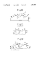
- FIG. 1 is a cross-sectional view of a liquid crystal display device according to the embodiment of the present invention.
- FIG. 2 is a plan view illustrating the arrangement of four liquid crystal display panels of FIG. 1;
- FIGS. 3A to 3C are views illustrating the feature of one of the convergently transmissive elements of FIG. 1;
- FIG. 4 is a view illustrating the propagation of light in the convergently transmissive element
- FIG. 5 is a view illustrating formation of an erect and real image having an identical size to an object
- FIG. 6 is a diagrammatic perspective view of an array of convergently transmissive elements of FIG. 1;
- FIG. 7 is a view illustrating the imaging surface and how the resolving power is reduced
- FIG. 8 is a cross-sectional view of the fresnel lens of FIG. 1;
- FIG. 9 is a partial plan view of the fresnel lens of FIG. 8.
- FIG. 10 is a cross-sectional view of a portion of the fresnel lens of FIGS. 8 and 9;
- FIG. 11 is a cross-sectional view of a conventional fresnel lens
- FIG. 12 is similar to FIG. 10, but includes several dimensional characters for calculating the width of the shading layer on the flat crest of the ridge of the configured surface of the fresnel lens;
- FIG. 13 is a plan view of the modified liquid crystal display panels
- FIG. 14 is a view illustrating the pictures produced by the main display area and the peripheral compensating area of the liquid crystal display panel
- FIG. 15 is a view illustrating the image on the screen produced by two adjacent liquid crystal display panels
- FIG. 16 is a view illustrating the pictures produced by the main display area and the image of the peripheral compensating area of the liquid crystal display panel of FIG. 15;
- FIG. 18 is a cross-sectional view illustrating the course of light emerging from the main display area and the peripheral compensating area to the screen;
- FIG. 19 is a plan view illustrating an element of an image on a screen
- FIG. 20 is a plan view of several elements of an image on a screen.
- FIG. 21 is a view illustrating how the brightness of the image at the peripheral region of the screen is reduced.
- FIGS. 1 and 2 show the liquid crystal display device 10 according to the present invention.
- the liquid crystal display device 10 includes four liquid crystal display panels 12 which are arranged in respective quarter portions in a rectangular region.
- Each liquid crystal display panel 12 includes an effective display region 12a and a non-display region 12b around the effective display region 12a, the non-display region 12b being necessary for attaching a drive circuit or the like to the panel for driving the liquid crystal in the panel. Therefore, an image is not formed on the non-display region 12b and a discontinuous image is formed if four liquid crystal display panels 12 are directly seen.
- the embodiment realizes a continuous multi-display from discontinuous images from four liquid crystal display panels 12, by providing a magnifying element.
- the liquid crystal display device 10 includes a backlight 14 on the rear side of the panels 12, and arrays 16 of convergently transmissive elements on the front side of the respective panels 12.
- the area of each of the arrays 16 of convergently transmissive elements is larger than the area of the effective display region 12a, but smaller than the total area of the panel 12 including the non-display region 12b.
- Each array 16 of convergently transmissive elements can form an erect and real image having an identical size to an object, i.e., an image produced by the liquid crystal display panel 12.
- the liquid crystal display device 10 includes fresnel lenses 18 on the output side of the arrays 16 of convergently transmissive elements, respectively.
- Each fresnel lens 18 includes a transparent body having a flat surface 18a and a configured surface 18b, in a saw-shape in cross-section, with concentrically periodic ridges 19, as shown in FIGS. 8 and 9.
- the fresnel lens 18 is arranged such that light is mainly incident onto the configured surface 18b of the fresnel lens 18.
- the configured surface 18b faces the array 16.
- the flat surface 18a is thus arranged on the light emerging side.
- the liquid crystal display device 10 also includes a screen 22 having a screen fresnel lens 20 on the front side of the fresnel lenses 18. Light beams emerging from the fresnel lenses 18 divergently travel toward the screen 22 so that light beams emerging from the adjacent fresnel lenses 18 meet on the screen 22 without a discontinuity. Therefore, the non-display regions 12b of the liquid crystal display panels 12 cannot be seen by a person watching the screen 22.
- the liquid crystal display panels 12 are one example of an image modulating means, and other types of image modulating means, which merge light, can be used.
- the array 16 comprises a plurality of convergently transmissive elements 16a and the features of one of the convergently transmissive elements 16a is shown in FIGS. 3A to 3C.
- the convergently transmissive element 16a is made from plastic or glass in the form of transparent rod having the diameter of 1 mm to 2 mm.
- the refractive index of the element 16a changes in the body thereof in the radial direction, as shown in FIG. 3C.
- the distribution of refractive index n(r) is represented by the following quadratic function
- n O refractive index on the vertical axis
- g is a distribution constant of the refractive index
- the distance L is the distance between the object and the image.
- FIG. 6 shows that the convergently transmissive elements 16a are arranged in a close relationship to each other with the end surfaces thereof arranged in a line or in a plane, to thereby form the array 16.
- An erect and real image having an identical size to an object can be formed by the array 16.
- the imaging device using the array 16 of convergently transmissive elements 16a offers advantages in that a focal distance is very short, and the optical performance is uniform in the line or plane.
- the array 16 of convergently transmissive elements 16a can be used only as a full size imaging device, and the fresnel lenses 18 are used as a magnifying means.
- the area of the effective region 12a of the liquid crystal display panel 12 is 211.2 mm ⁇ 158.4 mm, and the required magnification (a value of the sum of the area of the effective region 12a and the area of the ineffective region 12 divided by the area of the effective region 12a) is 1.09.
- the refractive index n is 1.507
- the distribution constant of refractive index g is 0.1847
- the length Z is 18.89 mm
- the diameter is 1.18 mm.
- the magnifying fresnel lens 18 is made from acryl having refractive index of 1.494 and has a radius of curvature in which the central curvature (cuy) is -0.00813668, the secondary constant is -0.775202 ⁇ 10 -8 , the tertiary constant is 0.318549 ⁇ 10 -13 , the quartic constant is -0.720974 ⁇ 10 -19 , and the quintic constant is -0.717576 ⁇ 10 -25 .
- the angle (AEP) of light emerging from the outermost peripheral position of the fresnel lens 18 relative to the normal line of the fresnel lens 18 is 28.3 degrees.
- the screen fresnel lens 20 serves to convert light beams emerging from the magnifying fresnel lens 18 with a variety of angles into parallel light beams, and is made from MS having refractive index of 1.537.
- the resolving power MTF in this example is shown in the following table.
- the shape of the configured surface 18b of the fresnel lens 18 is changed so that the angle (AEP) of light emerging from the outermost peripheral position of the fresnel lens 18 is changed.
- the resolving power MTF is examined while changing the angle (AEP).
- the refractive index n of the convergently transmissive elements 16a is 1.505
- the distribution constant of the refractive index g is 0.1847
- the length Z is 18.895 mm
- the distance L is 20 mm.
- the thickness of the fresnel lens 18 is 2 mm and refractive index is 1.494.
- the fresnel lens 18 is arranged to contact the array 16 of convergently transmissive elements 16a.
- the curvature of the fresnel lens 18 is set in a parabolic shape so that a light beam (referred to as the main light beam) parallel to the optical axis of the fresnel lens 18 emerges from the outermost peripheral position of the fresnel lens 18 at an angle (AEP), and the focal point is at a position on a line passing through the center of the fresnel lens 18.
- the resolving power MTF in this example is shown in the following table. It should be noted that the configured surface 18b is on the light incident side and the flat surface 18a is on the light emerging side.
- the following table shows the result of a test regarding resolving power MTF obtained when the flat surface 18a is on the light incident side and the configured surface 18b is on the light emerging side and the other conditions are similar to those of the above example. This result should be compared with resolving force MTF obtained when the configured surface 18b is on the light incident side and the flat surface 18a is on the light emerging side.
- the inventors further tried to analyze the reason why the resolving power MTF is reduced when the flat surface 18a is on the light incident side and the configured surface 18b is on the light emerging side.
- the focal length of the fresnel lens 18 becomes shorter as the position is displaced from the center of the fresnel lens 18 to the periphery thereof, and an imaging surface is distorted relative to the screen 22 as shown by the broken line F.
- the array 16 of the convergently transmissive elements 16a and the fresnel lens 18 are shown, but the fresnel lens 18 is arranged such that the configured surface 18b is on the light emerging side.
- the angle (AIM) between light beams 30 and 31 which are inclined to the main light beam on either side of the main light beam at identical angles relative to the main light beam is noted.
- the angle (AIM) between light beams 30 and 31 becomes smaller when light is made incident to the fresnel lens 18, and the angle (AIM) becomes greater when light emerges from the fresnel lens 18, regardless of which surface is on the light incident side. This tendency is stronger as the angle between the incident or merging light and the incident or emerging surface becomes greater, that is, this tendency is stronger with respect to the configured surface 18b.
- the angle (AIM) between light beams 30 and 31 becomes greater in the arrangement where light emerges from the configured surface 18b, and an image is formed far from the screen 22 as the angle (AIM) becomes greater, with the result that resolving power MTF is reduced.
- the angle (AIM) does not become so greater in the arrangement where light emerges from the flat surface 18a, and in this case, it is possible to form an image on the screen 22.
- FIG. 10 shows the details of the fresnel lens 18 of FIG. 1.
- the fresnel lens 18 has the flat surface 18a and the configured surface 18b with concentrically periodic ridges 19.
- Each of the ridges 19 includes a flat; crest 19a extending generally parallel to the flat surface 18a and an inclined surface 19b extending from the flat crest 19a toward the flat surface 18a.
- a minor surface 19c which is perpendicular to the flat surface 18a in FIG. 10 is arranged on the opposite side of the flat crest 19a from the inclined surface 19b.
- a shading layer 19d is provided on the flat crest 19a of each of the ridges 19. The shading layer 19d can be easily formed by printing since the flat crest 19a is parallel to the flat surface 18a.
- FIG. 11 shows a conventional fresnel lens 18 having ridges 19. It will be understood that the flat crest 19a of FIG. 10 is formed by cutting the apex of the ridge 19 of FIG. 10.
- the conventional fresnel lens 18 shown in FIG. 10 there is a problem of a straying beam inducing a ghost. That is, if light S is made incident to the inclined surface 19b at a position near the surface 19c, light S is reflected by the minor surface 19c and changes its course in an uncontrolled direction to thereby induce a ghost.
- the shading layer 19d is provided to solve this problem.
- the shape or the slope of the ridges 19 changes depending on the positions of the ridges 19, and it is preferable that the flat crests 19d have varying widths depending on the positions of the ridges 19.
- the surface 19c may be inclined relative to the flat surface 18a for the reason of fabrication of the fresnel lens 18.
- the main inclined surface 19b arranged on one side of the flat crest 19a is designed such that light is mainly incident to the body of the fresnel lens 18 from the main inclined surface 19b, and the minor inclined surface 19c is arranged on the other side of the flat crest 19a from the main inclined surface 19b.
- the width of the flat crest 19a is determined by the following relationship: ##EQU2## where d is the width of the flat crest 19a, p is the pitch of the ridges 19, r is the angle of a major light ray made incident to the body from the main inclined surface 19a relative to the axis, ⁇ 1 is the angle the main inclined surface 19b relative to the flat surface 18a, and ⁇ 2 is the angle of the minor inclined surface 19c relative to the axis of the fresnel lens 18.
- FIGS. 13, 17 and 18 show the modified liquid crystal display device 10, which includes four sets of the liquid crystal display panels 12, the arrays 16 of convergently transmissive elements 16a and the fresnel lenses 18, and a screen 22.
- the four sets are arranged in respective quarter portions in a rectangular region.
- the screen 22 has a total display area four times greater than a predetermined display area 22p necessary to receive an image from one set of the liquid crystal display panel 12, the array 16 of convergently transmissive elements and the fresnel lens 18. That is, the screen 22 has a predetermined display area 22p for each of the liquid crystal display panel 12.
- a partition 26 is arranged on or near the screen 22 between two adjacent sets of the liquid crystal display panels 12, the arrays 16 of convergently transmissive elements and the fresnel lenses 18 for preventing light from straying from one set into the adjacent set.
- Each liquid crystal display panel 12 includes an effective display region 12a and a non-display region 12b around the effective display region 12a, as described with reference to FIG. 2.
- the effective display region 12a is further divided into a main display area 12x and a peripheral compensating area 12y.
- the main display area 12x forms an image on the predetermined display area 22p via the array 16 of convergently transmissive elements and the fresnel lens 18.
- the peripheral compensating area 12y forms an image just outside the predetermined display area 22p via the array 16 of convergently transmissive elements and the fresnel lens 18.
- the peripheral compensating area 12y does not contribute to the formation of the actual image on the screen 22, but compensates for a loss in brightness in the peripheral region of the liquid crystal display panel 12.
- the effective display region 12a includes 640 ⁇ 480 pixels
- the main display area 12x includes 620 ⁇ 465 pixels.
- the peripheral compensating area 12y of the liquid crystal display panel 12 is controlled to provide an image I 1 which is generally identical to a portion I 1 of an image delivered from the main display area 12x of the liquid crystal display panel 12 near the peripheral compensating area 12y.
- the peripheral compensating area 12y of the liquid crystal display panel 12 is controlled to provide an image I 2 which is generally identical to a portion I 2 of an image delivered from the main display area 12x of the adjacent liquid crystal display panel 12 near the peripheral compensating area 12y of said one liquid crystal display panel 12.
- FIG. 19 shows an element 50 of an image on a screen 22.
- the element 50 should be a point at which several light beams are focussed, but in fact, light beams may scatter to a certain region 51 due to an aberration of the magnifying fresnel lens 18. Therefore, brightness of the element 50 may be reduced.
- FIG. 20 shows several elements 50, 50a, 50b, 50c, and 50d, with their scattering regions 51, 51a, 51b, 51c, and 51d.
- the element 50 receives light from the other elements 50a, 50b, 50c, and 50d and brightness of the element 50 may be compensated to some extent.
- FIG. 21 shows a peripheral portion of the screen 22 when the peripheral compensating area 12y is not provided.
- the peripheral compensating area 12y produces light outside the predetermined display area 22p and does not contribute to the formation of an actual image, but light emerged from the peripheral compensating area 12y may include scattered light components which compensate for the reduced brightness on the peripheral portion of the screen 22.
Landscapes
- Physics & Mathematics (AREA)
- General Physics & Mathematics (AREA)
- Optics & Photonics (AREA)
- Nonlinear Science (AREA)
- Chemical & Material Sciences (AREA)
- Crystallography & Structural Chemistry (AREA)
- Mathematical Physics (AREA)
- Engineering & Computer Science (AREA)
- Theoretical Computer Science (AREA)
- Liquid Crystal (AREA)
Priority Applications (5)
| Application Number | Priority Date | Filing Date | Title |
|---|---|---|---|
| US08/508,632 US5751387A (en) | 1995-07-28 | 1995-07-28 | Fresnel lens and liquid crystal display device |
| FR9509514A FR2737581B1 (fr) | 1995-07-28 | 1995-08-04 | Lentille de fresnel et dispositif d'affichage a cristaux liquides |
| FR9514847A FR2737595B1 (fr) | 1995-07-28 | 1995-12-14 | Dispositif d'affichage a cristaux liquides |
| US08/948,624 US6380994B1 (en) | 1995-07-28 | 1997-10-10 | Fresnel lens and liquid crystal display device |
| US09/548,086 US6211932B1 (en) | 1995-07-28 | 2000-04-11 | Fresnel lens and liquid crystal display device |
Applications Claiming Priority (3)
| Application Number | Priority Date | Filing Date | Title |
|---|---|---|---|
| US08/508,632 US5751387A (en) | 1995-07-28 | 1995-07-28 | Fresnel lens and liquid crystal display device |
| FR9509514A FR2737581B1 (fr) | 1995-07-28 | 1995-08-04 | Lentille de fresnel et dispositif d'affichage a cristaux liquides |
| FR9514847A FR2737595B1 (fr) | 1995-07-28 | 1995-12-14 | Dispositif d'affichage a cristaux liquides |
Related Child Applications (1)
| Application Number | Title | Priority Date | Filing Date |
|---|---|---|---|
| US08/948,624 Division US6380994B1 (en) | 1995-07-28 | 1997-10-10 | Fresnel lens and liquid crystal display device |
Publications (1)
| Publication Number | Publication Date |
|---|---|
| US5751387A true US5751387A (en) | 1998-05-12 |
Family
ID=27253088
Family Applications (1)
| Application Number | Title | Priority Date | Filing Date |
|---|---|---|---|
| US08/508,632 Expired - Lifetime US5751387A (en) | 1995-07-28 | 1995-07-28 | Fresnel lens and liquid crystal display device |
Country Status (2)
| Country | Link |
|---|---|
| US (1) | US5751387A (fr) |
| FR (1) | FR2737595B1 (fr) |
Cited By (24)
| Publication number | Priority date | Publication date | Assignee | Title |
|---|---|---|---|---|
| US6014232A (en) * | 1996-09-07 | 2000-01-11 | U.S. Philips Corporation | Electrical device comprising an array of pixels |
| WO2000016132A1 (fr) * | 1998-09-15 | 2000-03-23 | Peter Milner | Reseau prismatique pour retroviseur |
| US6046847A (en) * | 1997-04-11 | 2000-04-04 | Dai Nippon Printing Co., Ltd. | Rear projection screen containing Fresnel lens sheet utilizing alternative focal lengths |
| WO2000041009A1 (fr) * | 1998-12-31 | 2000-07-13 | Microsharp Corporation Limited | Diffuseur a surface crenelee |
| US6151162A (en) * | 1997-12-29 | 2000-11-21 | U.S. Philips Corporation | Rear projection screen |
| WO2000070404A1 (fr) * | 1999-05-14 | 2000-11-23 | Microsharp Corporation Limited | Dispositif d'affichage et plaque de transmission de lumiere pour dispositif d'affichage |
| US6211932B1 (en) | 1995-07-28 | 2001-04-03 | Fujitsu Limited | Fresnel lens and liquid crystal display device |
| EP1089094A1 (fr) * | 1999-09-30 | 2001-04-04 | Valeo Vision | Procédé de fabrication d'éléments dioptriques et éléments dioptriques pour dispositif d'éclairage. |
| US20010035926A1 (en) * | 2000-02-29 | 2001-11-01 | Akira Yamaguchi | Light diffusing plate and display apparatus |
| US6344928B1 (en) * | 1998-10-23 | 2002-02-05 | Kabushiki Kaisha Toshiba | Display device |
| WO2002008796A3 (en) * | 2000-07-25 | 2002-04-25 | Scram Technologies Inc | Black serrated optical panel |
| US6407859B1 (en) * | 1999-01-13 | 2002-06-18 | 3M Innovative Properties Company | Fresnel lens for projection screen |
| EP1291709A1 (fr) * | 2001-02-14 | 2003-03-12 | Arisawa Optics Co., Ltd. | Ecran de projection a reflexion |
| US20030231144A1 (en) * | 2002-06-17 | 2003-12-18 | Samsung Electronics Co., Ltd. | Multi-display apparatus having an optical path changing device |
| US6667786B2 (en) * | 2000-12-12 | 2003-12-23 | Koninklijke Philips Electronics N.V. | Display device and lenticular screen |
| US6670205B1 (en) * | 2002-09-18 | 2003-12-30 | Hynix Semiconductor Inc | Method of fabricating image sensor equipped with lens |
| US6814578B2 (en) | 2002-04-11 | 2004-11-09 | The Boeing Company | Visual display system and method for displaying images utilizing a holographic collimator |
| US20050141087A1 (en) * | 2002-03-28 | 2005-06-30 | Dai Nippon Printing Co., Ltd. | Fresnel lens sheet |
| US20050254130A1 (en) * | 2002-02-22 | 2005-11-17 | Wolfgang Graf | Device for guiding light |
| US20060227433A1 (en) * | 2003-12-17 | 2006-10-12 | Hiroshi Suzuki | Fresnel optical element and projection display device |
| US20090207096A1 (en) * | 2008-02-19 | 2009-08-20 | Seung-Chul Lee | Multi panel display device |
| US20110080665A1 (en) * | 2009-10-05 | 2011-04-07 | Delphi Technologies, Inc. | Visual gap mitigation apparatus for a segmented display panel |
| US20120139964A1 (en) * | 2010-12-03 | 2012-06-07 | Samsung Electronics Co., Ltd. | Display panel module and multi-panel display apparatus including the same |
| EP3639068A4 (fr) * | 2017-07-20 | 2020-07-01 | Wavefront Technology, Inc. | Lentilles de fresnel ultra-minces et autres éléments optiques |
Families Citing this family (1)
| Publication number | Priority date | Publication date | Assignee | Title |
|---|---|---|---|---|
| FR2815137A1 (fr) * | 2000-10-05 | 2002-04-12 | Gwenole Bocquet | Elargissement d'angle pour projection virtuelle |
Citations (28)
| Publication number | Priority date | Publication date | Assignee | Title |
|---|---|---|---|---|
| US3004470A (en) * | 1956-07-28 | 1961-10-17 | Zeiss Ikon A G Stuttgart | Multiple focal length lens |
| US3784282A (en) * | 1971-03-05 | 1974-01-08 | Hitachi Ltd | Correcting lens used to form fluorescent screens of colour television receiving tubes |
| JPS5833526A (ja) * | 1981-08-25 | 1983-02-26 | Tochigi Fuji Ind Co Ltd | クラツチを備えた四輪駆動車 |
| JPS5837630A (ja) * | 1981-08-31 | 1983-03-04 | Dainippon Printing Co Ltd | 透過型スクリ−ン及びその製造法 |
| JPS58122527A (ja) * | 1982-01-18 | 1983-07-21 | Hitachi Ltd | 背面投写スクリ−ンおよびこれを用いた背面投写装置 |
| US4408836A (en) * | 1980-02-28 | 1983-10-11 | Sharp Kabushiki Kaisha | Wide screen LCD panel with electrical terminal connections |
| JPS60227233A (ja) * | 1984-04-25 | 1985-11-12 | Matsushita Electric Ind Co Ltd | 平面画像表示パネル装置 |
| JPS6112249A (ja) * | 1984-06-26 | 1986-01-20 | Okayamaken | 米粉クレ−プと米粉ワツフル |
| JPS62180755A (ja) * | 1986-01-31 | 1987-08-08 | 日本精機株式会社 | 防眩機能を有する透視板 |
| JPS62200302A (ja) * | 1986-02-27 | 1987-09-04 | Nippon Seiki Co Ltd | 自発光型表示装置における表示面反射の視野外除去方法 |
| JPS62201401A (ja) * | 1986-02-28 | 1987-09-05 | Nippon Seiki Co Ltd | 防眩機能を有する透視板 |
| US4756603A (en) * | 1986-01-31 | 1988-07-12 | Nippon Seiki Co., Ltd. | Glare-proof transparent cover plate |
| EP0312341A2 (fr) * | 1987-10-13 | 1989-04-19 | Theodore Robert Whitney | Systèmes de formation d'image de haute résolution |
| US4936657A (en) * | 1985-07-18 | 1990-06-26 | Asahi Kogaku Kogyo Kabushiki Kaisha | Projection type liquid-crystal video display device using a fresnel lens |
| US5066099A (en) * | 1989-04-26 | 1991-11-19 | Hitachi, Ltd. | Rear projection screen and method of producing the same |
| US5191479A (en) * | 1991-03-28 | 1993-03-02 | Nipox Kabushiki Kaisha | Fresnel lens |
| US5191472A (en) * | 1988-11-29 | 1993-03-02 | Canon Kabushiki Kaisha | Apparatus having a screen with light blocking elements |
| US5206761A (en) * | 1991-03-27 | 1993-04-27 | Hitachi, Ltd. | Large-screen projection type display |
| JPH05188340A (ja) * | 1992-01-09 | 1993-07-30 | Fujitsu Ltd | 投写型表示装置 |
| US5268879A (en) * | 1991-12-03 | 1993-12-07 | Raytheon Company | Electro-acostic transducers |
| EP0581221A1 (fr) * | 1992-07-31 | 1994-02-02 | Nippon Telegraph And Telephone Corporation | Dispositif d'affichage et de capture d'image |
| US5355187A (en) * | 1992-03-13 | 1994-10-11 | Hitachi, Ltd. | Liquid crystal projection display |
| US5371617A (en) * | 1991-10-15 | 1994-12-06 | Canon Kabushiki Kaisha | Liquid crystal projector with one modulator including a member for preventing light from another modulator from entering the one |
| US5398125A (en) * | 1993-11-10 | 1995-03-14 | Minnesota Mining And Manufacturing Company | Liquid crystal projection panel having microlens arrays, on each side of the liquid crystal, with a focus beyond the liquid crystal |
| EP0645661A1 (fr) * | 1993-09-28 | 1995-03-29 | Minnesota Mining And Manufacturing Company | Panneau de projection à cristaux liquides |
| US5426531A (en) * | 1992-12-14 | 1995-06-20 | Mitsubishi Denki Kabushiki Kaisha | Transmission screen |
| US5434706A (en) * | 1991-11-15 | 1995-07-18 | Matsushita Electric Industrial Co., Ltd. | Transmission type screen and method of manufacturing thereof |
| US5504597A (en) * | 1992-06-17 | 1996-04-02 | Xerox Corporation | Full color display with gradient index lens array disposed between phosphor emitters and liquid crystal display |
-
1995
- 1995-07-28 US US08/508,632 patent/US5751387A/en not_active Expired - Lifetime
- 1995-12-14 FR FR9514847A patent/FR2737595B1/fr not_active Expired - Fee Related
Patent Citations (29)
| Publication number | Priority date | Publication date | Assignee | Title |
|---|---|---|---|---|
| US3004470A (en) * | 1956-07-28 | 1961-10-17 | Zeiss Ikon A G Stuttgart | Multiple focal length lens |
| US3784282A (en) * | 1971-03-05 | 1974-01-08 | Hitachi Ltd | Correcting lens used to form fluorescent screens of colour television receiving tubes |
| US4408836A (en) * | 1980-02-28 | 1983-10-11 | Sharp Kabushiki Kaisha | Wide screen LCD panel with electrical terminal connections |
| JPS5833526A (ja) * | 1981-08-25 | 1983-02-26 | Tochigi Fuji Ind Co Ltd | クラツチを備えた四輪駆動車 |
| JPS5837630A (ja) * | 1981-08-31 | 1983-03-04 | Dainippon Printing Co Ltd | 透過型スクリ−ン及びその製造法 |
| JPS58122527A (ja) * | 1982-01-18 | 1983-07-21 | Hitachi Ltd | 背面投写スクリ−ンおよびこれを用いた背面投写装置 |
| JPS60227233A (ja) * | 1984-04-25 | 1985-11-12 | Matsushita Electric Ind Co Ltd | 平面画像表示パネル装置 |
| JPS6112249A (ja) * | 1984-06-26 | 1986-01-20 | Okayamaken | 米粉クレ−プと米粉ワツフル |
| US4936657A (en) * | 1985-07-18 | 1990-06-26 | Asahi Kogaku Kogyo Kabushiki Kaisha | Projection type liquid-crystal video display device using a fresnel lens |
| JPS62180755A (ja) * | 1986-01-31 | 1987-08-08 | 日本精機株式会社 | 防眩機能を有する透視板 |
| US4756603A (en) * | 1986-01-31 | 1988-07-12 | Nippon Seiki Co., Ltd. | Glare-proof transparent cover plate |
| JPS62200302A (ja) * | 1986-02-27 | 1987-09-04 | Nippon Seiki Co Ltd | 自発光型表示装置における表示面反射の視野外除去方法 |
| JPS62201401A (ja) * | 1986-02-28 | 1987-09-05 | Nippon Seiki Co Ltd | 防眩機能を有する透視板 |
| EP0312341A2 (fr) * | 1987-10-13 | 1989-04-19 | Theodore Robert Whitney | Systèmes de formation d'image de haute résolution |
| US5191472A (en) * | 1988-11-29 | 1993-03-02 | Canon Kabushiki Kaisha | Apparatus having a screen with light blocking elements |
| US5066099A (en) * | 1989-04-26 | 1991-11-19 | Hitachi, Ltd. | Rear projection screen and method of producing the same |
| US5206761A (en) * | 1991-03-27 | 1993-04-27 | Hitachi, Ltd. | Large-screen projection type display |
| US5191479A (en) * | 1991-03-28 | 1993-03-02 | Nipox Kabushiki Kaisha | Fresnel lens |
| US5371617A (en) * | 1991-10-15 | 1994-12-06 | Canon Kabushiki Kaisha | Liquid crystal projector with one modulator including a member for preventing light from another modulator from entering the one |
| US5434706A (en) * | 1991-11-15 | 1995-07-18 | Matsushita Electric Industrial Co., Ltd. | Transmission type screen and method of manufacturing thereof |
| US5268879A (en) * | 1991-12-03 | 1993-12-07 | Raytheon Company | Electro-acostic transducers |
| JPH05188340A (ja) * | 1992-01-09 | 1993-07-30 | Fujitsu Ltd | 投写型表示装置 |
| US5355187A (en) * | 1992-03-13 | 1994-10-11 | Hitachi, Ltd. | Liquid crystal projection display |
| US5504597A (en) * | 1992-06-17 | 1996-04-02 | Xerox Corporation | Full color display with gradient index lens array disposed between phosphor emitters and liquid crystal display |
| US5504598A (en) * | 1992-06-17 | 1996-04-02 | Xerox Corporation | Large screen full color display with plural adjacent display panels and enlarging graded index lens array |
| EP0581221A1 (fr) * | 1992-07-31 | 1994-02-02 | Nippon Telegraph And Telephone Corporation | Dispositif d'affichage et de capture d'image |
| US5426531A (en) * | 1992-12-14 | 1995-06-20 | Mitsubishi Denki Kabushiki Kaisha | Transmission screen |
| EP0645661A1 (fr) * | 1993-09-28 | 1995-03-29 | Minnesota Mining And Manufacturing Company | Panneau de projection à cristaux liquides |
| US5398125A (en) * | 1993-11-10 | 1995-03-14 | Minnesota Mining And Manufacturing Company | Liquid crystal projection panel having microlens arrays, on each side of the liquid crystal, with a focus beyond the liquid crystal |
Cited By (42)
| Publication number | Priority date | Publication date | Assignee | Title |
|---|---|---|---|---|
| US6211932B1 (en) | 1995-07-28 | 2001-04-03 | Fujitsu Limited | Fresnel lens and liquid crystal display device |
| US6380994B1 (en) * | 1995-07-28 | 2002-04-30 | Fujitsu Limited | Fresnel lens and liquid crystal display device |
| US6014232A (en) * | 1996-09-07 | 2000-01-11 | U.S. Philips Corporation | Electrical device comprising an array of pixels |
| US6046847A (en) * | 1997-04-11 | 2000-04-04 | Dai Nippon Printing Co., Ltd. | Rear projection screen containing Fresnel lens sheet utilizing alternative focal lengths |
| US6151162A (en) * | 1997-12-29 | 2000-11-21 | U.S. Philips Corporation | Rear projection screen |
| WO2000016132A1 (fr) * | 1998-09-15 | 2000-03-23 | Peter Milner | Reseau prismatique pour retroviseur |
| GB2342726A (en) * | 1998-09-15 | 2000-04-19 | Milner Peter J | Optical component |
| GB2342726B (en) * | 1998-09-15 | 2003-03-12 | Milner Peter J | A light transmission optical component with degraded crests for reducing flare |
| US6344928B1 (en) * | 1998-10-23 | 2002-02-05 | Kabushiki Kaisha Toshiba | Display device |
| WO2000041009A1 (fr) * | 1998-12-31 | 2000-07-13 | Microsharp Corporation Limited | Diffuseur a surface crenelee |
| US6710941B2 (en) | 1999-01-13 | 2004-03-23 | 3M Innovative Properties Company | Fresnel lens for projection screens |
| US6407859B1 (en) * | 1999-01-13 | 2002-06-18 | 3M Innovative Properties Company | Fresnel lens for projection screen |
| WO2000070404A1 (fr) * | 1999-05-14 | 2000-11-23 | Microsharp Corporation Limited | Dispositif d'affichage et plaque de transmission de lumiere pour dispositif d'affichage |
| FR2799268A1 (fr) * | 1999-09-30 | 2001-04-06 | Valeo Vision | Procede de fabrication d'elements dioptriques et elements dioptriques pour dispositif d'eclairage |
| EP1089094A1 (fr) * | 1999-09-30 | 2001-04-04 | Valeo Vision | Procédé de fabrication d'éléments dioptriques et éléments dioptriques pour dispositif d'éclairage. |
| US20010035926A1 (en) * | 2000-02-29 | 2001-11-01 | Akira Yamaguchi | Light diffusing plate and display apparatus |
| US20090009701A1 (en) * | 2000-02-29 | 2009-01-08 | Akira Yamaguchi | Light Diffusing Plate and Display Apparatus |
| WO2002008796A3 (en) * | 2000-07-25 | 2002-04-25 | Scram Technologies Inc | Black serrated optical panel |
| US6597417B1 (en) | 2000-07-25 | 2003-07-22 | Scram Technologies, Inc. | Optical panel having black material between apexes of serrations on the inlet face |
| US6667786B2 (en) * | 2000-12-12 | 2003-12-23 | Koninklijke Philips Electronics N.V. | Display device and lenticular screen |
| US20030137728A1 (en) * | 2001-02-14 | 2003-07-24 | Kazumi Kuroda | Reflection projection screen |
| EP1291709A4 (fr) * | 2001-02-14 | 2003-05-28 | Arisawa Optics Co Ltd | Ecran de projection a reflexion |
| CN100334503C (zh) * | 2001-02-14 | 2007-08-29 | 株式会社有泽制作所 | 反射型投影屏幕 |
| EP1291709A1 (fr) * | 2001-02-14 | 2003-03-12 | Arisawa Optics Co., Ltd. | Ecran de projection a reflexion |
| US6842282B2 (en) | 2001-02-14 | 2005-01-11 | Arisawa Mfg. Co., Ltd. | Reflection projection screen |
| US20050254130A1 (en) * | 2002-02-22 | 2005-11-17 | Wolfgang Graf | Device for guiding light |
| US7173761B2 (en) * | 2002-03-28 | 2007-02-06 | Dai Nippon Printing Co., Ltd. | Fresnel lens sheet |
| US20050141087A1 (en) * | 2002-03-28 | 2005-06-30 | Dai Nippon Printing Co., Ltd. | Fresnel lens sheet |
| US6814578B2 (en) | 2002-04-11 | 2004-11-09 | The Boeing Company | Visual display system and method for displaying images utilizing a holographic collimator |
| US7439938B2 (en) * | 2002-06-17 | 2008-10-21 | Samsung Electronics Co., Ltd. | Multi-display apparatus having an optical path changing device |
| EP1376199A1 (fr) * | 2002-06-17 | 2004-01-02 | Samsung Electronics Co., Ltd. | Appareil multi-écrans comportant un dispositif modifiant le chemin optique |
| US20030231144A1 (en) * | 2002-06-17 | 2003-12-18 | Samsung Electronics Co., Ltd. | Multi-display apparatus having an optical path changing device |
| US6670205B1 (en) * | 2002-09-18 | 2003-12-30 | Hynix Semiconductor Inc | Method of fabricating image sensor equipped with lens |
| US7242536B2 (en) * | 2003-12-17 | 2007-07-10 | Mitsubishi Denki Kabushiki Kaisha | Fresnel optical element and projection display device |
| US20060227433A1 (en) * | 2003-12-17 | 2006-10-12 | Hiroshi Suzuki | Fresnel optical element and projection display device |
| US20090207096A1 (en) * | 2008-02-19 | 2009-08-20 | Seung-Chul Lee | Multi panel display device |
| US8194000B2 (en) * | 2008-02-19 | 2012-06-05 | Lg Display Co., Ltd. | Multi panel display device |
| US20110080665A1 (en) * | 2009-10-05 | 2011-04-07 | Delphi Technologies, Inc. | Visual gap mitigation apparatus for a segmented display panel |
| EP2312378A1 (fr) | 2009-10-05 | 2011-04-20 | Delphi Technologies, Inc. | Appareil de réduction d'écart visuel pour un panneau d'affichage segmenté |
| US20120139964A1 (en) * | 2010-12-03 | 2012-06-07 | Samsung Electronics Co., Ltd. | Display panel module and multi-panel display apparatus including the same |
| EP3639068A4 (fr) * | 2017-07-20 | 2020-07-01 | Wavefront Technology, Inc. | Lentilles de fresnel ultra-minces et autres éléments optiques |
| US10795059B2 (en) | 2017-07-20 | 2020-10-06 | Wavefront Technology, Inc. | Ultra thin Fresnel lenses and other optical elements |
Also Published As
| Publication number | Publication date |
|---|---|
| FR2737595A1 (fr) | 1997-02-07 |
| FR2737595B1 (fr) | 1997-12-12 |
Similar Documents
| Publication | Publication Date | Title |
|---|---|---|
| US5751387A (en) | Fresnel lens and liquid crystal display device | |
| US6456436B2 (en) | Optical device | |
| EP0913728B1 (fr) | Ecran de projection | |
| KR0177648B1 (ko) | 프로젝터의 후면투사스크린 | |
| US6407860B1 (en) | Fresnel lens sheet | |
| EP0203646B1 (fr) | Elément optique d'agrandissement d'image, appareil d'affichage d'information comportant un tel élément et panneau d'affichage d'information comportant plusieurs de ces appareils | |
| EP1632809A1 (fr) | Écran de projection comportant un réseau de micro-lentilles | |
| EP0864897A2 (fr) | Dispositif de source de lumière, système d'éclairage et projecteur d'images | |
| JPH09105804A (ja) | 光制御シート、面光源装置及び液晶表示装置 | |
| CN113436560A (zh) | 成像光学系统及显示装置 | |
| US6211932B1 (en) | Fresnel lens and liquid crystal display device | |
| JPS62226778A (ja) | リアプロジユクシヨン装置 | |
| EP0082714B1 (fr) | Ecran de projection arrière | |
| US5241416A (en) | Screen and projector using said screen | |
| JPH10301110A (ja) | 画像表示装置 | |
| US7287881B2 (en) | Light deflector and rear-projection screen | |
| KR100217489B1 (ko) | 프레넬 렌즈 및 액정 표시장치 | |
| KR19990012816A (ko) | 투사 스크린 | |
| KR100396128B1 (ko) | 액정표시장치 | |
| JP3485397B2 (ja) | 表示装置 | |
| US6603604B2 (en) | Screen for projection television | |
| KR100553889B1 (ko) | 프로젝션 표시 장치용 스크린 | |
| JP3390254B2 (ja) | 結像装置及び液晶表示装置 | |
| JPH09218465A (ja) | スクリーン装置 | |
| JP2001183601A (ja) | 画像投影装置 |
Legal Events
| Date | Code | Title | Description |
|---|---|---|---|
| AS | Assignment |
Owner name: FUJITSU, LIMITED, JAPAN Free format text: ASSIGNMENT OF ASSIGNORS INTEREST;ASSIGNORS:IIGAHAMA, YUKIO;FUKUHARA, MOTOHIKO;REEL/FRAME:007602/0781 Effective date: 19950724 |
|
| STCF | Information on status: patent grant |
Free format text: PATENTED CASE |
|
| FEPP | Fee payment procedure |
Free format text: PAYOR NUMBER ASSIGNED (ORIGINAL EVENT CODE: ASPN); ENTITY STATUS OF PATENT OWNER: LARGE ENTITY |
|
| CC | Certificate of correction | ||
| FPAY | Fee payment |
Year of fee payment: 4 |
|
| FPAY | Fee payment |
Year of fee payment: 8 |
|
| AS | Assignment |
Owner name: INTELLECTUAL VENTURES HOLDING 45 LLC, NEVADA Free format text: ASSIGNMENT OF ASSIGNORS INTEREST;ASSIGNOR:FUJITSU LIMITED;REEL/FRAME:020704/0550 Effective date: 20080221 |
|
| FEPP | Fee payment procedure |
Free format text: PAYOR NUMBER ASSIGNED (ORIGINAL EVENT CODE: ASPN); ENTITY STATUS OF PATENT OWNER: LARGE ENTITY Free format text: PAYER NUMBER DE-ASSIGNED (ORIGINAL EVENT CODE: RMPN); ENTITY STATUS OF PATENT OWNER: LARGE ENTITY |
|
| FPAY | Fee payment |
Year of fee payment: 12 |
|
| AS | Assignment |
Owner name: INTELLECTUAL VENTURES I LLC, DELAWARE Free format text: MERGER;ASSIGNOR:INTELLECTUAL VENTURES HOLDING 45 LLC;REEL/FRAME:026637/0317 Effective date: 20110718 |