US5640097A - Test pattern for separately determining plug resistance and interfactial resistance - Google Patents
Test pattern for separately determining plug resistance and interfactial resistance Download PDFInfo
- Publication number
- US5640097A US5640097A US08/724,350 US72435096A US5640097A US 5640097 A US5640097 A US 5640097A US 72435096 A US72435096 A US 72435096A US 5640097 A US5640097 A US 5640097A
- Authority
- US
- United States
- Prior art keywords
- patterns
- resistance
- contact
- contact holes
- semiconductor region
- Prior art date
- Legal status (The legal status is an assumption and is not a legal conclusion. Google has not performed a legal analysis and makes no representation as to the accuracy of the status listed.)
- Expired - Fee Related
Links
Images


Classifications
-
- H—ELECTRICITY
- H01—ELECTRIC ELEMENTS
- H01L—SEMICONDUCTOR DEVICES NOT COVERED BY CLASS H10
- H01L22/00—Testing or measuring during manufacture or treatment; Reliability measurements, i.e. testing of parts without further processing to modify the parts as such; Structural arrangements therefor
-
- H—ELECTRICITY
- H01—ELECTRIC ELEMENTS
- H01L—SEMICONDUCTOR DEVICES NOT COVERED BY CLASS H10
- H01L22/00—Testing or measuring during manufacture or treatment; Reliability measurements, i.e. testing of parts without further processing to modify the parts as such; Structural arrangements therefor
- H01L22/30—Structural arrangements specially adapted for testing or measuring during manufacture or treatment, or specially adapted for reliability measurements
- H01L22/34—Circuits for electrically characterising or monitoring manufacturing processes, e. g. whole test die, wafers filled with test structures, on-board-devices incorporated on each die, process control monitors or pad structures thereof, devices in scribe line
-
- G—PHYSICS
- G01—MEASURING; TESTING
- G01R—MEASURING ELECTRIC VARIABLES; MEASURING MAGNETIC VARIABLES
- G01R31/00—Arrangements for testing electric properties; Arrangements for locating electric faults; Arrangements for electrical testing characterised by what is being tested not provided for elsewhere
- G01R31/26—Testing of individual semiconductor devices
- G01R31/2648—Characterising semiconductor materials
-
- G—PHYSICS
- G01—MEASURING; TESTING
- G01R—MEASURING ELECTRIC VARIABLES; MEASURING MAGNETIC VARIABLES
- G01R31/00—Arrangements for testing electric properties; Arrangements for locating electric faults; Arrangements for electrical testing characterised by what is being tested not provided for elsewhere
- G01R31/28—Testing of electronic circuits, e.g. by signal tracer
- G01R31/2851—Testing of integrated circuits [IC]
- G01R31/2884—Testing of integrated circuits [IC] using dedicated test connectors, test elements or test circuits on the IC under test
-
- H—ELECTRICITY
- H01—ELECTRIC ELEMENTS
- H01L—SEMICONDUCTOR DEVICES NOT COVERED BY CLASS H10
- H01L2924/00—Indexing scheme for arrangements or methods for connecting or disconnecting semiconductor or solid-state bodies as covered by H01L24/00
- H01L2924/0001—Technical content checked by a classifier
- H01L2924/0002—Not covered by any one of groups H01L24/00, H01L24/00 and H01L2224/00
Definitions
- the present invention relates to a test pattern for measuring an electric property in a semiconductor device and a test method using the test pattern, and more particularly, to a test pattern for measuring a contact resistance in a contact section and a test method using the test pattern.
- the pattern size section in a semiconductor device becomes fine as progress of semiconductor technology.
- the size of a contact hole also becomes fine.
- an interlayer insulating film has been sufficiently planarized so that workability can be sufficiently accomplished.
- the interlayer insulating film had a hollow surface in a portion for a contact hole to have been formed. Accordingly, the depth of the contact hole was shallower by the hollow portion than the other portion of the interlayer insulating film.
- the planarization of surface is made to remove any hollow portion so that the depth of the contact hole becomes deep.
- an aspect ratio of the contact hole increases abruptly.
- the contact hole having such a great aspect ratio, there is typically employed a plug structure of contact in which electrically conductive material is filled in the contact hole in advance and which is covered by a metal layer, in order to prevent any break or disconnection between the conductive material and the metal layer.
- the contact resistance of the contact hole is composed of a plug resistance by the conductive material in the plug structure and an interfacial resistance between the conductive material and the metal layer.
- the check pattern includes three electrode pad patterns 118, 119 and 120 formed on an interlayer insulating film.
- Four n-type semiconductor wiring patterns 117 and one n-type wiring pattern 115 which are formed under the interlayer insulating film are provided in series between the electrode pad patterns 118 and 119.
- Contact holes 116 are provided between the electrode pad pattern and the n-type wiring pattern and between the n-type wiring patterns such that the electrode pad patterns 118 and 119 are electrically connected.
- n-type semiconductor wiring patterns 114 and one n-type wiring pattern 115 which are formed under the interlayer insulating film are provided in series between the electrode pad patterns 119 and 120.
- the n-type wiring pattern 114 has the same width and depth as the wiring pattern 117 but the wiring pattern 114 is different from the wiring pattern 117 in length.
- Contact holes 116 all having the same size are provided between the electrode pad pattern and the n-type wiring patter and between the n-type wiring patterns such that the electrode pad patterns 119 and 120 are electrically connected.
- a first resistance and a second resistance are measured between the electrode pads 118 and 119 and between the electrode pads 119 and 120.
- a sheet resistance can be measured because the difference between the first and second resistances is based on the difference between the n-type semiconductor wiring patterns in length.
- the contact resistance can be determined precisely.
- the determined resistance is equal to the sum of the plug resistance and the interfacial resistance, i.e., the contact resistance in a case that the contact has the plug structure and the plug resistance and interfacial resistance cannot be separately measured.
- the check pattern includes three electrode pad patterns 218, 219 and 220 formed on an interlayer insulating film.
- Five n-type semiconductor wiring patterns 217 having the same size and same resistance which are formed under the interlayer insulating film 222 are provided in series between the electrode pad patterns 218 and 219.
- Contact holes 116 are provided between the electrode pad pattern 218 or 219 and the n-type wiring pattern 217 and between the n-type wiring patterns 217 such that the electrode pad patterns 118 and 119 are electrically connected.
- n-type semiconductor wiring patterns 217 which are formed under the interlayer insulating film 222 are provided in series between the electrode pad patterns 219 and 220.
- Contact holes 215 all having the same size are provided between the electrode pad pattern 219 or 220 and the n-type wiring pattern 217 and between the n-type wiring patterns 217 such that the electrode pad patterns 219 and 220 are electrically connected.
- FIGS. 3A and 3B the cross sectional views of the contact holes 216 and 215 when a semiconductor device is cut along lines 3A--3A and 3B--3B are shown in FIGS. 3A and 3B.
- the contact hole 216 has the same diameter as the contact hole 215 and the contact holes 216 and 215 are filled with the same conductive material. However, the contact hole 216 is different from the contact hole 215 in depth.
- a first resistance and a second resistance are measured between the electrode pads 218 and 219 and between the electrode pads 219 and 220.
- the difference of plug resistance between the contact holes 215 and 216 can be measured.
- an interfacial resistance can be also determined using the determined plug resistance.
- the dimension of test pattern is about 100 ⁇ 100 ⁇ m.
- the measuring result contains an error due to ununiformity on a wafer surface.
- the present invention has, as an object, to provide a test pattern for separately measuring a plug resistance and interfacial resistance of a contact resistance.
- Another object of the present invention is to provide a method of separately measuring a plug resistance and interfacial resistance of a contact resistance with high precision.
- a test pattern for contact resistance includes a contact hole section, and first to fourth electrode pad patterns connected to the contact hole section.
- the contact hole section includes first and second semiconductor region patterns apart from each other, first and second metal patterns provided above the first and second semiconductor region patterns via an insulating film apart from each other such that each of the first and second metal patterns overlaps the first and second semiconductor region patterns, first and second contact holes each having a plug structure, filled with a conductive material, and respectively provided to connect between the first semiconductor region pattern and the first and second metal patterns, the first and second contact holes having first and second depths, respectively, third and fourth contact holes each having the plug structure, filled with the conductive material, and respectively provided to connect between the second semiconductor region pattern and the first and second metal patterns, the third and fourth contact holes having the second and first depths, respectively, and fifth and sixth contact holes provided to connect between the first and second semiconductor regions patterns and the first and second electrode pad patterns, respectively, wherein the third and fourth electrode pad patterns are connected to the first and second metal patterns, respectively
- the first and second metal pattern is desirably made of a same metal to have a same resistance and the first and second semiconductor region patterns desirably have a same impurity density. Further, the first to fourth contact holes desirably have a same cross sectional area.
- a method of determining a contact resistance composed of a plug resistance and an interfacial resistance includes the steps of:
- the method may further includes the steps of:
- the first to fourth electrode pad patterns are desirably provided around the contact hole section.
- the one pair is of first and second electrode pads and the other pair is of third and fourth electrode pads.
- the one pair may be of third and fourth electrode pads and the other pair may be of first and second electrode pads.
- a method of determining a contact resistance composed of a plug resistance and an interfacial resistance includes the steps of:
- test pattern which comprises a contact hole section, and first to third electrode pad patterns provided around the contact hole section, wherein the contact hole section comprises:
- first and second metal patterns provided above the first semiconductor region pattern via an insulating film apart from each other to have a same resistance such that each of the first and second metal patterns overlaps the first semiconductor region pattern
- first and second contact holes each having a plug structure of a same diameter, filled with a conductive material, and respectively provided to connect between the first semiconductor region pattern and the first and second metal patterns, the first and second contact holes having first and second depths, respectively, and
- a third contact hole provided to connect between the first semiconductor region pattern and the first electrode pad pattern, wherein the second and third electrode pad patterns are connected to the first and second metal patterns, respectively;
- the method may further includes the steps of:
- FIG. 1 is a conventional test pattern used for measuring a contact resistance
- FIG. 2 is another conventional test pattern used for measuring a plug resistance and an interfacial resistance of a contact resistance
- FIGS. 3A and 3B are cross sectional views when a semiconductor device is cut along an A-A' line and an B-B' line in FIG. 2, respectively;
- FIG. 4 is a test pattern used for measuring a contact resistance including a plug resistance and an interfacial resistance according to an embodiment of the present invention
- FIG. 5 is a cross sectional view when a semiconductor device shown in FIG. 4 is cut along a V--V line;
- FIG. 6 is a cross sectional view when a semiconductor device shown in FIG. 4 is cut along a VI--VI line;
- FIG. 7 is an equivalent circuit of the test pattern shown in FIG. 4;
- FIG. 8 is an equivalent circuit of the test pattern shown in FIG. 4 including a parasitic resistance
- FIG. 9 is another test pattern used for measuring a contact resistance including a plug resistance and an interfacial resistance according to another embodiment of the present invention.
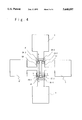
- FIG. 4 is a diagram showing of a test pattern used in a test method of measuring a contact resistance according to an embodiment of the present invention.
- the test pattern includes a contact hole section, and first to fourth electrode pad patterns 2, 4, 6, and 8 provided around the contact hole section such that they are connected to the contact hole section.
- the contact hole section includes first and second semiconductor region patterns 41 and 42 apart from each other and formed under an interlayer insulating film 20.
- First and second metal patterns 51 and 52 is provided above the first and second semiconductor region patterns 41 and 42 via an insulating film 20 apart from each other such that each of the first and second metal patterns 51 and 52 overlaps the first and second semiconductor region patterns 41 and 42.
- First and second contact holes 22-1 and 24-2 are provided in the overlapping portion to have a plug structure.
- the plug structure is filled with a conductive material.
- the first and second contact holes 22-1 and 24-2 are provided to connect between the first semiconductor region pattern 41 and the first and second metal patterns 51 and 52, respectively.
- the first and second contact holes 22-1 and 24-2 have first and second depths, respectively. In the embodiment, the first depth is twice more than the second depth.
- Third and fourth contact holes 22-2 and 24-1 having the plug structure are provided in the overlapping portion of the semiconductor region pattern 42 and the first and second metal patterns 51 and 52, and filled with the conductive material such that the contact holes 22-2 and 24-1 are provided to connect between the second semiconductor region pattern 42 and the first and second metal patterns 51 and 52.
- the third and fourth contact holes 22-1 and 24-1 have the second and first depths, respectively.
- Fifth and sixth contact holes 30-2 and 30-4 are provided to connect between the first and second semiconductor region patterns 41 and 42 and the first and second electrode pad patterns 2 and 4, respectively.
- the third and fourth electrode pad patterns 6 and 8 are symmetrically connected to the first and second metal patterns 51 and 52, respectively.
- the first and second metal patterns are desirably made of a same metal to have a same resistance and the first and second semiconductor region patterns desirably have a same impurity density.
- the first to fourth contact holes 22-1, 22-2, 24-1 and 24-2 have the same cross sectional area. In the embodiment, the contact holes 22-1 and 24-2 are provided with a distance less than 5 ⁇ m.
- FIGS. 5 and 6 show cross sectional views of the semiconductor device when it is cut along lines 5--5 and 6--6, respectively.
- the contact holes 22-1, 22-2 24-1 and 24-2 have the same diameter and the first depth of the contact holes 22-1 and 24-1 is twice more than the second depth of the contact holes 22-2 and 24-2.
- FIG. 7 is a diagram showing an equivalent circuit of the test pattern shown in FIG. 4. Any parasitic resistance is not taken into account. Referring to the FIG. 7, the equivalent circuit will be described below.
- a first terminal 12 and a second terminal 13 correspond to the electrode pads 6 and 8, respectively.
- a third terminal 14 and a fourth terminal 15 correspond to the electrode pads 2 and 4, respectively.
- plug resistances of the contact holes 22-1 and 22-2 are represented by
- ⁇ 1 and ⁇ 2 are resistivity of the conductive material filled in the contact holes 22-1 or 24-1 and 22-2 or 24-2, respectively, S 1 and S 2 are cross sectional area of the contact holes 22-1 or 24-1 and 22-2 or 24-2, and d 1 and d 2 are contact depth of the contact holes 22-1 or 24-1 and 22-2 or 24-2, are first depth and second depth in the embodiment.
- the plug resistance R P2 can be obtained using the voltage V, the currents I O , I B and I S as follows.
- the contact resistances R 1 and R 2 are measured and determined.
- the contact resistances R 1 and R 2 can be easily measured.
- a parasitic resistance such as a diffusion layer resistance and a wiring pattern resistance is not taken into account.
- the equivalent circuit is as shown in FIG. 8.
- r P2 r P3 because the test pattern is symmetric. Accordingly, the above equation (1) is satisfied. As a result, even if any parasitic resistance is present, it does not influence to the measuring result.
- the terminals 12 and 13 correspond to the electrode pads 2 and 4 and the terminals 14 and 15 correspond to the electrode pads 6 and 8.
- the currents I O , I S , and I B are measured in the same manner as described in the first embodiment. Therefore, the plug resistance and interfacial resistance can be separately determined.
- the electrode pads 6 and 8 are directly connected to the contact holes 22-1 and 22-2, and 24-1 and 24-2, i.e., the contact holes having the first depth and having the second depth.
- the electrode pad 2 is connected to the contact holes 22-1 and 24-2 via the contact hole 30-2 and the semiconductor region 41.
- the resistance of the metal wiring pattern, the contact resistance of the contact hole 30-2, and the resistance of the semiconductor region 41 function as a parasitic resistance which is connected to the contact holes 22-1 and 24-2 in series.
- the parasitic resistance is equivalently present between the terminals 14 and 15 when the currents I O , I S and I B . Therefore, the parasitic resistance cannot be cancelled, resulting in measuring error.
- the third embodiment since the electrode pads 6 and 8 are directly connected to the contact holes as described above, the parasitic resistance can be cancelled. Therefore, the lug resistance and interfacial resistance can be separately measured with higher precision than in the first embodiment.
- the contact holes 22-1 and 24-2 can be formed with a distance less than 5 ⁇ m. As a result, measuring error due to ununiformity on the wafer surface can be avoided. Further, the plug resistance and interfacial resistance can be separately measured with high precision without influence by any parasitic resistance.
- the method of separately measuring the plug resistance and interfacial resistance according to the fourth embodiment of the present invention will be described.
- an upper half of the test pattern shown in FIG. 4 is used as shown in FIG. 9.
- the measuring method is the same as the method shown in FIG. 2.
- the plug resistance can be directly measured without any error due to ununiformity on the wafer surface although the precision is lower than in the first to third embodiments because the bridge circuit is not used.
Landscapes
- Engineering & Computer Science (AREA)
- Manufacturing & Machinery (AREA)
- Computer Hardware Design (AREA)
- Microelectronics & Electronic Packaging (AREA)
- Physics & Mathematics (AREA)
- General Physics & Mathematics (AREA)
- Power Engineering (AREA)
- General Engineering & Computer Science (AREA)
- Automation & Control Theory (AREA)
- Testing Or Measuring Of Semiconductors Or The Like (AREA)
- Semiconductor Integrated Circuits (AREA)
- Measurement Of Resistance Or Impedance (AREA)
Abstract
A test pattern for contact resistance, includes a contact hole section, and first to fourth electrode pad patterns connected to the contact hole section. The contact hole section includes first and second semiconductor region patterns apart from each other, first and second metal patterns provided above the first and second semiconductor region patterns via an insulating film apart from each other such that each of the first and second metal patterns overlaps the first and second semiconductor region patterns, first and second contact holes each having a plug structure, filled with a conductive material, and respectively provided to connect between the first semiconductor region pattern and the first and second metal patterns, the first and second contact holes having first and second depths, respectively, third and fourth contact holes each having the plug structure, filled with the conductive material, and respectively provided to connect between the second semiconductor region pattern and the first and second metal patterns, the third and fourth contact holes having the second and first depths, respectively, and fifth and sixth contact holes provided to connect between the first and second semiconductor regions patterns and the first and second electrode pad patterns, respectively, wherein the third and fourth electrode pad patterns are connected to the first and second metal patterns, respectively.
Description
This is a divisional of application Ser. No. 08/541,160 filed on Oct. 11, 1995 pending.
1. Field of the Invention
The present invention relates to a test pattern for measuring an electric property in a semiconductor device and a test method using the test pattern, and more particularly, to a test pattern for measuring a contact resistance in a contact section and a test method using the test pattern.
2. Description of Related Art
Recently, the pattern size section in a semiconductor device becomes fine as progress of semiconductor technology. At the same time, the size of a contact hole also becomes fine. Further, an interlayer insulating film has been sufficiently planarized so that workability can be sufficiently accomplished. Conventionally, the interlayer insulating film had a hollow surface in a portion for a contact hole to have been formed. Accordingly, the depth of the contact hole was shallower by the hollow portion than the other portion of the interlayer insulating film. As described above, however, the planarization of surface is made to remove any hollow portion so that the depth of the contact hole becomes deep. As a result, since the plane size of the contact hole is also made fine, an aspect ratio of the contact hole increases abruptly. In the contact hole having such a great aspect ratio, there is typically employed a plug structure of contact in which electrically conductive material is filled in the contact hole in advance and which is covered by a metal layer, in order to prevent any break or disconnection between the conductive material and the metal layer. In this case, the contact resistance of the contact hole is composed of a plug resistance by the conductive material in the plug structure and an interfacial resistance between the conductive material and the metal layer.
When any failure is caused in the contact section, there is a case that it needs to be determined whether the cause is based on high plug resistance or high interfacial resistance. In this case, it is necessary to separately measure the plug resistance and the interfacial resistance. If the contact resistance is measured by use of a general method in the plug structure of contact, the sum of plug resistance and interfacial resistance, i.e., the contact resistance is measured. Thus, the plug resistance and interfacial resistance cannot be measured separately.
As a check pattern for separately measuring the plug resistance and the interfacial resistance is known a pattern disclosed in Japanese Laid Open Patent Disclosure (JP-A-Heisei5-129390). This check pattern is shown in FIG. 1. Referring to FIG. 1, the check pattern includes three electrode pad patterns 118, 119 and 120 formed on an interlayer insulating film. Four n-type semiconductor wiring patterns 117 and one n-type wiring pattern 115 which are formed under the interlayer insulating film are provided in series between the electrode pad patterns 118 and 119. Contact holes 116 are provided between the electrode pad pattern and the n-type wiring pattern and between the n-type wiring patterns such that the electrode pad patterns 118 and 119 are electrically connected. Similarly, four n-type semiconductor wiring patterns 114 and one n-type wiring pattern 115 which are formed under the interlayer insulating film are provided in series between the electrode pad patterns 119 and 120. The n-type wiring pattern 114 has the same width and depth as the wiring pattern 117 but the wiring pattern 114 is different from the wiring pattern 117 in length. Contact holes 116 all having the same size are provided between the electrode pad pattern and the n-type wiring patter and between the n-type wiring patterns such that the electrode pad patterns 119 and 120 are electrically connected.
In this check pattern, a first resistance and a second resistance are measured between the electrode pads 118 and 119 and between the electrode pads 119 and 120. As a result, a sheet resistance can be measured because the difference between the first and second resistances is based on the difference between the n-type semiconductor wiring patterns in length. Subsequently, using the resistance difference, the contact resistance can be determined precisely. In this conventional technique, however, the determined resistance is equal to the sum of the plug resistance and the interfacial resistance, i.e., the contact resistance in a case that the contact has the plug structure and the plug resistance and interfacial resistance cannot be separately measured.
For this reason, a test pattern shown in FIG. 2 is tried in order to separately measure a plug resistance and an interfacial resistance. Referring to FIG. 2, the check pattern includes three electrode pad patterns 218, 219 and 220 formed on an interlayer insulating film. Five n-type semiconductor wiring patterns 217 having the same size and same resistance which are formed under the interlayer insulating film 222 are provided in series between the electrode pad patterns 218 and 219. Contact holes 116 are provided between the electrode pad pattern 218 or 219 and the n-type wiring pattern 217 and between the n-type wiring patterns 217 such that the electrode pad patterns 118 and 119 are electrically connected. Similarly, five n-type semiconductor wiring patterns 217 which are formed under the interlayer insulating film 222 are provided in series between the electrode pad patterns 219 and 220. Contact holes 215 all having the same size are provided between the electrode pad pattern 219 or 220 and the n-type wiring pattern 217 and between the n-type wiring patterns 217 such that the electrode pad patterns 219 and 220 are electrically connected. In this case, the cross sectional views of the contact holes 216 and 215 when a semiconductor device is cut along lines 3A--3A and 3B--3B are shown in FIGS. 3A and 3B. As seen from the figures, the contact hole 216 has the same diameter as the contact hole 215 and the contact holes 216 and 215 are filled with the same conductive material. However, the contact hole 216 is different from the contact hole 215 in depth.
In this test pattern, a first resistance and a second resistance are measured between the electrode pads 218 and 219 and between the electrode pads 219 and 220. As a result, the difference of plug resistance between the contact holes 215 and 216 can be measured. Then, an interfacial resistance can be also determined using the determined plug resistance.
However, in the above conventional technique there is the following problem. That is, in order to make it possible to measure a resistance with probes, the dimension of test pattern is about 100×100 μm. As a result, the measuring result contains an error due to ununiformity on a wafer surface.
The present invention has, as an object, to provide a test pattern for separately measuring a plug resistance and interfacial resistance of a contact resistance.
Another object of the present invention is to provide a method of separately measuring a plug resistance and interfacial resistance of a contact resistance with high precision.
In order to achieve an aspect of the present invention, a test pattern for contact resistance, includes a contact hole section, and first to fourth electrode pad patterns connected to the contact hole section. The contact hole section includes first and second semiconductor region patterns apart from each other, first and second metal patterns provided above the first and second semiconductor region patterns via an insulating film apart from each other such that each of the first and second metal patterns overlaps the first and second semiconductor region patterns, first and second contact holes each having a plug structure, filled with a conductive material, and respectively provided to connect between the first semiconductor region pattern and the first and second metal patterns, the first and second contact holes having first and second depths, respectively, third and fourth contact holes each having the plug structure, filled with the conductive material, and respectively provided to connect between the second semiconductor region pattern and the first and second metal patterns, the third and fourth contact holes having the second and first depths, respectively, and fifth and sixth contact holes provided to connect between the first and second semiconductor regions patterns and the first and second electrode pad patterns, respectively, wherein the third and fourth electrode pad patterns are connected to the first and second metal patterns, respectively.
In this case, the first and second metal pattern is desirably made of a same metal to have a same resistance and the first and second semiconductor region patterns desirably have a same impurity density. Further, the first to fourth contact holes desirably have a same cross sectional area.
In order to achieve another aspect of the present invention, a method of determining a contact resistance composed of a plug resistance and an interfacial resistance, includes the steps of:
(a) providing on a semiconductor chip a test pattern as described above;
(b) applying a predetermined voltage between the electrode pad patterns of one of a pair of first and second electrode pad patterns and a pair of third and fourth electrode pad patterns and measuring a first current flowing between the electrode pad patterns of the one pair in an open state between the electrode pad patterns of the other pair;
(c) applying the predetermined voltage between the electrode pad patterns of the one pair and measuring a second current flowing between the electrode pad patterns of the one pair and a third current flowing between the electrode pad patterns of the other pair in a short state between the electrode pad patterns of the other pair;
(d) determining a first plug resistance of the first or fourth contact hole and a second plug resistance of the second or third contact hole from the voltage and the first to third currents.
The method may further includes the steps of:
(e) measuring a first contact resistance of the first or fourth contact hole and a second contact resistance of the second or third contact hole; and
(f) determining an interfacial resistance from a set of first contact resistance and first plug resistance or a set of second plug resistance and second contact resistance.
In this case, the first to fourth electrode pad patterns are desirably provided around the contact hole section. In measuring the currents, it is desirable that the one pair is of first and second electrode pads and the other pair is of third and fourth electrode pads. Alternatively, the one pair may be of third and fourth electrode pads and the other pair may be of first and second electrode pads.
In order to achieve another aspect of the present invention, a method of determining a contact resistance composed of a plug resistance and an interfacial resistance, includes the steps of:
(a) providing on a semiconductor chip a test pattern which comprises a contact hole section, and first to third electrode pad patterns provided around the contact hole section, wherein the contact hole section comprises:
a first semiconductor region pattern,
first and second metal patterns provided above the first semiconductor region pattern via an insulating film apart from each other to have a same resistance such that each of the first and second metal patterns overlaps the first semiconductor region pattern,
first and second contact holes each having a plug structure of a same diameter, filled with a conductive material, and respectively provided to connect between the first semiconductor region pattern and the first and second metal patterns, the first and second contact holes having first and second depths, respectively, and
a third contact hole provided to connect between the first semiconductor region pattern and the first electrode pad pattern, wherein the second and third electrode pad patterns are connected to the first and second metal patterns, respectively;
(b) applying a predetermined voltage between the first and second electrode pad patterns and measuring a first current flowing between the first and second electrode pad patterns;
(c) applying the predetermined voltage between the first and third electrode pad patterns and a second current flowing between the first and third electrode pad patterns;
(d) determining a first plug resistance of the first contact hole and a second plug resistance of the second contact hole from the voltage and the first and second currents.
The method may further includes the steps of:
(e) measuring a first contact resistance of the first contact hole and a second contact resistance of the second contact hole; and
(f) determining an interfacial resistance from a set of first contact resistance and first plug resistance or a set of second plug resistance and second contact resistance.
FIG. 1 is a conventional test pattern used for measuring a contact resistance;
FIG. 2 is another conventional test pattern used for measuring a plug resistance and an interfacial resistance of a contact resistance;
FIGS. 3A and 3B are cross sectional views when a semiconductor device is cut along an A-A' line and an B-B' line in FIG. 2, respectively;
FIG. 4 is a test pattern used for measuring a contact resistance including a plug resistance and an interfacial resistance according to an embodiment of the present invention;
FIG. 5 is a cross sectional view when a semiconductor device shown in FIG. 4 is cut along a V--V line;
FIG. 6 is a cross sectional view when a semiconductor device shown in FIG. 4 is cut along a VI--VI line;
FIG. 7 is an equivalent circuit of the test pattern shown in FIG. 4;
FIG. 8 is an equivalent circuit of the test pattern shown in FIG. 4 including a parasitic resistance; and
FIG. 9 is another test pattern used for measuring a contact resistance including a plug resistance and an interfacial resistance according to another embodiment of the present invention.
The present invention will be described below in detail with reference to the accompanying drawings.
FIG. 4 is a diagram showing of a test pattern used in a test method of measuring a contact resistance according to an embodiment of the present invention. Referring to FIG. 4, the test pattern includes a contact hole section, and first to fourth electrode pad patterns 2, 4, 6, and 8 provided around the contact hole section such that they are connected to the contact hole section. The contact hole section includes first and second semiconductor region patterns 41 and 42 apart from each other and formed under an interlayer insulating film 20. First and second metal patterns 51 and 52 is provided above the first and second semiconductor region patterns 41 and 42 via an insulating film 20 apart from each other such that each of the first and second metal patterns 51 and 52 overlaps the first and second semiconductor region patterns 41 and 42. First and second contact holes 22-1 and 24-2 are provided in the overlapping portion to have a plug structure. The plug structure is filled with a conductive material. The first and second contact holes 22-1 and 24-2 are provided to connect between the first semiconductor region pattern 41 and the first and second metal patterns 51 and 52, respectively. The first and second contact holes 22-1 and 24-2 have first and second depths, respectively. In the embodiment, the first depth is twice more than the second depth. Third and fourth contact holes 22-2 and 24-1 having the plug structure are provided in the overlapping portion of the semiconductor region pattern 42 and the first and second metal patterns 51 and 52, and filled with the conductive material such that the contact holes 22-2 and 24-1 are provided to connect between the second semiconductor region pattern 42 and the first and second metal patterns 51 and 52. The third and fourth contact holes 22-1 and 24-1 have the second and first depths, respectively. Fifth and sixth contact holes 30-2 and 30-4 are provided to connect between the first and second semiconductor region patterns 41 and 42 and the first and second electrode pad patterns 2 and 4, respectively. The third and fourth electrode pad patterns 6 and 8 are symmetrically connected to the first and second metal patterns 51 and 52, respectively. In this case, the first and second metal patterns are desirably made of a same metal to have a same resistance and the first and second semiconductor region patterns desirably have a same impurity density. The first to fourth contact holes 22-1, 22-2, 24-1 and 24-2 have the same cross sectional area. In the embodiment, the contact holes 22-1 and 24-2 are provided with a distance less than 5 μm.
FIGS. 5 and 6 show cross sectional views of the semiconductor device when it is cut along lines 5--5 and 6--6, respectively. As seen from the figures, the contact holes 22-1, 22-2 24-1 and 24-2 have the same diameter and the first depth of the contact holes 22-1 and 24-1 is twice more than the second depth of the contact holes 22-2 and 24-2.
FIG. 7 is a diagram showing an equivalent circuit of the test pattern shown in FIG. 4. Any parasitic resistance is not taken into account. Referring to the FIG. 7, the equivalent circuit will be described below. In FIG. 7, a sum of a plug resistance RP1 and interfacial resistance RC1 in the contact hole having the first depth (the contact hole 22-1 or 24-1 in FIG. 4) is represented by R1 (=RC1 +RP1). A sum of plug resistance RP2 and interfacial resistance RC2 in the contact hole having the second depth (the contact hole 22-2 or 24-2 in FIG. 4) is represented by R2 (=RC2 +RP2). A first terminal 12 and a second terminal 13 correspond to the electrode pads 6 and 8, respectively. A third terminal 14 and a fourth terminal 15 correspond to the electrode pads 2 and 4, respectively.
In FIG. 7, in an open state between the third and fourth terminals 14 and 15, a current IO flowing between the first and second terminals is first measured when a voltage V is applied between the first and second terminals 12 and 13. Subsequently, in a short state between the third and fourth terminals 14 and 15, a current IB flowing between the third and fourth terminals 14 and 15 and a current IS flowing between the first and second terminals 12 and 13 are measured when the voltage V is applied between the first and second terminals 12 and 13 in the same manner as described above. In this case, the following relation is obtained.
R.sub.1 -R.sub.2 =(2V/I.sub.B){1-(I.sub.S /I.sub.O)} (1)
In this embodiment, RC1 =RC2 is satisfied because the interfacial resistances are the same if the interfacial states are same. Accordingly, the following equation is satisfied.
R.sub.1 -R.sub.2 =(2V/I.sub.B){1-(I.sub.S /I.sub.O)}=R.sub.P1 -R.sub.P2(2)
Further, the plug resistances of the contact holes 22-1 and 22-2 are represented by
R.sub.P1 =ρ.sub.1 (d.sub.1 /S.sub.1), R.sub.P2 =ρ.sub.2 (d.sub.2 /S.sub.2)
where ρ1 and ρ2 are resistivity of the conductive material filled in the contact holes 22-1 or 24-1 and 22-2 or 24-2, respectively, S1 and S2 are cross sectional area of the contact holes 22-1 or 24-1 and 22-2 or 24-2, and d1 and d2 are contact depth of the contact holes 22-1 or 24-1 and 22-2 or 24-2, are first depth and second depth in the embodiment. In this embodiment, since ρ1 =ρ2 =ρ, S1 =S2 =S, and d1 =2d2, the following equation (3) can be obtained.
R.sub.P1 -R.sub.P2 =(ρ/S)(d.sub.1 -d.sub.2)=(ρ/S)(2d.sub.2 -d.sub.2)=(ρ/S)d.sub.2 =R.sub.P2 (3)
Therefore, the plug resistance RP2 can be obtained using the voltage V, the currents IO, IB and IS as follows.
R.sub.P2 =(2V/I.sub.B){1-(I.sub.S /I.sub.O)}
Next, the contact resistances R1 and R2 are measured and determined. The contact resistances R1 and R2 can be easily measured. In order to measure the contact resistances R1 and R2, the method shown in FIG. 1 may be used or another method may be used. If the contact resistances R1 and R2 are measured, the interfacial resistance RC1 (=RC2) can be determined from the following equations.
R.sub.C1 =R.sub.1 -R.sub.P1 =R.sub.1 -2R.sub.P2
R.sub.C2 =R.sub.2 -R.sub.P2
Next, the method of separately measuring the plug resistance and interfacial resistance according to the second embodiment of the present invention will be described.
In the above first embodiment, a parasitic resistance such as a diffusion layer resistance and a wiring pattern resistance is not taken into account. When such parasitic resistance is taken into account, the equivalent circuit is as shown in FIG. 8. In FIG. 8, resistors rPX (X=1 to 3) represent parasitic resistances. In this case, the following equation is established.
(R.sub.1 +r.sub.P2)-(R.sub.2 +r.sub.P3)=(2V/I.sub.B){1-(I.sub.S /I.sub.O)}
In the embodiment, rP2 =rP3 because the test pattern is symmetric. Accordingly, the above equation (1) is satisfied. As a result, even if any parasitic resistance is present, it does not influence to the measuring result.
Next, the method of separately measuring the plug resistance and interfacial resistance according to the third embodiment of the present invention will be described. In this embodiment, the terminals 12 and 13 correspond to the electrode pads 2 and 4 and the terminals 14 and 15 correspond to the electrode pads 6 and 8. The currents IO, IS, and IB are measured in the same manner as described in the first embodiment. Therefore, the plug resistance and interfacial resistance can be separately determined.
In the third embodiment, the electrode pads 6 and 8 are directly connected to the contact holes 22-1 and 22-2, and 24-1 and 24-2, i.e., the contact holes having the first depth and having the second depth. In the first embodiment, for instance, the electrode pad 2 is connected to the contact holes 22-1 and 24-2 via the contact hole 30-2 and the semiconductor region 41. The resistance of the metal wiring pattern, the contact resistance of the contact hole 30-2, and the resistance of the semiconductor region 41 function as a parasitic resistance which is connected to the contact holes 22-1 and 24-2 in series. The parasitic resistance is equivalently present between the terminals 14 and 15 when the currents IO, IS and IB. Therefore, the parasitic resistance cannot be cancelled, resulting in measuring error. On the other hand, the third embodiment, since the electrode pads 6 and 8 are directly connected to the contact holes as described above, the parasitic resistance can be cancelled. Therefore, the lug resistance and interfacial resistance can be separately measured with higher precision than in the first embodiment.
As described above, accordingly to the present invention, the contact holes 22-1 and 24-2 can be formed with a distance less than 5 μm. As a result, measuring error due to ununiformity on the wafer surface can be avoided. Further, the plug resistance and interfacial resistance can be separately measured with high precision without influence by any parasitic resistance.
Next, the method of separately measuring the plug resistance and interfacial resistance according to the fourth embodiment of the present invention will be described. In this embodiment, an upper half of the test pattern shown in FIG. 4 is used as shown in FIG. 9. The measuring method is the same as the method shown in FIG. 2. In this case, the plug resistance can be directly measured without any error due to ununiformity on the wafer surface although the precision is lower than in the first to third embodiments because the bridge circuit is not used.
Claims (6)
1. A test pattern for contact resistance, comprising:
a contact hole section; and
first to fourth electrode pad patterns provided around said contact hole section, and
wherein said contact hole section comprises:
first and second semiconductor region patterns apart from each other;
first and second metal patterns provided above said first and second semiconductor region patterns via an insulating film apart from each other such that each of said first and second metal patterns overlaps said first and second semiconductor region patterns;
first and second contact holes each having a plug structure, filled with a conductive material, and respectively provided to connect between said first semiconductor region pattern and said first and second metal patterns, said first and second contact holes having first and second depths, respectively;
third and fourth contact holes each having the plug structure, filled with the conductive material, and respectively provided to connect between said second semiconductor region pattern and said first and second metal patterns, said third and fourth contact holes having said second and first depths, respectively; and
fifth and sixth contact holes provided to connect between said first and second semiconductor regions patterns and said first and second electrode pad patterns, respectively, wherein said third and fourth electrode pad patterns are connected to said first and second metal patterns, respectively.
2. A test pattern according to claim 1, wherein said first and second metal pattern is made of a same metal to have a same resistance.
3. A test pattern according to claim 1, wherein said first to fourth contact holes have a same cross sectional area.
4. A test pattern according to claim 1, wherein said first and second semiconductor region patterns have a same impurity density.
5. A test pattern according to claim 1, wherein said first depth is twice more than said second depth.
6. A test pattern according to claim 1, wherein said third and fourth electrode pad patterns are symmetrically connected to said first and second metal patterns.
Priority Applications (1)
| Application Number | Priority Date | Filing Date | Title |
|---|---|---|---|
| US08/724,350 US5640097A (en) | 1994-10-19 | 1996-10-01 | Test pattern for separately determining plug resistance and interfactial resistance |
Applications Claiming Priority (4)
| Application Number | Priority Date | Filing Date | Title |
|---|---|---|---|
| JP6-279835 | 1994-10-19 | ||
| JP6279835A JP2718380B2 (en) | 1994-10-19 | 1994-10-19 | Semiconductor device electrical characteristics inspection pattern and inspection method |
| US08/541,160 US5663651A (en) | 1994-10-19 | 1995-10-11 | Method of separately determining plug resistor and interfacial resistor and test pattern for the same |
| US08/724,350 US5640097A (en) | 1994-10-19 | 1996-10-01 | Test pattern for separately determining plug resistance and interfactial resistance |
Related Parent Applications (1)
| Application Number | Title | Priority Date | Filing Date |
|---|---|---|---|
| US08/541,160 Division US5663651A (en) | 1994-10-19 | 1995-10-11 | Method of separately determining plug resistor and interfacial resistor and test pattern for the same |
Publications (1)
| Publication Number | Publication Date |
|---|---|
| US5640097A true US5640097A (en) | 1997-06-17 |
Family
ID=17616591
Family Applications (2)
| Application Number | Title | Priority Date | Filing Date |
|---|---|---|---|
| US08/541,160 Expired - Fee Related US5663651A (en) | 1994-10-19 | 1995-10-11 | Method of separately determining plug resistor and interfacial resistor and test pattern for the same |
| US08/724,350 Expired - Fee Related US5640097A (en) | 1994-10-19 | 1996-10-01 | Test pattern for separately determining plug resistance and interfactial resistance |
Family Applications Before (1)
| Application Number | Title | Priority Date | Filing Date |
|---|---|---|---|
| US08/541,160 Expired - Fee Related US5663651A (en) | 1994-10-19 | 1995-10-11 | Method of separately determining plug resistor and interfacial resistor and test pattern for the same |
Country Status (3)
| Country | Link |
|---|---|
| US (2) | US5663651A (en) |
| JP (1) | JP2718380B2 (en) |
| KR (1) | KR0180328B1 (en) |
Cited By (8)
| Publication number | Priority date | Publication date | Assignee | Title |
|---|---|---|---|---|
| FR2775832A1 (en) * | 1998-03-05 | 1999-09-10 | St Microelectronics Sa | Semiconductor substrate test circuit |
| US6525548B1 (en) * | 1999-11-12 | 2003-02-25 | Nec Corporation | Check pattern for a semiconductor device |
| US20030218168A1 (en) * | 2002-05-24 | 2003-11-27 | Takehiko Okajima | Semiconductor substrate and test pattern for the same |
| US20090065947A1 (en) * | 2007-09-11 | 2009-03-12 | Nec Electronics Corporation | Semiconductor device having circularly connected plural pads via through holes and method of evaluating the same |
| US20090066902A1 (en) * | 2000-10-17 | 2009-03-12 | Hong Jin Kim | Liquid crystal display for equivalent resistance wiring |
| CN102890195A (en) * | 2011-07-20 | 2013-01-23 | 上海华虹Nec电子有限公司 | Structure and method for testing resistances of contact holes on same type active region with substrate |
| US20140327459A1 (en) * | 2013-05-06 | 2014-11-06 | Samsung Display Co., Ltd. | Substrate of electronic device, electronic device including the same, and measuring method of resistance at connection portion |
| US20160133586A1 (en) * | 2014-11-11 | 2016-05-12 | Samsung Electronics Co., Ltd. | Semiconductor device |
Families Citing this family (6)
| Publication number | Priority date | Publication date | Assignee | Title |
|---|---|---|---|---|
| US6323661B1 (en) * | 1999-05-03 | 2001-11-27 | General Electric Company | Measurement of printed circuit-to-conductive substrate contact resistance |
| KR100336792B1 (en) * | 2000-05-25 | 2002-05-16 | 박종섭 | Test pattern for evaluating a process of silicide film fabrication |
| KR100403319B1 (en) * | 2001-12-20 | 2003-10-30 | 주식회사 하이닉스반도체 | Method for forming a test pattern of semiconductor device |
| KR100555504B1 (en) * | 2003-06-27 | 2006-03-03 | 삼성전자주식회사 | Test structure for detecting a defect size in a semiconductor device and test method using the same |
| CN101764124B (en) * | 2008-12-25 | 2011-10-26 | 上海北京大学微电子研究院 | Measurement structure of interconnection resistance and method thereof |
| KR102085973B1 (en) * | 2013-06-18 | 2020-03-06 | 에스케이하이닉스 주식회사 | Test circuit of semiconductor device and test method of semiconductor device |
Citations (3)
| Publication number | Priority date | Publication date | Assignee | Title |
|---|---|---|---|---|
| JPS6333665A (en) * | 1986-07-28 | 1988-02-13 | Matsushita Electric Ind Co Ltd | Contact resistance measuring pattern |
| JPH05129390A (en) * | 1991-10-31 | 1993-05-25 | Nec Kyushu Ltd | Pattern for checking electrical characteristics of semiconductor device |
| US5450016A (en) * | 1993-06-30 | 1995-09-12 | Nec Corporation | Method of quickly evaluating contact resistance of semiconductor device |
Family Cites Families (5)
| Publication number | Priority date | Publication date | Assignee | Title |
|---|---|---|---|---|
| JPH0482248A (en) * | 1990-07-25 | 1992-03-16 | Sumitomo Electric Ind Ltd | Evaluation method of semiconductor device |
| JPH0541440A (en) * | 1991-02-08 | 1993-02-19 | Toshiba Corp | Measuring method for contact area of contact hole |
| JPH04324951A (en) * | 1991-04-25 | 1992-11-13 | Nec Corp | Semiconductor device |
| JP2665075B2 (en) * | 1991-06-06 | 1997-10-22 | 日本電気アイシーマイコンシステム株式会社 | Integrated circuit check pattern and check method thereof |
| JPH053237A (en) * | 1991-06-25 | 1993-01-08 | Oki Electric Ind Co Ltd | Method of detecting misalignment between through-hole and upper layer wiring |
-
1994
- 1994-10-19 JP JP6279835A patent/JP2718380B2/en not_active Expired - Fee Related
-
1995
- 1995-10-11 US US08/541,160 patent/US5663651A/en not_active Expired - Fee Related
- 1995-10-17 KR KR1019950035841A patent/KR0180328B1/en not_active IP Right Cessation
-
1996
- 1996-10-01 US US08/724,350 patent/US5640097A/en not_active Expired - Fee Related
Patent Citations (3)
| Publication number | Priority date | Publication date | Assignee | Title |
|---|---|---|---|---|
| JPS6333665A (en) * | 1986-07-28 | 1988-02-13 | Matsushita Electric Ind Co Ltd | Contact resistance measuring pattern |
| JPH05129390A (en) * | 1991-10-31 | 1993-05-25 | Nec Kyushu Ltd | Pattern for checking electrical characteristics of semiconductor device |
| US5450016A (en) * | 1993-06-30 | 1995-09-12 | Nec Corporation | Method of quickly evaluating contact resistance of semiconductor device |
Cited By (17)
| Publication number | Priority date | Publication date | Assignee | Title |
|---|---|---|---|---|
| US6166607A (en) * | 1998-03-05 | 2000-12-26 | Stmicroelectronics S.A. | Semiconductor test structure formed in cutting path of semiconductor water |
| FR2775832A1 (en) * | 1998-03-05 | 1999-09-10 | St Microelectronics Sa | Semiconductor substrate test circuit |
| US6525548B1 (en) * | 1999-11-12 | 2003-02-25 | Nec Corporation | Check pattern for a semiconductor device |
| US20090066902A1 (en) * | 2000-10-17 | 2009-03-12 | Hong Jin Kim | Liquid crystal display for equivalent resistance wiring |
| US7911575B2 (en) | 2000-10-17 | 2011-03-22 | Lg Display Co., Ltd. | Liquid crystal display for compensating resistance differences of electrode link |
| US7626673B2 (en) * | 2000-10-17 | 2009-12-01 | Lg Display Co., Ltd. | Liquid crystal display for equivalent resistance wiring |
| US20050051902A1 (en) * | 2002-05-24 | 2005-03-10 | Takehiko Okajima | Semiconductor substrate and test pattern for the same |
| US7078920B2 (en) * | 2002-05-24 | 2006-07-18 | Oki Electric Industry Co., Ltd. | Semiconductor substrate and test pattern for the same |
| US7053634B2 (en) * | 2002-05-24 | 2006-05-30 | Oki Electric Industry Co., Ltd. | Test pattern for testing contact resistance of a subject via hole |
| US20030218168A1 (en) * | 2002-05-24 | 2003-11-27 | Takehiko Okajima | Semiconductor substrate and test pattern for the same |
| US20090065947A1 (en) * | 2007-09-11 | 2009-03-12 | Nec Electronics Corporation | Semiconductor device having circularly connected plural pads via through holes and method of evaluating the same |
| CN102890195A (en) * | 2011-07-20 | 2013-01-23 | 上海华虹Nec电子有限公司 | Structure and method for testing resistances of contact holes on same type active region with substrate |
| CN102890195B (en) * | 2011-07-20 | 2015-02-04 | 上海华虹宏力半导体制造有限公司 | Method for testing resistances of contact holes on same type active region with substrate |
| US20140327459A1 (en) * | 2013-05-06 | 2014-11-06 | Samsung Display Co., Ltd. | Substrate of electronic device, electronic device including the same, and measuring method of resistance at connection portion |
| US9299280B2 (en) * | 2013-05-06 | 2016-03-29 | Samsung Display Co., Ltd. | Substrate of electronic device, electronic device including the same, and measuring method of resistance at connection portion |
| US20160133586A1 (en) * | 2014-11-11 | 2016-05-12 | Samsung Electronics Co., Ltd. | Semiconductor device |
| US9911706B2 (en) * | 2014-11-11 | 2018-03-06 | Samsung Electronics Co., Ltd. | Semiconductor device |
Also Published As
| Publication number | Publication date |
|---|---|
| US5663651A (en) | 1997-09-02 |
| KR960015835A (en) | 1996-05-22 |
| JPH08124987A (en) | 1996-05-17 |
| KR0180328B1 (en) | 1999-04-15 |
| JP2718380B2 (en) | 1998-02-25 |
Similar Documents
| Publication | Publication Date | Title |
|---|---|---|
| US5640097A (en) | Test pattern for separately determining plug resistance and interfactial resistance | |
| US5196373A (en) | Method of making trench conductor and crossunder architecture | |
| US6272736B1 (en) | Method for forming a thin-film resistor | |
| US6690187B2 (en) | Apparatus for testing reliability of interconnection in integrated circuit | |
| JPH0418471B2 (en) | ||
| US5119168A (en) | Semiconductor integrated circuit | |
| US6080597A (en) | Test pattern structure for measuring misalignment in semiconductor device fabrication process and method for measuring misalignment | |
| KR100267108B1 (en) | Semiconductor device having multi-layer metal interconnection and method fabricating the same | |
| US5543633A (en) | Process and structure for measuring the planarity degree of a dielectric layer in an integrated circuit and integrated circuit including means for performing said process | |
| KR100414223B1 (en) | Apparatus for testing reliability of metal line in integrated circuit | |
| US6597277B2 (en) | Termination resistor in printed circuit board | |
| US6013952A (en) | Structure and method for measuring interface resistance in multiple interface contacts and via structures in semiconductor devices | |
| KR20000026196A (en) | Test structure for measuring minimum area design and method therefor | |
| US20030186470A1 (en) | Structure and method for determining edges of regions in a semiconductor wafer | |
| JP2825046B2 (en) | Characteristics measuring element | |
| KR20020017746A (en) | A method for forming a test pattern of a semiconductor device | |
| JPS6127691A (en) | Internal wiring structure of magnetoresistance element | |
| JPH0541440A (en) | Measuring method for contact area of contact hole | |
| JPH0766263A (en) | Contact resistance measuring method of multilayered metal wiring, semiconductor device and wafer | |
| JP3223961B2 (en) | Interlayer film flatness measuring function element and interlayer film flatness evaluation method | |
| JP2891729B2 (en) | Measuring method of dielectric isolation substrate and its measuring device | |
| KR19990025636A (en) | Method for measuring via contact hole resistance of semiconductor device | |
| US6525417B2 (en) | Integrated circuits having reduced step height by using dummy conductive lines | |
| JPH01319956A (en) | Semiconductor integrated circuit | |
| KR19990066372A (en) | Semiconductor test pattern |
Legal Events
| Date | Code | Title | Description |
|---|---|---|---|
| FPAY | Fee payment |
Year of fee payment: 4 |
|
| FPAY | Fee payment |
Year of fee payment: 8 |
|
| REMI | Maintenance fee reminder mailed | ||
| LAPS | Lapse for failure to pay maintenance fees | ||
| STCH | Information on status: patent discontinuation |
Free format text: PATENT EXPIRED DUE TO NONPAYMENT OF MAINTENANCE FEES UNDER 37 CFR 1.362 |
|
| FP | Lapsed due to failure to pay maintenance fee |
Effective date: 20090617 |