US5410804A - Method for manufacturing a single product from integrated circuits received on a lead frame - Google Patents
Method for manufacturing a single product from integrated circuits received on a lead frame Download PDFInfo
- Publication number
- US5410804A US5410804A US08/117,154 US11715493A US5410804A US 5410804 A US5410804 A US 5410804A US 11715493 A US11715493 A US 11715493A US 5410804 A US5410804 A US 5410804A
- Authority
- US
- United States
- Prior art keywords
- leads
- integrated circuit
- cutting
- lead
- lead frame
- Prior art date
- Legal status (The legal status is an assumption and is not a legal conclusion. Google has not performed a legal analysis and makes no representation as to the accuracy of the status listed.)
- Expired - Fee Related
Links
- 238000000034 method Methods 0.000 title claims abstract description 17
- 238000004519 manufacturing process Methods 0.000 title claims abstract description 7
- 238000005520 cutting process Methods 0.000 claims abstract description 18
- 238000005452 bending Methods 0.000 claims abstract description 8
- 238000003754 machining Methods 0.000 claims description 23
- 238000006073 displacement reaction Methods 0.000 claims description 3
- 230000006978 adaptation Effects 0.000 description 1
- 230000007306 turnover Effects 0.000 description 1
Images


Classifications
-
- H—ELECTRICITY
- H01—ELECTRIC ELEMENTS
- H01L—SEMICONDUCTOR DEVICES NOT COVERED BY CLASS H10
- H01L21/00—Processes or apparatus adapted for the manufacture or treatment of semiconductor or solid state devices or of parts thereof
- H01L21/02—Manufacture or treatment of semiconductor devices or of parts thereof
- H01L21/04—Manufacture or treatment of semiconductor devices or of parts thereof the devices having at least one potential-jump barrier or surface barrier, e.g. PN junction, depletion layer or carrier concentration layer
- H01L21/48—Manufacture or treatment of parts, e.g. containers, prior to assembly of the devices, using processes not provided for in a single one of the subgroups H01L21/06 - H01L21/326
- H01L21/4814—Conductive parts
- H01L21/4821—Flat leads, e.g. lead frames with or without insulating supports
- H01L21/4842—Mechanical treatment, e.g. punching, cutting, deforming, cold welding
-
- Y—GENERAL TAGGING OF NEW TECHNOLOGICAL DEVELOPMENTS; GENERAL TAGGING OF CROSS-SECTIONAL TECHNOLOGIES SPANNING OVER SEVERAL SECTIONS OF THE IPC; TECHNICAL SUBJECTS COVERED BY FORMER USPC CROSS-REFERENCE ART COLLECTIONS [XRACs] AND DIGESTS
- Y10—TECHNICAL SUBJECTS COVERED BY FORMER USPC
- Y10T—TECHNICAL SUBJECTS COVERED BY FORMER US CLASSIFICATION
- Y10T29/00—Metal working
- Y10T29/49—Method of mechanical manufacture
- Y10T29/49002—Electrical device making
- Y10T29/49117—Conductor or circuit manufacturing
- Y10T29/49121—Beam lead frame or beam lead device
-
- Y—GENERAL TAGGING OF NEW TECHNOLOGICAL DEVELOPMENTS; GENERAL TAGGING OF CROSS-SECTIONAL TECHNOLOGIES SPANNING OVER SEVERAL SECTIONS OF THE IPC; TECHNICAL SUBJECTS COVERED BY FORMER USPC CROSS-REFERENCE ART COLLECTIONS [XRACs] AND DIGESTS
- Y10—TECHNICAL SUBJECTS COVERED BY FORMER USPC
- Y10T—TECHNICAL SUBJECTS COVERED BY FORMER US CLASSIFICATION
- Y10T29/00—Metal working
- Y10T29/53—Means to assemble or disassemble
- Y10T29/5313—Means to assemble electrical device
Definitions
- the invention relates to a method and device for manufacturing a single product from integrated circuits received on a lead frame.
- products Up to the present time such products have usually been obtained using fully automatic or semi-automatic devices by cutting away from each product the strips connecting the leads, the so-called dam bars, subsequently bending and cutting to length the connecting strips (leads) and finally separating the individual products from the lead frames. All operations performed on the products are therefore carried out while the products are received in the lead frame. This enables operations to be carried out on groups of leads and to therefore increase the production speed. All of this is only possible however if the lead frames with the integrated, encapsulated circuits thereon are manufactured with very fine tolerances. Such a method is disclosed in EP-A-0 330 512.
- 4,103,718 discloses a device for cutting away dam bars of a lead frame.
- This production method is not suitable for products such as pilot series of for instance 10-1000 products, for example on laboratory scale.
- the variations in dimensions can be relatively large, for instance because, as a result of tests with other encapsulating material, the shrink of the lead frames differs to that in the case of use of another encapsulating material.
- the devices developed for large-scale use cannot be employed because they are too expensive.
- Up to the present time pilot series and the like have in practice often be manufactured by hand. This involves much time and manpower.
- the invention has for its object to provide a method and means enabling processing of a great variety of products at comparatively low price.
- the dam bars are preferably cut through one by one.
- the leads on one side of a product are bent round in groups.
- a device is further provided according to the invention with which it is possible, as a result only of changing a tool, to cut products out of the lead frame, bend the leads and cut the leads to length.
- the device further enables adjusting of the tool within a relatively wide range relative to the product so that adaptation to the dimensions of each product, the desired lead length and the like is possible.
- a device for performing method step b of the method as according to claim 1 is characterized by a table transportable through a lead pitch, a carriage placed on the table for receiving and clamping a product and a machining member vertically movable relative to the carriage.
- the table is further displaceable in a direction perpendicular to the pitch displacement.
- a cutting member is chosen as machining member.
- the machining member is preferably received in a tool holder which is displaceable relative to the member vertically driving the tool holder as desired between an active position and a position located vertically at a higher point relative to the active position.
- the displacing of the tool holder takes place using a wedge-shaped control element movable transversely of the tool holder.
- the movement of the control element is bounded by a stop placeable in the path of movement.
- the driving of the table in the pitch direction takes place using a stepping motor.
- a device for performing the method steps a, c and d as according to claim 1, which is characterized by a frame, a table, clamping means on the table for clampingly receiving a product and a machining member movable vertically with respect to the table.
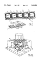
- FIGS. 1-4 show schematically the different method steps
- FIGS. 1A-5A show details of the method steps according to FIG. 1-4.
- a lead frame 1 comprises a number of mutually connected, encapsulated integrated circuits 2, 3, 4, 5, 6, subsequently referred to as products. According to the invention the products are first separated from the lead frame by cutting through the connection on the boundary line 7 between the products (FIG. 1).
- a cut-off product is subsequently machined in a machining device 8.
- the dam bars 9 are first cut through one by one (FIG. 2).
- the connecting strips (leads) 10 are bent in groups (FIG. 3) and finally the leads are cut to length (FIG. 4).
- the machining device according to FIG. 2 is shown perspectively in more detail in FIG. 2A.
- the machining device 8 is built up of a frame 11 in which guides 12, 14 for a table 13 are received.
- the table 13 is driven by a stepping motor 15 via a screw spindle 30.
- carriages 16 Placed on the table 13 are carriages 16, the first of which is displaceable over a guide 17.
- the carriages 16 comprise means for receiving and clamping a product that has to be machined.
- the first carriage 16 is adjustable manually by means of an adjusting member 18.
- a second carriage 16 is displaceable and adjustable in a direction at approximately 45° to the guide 17 using the slot-eccentric connection 19.
- a tool holder 20 which is vertically driven by drive means (not drawn). During the vertical stroke the machining member 21 coupled to the tool holder 20 performs a machining on the product 22 clamped onto the carriage 16.
- the tool holder 20 is displaceable in its guiding between an active position and a position releasing the product 22.
- a manually operable control element 23 is received slidably in lengthwise direction in a slot 24.
- the control element 23 has a sloping portion 25 which lies against a correspondingly inclining portion 26 of the tool holder 20.
- control element 23 The different positions of the control element 23 are fixed by a stop pin 31 which protrudes into a keysway 32.
- the device according to the invention it is possible to perform all desired operations on a product of which the dimensions lie within wide tolerance limits. Due to the many adjustment options the position on the table with respect to the machining member can be selected subject to the product. When the desired position of the product with respect to the machining member has been assumed the machining can take place, wherein the table with the product can be moved by the stepping motor over the length of a lead pitch.
- FIG. 5A which shows a variant of the embodiment according to FIG. 2A
- the adjusting means 17, 18 are replaced by adjusting blocks 33 which are arranged displaceably on the table.
- FIGS. 1A, 3A and 4A show in principle the same auxiliary device consisting of a frame 40, a table 41, clamping means 42 and a machining member 43 movable vertically with respect to the table 41.
- the product is clamped onto the table and, depending on the operation to be performed, a bending or cutting member is chosen as machining member.
Abstract
Encapsulated integrated circuits (chips) (2, 3, 4, 5, 6) are manufactured by separating the encapsulated integrated circuits arranged on a lead frame (1), subsequently cutting away the lead-connecting strips (7) of the individual products, then bending the leads and finally cutting them to length. By subjecting the products individually to the above stated method steps, products in a great variety of dimensions can be processed. The method and device according to the invention are particularly suitable for manufacturing pilot series on laboratory scale.
Description
The invention relates to a method and device for manufacturing a single product from integrated circuits received on a lead frame. Up to the present time such products have usually been obtained using fully automatic or semi-automatic devices by cutting away from each product the strips connecting the leads, the so-called dam bars, subsequently bending and cutting to length the connecting strips (leads) and finally separating the individual products from the lead frames. All operations performed on the products are therefore carried out while the products are received in the lead frame. This enables operations to be carried out on groups of leads and to therefore increase the production speed. All of this is only possible however if the lead frames with the integrated, encapsulated circuits thereon are manufactured with very fine tolerances. Such a method is disclosed in EP-A-0 330 512. U.S. Pat. No. 4,103,718 discloses a device for cutting away dam bars of a lead frame. This production method is not suitable for products such as pilot series of for instance 10-1000 products, for example on laboratory scale. The variations in dimensions can be relatively large, for instance because, as a result of tests with other encapsulating material, the shrink of the lead frames differs to that in the case of use of another encapsulating material. In such conditions the devices developed for large-scale use cannot be employed because they are too expensive. Up to the present time pilot series and the like have in practice often be manufactured by hand. This involves much time and manpower.
The invention has for its object to provide a method and means enabling processing of a great variety of products at comparatively low price.
This is achieved according to the invention by applying a method for successively performing on individual products arranged on a support frame with leads and consisting of encapsulated, integrated circuits the following method steps of:
a. cutting individual products out of the lead frame,
b. cutting away lead-connecting strips (dam bars),
c. bending the leads, and
d. cutting the leads to the desired length.
Because the individual product is first separated from the lead frame sufficient "space" is created round the product for it to undergo the subsequent operations. That is, means can be used which are allowed sufficient displacement space at the sides of the product without being obstructed by another product received in a lead frame and located adjacent to the product for machining.
The dam bars are preferably cut through one by one. The leads on one side of a product are bent round in groups.
A device is further provided according to the invention with which it is possible, as a result only of changing a tool, to cut products out of the lead frame, bend the leads and cut the leads to length.
The device further enables adjusting of the tool within a relatively wide range relative to the product so that adaptation to the dimensions of each product, the desired lead length and the like is possible.
A device for performing method step b of the method as according to claim 1 is characterized by a table transportable through a lead pitch, a carriage placed on the table for receiving and clamping a product and a machining member vertically movable relative to the carriage.
The table is further displaceable in a direction perpendicular to the pitch displacement. A cutting member is chosen as machining member.
In order after a machining to obtain sufficient free height for manually displacing or exchanging a product, the machining member is preferably received in a tool holder which is displaceable relative to the member vertically driving the tool holder as desired between an active position and a position located vertically at a higher point relative to the active position.
The displacing of the tool holder takes place using a wedge-shaped control element movable transversely of the tool holder.
The movement of the control element is bounded by a stop placeable in the path of movement.
The driving of the table in the pitch direction takes place using a stepping motor.
A device is further provided according to the invention for performing the method steps a, c and d as according to claim 1, which is characterized by a frame, a table, clamping means on the table for clampingly receiving a product and a machining member movable vertically with respect to the table.
The invention will be elucidated with reference to the drawings of an embodiment.
In the drawings:
FIGS. 1-4 show schematically the different method steps, and
FIGS. 1A-5A show details of the method steps according to FIG. 1-4.
A lead frame 1 comprises a number of mutually connected, encapsulated integrated circuits 2, 3, 4, 5, 6, subsequently referred to as products. According to the invention the products are first separated from the lead frame by cutting through the connection on the boundary line 7 between the products (FIG. 1).
A cut-off product is subsequently machined in a machining device 8. The dam bars 9 are first cut through one by one (FIG. 2). Thereafter the connecting strips (leads) 10 are bent in groups (FIG. 3) and finally the leads are cut to length (FIG. 4).
The machining device according to FIG. 2 is shown perspectively in more detail in FIG. 2A.
The machining device 8 is built up of a frame 11 in which guides 12, 14 for a table 13 are received. The table 13 is driven by a stepping motor 15 via a screw spindle 30. Placed on the table 13 are carriages 16, the first of which is displaceable over a guide 17. The carriages 16 comprise means for receiving and clamping a product that has to be machined. The first carriage 16 is adjustable manually by means of an adjusting member 18. In addition a second carriage 16 is displaceable and adjustable in a direction at approximately 45° to the guide 17 using the slot-eccentric connection 19.
Further connected to the frame is a tool holder 20 which is vertically driven by drive means (not drawn). During the vertical stroke the machining member 21 coupled to the tool holder 20 performs a machining on the product 22 clamped onto the carriage 16.
The tool holder 20 is displaceable in its guiding between an active position and a position releasing the product 22. For this purpose a manually operable control element 23 is received slidably in lengthwise direction in a slot 24. The control element 23 has a sloping portion 25 which lies against a correspondingly inclining portion 26 of the tool holder 20. When the control knob 27 is pulled in the direction of the arrow the control element 23 slides outward and the tool holder 20 moves in upward direction under the influence of the force exerted by the spring 28 on the portion 29 of the tool holder 20. Sufficient space is thereby created under the machining member to pick up, turn over or exchange the product 22 by hand.
When the control element 23 is shifted wholly outward the tool holder moves so far in upward direction that the machining member 21 can be exchanged.
The different positions of the control element 23 are fixed by a stop pin 31 which protrudes into a keysway 32.
Using the device according to the invention it is possible to perform all desired operations on a product of which the dimensions lie within wide tolerance limits. Due to the many adjustment options the position on the table with respect to the machining member can be selected subject to the product. When the desired position of the product with respect to the machining member has been assumed the machining can take place, wherein the table with the product can be moved by the stepping motor over the length of a lead pitch.
According to FIG. 5A, which shows a variant of the embodiment according to FIG. 2A, the adjusting means 17, 18 are replaced by adjusting blocks 33 which are arranged displaceably on the table.
FIGS. 1A, 3A and 4A show in principle the same auxiliary device consisting of a frame 40, a table 41, clamping means 42 and a machining member 43 movable vertically with respect to the table 41.
The product is clamped onto the table and, depending on the operation to be performed, a bending or cutting member is chosen as machining member.
Claims (9)
1. A method for manufacturing an individual product from an encapsulated, integrated circuit arranged on a support frame with leads, comprising the consecutive steps of:
a. cutting the individual encapsulated, integrated circuit out of a lead frame;
b. cutting away lead-connecting strips to form leads;
c. bending the leads; and
d. cutting the leads to a desired length.
2. The method of claim 1, wherein the lead-connecting strips are cut away one by one.
3. The method of claim 1, wherein the step of bending the leads comprises bending one group of leads at a time located on one side of the encapsulated, integrated circuit.
4. A device for cutting away strips between leads on an individual encapsulated, integrated circuit arranged on a support frame, comprising:
a table transportable over one lead pitch and in a direction perpendicular to a pitch displacement of the leads;
a carriage placed on the table for receiving and clamping an encapsulated integrated circuit; and
a machining member vertically movable relative to the carriage, wherein the machining member is used to cut the strips between the leads.
5. The device of claim 4, further comprising:
a tool holder for receiving the machining member so as to be vertically driven by the machining member, the tool holder being displaceable vertically relative to the machining member between an active position and a position located vertically at a higher point relative to the active position.
6. The device of claim 5, wherein the tool holder is displaced using a wedge-shaped control element movable transversely of the tool holder.
7. The device of claim 6, wherein the movement of the control element is bounded by a stop placeable in the path of movement.
8. The device of claim 4, wherein the table is driven in a pitch direction by a stepping motor.
9. A method for manufacturing a single product from an integrated circuit mounted on a lead frame, comprising the consecutive steps of:
cutting an individual integrated circuit out of a lead frame;
cutting away a lead-connecting strip which connects the leads of the lead frame, thereby forming a plurality of leads;
bending the leads; and
cutting the leads to a desired length.
Applications Claiming Priority (2)
| Application Number | Priority Date | Filing Date | Title |
|---|---|---|---|
| NL9100470A NL9100470A (en) | 1991-03-15 | 1991-03-15 | METHOD AND APPARATUS FOR MANUFACTURING A SINGLE PRODUCT FROM INTEGRATED CIRCUITS INCLUDED ON A LEADFRAME |
| NL9100470 | 1991-03-15 |
Publications (1)
| Publication Number | Publication Date |
|---|---|
| US5410804A true US5410804A (en) | 1995-05-02 |
Family
ID=19859026
Family Applications (1)
| Application Number | Title | Priority Date | Filing Date |
|---|---|---|---|
| US08/117,154 Expired - Fee Related US5410804A (en) | 1991-03-15 | 1993-09-14 | Method for manufacturing a single product from integrated circuits received on a lead frame |
Country Status (6)
| Country | Link |
|---|---|
| US (1) | US5410804A (en) |
| EP (1) | EP0575398A1 (en) |
| JP (1) | JPH06505831A (en) |
| MY (1) | MY108646A (en) |
| NL (1) | NL9100470A (en) |
| WO (1) | WO1992016968A1 (en) |
Cited By (8)
| Publication number | Priority date | Publication date | Assignee | Title |
|---|---|---|---|---|
| US5661090A (en) * | 1995-06-30 | 1997-08-26 | Sumitomo Metal (Smi) Electronics Devices, Inc. | Process and apparatus for manufacturing ceramic semiconductor packages |
| US5789280A (en) * | 1994-10-11 | 1998-08-04 | Motorola, Inc. | Leadframe having secured outer leads, semiconductor device using the leadframe and method of making them |
| US6085411A (en) * | 1996-12-09 | 2000-07-11 | International Business Machines Corporation | Fixture for making laminated integrated circuit devices |
| US20090093086A1 (en) * | 2007-10-03 | 2009-04-09 | Nec Electronics Corporation | Lead forming apparatus and method of fabricating semiconductor device |
| US9190351B2 (en) * | 2014-01-17 | 2015-11-17 | Freescale Semiconductor, Inc. Austin | Semiconductor device with webbing between leads |
| US10647016B2 (en) | 2017-11-06 | 2020-05-12 | Fancort Industries, Inc. | Interchangeable spring pack for an upper die in a lead forming system |
| CN114589252A (en) * | 2022-03-15 | 2022-06-07 | 铜陵华锐科技有限公司 | Shearing mechanism is used in lead frame production |
| CN115041580A (en) * | 2022-08-16 | 2022-09-13 | 华羿微电子股份有限公司 | Single separation device of lead frame |
Families Citing this family (1)
| Publication number | Priority date | Publication date | Assignee | Title |
|---|---|---|---|---|
| US5778947A (en) * | 1997-05-09 | 1998-07-14 | United Technologies Corporated | Bent lead repair tool for electronic components |
Citations (13)
| Publication number | Priority date | Publication date | Assignee | Title |
|---|---|---|---|---|
| US3650232A (en) * | 1970-09-08 | 1972-03-21 | Amp Inc | Method and apparatus for manufacturing lead frames |
| US4103718A (en) * | 1977-10-06 | 1978-08-01 | Honeywell Information Systems Inc. | Apparatus for cutting and forming flexible beam leads of an integrated circuit chip |
| FR2498377A1 (en) * | 1981-01-16 | 1982-07-23 | Thomson Csf Mat Tel | Semiconductor components mfr. on metal band - allows more connecting conductors by not connecting them to heat dissipator formed from metal band |
| JPS58151047A (en) * | 1982-03-03 | 1983-09-08 | Nippon Mining Co Ltd | Lead frame tape cutting apparatus |
| JPS6194349A (en) * | 1984-10-16 | 1986-05-13 | Sanken Electric Co Ltd | Manufacture of resin seal type semiconductor device and lead frame used for said manufacture |
| EP0330512A2 (en) * | 1988-02-24 | 1989-08-30 | Fujitsu Limited | Producing electronic components with the aid of lead frames |
| US4907628A (en) * | 1988-10-28 | 1990-03-13 | Fancort Industries, Inc. | Process and device for forming leads |
| US5012664A (en) * | 1988-12-12 | 1991-05-07 | Micron Technology, Inc. | Progressive form die |
| US5078186A (en) * | 1989-09-28 | 1992-01-07 | Kabushiki Kaisha Toshiba | Lead forming for electronic parts having gull wing type outer leads |
| US5127447A (en) * | 1990-04-25 | 1992-07-07 | Kabushiki Kaisha Toshiba | Method of bending outer leads of a semiconductor device |
| US5146662A (en) * | 1991-12-30 | 1992-09-15 | Fierkens Richard H J | Lead frame cutting apparatus for various sized integrated circuit packages and method therefor |
| US5251679A (en) * | 1991-06-26 | 1993-10-12 | Siemens Nixdorf Informationssysteme Ag | Apparatus for shaping outboard terminals of surface-mountable circuit modules |
| US5271148A (en) * | 1988-11-17 | 1993-12-21 | National Semiconductor Corporation | Method of producing a leadframe |
-
1991
- 1991-03-15 NL NL9100470A patent/NL9100470A/en not_active Application Discontinuation
-
1992
- 1992-03-02 JP JP4505946A patent/JPH06505831A/en active Pending
- 1992-03-02 EP EP92906066A patent/EP0575398A1/en not_active Withdrawn
- 1992-03-02 WO PCT/EP1992/000470 patent/WO1992016968A1/en not_active Application Discontinuation
- 1992-03-09 MY MYPI92000376A patent/MY108646A/en unknown
-
1993
- 1993-09-14 US US08/117,154 patent/US5410804A/en not_active Expired - Fee Related
Patent Citations (15)
| Publication number | Priority date | Publication date | Assignee | Title |
|---|---|---|---|---|
| US3650232A (en) * | 1970-09-08 | 1972-03-21 | Amp Inc | Method and apparatus for manufacturing lead frames |
| US4103718A (en) * | 1977-10-06 | 1978-08-01 | Honeywell Information Systems Inc. | Apparatus for cutting and forming flexible beam leads of an integrated circuit chip |
| FR2498377A1 (en) * | 1981-01-16 | 1982-07-23 | Thomson Csf Mat Tel | Semiconductor components mfr. on metal band - allows more connecting conductors by not connecting them to heat dissipator formed from metal band |
| JPS58151047A (en) * | 1982-03-03 | 1983-09-08 | Nippon Mining Co Ltd | Lead frame tape cutting apparatus |
| JPS6194349A (en) * | 1984-10-16 | 1986-05-13 | Sanken Electric Co Ltd | Manufacture of resin seal type semiconductor device and lead frame used for said manufacture |
| US5094982A (en) * | 1988-02-24 | 1992-03-10 | Fujitsu Limited | Lead frame and method of producing electronic components using such improved lead frame |
| EP0330512A2 (en) * | 1988-02-24 | 1989-08-30 | Fujitsu Limited | Producing electronic components with the aid of lead frames |
| US4977442A (en) * | 1988-02-24 | 1990-12-11 | Fujitsu Limited | Lead frame and method of producing electronic components using such improved lead frame |
| US4907628A (en) * | 1988-10-28 | 1990-03-13 | Fancort Industries, Inc. | Process and device for forming leads |
| US5271148A (en) * | 1988-11-17 | 1993-12-21 | National Semiconductor Corporation | Method of producing a leadframe |
| US5012664A (en) * | 1988-12-12 | 1991-05-07 | Micron Technology, Inc. | Progressive form die |
| US5078186A (en) * | 1989-09-28 | 1992-01-07 | Kabushiki Kaisha Toshiba | Lead forming for electronic parts having gull wing type outer leads |
| US5127447A (en) * | 1990-04-25 | 1992-07-07 | Kabushiki Kaisha Toshiba | Method of bending outer leads of a semiconductor device |
| US5251679A (en) * | 1991-06-26 | 1993-10-12 | Siemens Nixdorf Informationssysteme Ag | Apparatus for shaping outboard terminals of surface-mountable circuit modules |
| US5146662A (en) * | 1991-12-30 | 1992-09-15 | Fierkens Richard H J | Lead frame cutting apparatus for various sized integrated circuit packages and method therefor |
Non-Patent Citations (4)
| Title |
|---|
| Patent Abstracts of Japan, vol. 10, No. 272, (E 437) (2328), 16 Sep. 1986 & JP A 61 094 349 (Sanken Electric Co. Ltd.), 13 May 1986. * |
| Patent Abstracts of Japan, vol. 10, No. 272, (E-437) (2328), 16 Sep. 1986 & JP A 61 094 349 (Sanken Electric Co. Ltd.), 13 May 1986. |
| Patent Abstracts of Japan, vol. 7, No. 267, (E 213) (1412), 29 Nov. 1983 & JP A 58 151 047 (Nippon Kogyo K.K.), 8 Sep. 1983. * |
| Patent Abstracts of Japan, vol. 7, No. 267, (E-213) (1412), 29 Nov. 1983 & JP A 58 151 047 (Nippon Kogyo K.K.), 8 Sep. 1983. |
Cited By (9)
| Publication number | Priority date | Publication date | Assignee | Title |
|---|---|---|---|---|
| US5789280A (en) * | 1994-10-11 | 1998-08-04 | Motorola, Inc. | Leadframe having secured outer leads, semiconductor device using the leadframe and method of making them |
| US5661090A (en) * | 1995-06-30 | 1997-08-26 | Sumitomo Metal (Smi) Electronics Devices, Inc. | Process and apparatus for manufacturing ceramic semiconductor packages |
| US6085411A (en) * | 1996-12-09 | 2000-07-11 | International Business Machines Corporation | Fixture for making laminated integrated circuit devices |
| US20090093086A1 (en) * | 2007-10-03 | 2009-04-09 | Nec Electronics Corporation | Lead forming apparatus and method of fabricating semiconductor device |
| US8196445B2 (en) * | 2007-10-03 | 2012-06-12 | Renesas Electronics Corporation | Lead forming apparatus and method of fabricating semiconductor device |
| US9190351B2 (en) * | 2014-01-17 | 2015-11-17 | Freescale Semiconductor, Inc. Austin | Semiconductor device with webbing between leads |
| US10647016B2 (en) | 2017-11-06 | 2020-05-12 | Fancort Industries, Inc. | Interchangeable spring pack for an upper die in a lead forming system |
| CN114589252A (en) * | 2022-03-15 | 2022-06-07 | 铜陵华锐科技有限公司 | Shearing mechanism is used in lead frame production |
| CN115041580A (en) * | 2022-08-16 | 2022-09-13 | 华羿微电子股份有限公司 | Single separation device of lead frame |
Also Published As
| Publication number | Publication date |
|---|---|
| MY108646A (en) | 1996-10-31 |
| WO1992016968A1 (en) | 1992-10-01 |
| EP0575398A1 (en) | 1993-12-29 |
| NL9100470A (en) | 1992-10-01 |
| JPH06505831A (en) | 1994-06-30 |
Similar Documents
| Publication | Publication Date | Title |
|---|---|---|
| US5735449A (en) | Method and apparatus for bonding semiconductor electronic devices | |
| US5410804A (en) | Method for manufacturing a single product from integrated circuits received on a lead frame | |
| US5283946A (en) | Method and apparatus for forming metal leads | |
| EP0478302B1 (en) | Stator winding method and apparatus | |
| CN108655794B (en) | Machining center with high-precision clamping device and working method thereof | |
| US5186719A (en) | Apparatus for conveying semiconductor lead frame strip using guide rails | |
| US4782589A (en) | Process of connecting lead frame to a semi-conductor device and a device to effect same | |
| EP0145216B1 (en) | Harness making machine and method and improved wire jig therefor | |
| US4838472A (en) | Orthogonal axis device with linear motors for positioning and bonding wires onto electronic components | |
| EP0155900A2 (en) | Contouring method and machine for printed circuits | |
| CN100384575C (en) | Continuous shearing and pressing device for rigid thin band | |
| JP3805226B2 (en) | Work cutting device | |
| CN106787481B (en) | Miniature motor end cover lead wire kludge | |
| CN1260049C (en) | Sheet type multilayer ceramic capacitance inductance cutting machine | |
| CN103406473B (en) | Numerically controlled automatic wire bending machine and method for coiling wire into circular arc | |
| DE19515684C2 (en) | Process for separating electrical components | |
| CN109594211B (en) | Automatic regulating device of cloth pressing die | |
| CN215885406U (en) | Pushing device | |
| US3909915A (en) | Bonding apparatus | |
| US4888867A (en) | Method of manufacturing electrical harnesses | |
| JPH03155425A (en) | Wire manufacturing device and pin punching device | |
| CN218134400U (en) | Full-automatic bus processing device | |
| CN211163905U (en) | Marking device and automatic marking equipment using same | |
| US5715872A (en) | Process and device for the shaping of leads of integrated circuits | |
| CN219705467U (en) | Wire baffle processing device |
Legal Events
| Date | Code | Title | Description |
|---|---|---|---|
| AS | Assignment |
Owner name: ASM-FICO TOOLING B.V., NETHERLANDS Free format text: ASSIGNMENT OF ASSIGNORS INTEREST;ASSIGNOR:BERENDTS, HENDRIKUS T.;REEL/FRAME:006820/0626 Effective date: 19930902 |
|
| REMI | Maintenance fee reminder mailed | ||
| LAPS | Lapse for failure to pay maintenance fees | ||
| FP | Lapsed due to failure to pay maintenance fee |
Effective date: 19990502 |
|
| STCH | Information on status: patent discontinuation |
Free format text: PATENT EXPIRED DUE TO NONPAYMENT OF MAINTENANCE FEES UNDER 37 CFR 1.362 |