US5168245A - Monolithic digital phaselock loop circuit having an expanded pull-in range - Google Patents
Monolithic digital phaselock loop circuit having an expanded pull-in range Download PDFInfo
- Publication number
- US5168245A US5168245A US07/784,849 US78484991A US5168245A US 5168245 A US5168245 A US 5168245A US 78484991 A US78484991 A US 78484991A US 5168245 A US5168245 A US 5168245A
- Authority
- US
- United States
- Prior art keywords
- vco
- frequency
- circuit
- digital
- output
- Prior art date
- Legal status (The legal status is an assumption and is not a legal conclusion. Google has not performed a legal analysis and makes no representation as to the accuracy of the status listed.)
- Expired - Fee Related
Links
Images


Classifications
-
- H—ELECTRICITY
- H03—ELECTRONIC CIRCUITRY
- H03L—AUTOMATIC CONTROL, STARTING, SYNCHRONISATION, OR STABILISATION OF GENERATORS OF ELECTRONIC OSCILLATIONS OR PULSES
- H03L7/00—Automatic control of frequency or phase; Synchronisation
- H03L7/06—Automatic control of frequency or phase; Synchronisation using a reference signal applied to a frequency- or phase-locked loop
- H03L7/08—Details of the phase-locked loop
- H03L7/085—Details of the phase-locked loop concerning mainly the frequency- or phase-detection arrangement including the filtering or amplification of its output signal
-
- H—ELECTRICITY
- H03—ELECTRONIC CIRCUITRY
- H03L—AUTOMATIC CONTROL, STARTING, SYNCHRONISATION, OR STABILISATION OF GENERATORS OF ELECTRONIC OSCILLATIONS OR PULSES
- H03L7/00—Automatic control of frequency or phase; Synchronisation
- H03L7/06—Automatic control of frequency or phase; Synchronisation using a reference signal applied to a frequency- or phase-locked loop
- H03L7/08—Details of the phase-locked loop
- H03L7/10—Details of the phase-locked loop for assuring initial synchronisation or for broadening the capture range
- H03L7/113—Details of the phase-locked loop for assuring initial synchronisation or for broadening the capture range using frequency discriminator
Definitions
- This invention relates, generally, to a monolithic digital sequential phase error detector circuit and more particularly to an improved lock-in range of a phaselock loop in order to compensate for process induced variations that affect the free-running frequency of a voltage controlled oscillator within a phaselock loop circuit.
- PLL's Phaselock loop circuits
- circuits of this type have advantageously been implemented with analog components as the most effective way of providing the necessary functions. More recently though, PLL's have also been successfully implemented using digital circuitry.
- phase shifter VCO which includes amplifiers and difference amplifiers is described in U.S. Pat. No. 4,799,028 to Weaver et al, in which both the timing element and phase shifter oscillator are implemented with analog components.
- a VCO used as integral part of an analog PLL has been described in U.S. Pat. No. 4,942,370 to Toshihiro Shigemori, whereby a PLL circuit is shown comprising a phase comparator for inputting input and output clock signals, for detecting differences in phase between both of these signals, and for outputting a signal based on the phase difference.
- a phase comparator driving a proportional circuit and an integral circuit feeding the VCO.
- an analog PLL oscillator is provided with a VCO which includes a current controlled oscillator and an input controller therefor that maintains the center frequency of the current controlled oscillator substantially constant regardless of changes in the gain of the VCO.
- Grindel provides a VCO with improved center of frequency vs control voltage characteristics using appropriate analog functions implemented with analog components.
- a common technique to achieve phase and frequency control of an oscillator is to embed a controllable oscillator in a PLL which forces it to track the frequency and phase of the input reference.
- the output of an on-chip oscillator must be divided by a predetermined factor, e.g., 10 in frequency. It is this reduced frequency which can be used by the PLL to lock the reference input.
- a Lock-in Range refers to how close an input frequency must be to the VCO free-running frequency before the feedback loop (or loop, in short) acquires phase lock with no cycle slips.
- a Pull-in Range is defined as the frequency range over which the loop will follow changes in the input frequency. More specifically, it refers to how far the input frequency can deviate from the VCO free running frequency.
- a simple first-order loop is characterized by a single parameter called the loop gain K, which determines the lock-in and pull-in ranges, in accordance with the following relationship:
- a more precise control of the lock-in capability of a PLL can be achieved by incorporating a Sequential Phase Error Detector (SPED) circuit in the feedback loop of the PLL.
- SPED Sequential Phase Error Detector
- the SPED circuit greatly facilitates the design of a PLL by allowing it to "pull-in" over a wider range of frequencies. It also compensates for deviations that normally occur in the free running frequency of the VCO due to process variations, while simultaneously providing low-jitter operation which is essential for low error rates.
- SPED Sequential Phase Error Detector
- a phaselock loop circuit for locking the phase and the frequency of a voltage controlled oscillator to a free-running oscillator, comprising: a voltage controlled oscillator (VCO) for creating a signal at a VCO output terminal thereat of predetermined frequency; a digital phase comparator for comparing the phase of the VCO output signal to the phase of a signal generated by the free-running oscillator, said comparator having a first input responsive to the free-running oscillator and an output which controls the VCO; and a digital sequential phase error detector (SPED) circuit having a first input adapted to receive the signal of the free-running oscillator and having a second input connected to the VCO output terminal, the SPED circuit extending the pull-in range of the phaselock loop circuit by at least ⁇ 50% of the frequency of the free-running oscillator.
- VCO voltage controlled oscillator
- SPED digital sequential phase error detector
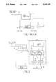
- FIG. 1 is a schematic diagram shown in block form illustrating a prior art analog phaselock loop (PLL);
- FIG. 2 is a schematic diagram shown in block form illustrating the preferred embodiment of a PLL in accordance with the present invention
- FIG. 3 shows a diagram of the Lock-in Range for a digital PLL, in which the Normalized Lock-in Range is plotted on the y-axis and the Least Significant Bit frequency change which affects the frequency of the VCO oscillator expressed in percentage points, is plotted on the x-axis;
- FIG. 4 shows a plot representing a Phase-plane analysis of a digital PLL that includes a digital Sequential Phase Error Detector (SPED); and
- FIG. 5 illustrates a detailed logic diagram of the Sequential Phase Error Detector as part of a PLL in accordance with the present invention.
- FIG. 1 there is shown a block diagram illustrating a prior art first order analog PLL indicated by reference number 1, that includes a free-running VCO 20.
- phase comparator 125 Conventional elements of a PLL are a phase comparator 125, a loop filter (not shown), and a frequency divider 30 as part of the feedback loop that includes the VCO 20.
- Phase comparator 10 generates a voltage level proportional to the phase difference of the VCO 20 output and the reference input clock 105 (not shown).
- the PLL implements a negative feedback control system which uses the phase comparator 125 output voltage to drive the VCO 20, such that the VCO output frequency is locked in its phase and frequency to the reference clock signal 105.
- a high-speed and low speed terminal are provided by tapping each side of the frequency divider circuit 30, and shown by lines 25 and 35, respectively.
- FIG. 2 shows a block diagram of a first order digital phaselock loop (PLL) according to the present invention.
- a flip-flop 125 digitally performs the analog operation of a phase comparator by holding a lead or lag signal on the falling transition. If the VCO 20 lags behind the frequency of the reference input signal, the counter 150 increments its count, which in turn increments the frequency of the VCO. Conversely, if the frequency of the VCO 20 leads that of the reference signal, the counter decrements its count, thereby reducing the frequency of the VCO.
- K the analog loop gain parameter, is determined by the frequency increment of the digitally controlled oscillator.
- the lock-in range and pull-in range for this digital implementation are the same and are illustrated in FIG. 3.
- FIG. 3 shows a plot of the upper and lower bounds of the frequencies over which a PLL can lock-in, for any normalized frequency between 90% and 115%.
- the x-axis is the Least Significant Bit (LSB) frequency step of the VCO expressed in percentage points, whereas the y-axis shows the normalized lock-in range.
- LSB Least Significant Bit
- First order PLL's suffer from a serious drawback which greatly limits their usefulness in many applications.
- the ability to adjust only one parameter, namely, the loop gain K causes a designer to trade-off jitter (i.e., noise) performance to accommodate a wider lock-in range and, hence, a wider pull-in range.
- jitter i.e., noise
- control of the VCO natural frequency must be extremely tight so that it will fall within the lock-in range of the PLL.
- a loop filter is incorporated in an analog PLL which integrates the output of the phase comparator or phase detector.
- the phase detector or phase comparator
- the output of the phase detector has a DC component which indicates the direction of the frequency error.
- the Sequential Phase Error Detector solves this limited pull-in range problem by extending the pull-range by ⁇ 50% of the frequency of the input reference signal.
- the input reference clock shall also be referred to henceforth as the free-running oscillator.
- phase-plane analysis is routinely used to illustrate graphically the operation of a non-linear system.
- State variables are chosen to represent a system parameter and its time derivative, which correspond in the present invention, to the frequency and phase error signals in the PLL.
- the system follows a trajectory in the phase-plane as time evolves that clearly elucidates the relationship between the state variables. It is evident to those skilled in the art, that many trajectories may exist in the phase-plane analysis, although the system only follows one that is based on its initial phase and frequency.
- the action of the PLL is to force the VCO 20 (FIG.
- phase- plane analysis has two distinct modes. The first occurs immediately after start-up and is characterized by large discontinuous phase swings which are indicative of cycle slips. The second has elliptical trajectories in the left and right halves, thereby indicating the absence of cycle slips, i.e., the phase error never reaches 180 degrees.
- the Sequential Phase Error Detector is active only while cycle slipping is occurring.
- the phase detector output is comprised of a sequence of lead phase samples followed by a sequence of lag samples.
- SPED detects the transition between lead and lag samples which indicates that a zero phase error condition has just passed.
- the detector examines the quadrature clock to determine if a cycle slip has occurred during the lead-lag transition. If it has (e.g., when a falling reference clock edge is aligned to a rising VCO edge) no corrective action is taken.
- the output of the phase detector indicates the direction which the coarse digital-to-analog DCC circuit 50 (FIG. 2) must be adjusted to.
- Lead/lag transitions are normally accompanied by alternating cycle slip events, as indicated by successive high and low levels on the quadrature clock, while the PLL is in a cycle slipping mode. If three successive lead/lag transitions are not associated with cycle slip events, then the VCO frequency remains within the lock-in range of the PLL.
- the SPED circuit freezes the frequency up-down counter (coarse adjustment) in its current state, thereby allowing the PLL to lock using the phase up-down counter (fine, adjustment). Detecting three non-cycle slip events, implies that the loop is locked-in and can subsequently be used as a lock indicator to an outside observer.
- FIG. 5 the Clock Generator or PLL is schematically shown.
- the PLL is a monolithic phaselock loop which is used to generate an internal two phase non-overlapping clock (+CLB0 and +CLB1, lines 122 and 124, respectively) which drives a bit serializer of a Transmitter Integrated Circuit chip, commonly used in an High Speed Optical Link, and well known to those proficient in the art.
- the function of the PLL is to phaselock the internal digitally controlled oscillator (or VCO) to a reference clock provided by the system (+REF 105).
- the serializer divides the frequency by 10 and feeds back the in-phase and quadrature clocks at a byte rate of 40 MHZ.
- the two internally phaselocked signals +RCLK 133 and +PCLK 110, henceforth referred to as ⁇ reference clock ⁇ and ⁇ in-phase clock ⁇ allow the Clock Generator to adjust the VCO frequency and thereby synchronize the falling edges of these two signals.
- +RCLK 133 samples the state of +PCLK 110 and stores this value at the latch 125 output +COMP.
- a latch shall be referred to interchangeably as flip-flop.
- It also generates a negative pulse at line 135 starting two superbuffer logic gate delays after a falling edge of +RCLK 133 and ending five gate delays later, thereby clocking the phase up-down counter 150. If +COMP is high, then counter 150 counts up; conversely, if it is low, the counter counts down.
- This portion of the circuit implements a simple first order phaselock loop which, is mathematically unconditionally stable.
- the VCO must be designed to have enough range to compensate for temperature and power supply variations. Process variations result in a wide range of nominal VCO output frequency which are compensated by using digital control logic, as shown in FIG. 5.
- the VCO is controlled by a phase DAC only with the +COMP signal assuming 0 or 1 values depending on the relative position of the falling edges of RCLK and PCLK in time. Since the phase counter 150 must increment or decrement on each RCLK falling edge, the VCO frequency will change by the Least Significant Bit (LSB) amount on each cycle. Since the probability that the VCO frequency will exactly equal the desired 400 MHZ at any DAC input value is zero, the VCO frequency will alternate between two values which bracket the desired 400 MHZ rate with a duty cycle proportional to the relative error of the two values.
- LSB Least Significant Bit
- the transition detector consisting of latch 127, and preferably, 6 inverters and 1 XNOR gate (block 129) generate a negative pulse at -TRANS 131.
- This pulse clocks the three bit shift register PLLSR (block 170) which stores the last 3 values of -QCLK 168. If the last three values of -QCLK 168 are low, then the PLL is considered to be locked, and the lock indicator +LOCK 72 is asserted.
- the clock input to the frequency up-down counter 160 is disabled which in turn locks out the coarse frequency tuning used in the Frequency Acquisition mode.
- Latch 126 sets shift-register 170 and is itself set by a delayed signal originating from the frequency divider 30.
- the -QCLK 168 signal is used to disable the clock input to the frequency counter 160 whenever a cycle slip occurs. Since a large frequency error between RCLK and PCLK 110 exists at that time, the walkoff between these two signals will result in relatively long strings of 1's and 0's generated by COMP. After cycle slip, a long string of 1's or 0's will occur at COMP until both falling edges align again, after which a long string of the opposite values 0's or 1's will take place. When the falling edge of PCLK 110 slips past the falling edge of RCLK (not a slip cycle), a pulse will be generated at -TRANS 131 and the frequency counter 160 will be clocked on alternate -TRANS 131 pulses. Frequency Acquisition will remain in effect until the PDAC 152 (Phase DAC) can maintain lock, at which time the lock indicator +LOCK 172 will disable the clock input to the frequency counter 160.
- PDAC 152 Phase DAC
- the off-chip reference clock +REF 105 is additionally used to sample the output +PCLK 110 of the frequency divider circuit 30 which is driven by VCO 20. Moreover, it samples the quadrature clock +QCLK 100, which is, likewise, also generated by the frequency divider circuit 30.
- Reference clock +REF is additionally fed to a latch (block 103) which outputs provide signals of the same frequency but of different phase. This is relevant because the input signal to block 127 needs to be out-of-phase with the signal at +REF 105.
- the first order PLL is implemented using latch FDIT 125 as phase comparator, with inputs +RCLK 133 and +PCLK 110, a phase up-down counter 150, a VCO 20 and a frequency divider circuit 30.
- Phase samples of +PCLK 110 are taken by the latch FDIT 125 and held at +COMP 123 which controls the direction which the phase up-down counter 150 counts.
- a transition detector is implemented with a single-shot circuit 137 connected to the up-down counter 150, which emits a pulse at each falling edge transition of the +RCLK clock.
- the phase up-down counter 150 drives the fine PDAC 152 controlling the VCO 20.
- the VCO outputs +CLB0 122 and +CLB1 124 drive the frequency divider circuit 30 which generates, respectively +PCLK 110 and +QCLK 100, out-of-phase to each other by 90 degrees and delayed with respect to each other by half a cycle (via delay block 40).
- the Sequential Phase Error Detector circuit is likewise implemented in its preferred embodiment by latch FDITH 127 which holds the previous phase sample +Q2.
- latch FDITH 126 with an input provided by the delayed signal generated by the frequency divider 30, stores the value of +QCLK to provide data to shift-register 170.
- a transition detector is implemented with a single-shot circuit 129 which emits a pulse -TRANS 131 when the phase samples change from lead to lag or from lag to lead. This pulse probes the frequency up-down counter 160 and the shift register PLLSR 170. Shift-register 170 stores the history of +QCLK (line 100) which detects whether the loop is still cycle slipping.
- Frequency counter 160 is active only when +LOCK 172 is low, and is clocked when +QCLK 100 is high, thereby indicating a non-cycle slip event.
- the output of frequency counter 160 is connected to the coarse FDAC 162 which drives VCO 20, thereby giving the PLL an expanded pull-in range.
- the present invention has particular application to the design of a PLL which can pull-in over a wider range of frequencies than present day first order PLL's.
- the SPED circuit is instrumental in allowing the PLL to compensate for deviations in the natural frequency of the VCO which occur due to process variations, while at the same time, providing a low-jitter environment which is essential for low error rates.
- the Sequential Phase Error Detector (SPED) circuit in accordance with the present invention, is particularly well suited for a VCO with wide variations of its natural frequency, without which the circuit yield would be severely impacted. More significantly, it permits extending the pull-in range to ⁇ 50% of the input reference clock frequency.
- the PLL described in the present invention requires no system intervention to acquire synchronization on power-up. Furthermore, it also resynchronizes automatically if a noise burst causes the VCO to wander. This self-starting feature is ensured by limiting the allowable VCO frequency range PCLK to between 0.5 to 1.5 times the reference clock RCLK frequency. The VCO frequency, though, must fall within this range to guarantee that the PLL will acquire lock. The operating frequency is limited only by the range of the VCO.
- the one-shot circuit (block 137) used to generate the pulse at 135 must produce a pulse long enough to update the phase up-down counter 150.
- the pulse at -TRANS 131 must be long enough to update the frequency up-down counter 160.
- the pulse width for both signals is set by the corresponding inverter chain (block 129). +COMP must be valid to ensure that (135) increments and decrements the counter 150 appropriately, and -RCLK to ascertain that no false transitions are detected.
- the clock input inside the phase up-down counter 150 should be changed to be identical to the frequency up-down counter 160, thereby allowing the inverter that generates 135 to be removed.
Landscapes
- Stabilization Of Oscillater, Synchronisation, Frequency Synthesizers (AREA)
Priority Applications (3)
| Application Number | Priority Date | Filing Date | Title |
|---|---|---|---|
| US07/784,849 US5168245A (en) | 1991-10-30 | 1991-10-30 | Monolithic digital phaselock loop circuit having an expanded pull-in range |
| JP4266051A JP2771928B2 (ja) | 1991-10-30 | 1992-10-05 | フェーズロック・ループ回路 |
| EP19920203320 EP0540119A3 (en) | 1991-10-30 | 1992-10-28 | Monolithic digital phaselock loop circuit |
Applications Claiming Priority (1)
| Application Number | Priority Date | Filing Date | Title |
|---|---|---|---|
| US07/784,849 US5168245A (en) | 1991-10-30 | 1991-10-30 | Monolithic digital phaselock loop circuit having an expanded pull-in range |
Publications (1)
| Publication Number | Publication Date |
|---|---|
| US5168245A true US5168245A (en) | 1992-12-01 |
Family
ID=25133717
Family Applications (1)
| Application Number | Title | Priority Date | Filing Date |
|---|---|---|---|
| US07/784,849 Expired - Fee Related US5168245A (en) | 1991-10-30 | 1991-10-30 | Monolithic digital phaselock loop circuit having an expanded pull-in range |
Country Status (3)
| Country | Link |
|---|---|
| US (1) | US5168245A (fr) |
| EP (1) | EP0540119A3 (fr) |
| JP (1) | JP2771928B2 (fr) |
Cited By (32)
| Publication number | Priority date | Publication date | Assignee | Title |
|---|---|---|---|---|
| US5302916A (en) * | 1992-12-21 | 1994-04-12 | At&T Bell Laboratories | Wide range digital frequency detector |
| EP0610990A2 (fr) * | 1993-02-05 | 1994-08-17 | Philips Patentverwaltung GmbH | Boucle à verrouillage de phase numérique |
| US5343169A (en) * | 1992-03-31 | 1994-08-30 | Sgs-Thomson Microelectronics S.A. | Frequency locked loop |
| EP0615360A2 (fr) * | 1993-03-12 | 1994-09-14 | Nec Corporation | Circuit de synchronisation d'horloge |
| US5394444A (en) * | 1993-07-12 | 1995-02-28 | Motorola, Inc. | Lock detect circuit for detecting a lock condition in a phase locked loop and method therefor |
| US5465075A (en) * | 1994-01-03 | 1995-11-07 | Texas Instruments Incorporated | Phase-locked loop circuit with minimum output jitter and maximum frequency stability |
| US5572157A (en) * | 1992-02-24 | 1996-11-05 | Hitachi, Ltd. | Digital phase-looked loop circuit |
| US5612980A (en) * | 1995-03-22 | 1997-03-18 | Alcatel Network Systems, Inc. | Method and apparatus for fast lock time |
| WO1997025773A1 (fr) * | 1996-01-13 | 1997-07-17 | Robert Bosch Gmbh | Procede et dispositif pour la modulation de frequence d'un signal haute frequence |
| US5764712A (en) * | 1996-04-18 | 1998-06-09 | International Business Machines Corporation | Phase locked loop circuit having automatic range setting logic |
| US5838180A (en) * | 1996-09-12 | 1998-11-17 | Lucent Technologies Inc. | Low-voltage frequency synthesizer |
| US5942949A (en) * | 1997-10-14 | 1999-08-24 | Lucent Technologies Inc. | Self-calibrating phase-lock loop with auto-trim operations for selecting an appropriate oscillator operating curve |
| US6016331A (en) * | 1997-08-05 | 2000-01-18 | Vlsi Technology, Inc. | Methods of synchronization, personal handy-phone system stations and phase lock loops |
| GB2344006A (en) * | 1998-11-23 | 2000-05-24 | Motorola Inc | Direct modulation phase lock loop and method therefor |
| US6181168B1 (en) | 1999-09-24 | 2001-01-30 | Motorola, Inc. | High speed phase detector and a method for detecting phase difference |
| US6208211B1 (en) | 1999-09-24 | 2001-03-27 | Motorola Inc. | Low jitter phase locked loop having a sigma delta modulator and a method thereof |
| US6310568B1 (en) | 1999-11-24 | 2001-10-30 | Mitsubishi Denki Kabushiki Kaisha | Digital-to-analog conversion circuit |
| US6570947B1 (en) | 1999-09-24 | 2003-05-27 | Motorola, Inc. | Phase lock loop having a robust bandwidth and a calibration method thereof |
| US20040012448A1 (en) * | 2002-05-03 | 2004-01-22 | Jorg Bonhaus | PLL circuit and method for eliminating self-jitter in a signal which is received by a control circuit |
| US6798297B1 (en) * | 2002-11-20 | 2004-09-28 | Cypress Semiconductor Corporation | Method and apparatus for converging a control loop |
| US6947514B1 (en) * | 1997-06-27 | 2005-09-20 | Renesas Technology Corporation | Phase-locked loop circuit, information processing apparatus, and information processing system |
| US20060215798A1 (en) * | 2004-05-28 | 2006-09-28 | Nelson Dale H | Digitally controlled oscillator having enhanced control resolution |
| US20070057827A1 (en) * | 2005-09-14 | 2007-03-15 | Morrill David P | Method and apparatus for generating a serial clock without a PLL |
| US20070200635A1 (en) * | 2006-02-17 | 2007-08-30 | David Meltzer | Methods and apparatus for compensating a variable oscillator for process, voltage, and temperature variations using a replica oscillator |
| US7382848B2 (en) * | 1994-03-31 | 2008-06-03 | Stmicroelectronics, Inc. | First order tuning circuit for a phase-locked loop |
| US8237510B2 (en) | 2010-08-18 | 2012-08-07 | International Business Machines Corporation | Implementing phase locked loop (PLL) with enhanced locking capability with a wide range dynamic reference clock |
| US20150236708A1 (en) * | 2013-07-25 | 2015-08-20 | Boe Technology Group Co., Ltd. | Frequency Signal Generating System and Display Device |
| US20160094278A1 (en) * | 2014-09-30 | 2016-03-31 | Texas Instruments Incorporated | Control of a tank circuit in a wireless power transmission system providing fsk communication |
| CN107690751A (zh) * | 2015-06-16 | 2018-02-13 | 瑞典爱立信有限公司 | 正交相位检测器电路、正交相位校正器、多天线无线电电路、无线电站和方法 |
| CN108923782A (zh) * | 2018-07-19 | 2018-11-30 | 深圳大学 | 一种全数字锁相环及其快速锁相方法 |
| US10778034B2 (en) | 2013-12-16 | 2020-09-15 | Texas Instruments Incorporated | Circuit and architecture for a demodulator for a wireless power transfer system and method therefor |
| US20220326755A1 (en) * | 2015-12-15 | 2022-10-13 | Intel Corporation | Processor core energy management |
Families Citing this family (2)
| Publication number | Priority date | Publication date | Assignee | Title |
|---|---|---|---|---|
| US6636978B1 (en) * | 1999-11-17 | 2003-10-21 | International Business Machines Corporation | Rescheduling data input and output commands for bus synchronization by using digital latency shift detection |
| US8386829B2 (en) * | 2009-06-17 | 2013-02-26 | Macronix International Co., Ltd. | Automatic internal trimming calibration method to compensate process variation |
Citations (11)
| Publication number | Priority date | Publication date | Assignee | Title |
|---|---|---|---|---|
| US4131861A (en) * | 1977-12-30 | 1978-12-26 | International Business Machines Corporation | Variable frequency oscillator system including two matched oscillators controlled by a phase locked loop |
| US4456890A (en) * | 1982-04-05 | 1984-06-26 | Computer Peripherals Inc. | Data tracking clock recovery system using digitally controlled oscillator |
| US4531102A (en) * | 1983-02-28 | 1985-07-23 | Gk Technologies, Incorporated | Digital phase lock loop system |
| US4565976A (en) * | 1983-08-05 | 1986-01-21 | Advanced Micro Devices, Inc. | Interruptable voltage-controlled oscillator and phase-locked loop using same |
| US4570130A (en) * | 1982-10-20 | 1986-02-11 | International Business Machines Corporation | Input controller circuit apparatus for phase lock loop voltage controlled oscillator |
| US4799028A (en) * | 1986-07-02 | 1989-01-17 | Hughes Aircraft Company | Zero phase shift active microwave oscillators with resistive feedback in field effect transistor amplifiers |
| US4879530A (en) * | 1987-11-19 | 1989-11-07 | Siemens Aktiengesellschaft | Monolithically integratable phase shifter VCO |
| US4908582A (en) * | 1988-03-31 | 1990-03-13 | Kabushiki Kaisha Toshiba | AFC circuit for producing a ripple-free oscillator control voltage |
| US4920322A (en) * | 1988-02-25 | 1990-04-24 | At&T Philips Telecommunications | Voltage controlled r-c oscillator and phase locked loop |
| US4929916A (en) * | 1988-03-10 | 1990-05-29 | Nec Corporation | Circuit for detecting a lock of a phase locked loop |
| US4942370A (en) * | 1988-04-08 | 1990-07-17 | Ricoh Company, Ltd. | PLL circuit with band width varying in accordance with the frequency of an input signal |
Family Cites Families (14)
| Publication number | Priority date | Publication date | Assignee | Title |
|---|---|---|---|---|
| JPS5075351A (fr) * | 1973-11-05 | 1975-06-20 | ||
| JPS57183132A (en) * | 1981-05-06 | 1982-11-11 | Mitsubishi Electric Corp | Phase synchromizing circuit |
| US4516250A (en) * | 1983-08-26 | 1985-05-07 | At&T Information Systems | Frequency and phase comparator with slip detection capability |
| FR2600848B1 (fr) * | 1984-09-10 | 1992-06-05 | Labo Cent Telecommunicat | Dispositif d'asservissement d'un oscillateur a une source hyperfrequence a tres faible bruit de phase et agile en frequence |
| JPS62160821A (ja) * | 1986-01-10 | 1987-07-16 | Hitachi Ltd | バ−スト信号用pll回路 |
| JPS6331221A (ja) * | 1986-07-24 | 1988-02-09 | Nec Corp | 位相同期回路 |
| JPS63152217A (ja) * | 1986-12-17 | 1988-06-24 | Hitachi Ltd | 位相比較回路 |
| JP2518860B2 (ja) * | 1987-08-31 | 1996-07-31 | 富士通株式会社 | 位相同期回路 |
| US4764737A (en) * | 1987-11-20 | 1988-08-16 | Motorola, Inc. | Frequency synthesizer having digital phase detector with optimal steering and level-type lock indication |
| JPH01154625A (ja) * | 1987-12-10 | 1989-06-16 | Nec Corp | Pll同期検出回路 |
| JPH01243622A (ja) * | 1988-03-25 | 1989-09-28 | Hitachi Ltd | 位相同期ループ回路 |
| JPH02180429A (ja) * | 1988-12-29 | 1990-07-13 | Nec Corp | Pll回路 |
| US4929918A (en) * | 1989-06-07 | 1990-05-29 | International Business Machines Corporation | Setting and dynamically adjusting VCO free-running frequency at system level |
| US4975650A (en) * | 1989-07-24 | 1990-12-04 | Motorola, Inc. | Phase detector |
-
1991
- 1991-10-30 US US07/784,849 patent/US5168245A/en not_active Expired - Fee Related
-
1992
- 1992-10-05 JP JP4266051A patent/JP2771928B2/ja not_active Expired - Lifetime
- 1992-10-28 EP EP19920203320 patent/EP0540119A3/en not_active Ceased
Patent Citations (11)
| Publication number | Priority date | Publication date | Assignee | Title |
|---|---|---|---|---|
| US4131861A (en) * | 1977-12-30 | 1978-12-26 | International Business Machines Corporation | Variable frequency oscillator system including two matched oscillators controlled by a phase locked loop |
| US4456890A (en) * | 1982-04-05 | 1984-06-26 | Computer Peripherals Inc. | Data tracking clock recovery system using digitally controlled oscillator |
| US4570130A (en) * | 1982-10-20 | 1986-02-11 | International Business Machines Corporation | Input controller circuit apparatus for phase lock loop voltage controlled oscillator |
| US4531102A (en) * | 1983-02-28 | 1985-07-23 | Gk Technologies, Incorporated | Digital phase lock loop system |
| US4565976A (en) * | 1983-08-05 | 1986-01-21 | Advanced Micro Devices, Inc. | Interruptable voltage-controlled oscillator and phase-locked loop using same |
| US4799028A (en) * | 1986-07-02 | 1989-01-17 | Hughes Aircraft Company | Zero phase shift active microwave oscillators with resistive feedback in field effect transistor amplifiers |
| US4879530A (en) * | 1987-11-19 | 1989-11-07 | Siemens Aktiengesellschaft | Monolithically integratable phase shifter VCO |
| US4920322A (en) * | 1988-02-25 | 1990-04-24 | At&T Philips Telecommunications | Voltage controlled r-c oscillator and phase locked loop |
| US4929916A (en) * | 1988-03-10 | 1990-05-29 | Nec Corporation | Circuit for detecting a lock of a phase locked loop |
| US4908582A (en) * | 1988-03-31 | 1990-03-13 | Kabushiki Kaisha Toshiba | AFC circuit for producing a ripple-free oscillator control voltage |
| US4942370A (en) * | 1988-04-08 | 1990-07-17 | Ricoh Company, Ltd. | PLL circuit with band width varying in accordance with the frequency of an input signal |
Cited By (50)
| Publication number | Priority date | Publication date | Assignee | Title |
|---|---|---|---|---|
| US5841303A (en) * | 1992-02-24 | 1998-11-24 | Hitachi, Ltd. | Digital phase-locked loop circuit |
| US5572157A (en) * | 1992-02-24 | 1996-11-05 | Hitachi, Ltd. | Digital phase-looked loop circuit |
| US5343169A (en) * | 1992-03-31 | 1994-08-30 | Sgs-Thomson Microelectronics S.A. | Frequency locked loop |
| US5302916A (en) * | 1992-12-21 | 1994-04-12 | At&T Bell Laboratories | Wide range digital frequency detector |
| EP0610990A2 (fr) * | 1993-02-05 | 1994-08-17 | Philips Patentverwaltung GmbH | Boucle à verrouillage de phase numérique |
| EP0610990A3 (en) * | 1993-02-05 | 1995-09-13 | Philips Patentverwaltung | Digital phase-locked loop. |
| EP0615360A3 (fr) * | 1993-03-12 | 1997-07-16 | Nec Corp | Circuit de synchronisation d'horloge. |
| EP0615360A2 (fr) * | 1993-03-12 | 1994-09-14 | Nec Corporation | Circuit de synchronisation d'horloge |
| US5475325A (en) * | 1993-03-12 | 1995-12-12 | Nec Corporation | Clock synchronizing circuit |
| US5394444A (en) * | 1993-07-12 | 1995-02-28 | Motorola, Inc. | Lock detect circuit for detecting a lock condition in a phase locked loop and method therefor |
| US5465075A (en) * | 1994-01-03 | 1995-11-07 | Texas Instruments Incorporated | Phase-locked loop circuit with minimum output jitter and maximum frequency stability |
| US7382848B2 (en) * | 1994-03-31 | 2008-06-03 | Stmicroelectronics, Inc. | First order tuning circuit for a phase-locked loop |
| US5612980A (en) * | 1995-03-22 | 1997-03-18 | Alcatel Network Systems, Inc. | Method and apparatus for fast lock time |
| WO1997025773A1 (fr) * | 1996-01-13 | 1997-07-17 | Robert Bosch Gmbh | Procede et dispositif pour la modulation de frequence d'un signal haute frequence |
| US5764712A (en) * | 1996-04-18 | 1998-06-09 | International Business Machines Corporation | Phase locked loop circuit having automatic range setting logic |
| US5838180A (en) * | 1996-09-12 | 1998-11-17 | Lucent Technologies Inc. | Low-voltage frequency synthesizer |
| US6947514B1 (en) * | 1997-06-27 | 2005-09-20 | Renesas Technology Corporation | Phase-locked loop circuit, information processing apparatus, and information processing system |
| US6016331A (en) * | 1997-08-05 | 2000-01-18 | Vlsi Technology, Inc. | Methods of synchronization, personal handy-phone system stations and phase lock loops |
| US6198784B1 (en) | 1997-08-05 | 2001-03-06 | Vlsi Technology, Inc. | Methods of synchronizing a personal handy-phone system station and phase lock loops |
| US5942949A (en) * | 1997-10-14 | 1999-08-24 | Lucent Technologies Inc. | Self-calibrating phase-lock loop with auto-trim operations for selecting an appropriate oscillator operating curve |
| US6114920A (en) * | 1997-10-14 | 2000-09-05 | Lucent Technologies Inc. | Self-calibrating voltage-controlled oscillator for asynchronous phase applications |
| GB2344006A (en) * | 1998-11-23 | 2000-05-24 | Motorola Inc | Direct modulation phase lock loop and method therefor |
| GB2344006B (en) * | 1998-11-23 | 2001-01-17 | Motorola Inc | Phase lock loop and method therefor |
| US6181168B1 (en) | 1999-09-24 | 2001-01-30 | Motorola, Inc. | High speed phase detector and a method for detecting phase difference |
| US6208211B1 (en) | 1999-09-24 | 2001-03-27 | Motorola Inc. | Low jitter phase locked loop having a sigma delta modulator and a method thereof |
| US6570947B1 (en) | 1999-09-24 | 2003-05-27 | Motorola, Inc. | Phase lock loop having a robust bandwidth and a calibration method thereof |
| US6310568B1 (en) | 1999-11-24 | 2001-10-30 | Mitsubishi Denki Kabushiki Kaisha | Digital-to-analog conversion circuit |
| US20040012448A1 (en) * | 2002-05-03 | 2004-01-22 | Jorg Bonhaus | PLL circuit and method for eliminating self-jitter in a signal which is received by a control circuit |
| US6836188B2 (en) * | 2002-05-03 | 2004-12-28 | Infineon Technologies Ag | PLL circuit and method for eliminating self-jitter in a signal which is received by a control circuit |
| US6798297B1 (en) * | 2002-11-20 | 2004-09-28 | Cypress Semiconductor Corporation | Method and apparatus for converging a control loop |
| US20060215798A1 (en) * | 2004-05-28 | 2006-09-28 | Nelson Dale H | Digitally controlled oscillator having enhanced control resolution |
| US7496170B2 (en) * | 2004-05-28 | 2009-02-24 | Agere Systems Inc. | Digitally controlled oscillator having enhanced control resolution |
| CN101263697B (zh) * | 2005-09-14 | 2011-09-07 | 快捷半导体有限公司 | 不使用pll产生串行时钟的方法和装置 |
| US7248122B2 (en) | 2005-09-14 | 2007-07-24 | Fairchild Semiconductor Corporation | Method and apparatus for generating a serial clock without a PLL |
| WO2007037864A1 (fr) * | 2005-09-14 | 2007-04-05 | Fairchild Semiconductor Corporation | Procede et appareil de generation d'une horloge serie sans pll |
| US20070057827A1 (en) * | 2005-09-14 | 2007-03-15 | Morrill David P | Method and apparatus for generating a serial clock without a PLL |
| KR101299387B1 (ko) * | 2005-09-14 | 2013-08-22 | 페어차일드 세미컨덕터 코포레이션 | Pll 없이 직렬 클록을 생성하는 방법 및 장치 |
| US7355482B2 (en) | 2006-02-17 | 2008-04-08 | Seiko Epson Corporation | Methods and apparatus for compensating a variable oscillator for process, voltage, and temperature variations using a replica oscillator |
| US20070200635A1 (en) * | 2006-02-17 | 2007-08-30 | David Meltzer | Methods and apparatus for compensating a variable oscillator for process, voltage, and temperature variations using a replica oscillator |
| US8237510B2 (en) | 2010-08-18 | 2012-08-07 | International Business Machines Corporation | Implementing phase locked loop (PLL) with enhanced locking capability with a wide range dynamic reference clock |
| US20150236708A1 (en) * | 2013-07-25 | 2015-08-20 | Boe Technology Group Co., Ltd. | Frequency Signal Generating System and Display Device |
| US9425810B2 (en) * | 2013-07-25 | 2016-08-23 | Boe Technology Group Co., Ltd. | Frequency signal generating system and display device |
| US10778034B2 (en) | 2013-12-16 | 2020-09-15 | Texas Instruments Incorporated | Circuit and architecture for a demodulator for a wireless power transfer system and method therefor |
| US20160094278A1 (en) * | 2014-09-30 | 2016-03-31 | Texas Instruments Incorporated | Control of a tank circuit in a wireless power transmission system providing fsk communication |
| US9838084B2 (en) * | 2014-09-30 | 2017-12-05 | Texas Instruments Incorporated | Control of a tank circuit in a wireless power transmission system providing FSK communication |
| CN107690751A (zh) * | 2015-06-16 | 2018-02-13 | 瑞典爱立信有限公司 | 正交相位检测器电路、正交相位校正器、多天线无线电电路、无线电站和方法 |
| CN107690751B (zh) * | 2015-06-16 | 2021-01-12 | 瑞典爱立信有限公司 | 正交相位检测器电路、正交相位校正器、多天线无线电电路、无线电站和方法 |
| US20220326755A1 (en) * | 2015-12-15 | 2022-10-13 | Intel Corporation | Processor core energy management |
| CN108923782A (zh) * | 2018-07-19 | 2018-11-30 | 深圳大学 | 一种全数字锁相环及其快速锁相方法 |
| CN108923782B (zh) * | 2018-07-19 | 2021-09-07 | 深圳大学 | 一种全数字锁相环及其快速锁相方法 |
Also Published As
| Publication number | Publication date |
|---|---|
| EP0540119A2 (fr) | 1993-05-05 |
| JP2771928B2 (ja) | 1998-07-02 |
| JPH07264062A (ja) | 1995-10-13 |
| EP0540119A3 (en) | 1993-12-08 |
Similar Documents
| Publication | Publication Date | Title |
|---|---|---|
| US5168245A (en) | Monolithic digital phaselock loop circuit having an expanded pull-in range | |
| US5838178A (en) | Phase-locked loop and resulting frequency multiplier | |
| US4855683A (en) | Digital phase locked loop with bounded jitter | |
| US6587534B2 (en) | Delay lock loop with clock phase shifter | |
| US6285225B1 (en) | Delay locked loop circuits and methods of operation thereof | |
| US7323940B2 (en) | Adaptive cycle-slipped detector for unlock detection in phase-locked loop applications | |
| US6667663B2 (en) | Phase locked loop circuit | |
| US5313503A (en) | Programmable high speed digital phase locked loop | |
| US5406592A (en) | First order FLL/PLL system with low phase error | |
| US6005425A (en) | PLL using pulse width detection for frequency and phase error correction | |
| US20070080728A1 (en) | Phase adjustment circuit | |
| US7676014B2 (en) | Digital lock detector for phase-locked loop | |
| US6915081B2 (en) | PLL circuit and optical communication reception apparatus | |
| US7142823B1 (en) | Low jitter digital frequency synthesizer and control thereof | |
| WO2004047300A1 (fr) | Circuit a boucle a verrouillage de phase a synchronisation de contour | |
| JPS63200618A (ja) | 位相同期ループ回路 | |
| EP2283575B1 (fr) | Système et procédé améliorés de prévention de glissement de cycle dans un synthétiseur de fréquence | |
| US5956379A (en) | Digital phase lock detector and low-pass filter selector | |
| US8866556B2 (en) | Phase shift phase locked loop | |
| US5420543A (en) | Method and apparatus for determining a constant gain of a variable oscillator | |
| WO2007084876A2 (fr) | Systèmes et procédés de réduction d'erreur de phase statique | |
| EP0703672A2 (fr) | Oscillateur contrÔlé numériquement | |
| US5126693A (en) | Circuit and method of reducing phase jitter in a phase lock loop | |
| US5546434A (en) | Dual edge adjusting digital phase-locked loop having one-half reference clock jitter | |
| US6249188B1 (en) | Error-suppressing phase comparator |
Legal Events
| Date | Code | Title | Description |
|---|---|---|---|
| AS | Assignment |
Owner name: INTERNATIONAL BUSINESS MACHINES CORPORATION, NEW Y Free format text: ASSIGNMENT OF ASSIGNORS INTEREST.;ASSIGNOR:KOSKOWICH, GREGORY N.;REEL/FRAME:005998/0027 Effective date: 19911024 |
|
| FPAY | Fee payment |
Year of fee payment: 4 |
|
| REMI | Maintenance fee reminder mailed | ||
| LAPS | Lapse for failure to pay maintenance fees | ||
| FP | Lapsed due to failure to pay maintenance fee |
Effective date: 20001201 |
|
| STCH | Information on status: patent discontinuation |
Free format text: PATENT EXPIRED DUE TO NONPAYMENT OF MAINTENANCE FEES UNDER 37 CFR 1.362 |