US5029249A - Electron microscope - Google Patents
Electron microscope Download PDFInfo
- Publication number
- US5029249A US5029249A US07/381,191 US38119189A US5029249A US 5029249 A US5029249 A US 5029249A US 38119189 A US38119189 A US 38119189A US 5029249 A US5029249 A US 5029249A
- Authority
- US
- United States
- Prior art keywords
- electron
- casing
- chamber
- sample chamber
- evacuation
- Prior art date
- Legal status (The legal status is an assumption and is not a legal conclusion. Google has not performed a legal analysis and makes no representation as to the accuracy of the status listed.)
- Expired - Fee Related
Links
- 238000010894 electron beam technology Methods 0.000 claims description 36
- 125000006850 spacer group Chemical group 0.000 claims description 14
- 238000004891 communication Methods 0.000 claims description 2
- 238000005266 casting Methods 0.000 claims 1
- 238000011109 contamination Methods 0.000 description 5
- 238000010276 construction Methods 0.000 description 3
- 238000009792 diffusion process Methods 0.000 description 3
- XEEYBQQBJWHFJM-UHFFFAOYSA-N Iron Chemical compound [Fe] XEEYBQQBJWHFJM-UHFFFAOYSA-N 0.000 description 2
- 230000005540 biological transmission Effects 0.000 description 2
- 230000000694 effects Effects 0.000 description 2
- 239000000696 magnetic material Substances 0.000 description 2
- 229910000851 Alloy steel Inorganic materials 0.000 description 1
- 230000001010 compromised effect Effects 0.000 description 1
- 238000013016 damping Methods 0.000 description 1
- 238000013461 design Methods 0.000 description 1
- 238000001514 detection method Methods 0.000 description 1
- 238000011161 development Methods 0.000 description 1
- 229910052742 iron Inorganic materials 0.000 description 1
- 239000000463 material Substances 0.000 description 1
- 230000003287 optical effect Effects 0.000 description 1
- 229910000889 permalloy Inorganic materials 0.000 description 1
- 230000000630 rising effect Effects 0.000 description 1
- 238000007789 sealing Methods 0.000 description 1
- 238000010561 standard procedure Methods 0.000 description 1
- 239000010959 steel Substances 0.000 description 1
- 238000012546 transfer Methods 0.000 description 1
Images


Classifications
-
- H—ELECTRICITY
- H01—ELECTRIC ELEMENTS
- H01J—ELECTRIC DISCHARGE TUBES OR DISCHARGE LAMPS
- H01J37/00—Discharge tubes with provision for introducing objects or material to be exposed to the discharge, e.g. for the purpose of examination or processing thereof
- H01J37/02—Details
- H01J37/18—Vacuum locks ; Means for obtaining or maintaining the desired pressure within the vessel
-
- H—ELECTRICITY
- H01—ELECTRIC ELEMENTS
- H01J—ELECTRIC DISCHARGE TUBES OR DISCHARGE LAMPS
- H01J37/00—Discharge tubes with provision for introducing objects or material to be exposed to the discharge, e.g. for the purpose of examination or processing thereof
- H01J37/02—Details
- H01J37/16—Vessels; Containers
Definitions
- the present invention relates to an electron microscope e.g, a scanning electron microscope or a transmission electron microscope.
- An electron microscope normally comprises a specimen chamber in which the specimen to be analysed is located, and an electron column which generates a beam of electrons which are used to bombard the specimen.
- That electron column itself normally has two parts, an electron gun chamber containing an electron gun for generating the beam of electrons, and a casing containing an electron lens arrangement.
- That electron lens arrangement usually includes a plurality of condenser lenses arranged vertically inside the casing with the electron beam passing down a central axis of those condenser lenses. Alignment coils for aligning the electrons into a narrow beam are located between the condenser and the electron gun.
- scanning coils deflection coils
- an electron beam path is defined between the electron gun and the sample, passing through the lenses and coils.
- the sample chamber must also be evacuated.
- the standard method of evacuating the interior of the electron column is to connect that column to a vacuum pump via a plurality of ducts which extend from the vacuum pump through the walls of the electron column.
- Example of such an arrangement is shown in Japanese patent application laid-open number 49-131376, in which there are three ducts extending from the electron column and one from the sample chamber which are interconnected at a diffusion pump.
- Japanese patent application laid-open number 55-136446 there are again a plurality of ducts leading from the electron column.
- the presence of such ducts causes a number of problems.
- the first problem is that, if a good vacuum is to be achieved within the electron column, it is necessary that the ducts be relatively large, so that they have satisfactory conductance.
- the size of the ducts is inconvenient, and limits the positioning of additional devices which may be heeded around the electron column, such as an X-ray system.
- a further problem associated with the presence of the ducts to the vacuum pump is that their presence means that apertures must be made in any magnetic shielding around the electron column. Stray magnetic fields may cause magnetic disturbance, and if this is allowed to affect the electron beam, the accuracy of the operation of the microscope may be compromised. For example, a magnetic disturbance due to e.g. noise may cause a ripple on the image produced by the electron microscope, thereby blurring that image. Therefore, in order to limit magnetic disturbance. it is known to place a shielding cylinder around the electron column, but it is necessary that apertures be made in that shielding to permit the ducting to the vacuum pump to emerge. Bearing in mind that that ducting needs to be large in order to achieve a good vacuum, there is thus a conflict between the need for a good vacuum and the need for good magnetic shielding.
- the present invention therefore seeks to overcome, or at least ameliorate, these problems.
- the present invention proposes that the ducting to the electron column which has been used in the prior art be dispensed with, and that the evacuation path of the electron gun chamber and/or casing containing the electron lens assembly, be defined within the casing itself.
- the beam path may be thought of as a suitable route for that evacuation path, but in fact that beam path will normally include a plurality of restricted apertures whose purpose is to collimate the beam, and therefore those small apertures would restrict the conductance of any evacuation path running along the beam path.
- the casing containing the electron lens assembly may be made from a closed enclosure, together with the electron gun chamber and the sample chamber. Then, by connecting suitable evacuation means in the form of e.g., a vacuum pump to the sample chamber, the whole interior can be evacuated.
- suitable evacuation means in the form of e.g., a vacuum pump
- the magnetic shielding since the ducting outside the electron column is dispensed with, it becomes possible for the magnetic shielding to be unbroken, except possibly where the electron microscope has an adjustable aperture (which is normally positioned between the condenser lenses and the deflection coils) since the control for that adjustable aperture has to project through the magnetic shielding.
- the magnetic shielding may simply extend along the casing, and be sealed to the outside of the sample chamber, but preferably there is a further shielding part which encloses the electron gun chamber.
- the evacuation path is defined within the casing, its size needs to be sufficiently large to permit a high conductance.
- suitable apertures between the electron gun chamber and the casing, adjacent the condenser lenses, and between the casing and the sample chamber permit a sufficiently high conductance to be achieved. Indeed, it is possible with the present invention to achieve a higher conductance than was normally achieved in standard arrangements using external ducting.
- Japanese patent application laid-open number 59-209045 apparently shows an arrangement in which there is no external ducting.
- the device shown in that disclosure is an electron analysing apparatus which involves the detection of Auger electrons, and therefore must operate under extremely high vacuum, much higher than is normally used in electron microscopes such as scanning electron microscopes or transmission electron microscopes. Therefore, one skilled in the art reading Japanese patent application laid-open number 59-209045 will immediately appreciate that what is illustrated is wholly schematic, and that additional ducting would be necessary in order to achieve the desired level of vacuum. Indeed, this can be seen from the fact that the arrangement is illustrated with the condenser lenses apparently directly contacting the vacuum, which would result in contamination and would not operate satisfactorily.
- the electron lenses should be sealed from the vacuum.
- those electron lenses be mounted in sealed modules, and a plurality of such modules be positioned within the casing of the electron.
- a bore extends through the centre of those modules, to define the electron beam path, but by suitable design of the modules, the evacuation path may be between the outer wall of those modules and the inner wall of the casing.
- the modules may be spaced by suitable spacers. It is desirable that those spacers have apertures therein so that they may thus form part of the evacuation path.
- the main limit on conductance from the electron gun chamber to the specimen chamber is at the mounting of the electron gun chamber to the casing, and the mounting of the casing to the specimen chamber.
- a plurality of apertures are usually necessary, and, particularly between the electron gun chamber and the casing, this may be achieved by providing a tie member in the form of a plate with a plurality of apertures therein.
- FIG. 1 shows a schematic sectional view through a scanning electron microscope being an embodiment of the present invention
- FIG. 2 shows, in sectional view, the structure of the electron column used in the electron microscope of FIG. 1;
- FIG. 3 shows a sectional view along the line A--A in FIG. 1;
- FIG. 4 shows a sectional view along the line B--B in FIG. 1;
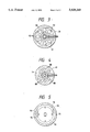
- FIG. 5 shows a view in the direction of the arrow P in FIG. 2.
- a scanning electron microscope comprises an electron column 10 (which will be described in more detail later) mounted on a specimen chamber 12. That specimen chamber is hollow, and a specimen support 14 extends into that hollow specimen chamber 12 for supporting a specimen 16 below the electron column.
- FIG. 1 also shows an enclosure 18 for magnetic shielding, from which extends a power cable 20 for powering the electron gun of the electron column.
- the specimen chamber is mounted on a stage 22 which is supported via damping supports 24 on a frame 26.
- FIG. 1 also illustrates the vacuum system for evacuating the specimen chamber 12.
- the duct 28 extends from that specimen chamber 12 and a first branch 30 extends via a valve 32 to a diffusion pump 40 which is itself connected via a valve 42 to the rotary pump 34.
- valves 38 and 42 are first closed, and the rotary pump operated to reduce the pressure within the specimen chamber 12.
- the valve 32 is closed and the valves 38 and 42 are opened.
- the diffusion pump 40 continues the evacuation of the specimen chamber 12 until a suitable vacuum has been achieved.
- vacuum systems may be used, however, such as e.g., a turbo-molecular pump.
- FIG. 2 shows the structure of the electron column in more detail, it can be seen that that column comprises a plurality of parts.
- the electron gun chamber containing an electron gun 44 which generates a beam of electrons.
- the electron gun chamber comprises an upper part 46 and a lower part 48 sealed together, the lower part being connected to a casing 50 for electron lenses via a spacer plate 52.
- the alignment coil assembly 54 which, as can be seen. has a bore 57 therein which forms part of the path of the electron beam. Although not illustrated, that bore 57 will normally contain a lining having only a small aperture therein to collimate the beam. It should be noted, that in order to prevent contamination, the alignment coil assembly 54 is hermetically sealed from the interior of the electron gun chamber 42 and the interior of the casing 50.
- the casing 50 contains a plurality of modules 56, 58 containing condenser electron lenses.
- FIG. 2 shows two such modules 56, 58, but more may be provided if necessary.
- Module 56 is shown in sectional view, and it can be seen there that the coils 60 of the lens are encased within magnetic shielding material formed by two shielding parts 62, 64.
- Power cables 66 extend from each module out of the casing 50 and are connected to a suitable power supply.
- Bores 68 extend down the centre of the modules to form the electron beam path, and these bores 68 may contain collimating apertures.
- each module 56, 58 is not sealed to the walls of the casing 50, but may simply be fitted therein provided that a close tolerance is achieved. It can be seen in FIG. 2 that each module has a flange 70 thereon which fits against the wall of the casing, with the rest of the module 56, 58 being of smaller diameter than the interior of the casing 50.
- the modules 56, 58 themselves are separated by a spacer 72, having openings 74 therein, and a further spacer 76 may be provided again having holes therein, between the upper module 58, and the spacer plate 52.
- the casing 50 is connected via a tie block 78 to the specimen chamber 12.
- a spacer 80 of non-magnetic material may be provided between that tie block 78 and the specimen chamber 12, with rings 82, 84 sealing the tie block 78 to the spacer 80 and the casing 50 respectively.
- a deflection coil unit 86 again having a bore therein to define the electron beam path, and attached to the bottom of the tie block 78 is an objective lens assembly 87.
- the resulting assembly is enclosed within the enclosure 18 for magnetic shielding, which enclosure comprises a lower shielding member 88 and an upper shielding member 90.
- the lower shielding member 88 is sealed to the outside of the specimen chamber 12, and extends to cover the tie block 78, the casing 50, and the lower part 48 of the electron gun chamber. It is this region which is most susceptible to magnetic disturbance.
- the shielding member 90 be provided covering the top of the electron gun chamber. As was mentioned earlier, it is important that this magnetic shielding be as continuous as possible to prevent magnetic disturbance of the electron beam, and it can be seen from FIG. 2 that the shielding is substantially continuous from the specimen chamber 12 to the electron gun chamber 43, and indeed may cover that chamber completely.
- control 93 of an adjustable aperture device which is located in the electron beam path. Since such a device is optional, the control 93 may be omitted in some cases, in which case the shielding may then be completely continuous.
- an evacuation path to permit evacuation of the interior of the electron column is provided within the casing 50 so that no ducting passes through the enclosure formed by the magnetic shield. This evacuation path will now be described in more detail.
- the tie block 78 has a plurality of bores 92 therein, thereby linking the interior of the casing 50 with the interior of the specimen chamber 12. Furthermore, the flange 70 of each lens module 56, 58, is cut, as can be seen for the lens module 56 in FIG. 5.
- FIG. 5 illustrates two cut-away parts 94, but in actuality, at least one cut-away is needed. That is, it is necessary to employ a construction which makes it possible to allow the condenser lens modules 56, 58 to fit the inside of the casing 50 and to keep an evacuation space therebetween.
- cut-away parts 94 and the spacings 96, 98 between the walls of the electron lens modules 56, 58 and the internal wall of the casing 50 permit a flow path around those modules 56, 58.
- the spacer plate 52 and the adjacent part of the lower part 48 of the electron gun chamber are provided with through-bores 99 as shown in FIG. 4.
- the evacuation path is defined from the sample chamber 12 to the interior of the electron gun chamber 42 through bores 92, cut-away parts 94, spacings 96, 98 and through-bores 99.
- K denotes the conductance coefficient given when a round pipeline is used
- d denotes inner diameter
- L denotes length
- the total value for seven bores is 58.8l/S.
- the conductance C 4 per through-bore is 12.4l/S obtained by the same operation as above.
- the conductance C 5 at the cut-away part is as follows:
- K denotes a conductance coefficient.
- K R denotes a square factor
- a and b respectively denote the long side and the short side of the rectangle
- the conductance C of the electron gun chamber can be computed from the above equation (2), but since the conductance given by the two cut-away parts 94 is far larger than that given by the bores 92 and through-bores 99 conductance C of the electron gun chamber may be neglected when computing the conductance of this embodiment as follows: ##EQU5##
- this embodiment can offer three times as much conductance as the prior art. It therefore serves to keep the electron gun chamber and the electron beam path in a high vacuum state as well as to suppress contamination in the overall system.
- this embodiment needs no opening for a pipeline in the enclosure 18 if the electron microscope is covered by the enclosure 18 for improving the magnetic shielding.
- more magnetic shielding and easier mounting and dismounting of the shielding cylinder may be achieved than in the prior art.
- the foregoing construction makes it possible to transfer the heat generated by the coil when the condenser lenses are excited to the casing as well as to prevent the temperature of the condenser lenses from rising. It is found that the flange 70 provides sufficient heat conduction despite the openings 94. Additional openings or holes could be used, but this could limit the heat conduction. Though the embodiment shown in FIG. 1 employs two condenser lens modules 56 and 58, at least one condenser lens is necessary.
- a magnetic material such as pure iron, soft steel, or Permalloy for the tie block and the casing.
- the coils are hermetically isolated from the vacuum and a high conductance is achieved for communication between the specimen chamber 12, the interior of the casing, the electron beam path, and the electron gun chamber. It is therefore possible to suppress contamination in the path where the electron beam passes and to keep the space at high vacuum.
Applications Claiming Priority (2)
| Application Number | Priority Date | Filing Date | Title |
|---|---|---|---|
| JP63-182991 | 1988-07-22 | ||
| JP63182991A JPH0760661B2 (ja) | 1988-07-22 | 1988-07-22 | 電子顕微鏡 |
Publications (1)
| Publication Number | Publication Date |
|---|---|
| US5029249A true US5029249A (en) | 1991-07-02 |
Family
ID=16127843
Family Applications (1)
| Application Number | Title | Priority Date | Filing Date |
|---|---|---|---|
| US07/381,191 Expired - Fee Related US5029249A (en) | 1988-07-22 | 1989-07-18 | Electron microscope |
Country Status (4)
| Country | Link |
|---|---|
| US (1) | US5029249A (de) |
| EP (1) | EP0352085B1 (de) |
| JP (1) | JPH0760661B2 (de) |
| DE (1) | DE68919004T2 (de) |
Cited By (8)
| Publication number | Priority date | Publication date | Assignee | Title |
|---|---|---|---|---|
| US5200616A (en) * | 1990-12-20 | 1993-04-06 | Shimadzu Corporation | Environment controllable scanning probe microscope |
| US5748866A (en) * | 1994-06-30 | 1998-05-05 | International Business Machines Corporation | Virtual display adapters using a digital signal processing to reformat different virtual displays into a common format and display |
| US6297512B1 (en) * | 1998-03-31 | 2001-10-02 | Cirrus Logic, Inc. | Double shield for electron and ion beam columns |
| US6320194B1 (en) * | 1997-09-27 | 2001-11-20 | Institute Of Materials Research And Engineering | Portable high resolution scanning electron microscope column using permanent magnet electron lenses |
| US6452173B1 (en) * | 1998-05-21 | 2002-09-17 | Seiko Instruments Inc. | Charged particle apparatus |
| US20020148971A1 (en) * | 2001-03-05 | 2002-10-17 | Michael Sogard | Lens assembly for electron beam column |
| US6515282B1 (en) * | 2000-03-28 | 2003-02-04 | Applied Materials, Inc. | Testing of interconnection circuitry using two modulated charged particle beams |
| US20070057185A1 (en) * | 2005-09-14 | 2007-03-15 | Hitachi High-Technologies Corporation | Electron beam device and its control method |
Families Citing this family (2)
| Publication number | Priority date | Publication date | Assignee | Title |
|---|---|---|---|---|
| DE602007007468D1 (de) | 2007-07-27 | 2010-08-12 | Integrated Circuit Testing | Magnetische Linsenanordnung |
| CN102163529B (zh) * | 2011-03-15 | 2012-07-25 | 北京航空航天大学 | 电子显微镜的聚光镜用可动光阑装置 |
Citations (11)
| Publication number | Priority date | Publication date | Assignee | Title |
|---|---|---|---|---|
| US3346736A (en) * | 1964-09-22 | 1967-10-10 | Applied Res Lab Inc | Electron probe apparatus having an objective lens with an aperture for restricting fluid flow |
| US3535515A (en) * | 1967-06-14 | 1970-10-20 | Us Navy | Ultrasonic apparatus for electron microscope |
| US3560739A (en) * | 1968-03-26 | 1971-02-02 | Otto Wolff | Particle beam apparatus for selectively forming an image of a specimen or its diffraction diagram |
| US3916201A (en) * | 1973-02-16 | 1975-10-28 | Siemens Ag | Electron microscope having a plurality of coaxial cryogenically cooled lenses |
| US4691103A (en) * | 1984-07-25 | 1987-09-01 | U.S. Philips Corporation | Microscope for non-differentiated phase image formation |
| US4694171A (en) * | 1984-11-29 | 1987-09-15 | Fuji Photo Film Co., Ltd. | Electron microscope image focusing using instantaneous emission of stimulable phosphor sheet |
| US4803369A (en) * | 1986-01-10 | 1989-02-07 | Hitachi, Ltd. | Purification device for charged particle beam diaphragm |
| US4806766A (en) * | 1986-06-25 | 1989-02-21 | U.S. Philips Corporation | Magnetic lens system |
| US4812652A (en) * | 1984-06-22 | 1989-03-14 | Carl-Zeiss Stiftung | Imaging method and apparatus for electron microscopes |
| US4814615A (en) * | 1986-05-06 | 1989-03-21 | Hitachi, Ltd. | Method and apparatus for detecting defect in circuit pattern of a mask for X-ray exposure |
| US4823006A (en) * | 1987-05-21 | 1989-04-18 | Electroscan Corporation | Integrated electron optical/differential pumping/imaging signal detection system for an environmental scanning electron microscope |
Family Cites Families (5)
| Publication number | Priority date | Publication date | Assignee | Title |
|---|---|---|---|---|
| US2637000A (en) * | 1951-02-15 | 1953-04-28 | Magnetic electron -lens | |
| GB1213374A (en) * | 1968-10-15 | 1970-11-25 | Ass Elect Ind | Improvements in or relating to electron optical systems |
| JPS51110964A (ja) * | 1975-03-26 | 1976-09-30 | Hitachi Ltd | Sosagatadenshikenbikyo |
| JPS5398772A (en) * | 1977-02-09 | 1978-08-29 | Hitachi Ltd | Corpuscular ray unit having atomosphere containing argon |
| JPS6322062U (de) * | 1986-07-26 | 1988-02-13 |
-
1988
- 1988-07-22 JP JP63182991A patent/JPH0760661B2/ja not_active Expired - Lifetime
-
1989
- 1989-07-18 US US07/381,191 patent/US5029249A/en not_active Expired - Fee Related
- 1989-07-19 EP EP89307301A patent/EP0352085B1/de not_active Expired - Lifetime
- 1989-07-19 DE DE68919004T patent/DE68919004T2/de not_active Expired - Fee Related
Patent Citations (11)
| Publication number | Priority date | Publication date | Assignee | Title |
|---|---|---|---|---|
| US3346736A (en) * | 1964-09-22 | 1967-10-10 | Applied Res Lab Inc | Electron probe apparatus having an objective lens with an aperture for restricting fluid flow |
| US3535515A (en) * | 1967-06-14 | 1970-10-20 | Us Navy | Ultrasonic apparatus for electron microscope |
| US3560739A (en) * | 1968-03-26 | 1971-02-02 | Otto Wolff | Particle beam apparatus for selectively forming an image of a specimen or its diffraction diagram |
| US3916201A (en) * | 1973-02-16 | 1975-10-28 | Siemens Ag | Electron microscope having a plurality of coaxial cryogenically cooled lenses |
| US4812652A (en) * | 1984-06-22 | 1989-03-14 | Carl-Zeiss Stiftung | Imaging method and apparatus for electron microscopes |
| US4691103A (en) * | 1984-07-25 | 1987-09-01 | U.S. Philips Corporation | Microscope for non-differentiated phase image formation |
| US4694171A (en) * | 1984-11-29 | 1987-09-15 | Fuji Photo Film Co., Ltd. | Electron microscope image focusing using instantaneous emission of stimulable phosphor sheet |
| US4803369A (en) * | 1986-01-10 | 1989-02-07 | Hitachi, Ltd. | Purification device for charged particle beam diaphragm |
| US4814615A (en) * | 1986-05-06 | 1989-03-21 | Hitachi, Ltd. | Method and apparatus for detecting defect in circuit pattern of a mask for X-ray exposure |
| US4806766A (en) * | 1986-06-25 | 1989-02-21 | U.S. Philips Corporation | Magnetic lens system |
| US4823006A (en) * | 1987-05-21 | 1989-04-18 | Electroscan Corporation | Integrated electron optical/differential pumping/imaging signal detection system for an environmental scanning electron microscope |
Cited By (9)
| Publication number | Priority date | Publication date | Assignee | Title |
|---|---|---|---|---|
| US5200616A (en) * | 1990-12-20 | 1993-04-06 | Shimadzu Corporation | Environment controllable scanning probe microscope |
| US5748866A (en) * | 1994-06-30 | 1998-05-05 | International Business Machines Corporation | Virtual display adapters using a digital signal processing to reformat different virtual displays into a common format and display |
| US6320194B1 (en) * | 1997-09-27 | 2001-11-20 | Institute Of Materials Research And Engineering | Portable high resolution scanning electron microscope column using permanent magnet electron lenses |
| US6297512B1 (en) * | 1998-03-31 | 2001-10-02 | Cirrus Logic, Inc. | Double shield for electron and ion beam columns |
| US6452173B1 (en) * | 1998-05-21 | 2002-09-17 | Seiko Instruments Inc. | Charged particle apparatus |
| US6515282B1 (en) * | 2000-03-28 | 2003-02-04 | Applied Materials, Inc. | Testing of interconnection circuitry using two modulated charged particle beams |
| US20020148971A1 (en) * | 2001-03-05 | 2002-10-17 | Michael Sogard | Lens assembly for electron beam column |
| US20070057185A1 (en) * | 2005-09-14 | 2007-03-15 | Hitachi High-Technologies Corporation | Electron beam device and its control method |
| US7550724B2 (en) * | 2005-09-14 | 2009-06-23 | Hitachi High-Technologies Corporation | Electron beam device and its control method |
Also Published As
| Publication number | Publication date |
|---|---|
| EP0352085A3 (en) | 1990-11-28 |
| EP0352085B1 (de) | 1994-10-26 |
| DE68919004D1 (de) | 1994-12-01 |
| EP0352085A2 (de) | 1990-01-24 |
| JPH0233844A (ja) | 1990-02-05 |
| JPH0760661B2 (ja) | 1995-06-28 |
| DE68919004T2 (de) | 1995-03-16 |
Similar Documents
| Publication | Publication Date | Title |
|---|---|---|
| US5029249A (en) | Electron microscope | |
| US5563566A (en) | Cryogen-cooled open MRI superconductive magnet | |
| KR0172938B1 (ko) | 주위 전자 주사 현미경용 대물렌즈 조립체 | |
| US7544954B2 (en) | Device for operating gas in vacuum or low-pressure environment and for observation of the operation | |
| US5250808A (en) | Integrated electron optical/differential pumping/imaging signal system for an environmental scanning electron microscope | |
| US5177361A (en) | Electron energy filter | |
| US8933400B2 (en) | Inspection or observation apparatus and sample inspection or observation method | |
| US4833330A (en) | Anticontaminator for transmission electron microscopes | |
| CN1602431A (zh) | 开放式磁共振成像(mri)磁体系统 | |
| JP2002329471A (ja) | 電子ビーム鏡筒用レンズ部材 | |
| EP0770882A1 (de) | Offener supraleitender Magnet für die Bilderzeugung durch magnetische Resonanz mit Kühlung durch kryogenes Fluid | |
| US4458151A (en) | Electron microscope of a scanning type | |
| JPH1116525A (ja) | X線コンピュータトモグラフ装置 | |
| JP3139920B2 (ja) | エネルギフィルタおよびこれを備えた透過電子顕微鏡 | |
| US6833550B2 (en) | Electron microscope | |
| US20020153495A1 (en) | Magnetically shielded enclosures for housing charged-particle-beam systems | |
| JPS583585B2 (ja) | 電子顕徴鏡等の試料室 | |
| EP0250675A1 (de) | Supraleitender Magnet | |
| US4931744A (en) | Synchrotron radiation source and method of making the same | |
| US20240112878A1 (en) | Charged particle microscope having vacuum in specimen chamber | |
| WO2024002399A1 (en) | A multi-mode low-voltage electron microscope | |
| JPH10199458A (ja) | エネルギーフィルタ及びこれを備えた透過型電子顕微鏡 | |
| JP2002324997A (ja) | 磁気シールドルーム | |
| US3973125A (en) | Corpuscular-ray apparatus with a cryogenically cooled specimen space | |
| EP1722397A1 (de) | Vorrichtung zur Handhabung von Gas in Vakuum oder Niederdruck Umgebung von Elektronenstrahlmikroskopen und zur Überwachung des Betriebs |
Legal Events
| Date | Code | Title | Description |
|---|---|---|---|
| AS | Assignment |
Owner name: HITACHI, LTD., 6, KANDA SURUGADAI 4-CHOME, CHIYODA Free format text: ASSIGNMENT OF ASSIGNORS INTEREST.;ASSIGNOR:OHTAKA, TADASHI;REEL/FRAME:005525/0538 Effective date: 19890711 |
|
| FEPP | Fee payment procedure |
Free format text: PAYOR NUMBER ASSIGNED (ORIGINAL EVENT CODE: ASPN); ENTITY STATUS OF PATENT OWNER: LARGE ENTITY |
|
| FPAY | Fee payment |
Year of fee payment: 4 |
|
| REMI | Maintenance fee reminder mailed | ||
| AS | Assignment |
Owner name: FLINT INK CORPORATION, MICHIGAN Free format text: ASSIGNMENT OF ASSIGNORS INTEREST;ASSIGNOR:BASF CORPORATION;REEL/FRAME:007986/0794 Effective date: 19960430 |
|
| FPAY | Fee payment |
Year of fee payment: 8 |
|
| LAPS | Lapse for failure to pay maintenance fees | ||
| STCH | Information on status: patent discontinuation |
Free format text: PATENT EXPIRED DUE TO NONPAYMENT OF MAINTENANCE FEES UNDER 37 CFR 1.362 |
|
| FP | Lapsed due to failure to pay maintenance fee |
Effective date: 20030702 |