US4831597A - Dynamic random access semiconductor memory wherein the RAS and CAS strobes respectively select the bit line and word line pairs - Google Patents
Dynamic random access semiconductor memory wherein the RAS and CAS strobes respectively select the bit line and word line pairs Download PDFInfo
- Publication number
- US4831597A US4831597A US07/118,009 US11800987A US4831597A US 4831597 A US4831597 A US 4831597A US 11800987 A US11800987 A US 11800987A US 4831597 A US4831597 A US 4831597A
- Authority
- US
- United States
- Prior art keywords
- bit line
- voltage source
- address signal
- source
- line pair
- Prior art date
- Legal status (The legal status is an assumption and is not a legal conclusion. Google has not performed a legal analysis and makes no representation as to the accuracy of the status listed.)
- Expired - Lifetime
Links
Images


Classifications
-
- G—PHYSICS
- G11—INFORMATION STORAGE
- G11C—STATIC STORES
- G11C11/00—Digital stores characterised by the use of particular electric or magnetic storage elements; Storage elements therefor
- G11C11/21—Digital stores characterised by the use of particular electric or magnetic storage elements; Storage elements therefor using electric elements
- G11C11/34—Digital stores characterised by the use of particular electric or magnetic storage elements; Storage elements therefor using electric elements using semiconductor devices
- G11C11/40—Digital stores characterised by the use of particular electric or magnetic storage elements; Storage elements therefor using electric elements using semiconductor devices using transistors
- G11C11/401—Digital stores characterised by the use of particular electric or magnetic storage elements; Storage elements therefor using electric elements using semiconductor devices using transistors forming cells needing refreshing or charge regeneration, i.e. dynamic cells
- G11C11/4063—Auxiliary circuits, e.g. for addressing, decoding, driving, writing, sensing or timing
- G11C11/407—Auxiliary circuits, e.g. for addressing, decoding, driving, writing, sensing or timing for memory cells of the field-effect type
- G11C11/409—Read-write [R-W] circuits
- G11C11/4091—Sense or sense/refresh amplifiers, or associated sense circuitry, e.g. for coupled bit-line precharging, equalising or isolating
-
- G—PHYSICS
- G11—INFORMATION STORAGE
- G11C—STATIC STORES
- G11C11/00—Digital stores characterised by the use of particular electric or magnetic storage elements; Storage elements therefor
- G11C11/21—Digital stores characterised by the use of particular electric or magnetic storage elements; Storage elements therefor using electric elements
- G11C11/34—Digital stores characterised by the use of particular electric or magnetic storage elements; Storage elements therefor using electric elements using semiconductor devices
- G11C11/40—Digital stores characterised by the use of particular electric or magnetic storage elements; Storage elements therefor using electric elements using semiconductor devices using transistors
- G11C11/401—Digital stores characterised by the use of particular electric or magnetic storage elements; Storage elements therefor using electric elements using semiconductor devices using transistors forming cells needing refreshing or charge regeneration, i.e. dynamic cells
- G11C11/4063—Auxiliary circuits, e.g. for addressing, decoding, driving, writing, sensing or timing
- G11C11/407—Auxiliary circuits, e.g. for addressing, decoding, driving, writing, sensing or timing for memory cells of the field-effect type
- G11C11/409—Read-write [R-W] circuits
- G11C11/4096—Input/output [I/O] data management or control circuits, e.g. reading or writing circuits, I/O drivers or bit-line switches
Definitions
- This invention relates to a dynamic random access semiconductor memory device which can decrease access time.
- the integration density of a dynamic random access semiconductor memory device is more and more improved with an advance in the microminiaturization technique. That is, the performance of memory cells is improved through the microminiaturization of memory cells and a great improvement has been achieved in the access time of the memory cells. If the gate length of the MOS transistors in a memory is reduced on the order of 0.5 ⁇ m in odder to effect that microminiaturization, a voltage which is applied to the memory cell has to be lowered so as to secure the reliability of memory cells. The limit has already been reached for the dRAM to operate at high speed with the use of microminiaturized memory cells.
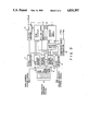
- memory cell array 1 is comprised of a matrix array of memory cells.
- Reference numeral 2 shows a multiplex address signal; 3, an address data buffer; 4, a column address buffer; 5, a row address buffer, 6 and 7 clock generators; 8, a column decoder; 9, a row decoder; 10, a bit line sense amplifier, 11, word lines; 12, bit lines; 13, an output data buffer; 14, a refresh counter; and 15, a substrate bias signal generator.
- Multiplex address signal 2 contains row and column address signals.
- the column address signal is responsive to a CAS (column address strobe) signal to allow it to be coupled to column decoder 8 through address data buffer 3 and column address buffer 4.
- the row address signal is responsive to a RAS (row address strobe signal) to allow it to be coupled to row decoder 9 through address data buffer 3 and row address buffer 5.
- the output of row decoder 9 selects word line 11 while, on the other hand, the output of column decoder 8 selects bi line 12.
- Bit line sense amplifier 10 is connected between a bit line pair and an I/O (input/output) line pair to amplify a memory cell output so that it is supplied to an I/O line.
- a row address is supplied to row address buffer 5 in response to the RAS signal, so that a word line is selected.
- a column address is supplied to column address buffer 4 in response to the CAS signal, so that a bit line is selected.
- bipolar transistors have not been used as driving transistors.
- the object of this invention is to provide a dynamic random access semiconductor memory device which can decrease access time with the use of different selection timings for bit and word lines and of a different arrangement of a bit line sense amplifier from the counterpart of a conventional dRAM.
- a dynamic random access semiconductor memory device which includes a plurality of dynamic random access memory cells integrated on a semiconductor substrate, a means for selecting a word line pair and a bit line pair, connected to at least one of the aforementioned memory cells, by a multiplex address signal containing row and column address signals, and a bit line sense amplifier including a differential amplifier connected between the bit line pair and a corresponding I/O (input/output line pair.
- Driving transistors in the differential amplifier are comprised of bipolar transistors.
- the bit line pair is selected at a first timing by a row address signal of the multiplex address signal and the word line pair is selected, at a second timing following the aforementioned first timing, by a column address signal of the multiplex address signal.
- FIG. 1 is a block diagram showing a conventional dRAM
- FIG. 2 is a block diagram showing a dynamic random access semiconductor memory device according to an embodiment of this invention.
- FIG. 3 is a circuit diagram showing part of the block diagram of FIG. 2, and
- FIG. 4 is an operation timing diagram of FIG. 3.
- a dynamic random access semiconductor memory device (dRAM) according to the embodiment of this invention will be explained below with reference to FIGS. 2 to 4.
- FIG. 2 the same reference numerals are employed to designate parts or elements corresponding to those shown in FIG. 1.
- the dRAM of this invention (FIG. 2) is different from the conventional dRAM in the following respects.
- a row address signal of a multiplex address signal is coupled to row address buffer 5 in response to a RAS signal and, in this case, a bit line pair, BL, BL is selected as opposed to the case where a word line pair WL, DWL is selected in the prior art.
- a column address signal is coupled to column address buffer 4 in response to a CAS signal, so that a word line pair WL, DWL is selected as opposed to the case where a bit line pair BL, BL is selected at said subsequent timing in the prior art.
- bipolar transistors are employed as driving transistors for a bit line sense amplifier connected to a bit line pair, noting that in the prior art MOS transistors have been used as the driving transistors.
- FIG. 3 is a circuit diagram showing an interconnecting relation among a memory cell, a bit line pair, a word line pair, a bit line sense amplifier and an I/O line pair in the dRAM of this invention.
- the bit line pair contains first and second bit lines BL and BL.
- the memory cell MC is comprised of one MOS transistor Q having its drain connected to the first bit line BL and one capacitor C S connected between the source of MOS transistor Q and source voltage source Vss.
- C B in FIG. 3 represents a capacitance for the bit line BL.
- the MOS transistor Q has its gate connected to a word line WL.
- a dummy memory cell DC is comprised of one dummy MOS transistor Q having its drain connected to the second bit line BL and one dummy capacitor CDS connected between the source of the MOS transistor Q and the source voltage source Vss.
- C B a capacitance on the bit line BL.
- the dummy MOS transistor Q has its gate connected to dummy word line DWL.
- Reference numeral 20 in FIG. 3 represents a CMOS F.F, (Complementary MOS flip-flop or data restore circuit) which serves to restore data corresponding to a memory cell.
- Output nodes 20 1 and 20 2 of the CMOS F.F. are connected to the bit lines BL and BL, respectively.
- Differential amplifier 22 constituting a bit line sense amplifier and connected between the drain voltage source Vcc and the source voltage source Vss includes first and second bipolar driving transistors T 13 and T 14 , bipolar load transistors T 11 and T 12 , P channel MOS transistors Q P4 , Q P5 , and n channel MOS transistor Q N8 connected between the emitters of transistors T 13 and T.sub.
- I/O and I/O lines are connected to output nodes 22 1 and 22 2 , respectively, and to a write gate circuit 25.
- Write gate circuit 25 includes a series circuit of MOS transistors Q N9 and Q N11 connected between the I/O line and the bit line BL with the gates of Q N9 and Q N11 supplied with a write control signal ⁇ W and column selection signal ⁇ 1 , respectively, and series circuit of MOS transistors Q N10 and Q N12 connected between the I/O line and the bit line BL with the gates of MOS transistors Q N10 and Q N12 supplied with a write control signal ⁇ W and column selection signal ⁇ 1 , respectively.
- First C 2 MOS inverter (clocked complementary MOS inverter) 23 is connected between the bit line BL and the base of first driving transistor T 13
- second C 2 MOS inverter 24 is connected between the bit line BL and the base of second driving transistor T 14 .
- These C 2 MOS inverters are used to provide a DC separation between the bit line BL and the output node 23 1 and between the bit line BL and output node 24 1 .
- First C z MOS inverter 23 includes a series circuit of P channel MOS transistors Q P6 and Q P7 connected between the drain voltage source Vcc and output node 23 1 with the gate of MOS transistor Q P7 connected to the bit line BL and with the gate of MOS transistor Q P6 supplies with the clock ⁇ 1 .
- First C 2 MOS inverter 23 further includes a series circuit of n channel MOS transistors Q N4 and Q N5 connected between the source voltage source Vss and output node 23 1 with the gate of transistor Q N4 connected to the bit line BL and with the gate of transistor Q N5 supplied with the clock ⁇ 1 .
- Second C 2 MOS inverter 24 includes a series circuit of MOS transistors Q P8 and Q P9 connected between the drain voltage source Vcc and output node 24 1 with the gate of transistor Q P9 connected to the bit line BL and with the gate of transistor Q P8 supplied with the clock ⁇ 1 .
- a series circuit of n channel MOS transistors Q N6 and Q N7 is connected between the source voltage source Vss and output node 24 1 with the gate of transistor Q N6 connected to the bit line BL and with the gate of transistor Q N7 supplied with the clock ⁇ 1 .
- a RAS (row address strobe) signal falls at a first timing and a row address signal is fed to row address buffer 5 which in turn supplies it to row decoder 9. Then, the clock ⁇ 1 rises and C 2 MOS inverters 23 and 24 are activated. Nearly at the same time the aforementioned clock ⁇ 2 rises and differential amplifier 22 is activated.
- a CAS (column address strobe) signal falls and a column address signal is supplied to column address buffer 4. The column address is decoded by column decoder 8 to produce a decoded column address signal by which the word line WL and dummy word line DWL are selected.
- the data of the memory cell MC is transferred to the bit line pair BL, BL and, at the same time, input to differential amplifier 22 where it is amplified.
- the amplified data is transferred to the I/O line pair I/O, I/O.
- output data buffer 13 are also comprised of a differential amplifier including bipolar driving transistors, data can be taken out of data output terminal Dout without requiring any clock control.
- Restoring data into a memory cell is achieved by sequentially supplying the clock ⁇ N to the gate of n channel MOS transistor Q N3 and the clock ⁇ p to the gate of p channel MOS transistor Q P3 to cause F.F. (data restore circuit) to be activated.
- F.F. data restore circuit
- a dRAM which can perform the same high-speed operation as a sRAM (static random access memory), while retaining the high degree of integration of the memory cells.
- the access time is of the order of 96 nsec
- the dRAM of this invention has been able to make the access time one half that of the conventional counterpart.
- the sensitivity of a bit line sense amplifier is determined by a ratio of the capacitance of the capacitor C S in the memory cell MC to the bit line capacitance C B . Therefore, it has been necessary in the prior art to make the capacitance C S at a value of over 40 fF so that the sensitivity of the bit line sense amplifier may not be lowered.
- the sense amplifier can adequately operate because the current amplifying type bit line sense amplifier is employed.
- a complicated cell manufacture step is involved in achieving a capacitor C S of over 40 fF, resulting in lower yield and in increased cost. According to this invention it is possible to make the manufacturing step simpler and lower in cost.
Landscapes
- Engineering & Computer Science (AREA)
- Microelectronics & Electronic Packaging (AREA)
- Computer Hardware Design (AREA)
- Databases & Information Systems (AREA)
- Dram (AREA)
Applications Claiming Priority (2)
| Application Number | Priority Date | Filing Date | Title |
|---|---|---|---|
| JP61-279931 | 1986-11-25 | ||
| JP61279931A JPS63133395A (ja) | 1986-11-25 | 1986-11-25 | 半導体記憶装置 |
Publications (1)
| Publication Number | Publication Date |
|---|---|
| US4831597A true US4831597A (en) | 1989-05-16 |
Family
ID=17617907
Family Applications (1)
| Application Number | Title | Priority Date | Filing Date |
|---|---|---|---|
| US07/118,009 Expired - Lifetime US4831597A (en) | 1986-11-25 | 1987-11-09 | Dynamic random access semiconductor memory wherein the RAS and CAS strobes respectively select the bit line and word line pairs |
Country Status (2)
| Country | Link |
|---|---|
| US (1) | US4831597A (ja) |
| JP (1) | JPS63133395A (ja) |
Cited By (16)
| Publication number | Priority date | Publication date | Assignee | Title |
|---|---|---|---|---|
| US4999815A (en) * | 1990-02-13 | 1991-03-12 | International Business Machines Corporation | Low power addressing systems |
| US5077693A (en) * | 1990-08-06 | 1991-12-31 | Motorola, Inc. | Dynamic random access memory |
| US5083296A (en) * | 1989-08-28 | 1992-01-21 | Hitachi, Ltd. | Semiconductor memory with alternately multiplexed row and column addressing |
| EP0468135A2 (en) * | 1990-06-29 | 1992-01-29 | International Business Machines Corporation | A high speed dynamic, random access memory with extended reset/precharge time |
| US5119336A (en) * | 1988-09-27 | 1992-06-02 | Nec Corporation | Memory write protection circuit |
| US5134616A (en) * | 1990-02-13 | 1992-07-28 | International Business Machines Corporation | Dynamic ram with on-chip ecc and optimized bit and word redundancy |
| US5301148A (en) * | 1989-08-04 | 1994-04-05 | Fujitsu Limited | Semiconductor memory device with bipolar-FET sense amp |
| US5347491A (en) * | 1991-04-11 | 1994-09-13 | Nec Corporation | Dynamic random access memory device having autorefreshing unit for producing internal row address strobe signal and internal column address strobe signal |
| US5553024A (en) * | 1989-06-21 | 1996-09-03 | Kabushiki Kaisha Toshiba | Semiconductor memory utilizing RAS and CAS signals to control the latching of first and second read or write data |
| USRE35680E (en) * | 1988-11-29 | 1997-12-02 | Matsushita Electric Industrial Co., Ltd. | Dynamic video RAM incorporating on chip vector/image mode line modification |
| USRE35921E (en) * | 1988-11-29 | 1998-10-13 | Matsushita Electric Industrial Co., Ltd. | Dynamic video RAM incorporating single clock random port control |
| US6209071B1 (en) | 1996-05-07 | 2001-03-27 | Rambus Inc. | Asynchronous request/synchronous data dynamic random access memory |
| US6639862B2 (en) * | 2001-03-23 | 2003-10-28 | Infineon Technologies Ag | Semiconductor memory with refresh and method for operating the semiconductor memory |
| USRE38379E1 (en) * | 1989-08-28 | 2004-01-06 | Hitachi, Ltd. | Semiconductor memory with alternately multiplexed row and column addressing |
| US8248884B2 (en) | 1997-10-10 | 2012-08-21 | Rambus Inc. | Method of controlling a memory device having multiple power modes |
| US9117499B2 (en) | 2012-10-25 | 2015-08-25 | Elwha Llc | Bipolar logic gates on MOS-based memory chips |
Citations (3)
| Publication number | Priority date | Publication date | Assignee | Title |
|---|---|---|---|---|
| JPS61142594A (ja) * | 1984-12-17 | 1986-06-30 | Hitachi Ltd | 半導体記憶装置 |
| US4656613A (en) * | 1984-08-29 | 1987-04-07 | Texas Instruments Incorporated | Semiconductor dynamic memory device with decoded active loads |
| US4685089A (en) * | 1984-08-29 | 1987-08-04 | Texas Instruments Incorporated | High speed, low-power nibble mode circuitry for dynamic memory |
-
1986
- 1986-11-25 JP JP61279931A patent/JPS63133395A/ja active Pending
-
1987
- 1987-11-09 US US07/118,009 patent/US4831597A/en not_active Expired - Lifetime
Patent Citations (3)
| Publication number | Priority date | Publication date | Assignee | Title |
|---|---|---|---|---|
| US4656613A (en) * | 1984-08-29 | 1987-04-07 | Texas Instruments Incorporated | Semiconductor dynamic memory device with decoded active loads |
| US4685089A (en) * | 1984-08-29 | 1987-08-04 | Texas Instruments Incorporated | High speed, low-power nibble mode circuitry for dynamic memory |
| JPS61142594A (ja) * | 1984-12-17 | 1986-06-30 | Hitachi Ltd | 半導体記憶装置 |
Cited By (27)
| Publication number | Priority date | Publication date | Assignee | Title |
|---|---|---|---|---|
| US5119336A (en) * | 1988-09-27 | 1992-06-02 | Nec Corporation | Memory write protection circuit |
| USRE35921E (en) * | 1988-11-29 | 1998-10-13 | Matsushita Electric Industrial Co., Ltd. | Dynamic video RAM incorporating single clock random port control |
| USRE35680E (en) * | 1988-11-29 | 1997-12-02 | Matsushita Electric Industrial Co., Ltd. | Dynamic video RAM incorporating on chip vector/image mode line modification |
| US5553024A (en) * | 1989-06-21 | 1996-09-03 | Kabushiki Kaisha Toshiba | Semiconductor memory utilizing RAS and CAS signals to control the latching of first and second read or write data |
| US5301148A (en) * | 1989-08-04 | 1994-04-05 | Fujitsu Limited | Semiconductor memory device with bipolar-FET sense amp |
| USRE38379E1 (en) * | 1989-08-28 | 2004-01-06 | Hitachi, Ltd. | Semiconductor memory with alternately multiplexed row and column addressing |
| US5083296A (en) * | 1989-08-28 | 1992-01-21 | Hitachi, Ltd. | Semiconductor memory with alternately multiplexed row and column addressing |
| US5134616A (en) * | 1990-02-13 | 1992-07-28 | International Business Machines Corporation | Dynamic ram with on-chip ecc and optimized bit and word redundancy |
| US4999815A (en) * | 1990-02-13 | 1991-03-12 | International Business Machines Corporation | Low power addressing systems |
| EP0468135A3 (en) * | 1990-06-29 | 1994-08-17 | Ibm | A high speed dynamic, random access memory with extended reset/precharge time |
| EP0468135A2 (en) * | 1990-06-29 | 1992-01-29 | International Business Machines Corporation | A high speed dynamic, random access memory with extended reset/precharge time |
| US5077693A (en) * | 1990-08-06 | 1991-12-31 | Motorola, Inc. | Dynamic random access memory |
| US5347491A (en) * | 1991-04-11 | 1994-09-13 | Nec Corporation | Dynamic random access memory device having autorefreshing unit for producing internal row address strobe signal and internal column address strobe signal |
| US6542976B2 (en) | 1996-05-07 | 2003-04-01 | Rambus Inc. | Memory device having an internal register |
| US7315929B2 (en) | 1996-05-07 | 2008-01-01 | Rambus Inc. | Memory device |
| US20030061460A1 (en) * | 1996-05-07 | 2003-03-27 | Barth Richard Maurice | Asynchronous request/synchronous data dynamic random access memory |
| US6405296B1 (en) | 1996-05-07 | 2002-06-11 | Rambus Inc. | Asynchronous request/synchronous data dynamic random access memory |
| US6532522B1 (en) | 1996-05-07 | 2003-03-11 | Rambus Inc. | Asynchronous request/synchronous data dynamic random access memory |
| US6209071B1 (en) | 1996-05-07 | 2001-03-27 | Rambus Inc. | Asynchronous request/synchronous data dynamic random access memory |
| US7085906B2 (en) | 1996-05-07 | 2006-08-01 | Rambus Inc. | Memory device |
| US20070201280A1 (en) * | 1996-05-07 | 2007-08-30 | Rambus Inc. | Memory device |
| US8305839B2 (en) | 1997-10-10 | 2012-11-06 | Rambus Inc. | Memory device having multiple power modes |
| US8248884B2 (en) | 1997-10-10 | 2012-08-21 | Rambus Inc. | Method of controlling a memory device having multiple power modes |
| US6639862B2 (en) * | 2001-03-23 | 2003-10-28 | Infineon Technologies Ag | Semiconductor memory with refresh and method for operating the semiconductor memory |
| US9117499B2 (en) | 2012-10-25 | 2015-08-25 | Elwha Llc | Bipolar logic gates on MOS-based memory chips |
| US9240230B2 (en) | 2012-10-25 | 2016-01-19 | Elwha Llc | Bipolar logic gates on MOS-based memory chips |
| US9583164B2 (en) | 2012-10-25 | 2017-02-28 | Elwha Llc | Bipolar logic gates on MOS-based memory chips |
Also Published As
| Publication number | Publication date |
|---|---|
| JPS63133395A (ja) | 1988-06-06 |
Similar Documents
| Publication | Publication Date | Title |
|---|---|---|
| US4954992A (en) | Random access memory having separate read out and write in bus lines for reduced access time and operating method therefor | |
| US4831597A (en) | Dynamic random access semiconductor memory wherein the RAS and CAS strobes respectively select the bit line and word line pairs | |
| EP0464426A1 (en) | Semiconductor memory having improved sensing arrangement | |
| JPH0546040B2 (ja) | ||
| US4791616A (en) | Semiconductor memory device | |
| JPH029081A (ja) | 半導体記憶装置 | |
| EP0258715A2 (en) | Static random access memory having bi-cmos construction | |
| EP0027169A1 (en) | Sense amplifier for integrated memory array | |
| US4722074A (en) | Semiconductor storage unit with I/O bus precharging and equalization | |
| US4982367A (en) | Dynamic random access memory with well-balanced read-out voltage on bit line pair and operating method therefor | |
| KR0121777B1 (ko) | 고속 동작용 감지 증폭기 | |
| JP2939027B2 (ja) | 半導体記憶装置 | |
| KR890003373B1 (ko) | 씨모오스 반도체 메모리 장치의 입출력 회로 | |
| US4734889A (en) | Semiconductor memory | |
| US4380055A (en) | Static RAM memory cell | |
| JP2744144B2 (ja) | 半導体記憶装置 | |
| KR910004733B1 (ko) | 데이타 버스 리셋트 회로를 지닌 반도체 기억장치 | |
| JPH07211081A (ja) | 半導体記憶装置 | |
| US5754488A (en) | Apparatus and method for controlling a bit line sense amplifier having offset compensation | |
| US4926381A (en) | Semiconductor memory circuit with sensing arrangement free from malfunction | |
| JP2937719B2 (ja) | 半導体記憶装置 | |
| US5189639A (en) | Semiconductor memory device having bit lines capable of partial operation | |
| US5023842A (en) | Semiconductor memory having improved sense amplifiers | |
| KR0165987B1 (ko) | 빠른 판독 동작 속도를 갖는 동적 랜덤 억세스 메모리 소자 | |
| US6741491B2 (en) | Integrated dynamic memory, and method for operating the integrated dynamic memory |
Legal Events
| Date | Code | Title | Description |
|---|---|---|---|
| AS | Assignment |
Owner name: KABUSHIKI KAISHA TOSHIBA, JAPAN Free format text: ASSIGNMENT OF ASSIGNORS INTEREST.;ASSIGNOR:FUSE, TSUNEAKI;REEL/FRAME:005046/0345 Effective date: 19871028 |
|
| STCF | Information on status: patent grant |
Free format text: PATENTED CASE |
|
| FEPP | Fee payment procedure |
Free format text: PAYOR NUMBER ASSIGNED (ORIGINAL EVENT CODE: ASPN); ENTITY STATUS OF PATENT OWNER: LARGE ENTITY |
|
| FPAY | Fee payment |
Year of fee payment: 4 |
|
| FPAY | Fee payment |
Year of fee payment: 8 |
|
| FPAY | Fee payment |
Year of fee payment: 12 |